
 Open Access Article
 This Open Access Article is licensed under a
 Creative Commons Attribution 3.0 Unported Licence
Solution phase treatments of Sb2Se3 heterojunction photocathodes for improved water splitting performance†
Pardis
Adams
 a,
Fabrizio
Creazzo
a,
Thomas
Moehl
a,
Rowena
Crockett
b,
Peng
Zeng
c,
Zbynek
Novotny
de,
Sandra
Luber
a,
Wooseok
Yang
*fg and
S. David
Tilley
*a
a,
Fabrizio
Creazzo
a,
Thomas
Moehl
a,
Rowena
Crockett
b,
Peng
Zeng
c,
Zbynek
Novotny
de,
Sandra
Luber
a,
Wooseok
Yang
*fg and
S. David
Tilley
*a
aDepartment of Chemistry, University of Zurich, Zurich, Switzerland. E-mail: david.tilley@chem.uzh.ch
bAdvanced Material and Surfaces, EMPA, Dubendorf, Switzerland
cScientific Centre for Optical and Electron Microscopy (ScopeM), ETH, Zurich, Switzerland
dSwiss Light Source, Paul Scherrer Institute, Villigen-PSI, Switzerland
eLaboratory for Joining Technologies and Corrosion, EMPA, Dübendorf, Switzerland
fSchool of Chemical Engineering, Sungkyunkwan University (SKKU), Suwon, South Korea. E-mail: wooseok.yang@skku.edu
gSKKU Institute of Energy Science and Technology (SIEST), Sungkyunkwan University, Suwon 16419, Republic of Korea
First published on 21st March 2023
Abstract
Antimony selenide (Sb2Se3) is an auspicious material for solar energy conversion that has seen rapid improvement over the past ten years, but the photovoltage deficit remains a challenge. Here, simple and low-temperature treatments of the p–n heterojunction interface of Sb2Se3/TiO2-based photocathodes for photoelectrochemical water splitting were explored to address this challenge. The FTO/Ti/Au/Sb2Se3 (substrate configuration) stack was treated with (NH4)2S as an etching solution, followed by CuCl2 treatment prior to deposition of the TiO2 by atomic layer deposition. The different treatments show different mechanisms of action compared to similar reported treatments of the back Au/Sb2Se3 interface in superstrate configuration solar cells. These treatments collectively increased the onset potential from 0.14 V to 0.28 V vs. reversible hydrogen electrode (RHE) and the photocurrent from 13 mA cm−2 to 18 mA cm−2 at 0 V vs. RHE as compared to the untreated Sb2Se3 films. From SEM and XPS studies, it is clear that the etching treatment induces a morphological change and removes the surface Sb2O3 layer, which eliminates the Fermi-level pinning that the oxide layer generates. CuCl2 further enhances the performance due to the passivation of the surface defects, as supported by density functional theory molecular dynamics (DFT-MD) calculations, improving charge separation at the interface. The simple and low-cost semiconductor synthesis method combined with these facile, low-temperature treatments further increases the practical potential of Sb2Se3 for large-scale water splitting.
1. Introduction
Meeting the increasing energy demand of today's world whilst attempting to achieve net zero emissions is one of the top priorities of this century. The sun's ample energy availability makes it a potential candidate to meet such demand in a green and sustainable manner.1 Since solar-related energy sources are subject to weather fluctuations and the diurnal cycles, a practical solution is to store the energy in molecular bonds, as nature does through photosynthesis, such as those of H2, which can then be used as a fuel source. Therefore, the semiconductor-based conversion of solar energy to H2 by water splitting is advantageous for our already fuel-based economy to directly convert and store the energy within the same system.2–5 The constraints on photoelectrochemical (PEC) water-splitting cells arise from three fundamental system requirements: efficient photogenerated charge collection, harvesting a substantial fraction of the available solar energy, and long-term stability. Due to the inherent area-dependency and hence the amount of material used, the predominant way to make PEC cells more competitive is by increasing their solar to hydrogen (STH) efficiency.6 Sb2Se3 has recently gained popularity due to its potential to have similar STH efficiencies to crystalline silicon, the benchmark material for solar conversion technology. Sb2Se3 is a relatively cost-effective (Sb has a similar cost to Cu and Se has a similar cost to Sn) and reasonably abundant light-absorbing material, not listed as a “highly toxic” compound in many official records, as opposed to many other current semiconductor materials containing Cd and Pb.7 The melting point of Sb2Se3 lies at 608 °C, making it suitable for low-temperature processing and easy deposition. The Sb2Se3 polycrystalline films have no other stable binary phase and a quasi-one-dimensional (Q1D) crystal structure oriented along the [001] direction.8 As opposed to other widely explored 3D photovoltaic absorbers such as CIGS and GaAs, the Q1D Sb2Se3 has intrinsically benign grain boundaries (GB) along the ribbons and indeed at any crystallographic orientation due to the “self-healing” effect,9,10 hence avoiding major surface recombination losses that limit high-efficiency thin-films. As a light absorber material for solar cells, Sb2Se3 was first reported in 2014. Since then, the conversion efficiency has rapidly increased from 2.26% to 9.2% and recently to over 10.0% when alloyed with sulphur (Sb2(S, Se)3).11–13 Even though within the PEC world, efficiencies are still low, with its optimal band gap at ∼1.2 eV high absorption coefficient (>105 cm−1 in the ultraviolet and visible spectrum) and resistance to photo corrosion, Sb2Se3 is a prime candidate as a photoabsorber material for solar water splitting.14–16 A key challenge currently limiting the device performance is the low open circuit voltage (Voc), mainly attributed to SbSe antisite defects with mid-gap transition levels that can act as recombination centres.17–19 There are several common approaches to tackle this complex problem, such as the passivation of surface states by optimisation of the device structure considering the lattice matching between layers,20 an adaptation of the carrier extraction selectivity at the interface,17 and modification of the band alignment.21In this study, the focus was placed on increasing the onset potential of the Sb2Se3 photocathode by interfacial engineering, more precisely through surface modification of the photoactive material.22 It is well-known that at the semiconductor interface, the presence of surface states acts as trapping sites and recombination centres.23,24 Therefore, simple, low-cost, and scalable solution-based treatments using earth-abundant chemicals with comparatively low toxicities were used in this study to passivate the above-mentioned surface states and, in turn, have better charge separation and reduced recombination. Several etchants have proven effective in removing the oxide layer on the Sb2Se3 surface, of which (NH4)2S was chosen as the most promising due to its very low toxicity, good solubility in water and high etching rates without requiring additional heating.23 As observed in other chalcogenides such as GaAs and Cu(In,Ga)Se2,23,24 (NH4)2S is known to remove carbon impurities as well as the top oxide layer, which is often created as a result of dangling bonds' exposure to air at high temperatures during the selenisation process and thereafter until the overlayer is deposited. It could also incorporate sulphur onto the surface, which then passivates the dangling bonds on the surface.24,25 CuCl2 has been shown to have an effect on the performance of Sb2Se3 solar cells in a superstrate configuration (i.e. by modifying the Sb2Se3/Au interface); however, the reason for this improvement is debated.26 Therefore, we have undertaken a comprehensive study of different metal and halogen combinations as controls to elucidate the role of the CuCl2 treatment and the (NH4)2S etching treatment. Density functional theory molecular dynamics (DFT-MD) was performed, finding a good agreement with the experimental observations, i.e., Cu is binding to selenium atoms and passivating the surface states, therefore removing recombination centres and improving charge separation at the interface of the Sb2Se3 and TiO2, which lead to the enhanced performance.
2. Results and discussion
The Sb2Se3 compact films benefiting from high performances in this study were prepared by the selenisation of electrodeposited Sb films.14 The film composition and structure in Fig. 1a are the basis of all films discussed in this study. Ti is used as a conductive anchoring layer to allow for better adhesion of the Au layer to the FTO substrate. The Au layer acts via an ohmic contact formation to the photo absorber as the hole-extracting contact. The photo absorber layer of Sb2Se3 is then covered by a TiO2 layer deposited by atomic layer deposition (ALD). The TiO2 layer not only protects the active layer from eventual corrosion in the acidic media of the electrolyte but also forms a p–n junction with the photo absorber allowing for better charge separation. Finally, the Pt acts as a catalyst for the hydrogen evolution reaction (HER), facilitating enhanced charge transfer. With Fig. 1b, the experimental procedure of the etching and CuCl2 treatment can be visualised. A large improvement in the performance of these films arises from the etching of the Sb2Se3 surface with (NH4)2S solution, as well as treating the etched surface with a CuCl2 solution. Each step of this procedure enhances both the photovoltage and photocurrent of the thin film. This increase can be observed in the cyclic voltammetry plots in Fig. 1c. Multiple CV experiments were undertaken to ensure reproducibility. With the statistical plot of multiple samples, the same increasing trend is observed, as seen in Fig. S1.† Whilst the untreated film gives ∼13 mA cm−2 at 0 V vs. reversible hydrogen electrode (RHE) with an onset potential of 0.14 V vs. RHE, the etched film shows an increased photovoltage of 0.22 V vs. RHE and a photocurrent of 15 mA cm−2 at 0 V vs. RHE. The CuCl2-treated film is further improved with a photovoltage of 0.28 V vs. RHE and a photocurrent of 18 mA cm−2 at 0 vs. RHE. The incident photon to current efficiency (IPCE) spectrum of the Sb2Se3 after etching and CuCl2 treatment shows a stepwise increase in the quantum efficiency, increasing from 42% to 62% and further to 74% at 600 nm for the untreated, etched and etched + CuCl2 treated films respectively (Fig. 1d). Integrations of the IPCE data were also obtained and plotted in Fig. S2a.† Fig S2b,† is an example of a typical (NH4)2S + CuCl2 sample which clearly shows that the performance of the device is not directly proportional to the intensity of the light. Whilst IPCE is measured at ∼1% sun (with the white light bias), the CV measurements are obtained at 100% sun and suffer from additional recombination losses at these higher light intensities. This light dependency can vary from sample to sample and is the reason for the discrepancy between the integrated current data and CV measurements in Fig. 1c. Stability measurements at 0.1 V vs. RHE in Fig. S2c† indicate a robust improvement of the treated samples and stability of over 4 hours. The decrease in stability likely results from the Pt catalyst detachment as after redeposition of Pt, most of the current is revived. Various control experiments were performed to understand the performance improvements' origin. These comparisons were undertaken with samples synthesised in the same batch so that any synthesis-to-synthesis variations could be eliminated. First, as seen in Fig. S3a,† the order of the treatments was reversed, such that films were first treated with CuCl2 and then etched with (NH4)2S, resulting in lower photovoltage and photocurrent than the champion CuCl2 treated sample of that batch (though still improved versus the untreated film). The performance of this reversed order sample is similar to the (NH4)2S treated sample without CuCl2 treatment, implying that the CuCl2 treatment is only effective after the etching process (blue curve in Fig. S3a†). It is hypothesised that this is due to Cu binding to the Se dangling bonds on the surface, which are absent before the etching process due to the surface Sb2O3 layer (vide infra). In addition, an annealing treatment (at 200 °C for 20 minutes) after the CuCl2 treatment was investigated as it may facilitate the incorporation of CuCl2 into lattice sites of the Sb2Se3 film. This experiment showed that further annealing does not increase the performance, meaning that the activation energy of the CuCl2 treatment is low and likely does not involve substitution at a lattice site (Fig. S3a,† red CV curve). Also, other chloride and copper sources were tested via other metal salts (MgCl2, CsCl and Cu(NO3)2). The solutions were produced with the same concentration and in the same solvent to minimise the effects of external factors. Fig. S3b† shows that whilst the MgCl2 in ammonia solution precipitated to produce Mg(OH)2 and hence had an entirely different and even detrimental effect on the sample, the CsCl showed almost no difference as compared to the untreated sample of that batch. On the other hand, Cu(NO3)2 revealed an effect similar to CuCl2 and within the range of error. The experiments showed that although Cu generally influences the performance of the photocathode, Cl does not affect the performance at all. Fig. 2a highlights morphological differences between the three samples via scanning electron microscopy (SEM). It shows that whilst the untreated sample has smooth and homogenous grain surfaces, the etched sample (Fig. 2b) is visibly roughened. The etched + CuCl2 treated sample (Fig. 2c), however, shows a similar morphological composition to the etched samples, which is in line with the fact that the Cu has negligible structural effects as it only targets the topmost Se atoms. This can also be observed in images obtained from atomic force microscopy-Kelvin probe force microscopy (KP-FM) in Fig. S4.† X-ray diffraction (XRD) measurements revealed a (hkl) preferential orientation among all samples. The XRD data also indicate that there are no significant differences (i.e., changes in lattice spacing or preferential orientation) between the three different samples (Fig. S5†). To further understand the changes incurred by the different treatments, core levels of the main elements in the samples were measured by X-ray photoelectron spectroscopy (XPS). A significant change was observed in the Sb core level before and after the etching treatment (Fig. 3a and b). The higher binding energy shoulders observed around 530 eV and 540 eV denoted as Sb2O3, as well as the oxygen 1s peak at 532 eV, indicate surface oxidation due to atmospheric exposure of the dangling bonds of the bare Sb2Se3 film after fabrication. This phenomenon has been observed in other studies, but whilst the oxide layer is deemed beneficial in the PV cells with a superstrate configuration (where the Sb2O3 acts as a buffer layer at the Sb2Se3/Au interface, making the contact more selective for holes); this layer has a detrimental effect on the substrate configurations.27,28 The Sb2O3 induces a Fermi-level pinning effect, causing an unfavourable surface band bending (Fig. 3c, drawn without curvature due to the near intrinsic level of doping in the semiconductor and consequently the very wide space charge region). This phenomenon makes electron transfer across the interface unfavourable and decreases the photogenerated charges' lifetime. The Fermi level position was measured by XPS valence band maxima and KP-FM measurements (Fig. S4 and S6†). After removing the oxide layer by etching, a decrease in the work function is observed, which remains unchanged (within the experimental error) following the CuCl2 treatment. The similar valence band maxima (VBM) measured by XPS indicates that the Cu does not dope the semiconductor and only acts to passivate the surface states. As seen in Fig. S7,† diffuse reflectance spectroscopy (DRS) confirms that the band gap of the Sb2Se3 remains the same after each treatment, which is in agreement with the band diagram in Fig. 3c and indicates that the treatments only target the surface of the samples.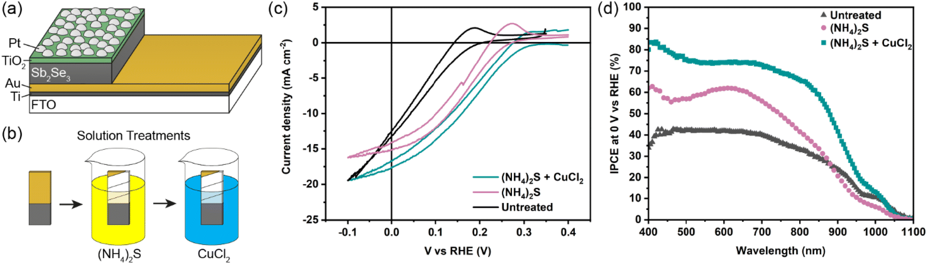 | ||
| Fig. 1 (a) A schematic showing the device configuration of Sb2Se3 photocathodes. All samples have an FTO/Ti/Au/Sb2Se3/TiO2/Pt configuration. The difference lies in the treatments undertaken before the TiO2/Pt layer deposition. (b) A schematic showing the (NH4)2S and CuCl2 treatment processes. Before the TiO2/Pt layers were deposited, the samples were wrapped in Teflon tape and etched/treated sequentially with (NH4)2S and CuCl2 solutions. (c) Current density vs. voltage plots of a typical sample in 1 M H2SO4 under simulated 1 sun illumination. (d) Quantum efficiency spectra in 1 M H2SO4 at 0 V vs. RHE under 1% sun-white light bias. | ||
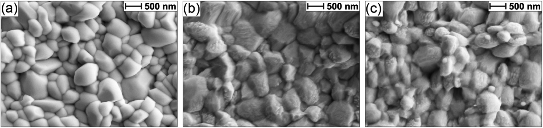 | ||
| Fig. 2 SEM images for an FTO/Ti/Au/Sb2Se3 sample (a) untreated, (b) etched via (NH4)2S, and (c) etched via (NH4)2S + CuCl2 treatment. | ||
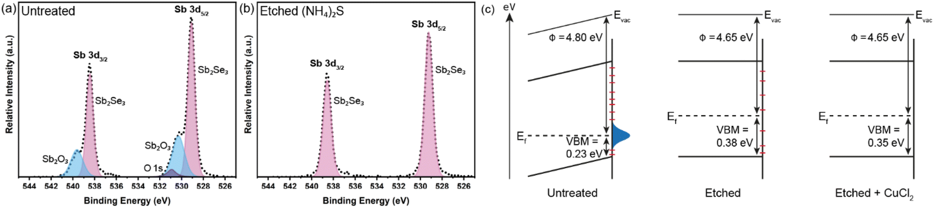 | ||
| Fig. 3 Synchrotron-based XPS core level spectra of Sb 3d for (a) untreated Sb2Se3 and (b) Sb2Se3 etched with (NH4)2S. (c) Band alignment changes due to the Sb2O3 layer (represented by the blue Gaussian) and surface states (represented by red dashes), measured by KP-FM and XPS valence band maxima (VBM). Band bending is represented as a sloping line due to the low doping (the space charge region is larger than the film thickness). | ||
Transmission electron microscopy (TEM) was used to closely observe the grains and grain boundaries for the three sample types. Fig. S8–S10† clearly show the distribution of elements, local structure, and crystallinity of different layers in these devices. However, no significant differences were observed between the three samples. EDX measurements following TEM were also undertaken in order to detect S or Cu near the surface or in the grain boundaries. Again, no significant differences were obtained from the EDX data. In Fig. S11,† a line scan passing through two Sb2Se3 grains and a grain boundary revealed a striking homogeneity of Sb, Se, Cu and Cl across grain boundaries, indicating that the amount of each element does not vary significantly throughout. This suggests that Cu does not tend to accumulate within the grain boundaries, contrary to the previous study showing the grain boundary inversion effect by the CuCl2 treatment on Sb2Se3.26 To detect the low amount of S and Cu on the surface, time of flight mass spectrometry (ToF-SIMS) was employed. From Fig. 4a, a substantial S signal is observed after the etching step and remains on the surface even after the CuCl2 treatment. The Cu content also increases after the CuCl2 treatment, as seen in Fig. 4b. Some Cu penetrates even further into the film; whilst this may be due to experimental noise, it may also be indicative of an exceedingly small amount of Cu making a bond with sublayer atoms. This behaviour is seen during DFT simulations and will be explained further in the next section. Both the S and the Cu content are highest at the surface. This coincides well with the lower amount of Sb and Se on the surface as opposed to the bulk (Fig. 4c). Similarly, from Fig. 4d, it can be observed that the CuCl2 treatment prevents the reoxidation of the photo absorber surface, allowing for a better interface with TiO2 as antimony oxide amounts on the surface also decrease and remain low after the etching treatment. Chloride content appears in all three films, which indicates that it may be present as a contaminant in the precursors from which the Sb2Se3 is synthesised or from exposure to air prior to the measurement (Fig. S12†). Regardless, as chlorine has not been detected by any other methods and does not appear to have any effect when films are treated with other Cl sources, it can be concluded that Cl does not bind with or otherwise integrate into Sb2Se3. This is in agreement with the literature in which chlorine is known to have a high formation enthalpy for interstitial doping, and the temperatures in this treatment are insufficient for the substitutional doping of this element into the Sb2Se3 thin films.19 Previous experimental studies also show that Cl ions tend to stay at the surface and not diffuse into the film. This is likely due to their large ion radius of 1.81 Å and electrostatic repulsive force, which can account for their negligible effects on device performance.
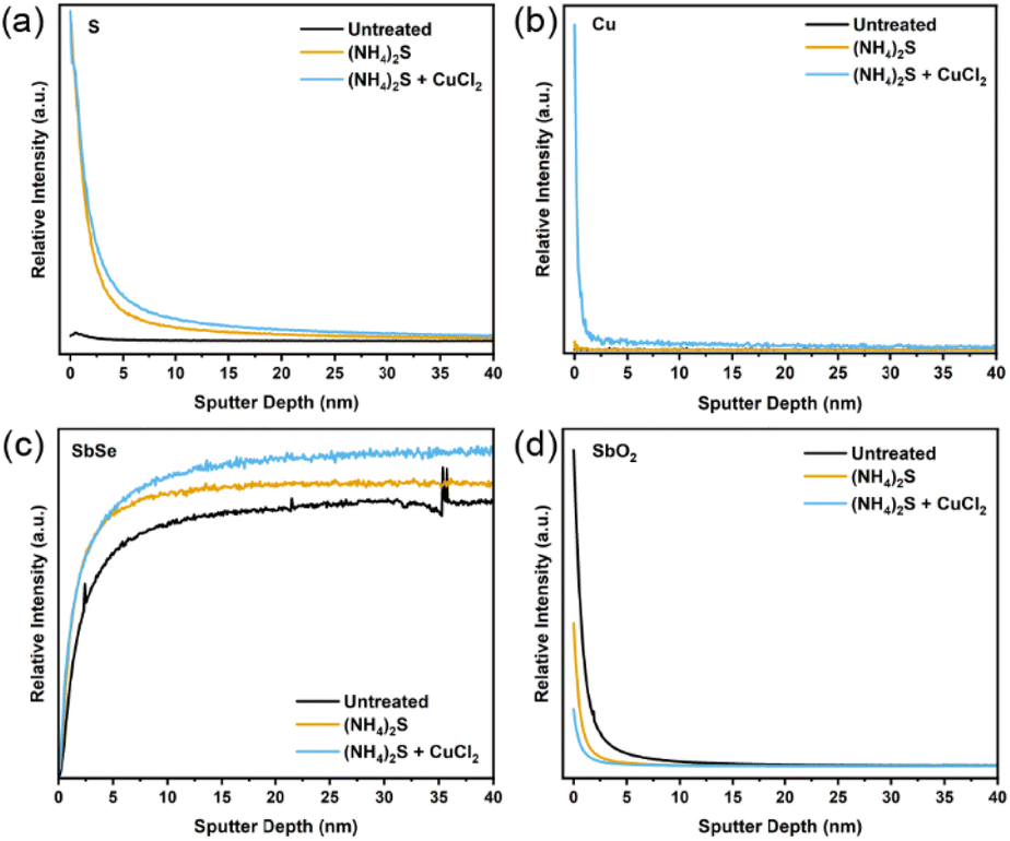 | ||
| Fig. 4 ToF-SIMS sputter depth profile for (a) sulphur, (b) copper, (c) antimony selenide, (d) antimony oxide. | ||
Spin-polarised DFT-MD was employed to shed light on the mechanism of action of the treatments. The (001) Sb2Se3 surface was chosen as a suitable simplified representation of the surface of the polycrystalline films due to the preferential (hkl) orientation observed by XRD. The (001) Sb2Se3 crystal was modelled where the ribbons had been cut, resulting in dangling bonds (Fig. 5a). 16 Cu ions were placed at the interface with the (001) Sb2Se3, and DFT-MD was performed at a temperature of 150 °C, which is the maximum temperature of the ALD chamber; the next synthesis step of these thin films. Analysing a 40 ps long DFT-MD trajectory, it was found that all the interfacial Cu ions moved towards the surface, making covalent bonds with the (001) Sb2Se3 surface. In particular, all Cu ions are surface adsorbed, making (on average) 2 bonds with Se surface atoms at a distance of 2.3 Å as highlighted by the first peak position of the radial distribution function between surface Se atoms and Cu ions in Fig. 5b. Cu ions become coordinatively saturated once adsorbed at the surface, finding their ‘equilibrium’ position.
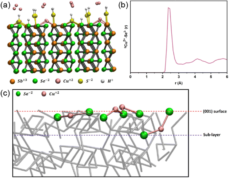 | ||
| Fig. 5 (a) Zoom-in view of the simulation box: (001) Sb2Se3 at the interface with 16 Cu atoms. Each Sb surface atom is terminated by S–H, and some Se surface atoms are terminated by hydrogen atoms (see text for details). Antimony atoms are presented in orange, and selenium atoms are in green. Sulphur atoms in yellow and hydrogen in white colour, respectively. (b) Radial distribution function between surface Se atoms and Cu ions. (c) Average position of Cu ions (in pink colour) during the simulation time. | ||
The temperature of 150 °C does not seem to be enough to break Cu–Se surface bonds and drive Cu ions into the Sb2Se3 structure (channels). The average position of the bound Cu ions during the DFT-MD simulation has been found at the level of the (001) Sb2Se3 surface, which involves a local distortion into the regular crystalline geometry of the (001)-surface pattern. However, during the DFT-MD, only one Cu atom (out of the 16 Cu atoms placed initially at the interface) positions itself between the (001) surface and the sublayer of the solid structure, evidencing a slightly more penetrating behaviour (binding to one surface Se atom and one sublayer Se atom) as shown in Fig. 5c. Although this could be ascribed to Cu-motion (‘fluctuations’) around the equilibrium position at the surface, it would be in line with the ToF-SIMS measurements where Cu atoms have been observed in the outermost layers of the slab. The calculation showed that Cu ions could bind to the Se ions at the (001) surface of Sb2Se3. Together with the experimental observations, in which the performance was enhanced by the CuCl2 treatment with favourable band bending, it implies that forming the Cu–Se bonds can passivate the detrimental surface states.
3. Experimental
3.1 Synthesis of Sb2Se3 photocathode
The FTO TEC 15 substrates from Pilkington were cleaned by consecutive washing in water and ethanol in an ultrasonic bath and treated for 30 minutes under UV/ozone to remove surface contaminants. 10 nm of Ti adhesion layer and 150 nm of Au were coated onto the FTO substrates using a Safematic CCU-010 sputter coater. In a three-electrode configuration, Sb metal was electrodeposited on top of the FTO/Ti/Au substrates. The Sb solution (100 mL) consisting of 15 mM potassium antimony tartrate K2Sb2(C4H2O6)2 (Sigma-Aldrich, ≥99%) and 50 mM tartaric acid (Acros Organics, 99.5%) was adjusted to a pH of 1.3 (pH adjusted using conc. sulfuric acid, (Sigma-Aldrich, ≥99%)). To electrodeposit the Sb, a potential of −0.3 V vs. Ag/AgCl was applied, and the thickness of the Sb metal was controlled by limiting the charge passed to 1.4 C cm−2.14,29 A two-zone furnace was used to selenise the electrodeposited Sb substrate. 30 mg of selenium pellets were placed symmetrically around the Sb substrate, and the chamber was purged with argon. A ramping rate of 15 °C min−1 was used to reach 350 °C, and the sample was held at this temperature for 40 min under static argon. After this 60 minute procedure, the furnace lid was opened to cool down the tube to room temperature, requiring approximately 60 minutes. After the selenisation, the exposed area of the Au layer (i.e., where Sb was not deposited) remains the same colour and is still conductive, indicating that the Au layer is stable during this process. This simple synthesis method enables the fabrication of high-quality compact thin films without requiring sophisticated high vacuum equipment. However, small leaks in the gas connection to the tube may cause a Sb2O3 layer to form on top of the Sb2Se3. Also, the selenisation process converts Sb metal to Sb2Se3, and therefore some unreacted Sb metal may remain in the final photoabsorber layer. This largely differs from other methods directly using a Sb2Se3 precursor. When using this electrodeposition-based method, the designated deposition area must be closely monitored in order to have reproducible thickness and performance. A 100 nm thick layer of TiO2 was deposited via atomic layer deposition (ALD) using a Picosun R200 system. Ti and O were sourced from tetrakis(dimethylamido)titanium (TDMAT), and H2O. The temperature of the TDMAT precursor cylinder was held at 85 °C, and the reactor temperature at 120 °C. The thickness of the TiO2 layer was confirmed by ellipsometry on a silicon witness wafer. In a final step, a nominally 2 nm thick layer of Pt was sputtered onto the photocathode.3.2 Solution treatments
The exposed Au surface was protected with Teflon tape before all treatments. The Sb2Se3 thin films were dipped for 5 s into a clear yellow aqueous (NH4)2S solution (Sigma-Aldrich, 40–48 wt% in H2O) (10 mL, 10–12 wt%) at room temperature, then rinsed for 10 s with distilled water and dried under N2 flow. The CuCl2 treatment was undertaken following the etching procedure. Films were dipped for 5 min into a clear dark blue aqueous CuCl2 (Aldrich, 99%, powder) solution (10 mM in 28–30% in aqueous NH3) at room temperature. Subsequently, the samples were rinsed with distilled water for 10 s and dried under N2 flow. The MgCl2 (Sigma-Aldrich, anhydrous for synthesis), CsCl (Sigma-Aldrich, 99.9%) and Cu(NO3)2 (Merck, Supelco, for analysis) solutions used for control experiments were prepared with the same concentration and solvent as the CuCl2 solution (10 mM in 28–30% aqueous NH3). These treatments were likewise applied following the (NH4)2S etching step. As evident in Fig. S3a,† this quick dipping treatment at room temperature does not require further annealing or other energy-intensive equipment. The treatment solutions are also aqueous and non-toxic (as opposed to other etchants such as HF), making them simple to prepare and handle.3.3 Photoelectrochemical (PEC) characterisation of Sb2Se3
The photoelectrochemical performance of the photocathodes was measured in a three-electrode configuration using a BioLogic SP-200 potentiostat under irradiation from simulated AM 1.5G illumination, calibrated using a silicon diode from PV Measurements, Inc. (100 mW cm2). A 1 M H2SO4 (pH 0) solution was used for the measurements. The three-electrode configuration consisted of an Ag/AgCl (3 M KCl) reference electrode, a freshly cleaned Pt wire as the counter electrode and the photocathode as the working electrode. The CV was always measured with a scan speed of 10 mV s−1 and scans were performed from positive to negative to positive potential. The photocathode area was defined by epoxying (Loctite 9461) around an O-ring (ID 7 mm) that was placed on the sample surface (Fig. S13†). IPCE was measured on a home built IPCE system featuring a halogen light source with a double monochromator and a white light bias from LED. The IPCE was measured in a three-electrode configuration as above at 0 V vs. RHE at 5 nm wavelength intervals and 1% white light bias.3.4 Morphology and crystal characterisation
The plan view scanning electron microscopy (SEM) images of Sb2Se3 thin films were measured using a Zeiss Gemini 450 SEM. X-ray diffraction (XRD) was obtained using the Rigaku Smartlab diffractometer. The Sb2Se3 and Au reference cards were obtained from the Cambridge Crystallographic Data Centre (CCDC) database.3.5 TEM and FIB sample preparation
TEM lamellae were prepared by FIB (Helios 5 UX, Thermo Fischer Scientific) using AutoTEM 5 (Thermo Fischer Scientific). Carbon deposition was used to protect the surface. The chunk milling and lamellae thinning were done at 30 kV with an FIB current from 20 nA to 90 pA. Then the lamellae were polished at 5 kV and finished at 2 kV. TEM characterisation was performed on a TEM (Talos F200X, Thermo Fischer Scientific) operating at 200 kV. EDS mapping was acquired by using quadrant EDS detectors (Super-X, Thermos Fisher Scientific, the Netherlands) in STEM mode.3.6 XPS
Synchrotron XPS data (Fig. 3a and b) were acquired at the PHOENIX I (X07MB) beamline at the Swiss Light Source using an end station.30 The spectra were acquired in a high vacuum (>1 × 10⁻⁵ Pa) using a photon energy of 4000 eV and a pass energy of 100 eV. The energy scale was calibrated using an Au reference sample, setting the Au 4f7/2 line to 84.0 eV. XPS depth profiling was conducted using a Physical Electronics (PHI) Quantum 2000 X-ray photoelectron spectrometer featuring monochromatic Al-Ka radiation generated from an electron beam operated at 15 kV and 32.3 W. The energy scale of the instrument was calibrated using an Au reference sample. The analysis was conducted at 1 × 10⁻⁶ Pa, with an electron take-off angle of 45° and a pass energy of 23.50 eV. The neutraliser was set to automatic. In both cases, surface elemental concentrations were determined from the photoelectron spectra after Shirley background subtraction using the instrument-specific sensitivity factors for calculation. As necessary, the core level spectra were plotted to deconvolute spectra with contributions from multiple elements. An asymmetric line shape (GL 30) was assumed for the core level emissions with a separation of ΔE = 9.34 eV for the Sb 3d doublet.3.7 KP-FM
An Asylum Research AFM (MFP-3D) was used to measure the work function of the samples. The probe used for the measurement was an AC240TM-R3. For calibration of the work function of the tip, a highly ordered pyrolytic graphite (HOPG) was used, with a reported work function of ∼4.6 eV.31 To achieve a fresh HOPG surface, a piece of scotch tape was used to pull off a few top layers of the graphite, exposing a fresh, clean surface for calibration. The HOPG used was purchased from MikroMasch (Grade: ZYA).The open-source Gwyddion software package and the Asylum Research built-in software were used to analyse the AFM pictures further and determine the average work function of the surface.
3.8 ToF-SIMS
Secondary ion mass spectrometry measurements were conducted on a ToF-SIMS.5 from IONTOF GmbH, Germany. The instrument was operated in spectroscopy mode, and Bi+ primary ions with an energy of 25 keV were used to analyse an area of 500 × 500 μm2. Sputtering was carried out with caesium ions with an energy of 500 V. The sputtering time was correlated with sputter depth by measuring the sputtered area with a Dektak Stylus Profilometer (Bruker, Germany).3.9 Computational
Spin-polarized DFT-MD simulation was performed in the Born–Oppenheimer framework employing the CP2K program package on (001) Sb2Se3 at the interface with 16 Cu atoms.32,33 8 Cu atoms are initially placed at around 3 Å distance from the (001) surface, and 8 Cu atoms are initially placed at the height of the (001) surface. The (001) Sb2Se3 slab consists of 240 atoms, where each Sb surface atom is terminated by S–H (some S–H are bridging two surface Sb atoms), and each Se atom is terminated by hydrogen atoms, as shown in Fig. 5a side view and in Fig. S14a† top view. The simulation box dimensions are x = 23.24 Å, y = 23.54 Å and z = 40.0 Å. Periodic boundary conditions (PBCs) are applied in all 3-directions of space. A vacuum of around 15 Å has been inserted to separate the periodic z-replicas. The atoms were described by GTH pseudopotentials. The Perdew–Burke–Ernzerhof (PBE) exchange–correlation function was employed in agreement with previous works, which have shown a good description of the properties of Sb2Se3.19,34–36 The DZVP-MOLOPT-SR basis set and a 400 Ry plane wave basis set for all atoms have been used, being a good compromise between computational cost and accuracy.37 Grimme's D3 dispersion correction was employed.19,38,39 The DFT-MD simulation was performed for ∼40 ps in the NVT ensemble at a temperature of 150 °C (Nosé–Hoover chain thermostat) and adopted the Velocity-Verlet algorithm with a time step of 0.5 fs.40,41 A uniform background charge and the Ewald summation for electrostatics take care of the total charge of the simulation box whenever necessary, as a standard procedure in DFT-MD simulations. The PBE functional was supplemented with the Hubbard U parameter in order to overcome the self-interaction error in the exchange and correlation of the over delocalized d- and f-orbitals (and the consequent underestimation of the Sb2Se3 band gap).42–45 Hubbard parameter U is known as the on-site Coulomb interaction energy.45U parameters have been calculated for Sb3+ and Se2− atoms in order to reproduce the experimental band gap energy of around 1.2 eV of Sb2Se3. Values of U = 3 eV, U = 2 eV have been calculated and adopted for Sb3+ and Se2− atoms, respectively. See ESI and Fig. S14 and S15† for modelling of the bulk crystalline structure of Sb2Se3 and for bulk structural, electronic and mechanical properties calculations.4. Conclusions
This study demonstrates enhanced photovoltage and photocurrent improvements through low-cost and room-temperature surface modification treatments. Overall, the etching treatment with (NH4)2S + CuCl2 on the surface of the Sb2Se3 in substrate configuration improved the onset potential by 57% and the current density by 38%. This progressive improvement is due to the removal of the surface Sb2O3 layer on the surface after the etching treatment. This is firmly evidenced by XPS. This layer appears to cause an unfavourable surface band bending, causing surface recombination. Further improvement was also observed after CuCl2 solution treatment due to the binding of Cu to surface Se atoms which passivate the surface defects present on the surface of the material as a result of dangling bonds. The binding of Cu can be seen through ToF-SIMS and is supported by DFT calculations. As the stability, the light dependency and therefore the performance of the devices depends on the catalyst, further investigation can be done to address the loss of the catalyst itself and improve its durability. Despite the considerable improvement in the photovoltage via these simple surface treatments, there is still a significant loss of photovoltage due to bulk defects such as cation–anion antisite defects.46 Therefore, a better understanding and screening of other metal halides and nitrates, combined with our previously studied bulk passivation methods,47 could pave the way towards improved performance in Sb2Se3 photocathodes.Author contributions
S. D. T. and P. A. designed the experiment. W. Y. provided supervision and advice. P. A. fabricated and tested all the devices. F. C. undertook the DFT calculations. T. M. carried out the KP-FM and light intensity dependant measurements. R. C. and P. Z. performed the ToF-SIMS and FIB-TEM measurements, respectively. Z. N. operated and measured the XPS end station at the Swiss light source (SLS). S. L. provided supervision for the DFT calculations.Conflicts of interest
There are no conflicts to declare.Acknowledgements
This work was supported by the University of Zurich, URPP LightChEC, and SNF Project # 184737. P. A. thanks Jan Bühler for the figure designs and editing in this publication and Zhenbin Wang for the XRD measurement. We thank Selim Kazaz, Levin Häfliger, Thierry Eberhard, and Bernhard Fenner for preliminary studies. Z. N. acknowledges the PHOENIX I (X07MB) beamline of the Swiss Light Source, Paul Scherrer Institute, Villigen-PSI, Switzerland. This work was supported by a grant from the Swiss National Supercomputing Centre (CSCS) under project ID s1001. P. Z. acknowledge ScopeM for the support.Notes and references
- M. G. Walter, E. L. Warren, J. R. McKone, S. W. Boettcher, Q. Mi, E. A. Santori and N. S. Lewis, Chem. Rev., 2010, 110, 6446–6473 CrossRef CAS PubMed.
- W. Yang, J. H. Kim, O. S. Hutter, L. J. Phillips, J. Tan, J. Park, H. Lee, J. D. Major, J. S. Lee and J. Moon, Nat. Commun., 2020, 11, 861 CrossRef CAS PubMed.
- M. B. Costa, F. W. S. Lucas, M. Medina and L. H. Mascaro, ACS Appl. Energy Mater., 2020, 3, 9799–9808 CrossRef CAS.
- Y. Wang, R. Tang, L. Huang, C. Qian, W. Lian, C. Zhu and T. Chen, ACS Appl. Mater. Interfaces, 2022, 14, 33181–33190 CrossRef CAS.
- K. Sivula and R. van de Krol, Nat. Rev. Mater., 2016, 1, 15010 CrossRef CAS.
- R. Sathre, C. D. Scown, W. R. Morrow, J. C. Stevens, I. D. Sharp, J. W. Ager, K. Walczak, F. A. Houle and J. B. Greenblatt, Energy Environ. Sci., 2014, 7, 3264–3278 RSC.
- K. Zeng, D.-J. Xue and J. Tang, Semicond. Sci. Technol., 2016, 31, 063001 CrossRef.
- Y. Ma, B. Tang, W. Lian, C. Wu, X. Wang, H. Ju, C. Zhu, F. Fan and T. Chen, J. Mater. Chem. A, 2020, 8, 6510–6516 RSC.
- Y. Zhou, L. Wang, S. Chen, S. Qin, X. Liu, J. Chen, D.-J. Xue, M. Luo, Y. Cao, Y. Cheng, E. H. Sargent and J. Tang, Nat. Photonics, 2015, 9, 409–415 CrossRef CAS.
- R. E. Williams, Q. M. Ramasse, K. P. McKenna, L. J. Phillips, P. J. Yates, O. S. Hutter, K. Durose, J. D. Major and B. G. Mendis, ACS Appl. Mater. Interfaces, 2020, 12, 21730–21738 CrossRef CAS.
- Y. Zhou, M. Leng, Z. Xia, J. Zhong, H. Song, X. Liu, B. Yang, J. Zhang, J. Chen, K. Zhou, J. Han, Y. Cheng and J. Tang, Adv. Energy Mater., 2014, 4, 1301846 CrossRef.
- Z. Li, X. Liang, G. Li, H. Liu, H. Zhang, J. Guo, J. Chen, K. Shen, X. San, W. Yu, R. E. I. Schropp and Y. Mai, Nat. Commun., 2019, 10, 125 CrossRef.
- X. Wang, R. Tang, C. Jiang, W. Lian, H. Ju, G. Jiang, Z. Li, C. Zhu and T. Chen, Adv. Energy Mater., 2020, 10, 2002341 CrossRef CAS.
- R. R. Prabhakar, W. Septina, S. Siol, T. Moehl, R. Wick-Joliat and S. D. Tilley, J. Mater. Chem. A, 2017, 5, 23139–23145 RSC.
- C. Chen, W. Li, Y. Zhou, C. Chen, M. Luo, X. Liu, K. Zeng, B. Yang, C. Zhang, J. Han and J. Tang, Appl. Phys. Lett., 2015, 107, 043905 CrossRef.
- L. J. Phillips, C. N. Savory, O. S. Hutter, P. J. Yates, H. Shiel, S. Mariotti, L. Bowen, M. Birkett, K. Durose, D. O. Scanlon and J. D. Major, IEEE J. Photovolt., 2019, 9, 544–551 Search PubMed.
- A. Mavlonov, T. Razykov, F. Raziq, J. Gan, J. Chantana, Y. Kawano, T. Nishimura, H. Wei, A. Zakutayev, T. Minemoto, X. Zu, S. Li and L. Qiao, Sol. Energy, 2020, 201, 227–246 CrossRef CAS.
- C. N. Savory and D. O. Scanlon, J. Mater. Chem. A, 2019, 7, 10739–10744 RSC.
- A. Stoliaroff, A. Lecomte, O. Rubel, S. Jobic, X. Zhang, C. Latouche and X. Rocquefelte, ACS Appl. Energy Mater., 2020, 3, 2496–2509 CrossRef CAS.
- C. Chen and J. Tang, ACS Energy Lett., 2020, 5, 2294–2304 CrossRef CAS.
- W. Yang, R. R. Prabhakar, J. Tan, S. D. Tilley and J. Moon, Chem. Soc. Rev., 2019, 48, 4979–5015 RSC.
- N. Guijarro, M. S. Prévot and K. Sivula, Phys. Chem. Chem. Phys., 2015, 17, 15655–15674 RSC.
- M. Buffière, A.-A. El Mel, N. Lenaers, G. Brammertz, A. E. Zaghi, M. Meuris and J. Poortmans, Adv. Energy Mater., 2015, 5, 1401689 CrossRef.
- J. Debehets, P. Homm, M. Menghini, S. A. Chambers, C. Marchiori, M. Heyns, J. P. Locquet and J. W. Seo, Appl. Surf. Sci., 2018, 440, 386–395 CrossRef CAS.
- H. Aibin, W. Wenwu and X. Qiuxia, J. Semicond., 2009, 30, 084001 CrossRef.
- C. Chen, K. Li, S. Chen, L. Wang, S. Lu, Y. Liu, D. Li, H. Song and J. Tang, ACS Energy Lett., 2018, 3, 2335–2341 CrossRef CAS.
- C. H. Don, H. Shiel, T. D. C. Hobson, C. N. Savory, J. E. N. Swallow, M. J. Smiles, L. A. H. Jones, T. J. Featherstone, P. K. Thakur, T.-L. Lee, K. Durose, J. D. Major, V. R. Dhanak, D. O. Scanlon and T. D. Veal, J. Mater. Chem. C, 2020, 8, 12615–12622 RSC.
- H. Shiel, T. D. C. Hobson, O. S. Hutter, L. J. Phillips, M. J. Smiles, L. A. H. Jones, T. J. Featherstone, J. E. N. Swallow, P. K. Thakur, T.-L. Lee, J. D. Major, K. Durose and T. D. Veal, J. Appl. Phys., 2021, 129, 235301 CrossRef CAS.
- W. Septina, S. Ikeda, Y. Iga, T. Harada and M. Matsumura, Thin Solid Films, 2014, 550, 700–704 CrossRef CAS.
- Z. Novotny, D. Aegerter, N. Comini, B. Tobler, L. Artiglia, U. Maier, T. Moehl, E. Fabbri, T. Huthwelker, T. J. Schmidt, M. Ammann, J. A. van Bokhoven, J. Raabe and J. Osterwalder, Rev. Sci. Instrum., 2020, 91, 023103 CrossRef CAS.
- M. M. Beerbom, B. Lägel, A. J. Cascio, B. V. Doran and R. Schlaf, J. Electron Spectrosc. Relat. Phenom., 2006, 152, 12–17 CrossRef CAS.
- J. Hutter, M. Iannuzzi, F. Schiffmann and J. Vandevondele, Wiley Interdiscip. Rev.: Comput. Mol. Sci., 2014, 4, 15–25 CAS.
- J. Vandevondele, M. Krack, F. Mohamed, M. Parrinello, T. Chassaing and J. Hutter, Comput. Phys. Commun., 2005, 167, 103–128 CrossRef CAS.
- J. P. Perdew, K. Burke and M. Ernzerhof, Phys. Rev. Lett., 1996, 77, 3865–3868 CrossRef CAS PubMed.
- S. Goedecker, M. Teter and J. Hutter, Phys. Rev. B: Condens. Matter Mater. Phys., 1996, 54, 1703–1710 CrossRef CAS PubMed.
- R. Vadapoo, S. Krishnan, H. Yilmaz and C. Marin, Phys. Status Solidi B, 2011, 248, 700–705 CrossRef CAS.
- J. VandeVondele and J. Hutter, J. Chem. Phys., 2007, 127, 114105 CrossRef.
- J. Moellmann and S. Grimme, J. Phys. Chem. C, 2014, 118, 7615–7621 CrossRef CAS.
- L. Goerigk, in Non-Covalent Interactions in Quantum Chemistry and Physics, Elsevier, 2017, pp. 195–219 Search PubMed.
- D. J. Evans and B. L. Holian, J. Chem. Phys., 1985, 83, 4069–4074 CrossRef CAS.
- L. Verlet, Phys. Rev., 1967, 159, 98–103 CrossRef CAS.
- C. Loschen, J. Carrasco, K. M. Neyman and F. Illas, Phys. Rev. B, 2007, 75, 035115 CrossRef.
- J. Hubbard, Proc. R. Soc. London, Ser. A, 1963, 276, 238–257 Search PubMed.
- S. A. Tolba, K. M. Gameel, B. A. Ali, H. A. Almossalami and N. K. Allam, in Density Functional Calculations - Recent Progresses of Theory and Application, InTech, 2018 Search PubMed.
- V. I. Anisimov, J. Zaanen and O. K. Andersen, Phys. Rev. B, 1991, 44, 943–954 CrossRef CAS PubMed.
- C. N. Savory and D. O. Scanlon, J. Mater. Chem. A, 2019, 7, 10739–10744 RSC.
- R. R. Prabhakar, T. Moehl, D. Friedrich, M. Kunst, S. Shukla, D. Adeleye, V. H. Damle, S. Siol, W. Cui, L. Gouda, J. Suh, Y. R. Tischler, R. van de Krol and S. D. Tilley, Adv. Funct. Mater., 2022, 32, 2112184 CrossRef CAS.
Footnote |
| † Electronic supplementary information (ESI) available. See DOI: https://doi.org/10.1039/d3ta00554b |
| This journal is © The Royal Society of Chemistry 2023 |