
 Open Access Article
 This Open Access Article is licensed under a
 Creative Commons Attribution 3.0 Unported Licence
Tungsten dichalcogenide WS2xSe2−2x films via single source precursor low-pressure CVD and their (thermo-)electric properties†
V.
Sethi
 a,
D.
Runacres
b,
V.
Greenacre
b,
Li
Shao
b,
A. L.
Hector
b,
W.
Levason
b,
C. H.
de Groot
a,
G.
Reid
*b and
R.
Huang
*a
a,
D.
Runacres
b,
V.
Greenacre
b,
Li
Shao
b,
A. L.
Hector
b,
W.
Levason
b,
C. H.
de Groot
a,
G.
Reid
*b and
R.
Huang
*a
aSchool of Electronics and Computer Science, University of Southampton, Southampton, SO17 1BJ, UK. E-mail: r.huang@soton.ac.uk
bSchool of Chemistry, University of Southampton, Southampton, SO17 1BJ, UK. E-mail: G.Reid@soton.ac.uk
First published on 3rd April 2023
Abstract
Semiconducting transition metal dichalcogenides have gained increased interest as potential alternatives to graphene due to their tunable electronic bandgaps. In this study, we present the deposition of stoichiometric WS2xSe2−2x (0 ≤ x ≤ 1) binary and ternary thin films using the single source precursors, [WECl4(E′nBu2)] (E = S or Se; E′ = S or Se), via low-pressure chemical vapour deposition. Compositional and structural characterisations of the deposits have been performed by grazing-incidence X-ray diffraction, scanning electron microscopy, X-ray photoelectron spectroscopy, and Raman spectroscopy, confirming the phase purity and stoichiometry. Electrical characterisation via Hall measurements reveals high electrical conductivities for those films. Such high conductivity is likely related to Se and S vacancies in the films and can be tuned through an annealing process. The thermoelectric capabilities of the WS2xSe2−2x have been characterised with the use of variable-temperature Seebeck measurements, showing a peak power factor of 6 μW m−1 K−2 for the as-deposited WS2 film at 553 K.
1. Introduction
The discovery of graphene's extraordinary electrical properties has paved the way for faster and more efficient electronic devices. However, the absence of an electronic bandgap hinders potential applications.1 The inorganic analogues of graphene, layered transition metal dichalcogenides (TMDCs), ME2 (M = Nb, Ta, Mo, W, V, etc.; E = S, Se, or Te) do possess an electronic band gap with the magnitude and specific electronic properties dependent on the choice of metal and chalcogen. These unique semiconducting properties have attracted tremendous interest to explore TMDCs for the next generation of electrical and optical devices.2Among the family of TMDCs, tungsten-based dichalcogenides (e.g. WS2, WSe2, WS2xSe2−2x) are of interest due to the natural abundance of W in the earth's crust, low-toxicity and cost-effectiveness.3,4 These advantages have recently gained increased attention within the field of Li-ion batteries where WS2 and WSe2 have been identified as potential anode materials. However, integration has been hindered by intrinsically low electrical conductivities, making highly conductive WS2 and WSe2 of great interest.5–7 The fabrication of atomically thin monolayered films of these materials lends itself to integration into transistor-based devices, with the tuning of electrical performance allowing control of the on-off bias of these devices, as well as a reduction in quantum tunnelling effects.8,9 The ability to tune the electronic performance of these materials also benefits a multitude of optoelectronic applications, including photodetectors and light-emitting diodes, which allows for the tailoring of devices for specific photoelectronic applications.10,11
Thin-film TDMCs can be grown via various approaches, including mechanical/liquid exfoliation,12,13 sputtering,14 pulsed layer deposition,15 atomic layer deposition,7 and molecular beam epitaxy.16 The preparation of binary WE2 (E = S, Se) thin films is usually achieved by sulfurization or selenization of WO3 thin films, followed by an annealing process.17,18 Chemical vapour deposition (CVD) is a low-cost and versatile deposition technique for semiconductor alloys. It is widely used in industry with most processes using dual or multiple precursor sources, each of which delivers one of the required elements. Several CVD approaches have been employed for the deposition of binary or ternary tungsten-based TMDCs, most of which use precursor sources such as WF6 + H2S; or WCl6, WOCl4 or W(CO)6 with thiols.19–32 In addition, aerosol-assisted CVD (AACVD) of WS2 from the dithiocarbamate complex [WS(S2)(S2CNEt2)2], and of Mo1−xWxS2 from a mixture of [WS(S2)(S2CNEt2)2] and [Mo(S2CNEt2)4] have been reported.33,34
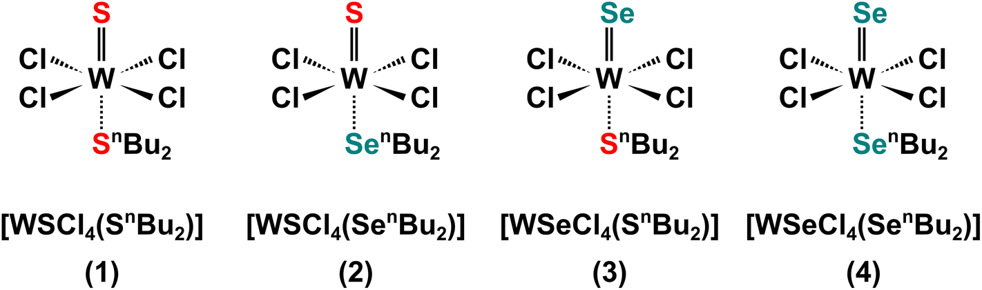
Compared with dual/multiple source precursors, single source precursors (SSPs), which contain the metal and chalcogen(s) within a single molecule can potentially offer better control of deposit stoichiometry, cost-effective use of reagents, easier-to-handle precursors and, in some cases, the ability to selectively deposit the chalcogenides onto nano-patterned substrates.35 We recently reported the first single source low-pressure CVD reagent for WS2, the dinuclear [(WSCl4)2(iPrSCH2CH2SiPr)].36 This success was very encouraging given the high molecular weight of the complex. Although the films produced were of good quality, we noted that a considerable residue remained after the vaporisation of the reagent, and deposition occurred only over a limited area of the substrate. We, therefore, sought to develop a new reagent that would maintain or improve the film quality, deposit more evenly and continuously over a larger substrate area, and which would vaporise completely under the experimental conditions. W(VI) complexes of monothioethers could be a potential option. However, the only known example, [WSCl4(SMe2)],36 is unsuitable since it lacks a low energy decomposition route, hence we considered complexes containing thioethers with longer alkyl chains, specifically containing β-hydrogen atoms. In previous work on other metal sulfide materials, including Nb,22,37 Sn38 and Mo,39 we found that precursors incorporating thioethers with n-butyl substituents proved particularly suitable. The nBu group offers a β-hydride elimination route, and its complexes are often low melting or waxy solids, implying low lattice energies that aid vaporisation. SnBu2 is also cheap and commercially available. Recently, we have shown that [WSeCl4(SenBu2)] is a suitable precursor for growth of WSe2 thin films via CVD.40
We report here the development and application of new, tailored mononuclear complexes, [WECl4(E′nBu2)] (E = S, Se; E′ = S, Se), designed as single source precursors for the low-pressure CVD (LPCVD) growth of tungsten dichalcogenides. By selecting the different combinations of E and E′ in the precursor, we could not only deposit thin films of the binary WS2 and WSe2, but also, for the first time, the ternary WS2xSe2−2x films. Moreover, electrical characterisation on the as-deposited WS2xSe2−2x (0 ≤ x ≤ 1) thin films reveal high electrical conductivities with an increase of several orders in carrier concentration when compared to literature.41–43 This high conductivity is likely related to the substantial number of Se and S vacancies within the films. Such high conductivity can be tuned via an annealing process to reduce the vacancy concentration. The capability of controlling the electrical conductivity of WS2xSe2−2x films via the choice of single source precursor and the annealing process can be beneficial for its application in advanced optical switches as well as transistor device mobility engineering.44–46
2. Material preparation and methods
2.1 Single source precursor synthesis
SnBu2 was purchased from Sigma-Aldrich and used as received. WSCl4,36 WSeCl4,40 and SenBu2,47 were prepared as previously described. All reactions were conducted under a dry dinitrogen atmosphere using Schlenk, vacuum line, and glovebox techniques. CH2Cl2 was dried by distillation from CaH2 and n-hexane from Na and stored over activated 4 Å molecular sieves. Dry NMR solvents were also stored over 4 Å sieves. IR spectra were recorded as Nujol mulls between CsI plates using a PerkinElmer Spectrum 100 spectrometer over the range of 4000–200 cm−1. Raman spectra used a Renishaw InVia Raman Microscope with a 100 mW He–Ne 785 nm laser. NMR spectra were recorded using a Bruker AVII 400 spectrometer. 1H NMR spectra were referenced to residual solvent resonances and 77Se{1H} NMR spectra to external neat SeMe2.2.1.1.1 [WSCl4(SnBu2)] (1). A solution of di-n-butyl sulfide (0.041 g, 0.28 mmol) in dichloromethane (5 mL) was added slowly to a suspension of WSCl4 (0.100 g, 0.28 mmol) in dichloromethane (5 mL). The dark red solution was stirred for 1 h and then reduced to dryness in vacuo, leaving a viscous red oil. IR spectrum (Nujol, ν/cm−1): 538 s (W
![[double bond, length as m-dash]](https://www.rsc.org/images/entities/char_e001.gif) S), 348 br s (W–Cl) (Fig. S1†). Raman spectrum (ν/cm−1): 535 s (WS), 379 s (W–Cl) (Fig. S2†). 1H NMR (CDCl3): 2.74 (br, [2H], CH2), 1.83 (br, [2H], CH2), 1.52 (br, [2H], CH2), 0.96 (t, [3H], CH3) (Fig. S3†).
S), 348 br s (W–Cl) (Fig. S1†). Raman spectrum (ν/cm−1): 535 s (WS), 379 s (W–Cl) (Fig. S2†). 1H NMR (CDCl3): 2.74 (br, [2H], CH2), 1.83 (br, [2H], CH2), 1.52 (br, [2H], CH2), 0.96 (t, [3H], CH3) (Fig. S3†).
2.1.1.2 [WSCl4(SenBu2)] (2). A solution of di-n-butyl selenide (0.135 g, 0.69 mmol) in dichloromethane (5 mL) was added slowly to a suspension of WSCl4 (0.250 g, 0.69 mmol) in dichloromethane (5 mL). The dark red solution was then stirred for 1 h, before the volatiles were removed in vacuo, leaving a dark red viscous oil. IR spectrum (Nujol, ν/cm−1): 533 s (W
S), 375 s (W–Cl) (Fig. S4†). Raman spectrum (ν/cm−1): 536 s (WS), 322 br (W–Cl) (Fig. S5†). 1H NMR (CD2Cl2): δ = 2.74 (br, [2H], CH2), 1.74 (br, [2H], CH2), 1.46 (br m, [2H], CH2), 0.94 (t, [3H], CH3). 77Se{1H} NMR (CD2Cl2): δ = +298.6 (s, 1JWSe = 79 Hz) (Fig. S6–S8†).
2.1.1.3 [WSeCl4(SnBu2)] (3). A solution of di-n-butyl sulfide (0.043 mL, 0.25 mmol) in dichloromethane (5 mL) was slowly added to a suspension of WSeCl4 (0.100 g, 0.25 mmol) in dichloromethane (5 mL) to form a green solution. After stirring for 10 min, the solution was concentrated in vacuo to a deep green oil. IR spectrum (Nujol, ν/cm−1): 368 s (W
Se), 343 s (W–Cl) (Fig. S9†). Raman spectrum (ν/cm−1): 379 s (WSe), 344 s (W–Cl) (Fig. S10†). 1H NMR (CD2Cl2): δ = 2.58 (br, [2H], CH2), 1.69 (br, [2H], CH2), 1.48 (br m, [2H], CH2), 0.93 (t, [3H], CH3) (Fig. S11†).
2.1.1.4 [WSeCl4(SenBu2)] (4). [WSeCl4(SenBu2)] (4) was prepared by the literature method.40
Fresh samples of single source precursors (SSPs) (1–4) were prepared just prior to the CVD experiments, as (3) and (4) in particular, tend to decompose over a period of a few hours.
A molecular representation of the SSPs (1–4) is shown in Scheme 1.
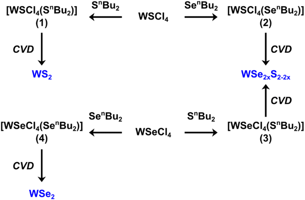 | ||
| Scheme 1 The methods used for the synthesis of precursors (1–4) and the thin film TMDC material (blue) obtained from low-pressure CVD from each. | ||
2.2 Low-pressure CVD onto fused quartz substrates
The binary and ternary TMDC films were deposited via low-pressure CVD using precursors (1–4) as shown in Scheme 1, with a schematic diagram of the CVD process provided in Fig. 1. The temperature gradient through the length of the furnace was measured using a thermocouple.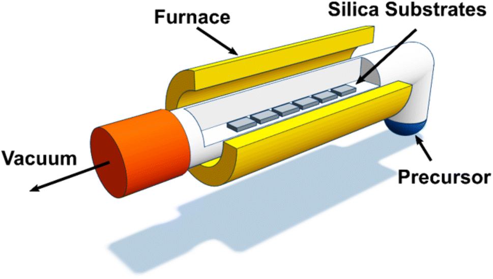 | ||
| Fig. 1 A visual representation of our low-pressure chemical vapour deposition (LPCVD) setup, consisting of an open-ended quartz tube held under vacuum to draw the volatilised precursor through the heated zone and across the silica substrates. | ||
In an N2 purged glove box the precursor (20–30 mg) was loaded into the precursor bulb at the closed end of a silica tube, silica substrates (ca. 1 × 8 × 20 mm3) were then positioned end-to-end lengthways along the tube outwards from the precursor. The tube was then set horizontally in a furnace so that the substrates were in the heated zone and the precursor protruded ca. 1 cm ((1) and (2)) or ca. 4 cm ((3) and (4)) out of the furnace. The tube was evacuated to 0.1 mmHg and the furnace was heated to 700 °C and held for 10–15 minutes to allow the temperature to stabilise. The tube was gradually moved towards the hot zone until evaporation of the precursor was observed. The position was maintained for ca. 15–20 min, or until no further evaporation occurred; negligible residue was observed in the precursor bulb. The tube was then cooled to room temperature and the substrates were removed for characterisation. Brown films were obtained from precursor (1) (actual deposition temperature range = 624–650 °C), (2) (actual deposition temperature range = 593–652 °C) and (3) (actual deposition temperature range = 563–593 °C), while silver films were obtained from precursor (4) (actual deposition temperature range = 624–650 °C) as described.40 Good film coverage over the substrate was observed for all four films with no variation of morphology over the substrate. The four films are hereafter referred to as films A, B, C and D, respectively.
2.3 WS2xSe2−2x film characterisation (0 ≤ x ≤ 1)
The WS2xSe2−2x thin films (A, B, C and D) deposited from (1–4) were characterised using a combination of techniques. The morphology was investigated by scanning electron microscopy (SEM) using a Jeol JSM 7500F FESEM with an accelerating voltage of 5 kV. X-ray diffraction (XRD) patterns were collected in grazing incidence mode (θ1 = 1°) using a Rigaku SmartLab diffractometer (Cu-Kα, λ = 1.5418 Å) with parallel X-ray beam and a Hypix detector operated in 1D mode. Phase matching and lattice parameter calculations were undertaken using the PDXL2 software package48 and diffraction patterns from ICSD.49,50 X-ray photoelectron spectroscopy (XPS) data were obtained using a Thermo Scientific Theta Probe system with Al-Kα radiation (photon energy = 1486.6 eV). All peaks are calibrated against the adventitious C 1s peak at 284.6 eV.51 All films were subject to an in situ 30 s Ar etch to remove surface oxygen prior to the measurement. Raman spectra of the deposited films were measured at room temperature on a Renishaw InVia Micro Raman Spectrometer using 532 nm excitation. The incident laser power was 0.1 mW for all samples with a 50× magnification, which resulted in a spot size of 1 μm diameter.Electrical characterisation was conducted using the van der Pauw configuration using a Nanometrics HL5500 Hall effects system across a temperature range of 150 to 450 K using liquid N2. Electrical conductivity (σ) measurements were also conducted in situ with Hall measurements to determine carrier mobility (μ) and carrier density (n) at a magnetic field of 0.5 T. A visual depiction of a typical Hall measurement is displayed in Fig. S12.† The contacts from the probes to the samples were checked carefully before each measurement. I–V curves were recorded before each measurement to ensure ohmic conduction as well as to optimise the current for a maximised voltage signal (20 mV). Variable-temperature Seebeck coefficients and electrical resistivity were measured using a JouleYacht thin-film thermoelectric parameter test system (MRS-3L). The system was calibrated using a nickel foil reference standard, and the measurement accuracy was found to be within 5%. Seebeck coefficients were determined using the differential method with a maximum temperature difference of 10 K. This system allows further extension of the electrical conductivity measurement range to ca. 550 K, as well as simultaneous measurements of thermopower.
3. Results and discussion
3.1 Composition, morphological, and structure properties
Top-view SEM images were taken to reveal the morphological properties of the four as-deposited WS2xSe2−2x films, which are shown in Fig. 2. From inspection, all four precursors yield films with continuous polycrystalline layers and slightly varying grain morphologies depending on the choice of SSP. All films have formed structures with a preferred orientation parallel to the substrate surface, reflecting the layered nature of TDMCs.52 The continuity of the films is further supported by the cross-sectional SEM images shown in Fig. S13.† EDX mappings were also conducted on all four films and are presented in Fig. S14.† It is clear that all elements are uniformly distributed, further confirming the quality of the film deposited by our SSPs.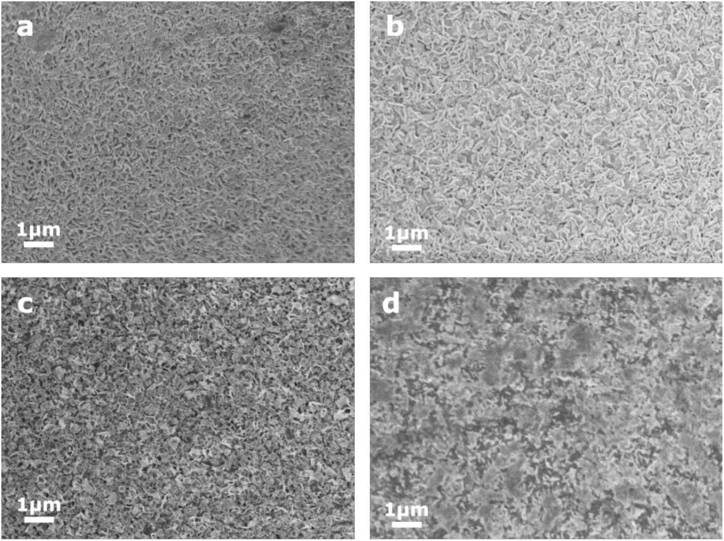 | ||
| Fig. 2 Top-view SEM images of WS2xSe2−2x films produced via low-pressure CVD using SSPs (1) to (4), respectively. | ||
The phase purity and crystallinity of the as-deposited films were examined by grazing incidence XRD analysis and are shown in Fig. 3. All films are isostructural, with no other phases detectable. The XRD patterns are consistent with the 2H coordination in space group P63/mmc which has two layers per unit cell. All films were dominated by the 002 reflections, suggesting a preferred orientation in the 〈00l〉 direction. A systematic shift of the characteristic diffraction peaks with increasing Se content is also evident as the WS2 lattice expands with the incorporation of Se into the film. For the ternary films (B and C) this peak is located between those for the binary materials, 14.3° (A: WS2) and 13.6° (D: WSe2).
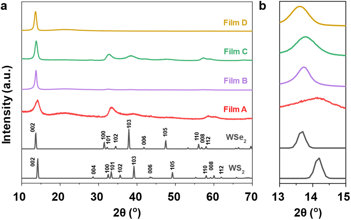 | ||
| Fig. 3 (a) Grazing incidence X-ray diffraction patterns of the as-deposited WS2xSe2−2x films from (1–4), together with reference XRD patterns for both WS2 and WSe2 (black);49,50 (b) an expansion of the range 13° and 15° to illustrate the shift of the 002 peaks. | ||
The XRD indicated our as deposited films adopt the 2H structure, but Raman can be more sensitive to structure in small crystallite materials. The 2H structure is expected to result in 18 potential phonon modes with 3 of them Raman active with A1g, E1g and E2g symmetry.53 The A1g represents the out-of-plane symmetrical stretching and the E1g and E2g modes signify the doubly degenerate asymmetric and symmetric in-plane vibrations within TMDCs, as visually depicted in Fig. 4a.53 However, in the Raman backscattering configuration used in this study, only the A1g and E2g modes can be observed due to the asymmetric stretching and the double degeneracy of the E1g modes.53 The presence of these two Raman active modes is evident in all of the as-deposited films, as seen in Fig. 4b. The characteristic peaks, namely, (i) E2g(Se–W–Se) and (ii) A1g(Se–W–Se) are located at 248.7 cm−1 and 258.5 cm−1 respectively. These are related to the WSe2 film (D from precursor (4)).54 The Raman spectra of the as-deposited WS2 film (A from precursor (1)) align well with reports from literature with peaks (iii) E2g(S–W–S) and (v) A1g(S–W–S) at 353.8 cm−1 and 418.5 cm−1 respectively, with a peak separation of 68.4 cm−1.53,55 It should be noted that the peak at ca. 350.1 cm−1 is a convolution of two modes: the aforementioned E2g(S–W–S) mode and the 2LA(M) mode. The latter of these is a second-order longitudinal acoustic phonon. This feature is often prevalent in monolayer and few-layer WS2.56
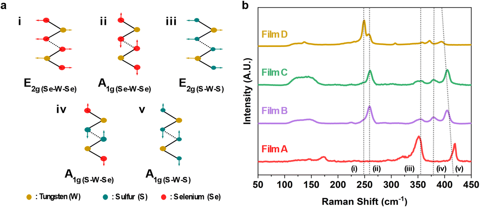 | ||
| Fig. 4 (a) A visual depiction of E2g and A1g vibrational modes for all possible binding configurations found within the binary and ternary films. (b) Raman spectral scan presented over a range of 50–450 cm−1, of the as-deposited WS2xSe2−2x films. | ||
Interestingly, the two ternaries (B and C from precursors (2) and (3)) also give rise to an additional peak located at ca. 380 cm−1. This is believed to be related to the out-of-plane vibration of both S and Se coordinated to a central W atom and will be hereon referred to as the (iv) A1g(S–W–Se) mode.54 The presence of this peak, along with the significant suppression of the peaks associated with WS2 and WSe2, signify the successful deposition of ternary WS2xSe2−2x. The broad feature located at ca. 150 cm−1 is reported to be a superposition of two second-order modes, namely the E2g(S–W–S)–LA(S–W–S) and the A1g(Se–W–Se)–LA(Se–W–Se).54 The significant enhancement of this peak in the ternary films further supports the presence of both S and Se within the film. A redshift was observed in the (v) A1g(S–W–S) mode with increased Se content within the film. This behaviour has been previously reported in WS2xSe2−2x alloys.54
The composition of the as-deposited TMDC films was investigated via X-ray photoelectron spectroscopy (XPS). Presented in Fig. S15† are the survey scans for all four as-deposited films. The films are free of impurities (e.g. C, Cl) which speaks to their high quality. From the survey scan, the spectrum shows peaks consistent with both binary and ternary WS2 and WSe2 films with the related orbitals labelled.14,57Fig. 5a–c presents the elemental scans of the W 4f, S 2p and Se 3d orbitals for the four films. It is worth noting that due to the overlap of atomic orbitals of the Se 3p and S 2p sub-shells, deconvolution of the S and Se contributions is required for the alloyed films.
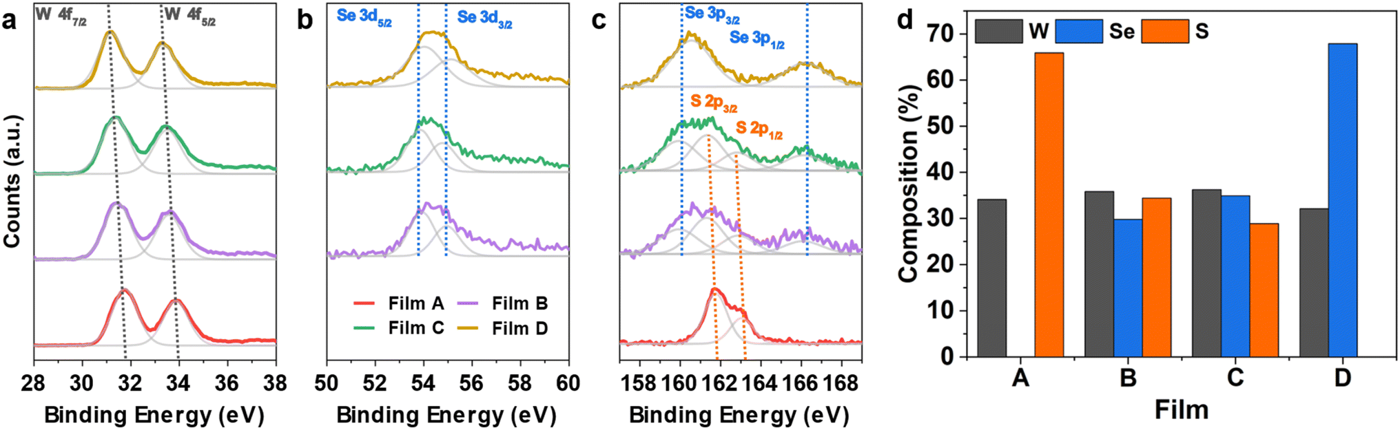 | ||
| Fig. 5 Elemental XPS scans of (a) W 4f, (b) Se 3d and (c) S 2p for all as-deposited WS2xSe2−2x films deposited from precursors (1–4). (d) Composition of all the as-deposited films deposited from precursors (1–4). | ||
In the W 4f scan (Fig. 5a) a single doublet formation is observed in all four films, which arises from spin–orbit coupling (W 4f7/2 and W 4f5/2). The position of the doublet indicates the W4+ oxidation state corresponding to the presence of tungsten chalcogenide bonds within the film.57,58 The absence of a W6+ oxidation state is characteristic of W-based TDMCs.57,59 The substitution of sulfur with selenium causes a small shift in the peaks related to W 4f and the S 2p orbitals to lower binding energies. This is indicated by the grey projection lines shown in Fig. 5a and agrees with previously reported values for the WS2 and WSe2 systems.60
Similarly, from the elemental scan of the Se 3d orbital (see Fig. 5b), two significant peaks were observed for films B to D, notably the Se 3d5/2 and Se 3d3/2 positioned at ca. 54 eV and ca. 54.8 eV respectively. These peaks are related to the Se2− oxidation state indicating Se bonded to W.61 The elemental scan of S 2p peaks on film A presents a doublet located at 161.5 eV and 162.7 eV, respectively, which correspond to 2p3/2 and 2p1/2 states in WS2,62 as shown in Fig. 5c. In terms of films B and C, XPS scans reveal the presence of both S and Se in the film through the existence of two doublets in the range 158 to 170 eV (Fig. 5c). This suggests that both precursors have successfully produced ternary tungsten chalcogenide films.
For accurate determination of composition, the peak separations were fixed for both the S and the Se doublets, with peak separations of 1.2 and 6.1 eV respectively, agreeing well with the literature.62 The doublet related to S 2p orbital is located at 161.2 and 162.4 eV, corresponding to the spin up (S 2p3/2) and spin down (S 2p1/2) states.62 The remaining area is associated with the Se 3p orbital which is situated at 160 and 166.1 eV, relating to the spin-up (Se 3p3/2) and spin-down (Se 3p1/2) states. The derived compositions of the two ternary films are shown in Fig. 5d, together with the two binaries. With films from (1) and (4) being stoichiometric WS2 and WSe2, respectively, precursors (2) and (3) each produced ternary films with 33% of W in both films. The stable W content suggests the successful deposition of ternary WS2xSe2−2x and also indicates both S and Se bound to a central W atom.62 Interestingly, precursor (3) produces a ternary film with a slightly lower sulfur concentration (x = 0.40) than that of the film from (2) (x = 0.48). We believe the slight difference in the composition originates from the different W–S/Se bonding present in precursors (2) and (3). While former has a WS double bond and a weaker W ← Se coordinate bond involving the neutral selenoether (SenBu2), on the other hand the latter features a WSe double bond and a W ← S coordinate bond (shown in Scheme 2). We believe that the chalcogenide bound to the W with a double bond in the precursor is more strongly bound and hence is dominant in the final film composition, which leads to the slightly higher S composition in film B and higher Se composition in film C. It is worth mentioning that it is possible to further control the composition by combination of the various single source precursors developed in this work with different ratios. This is enabled by the analogous nature of our 4 precursors and their compatible deposition temperatures.
 | ||
| Scheme 2 A molecular representation of precursors (1–4). | ||
3.2 Electrical characterisation
The electrical properties of the WS2xSe2−2x films deposited in this work were investigated. Fig. 6a presents the temperature-dependent electrical conductivity of the four films. Very interestingly, all films have relatively high electrical conductivities over 0.8 S cm−1 across the temperature range of 150 to 450 K. It is known that TMDCs can adopt two crystal structures, a metallic 1T phase and a semiconducting 2H phase, with the 1T phase being more favoured due to the larger electrical conductivity. However, issues regarding 1T phase stability have restricted the progress of this phase as it commonly reverts to the more stable 2H phase.63 In this work, despite the films all being found to be in the 2H coordination (illustrated by the XRD and the Raman spectra), all films yielded a strikingly high electrical conductivity when compared to literature.41,64–66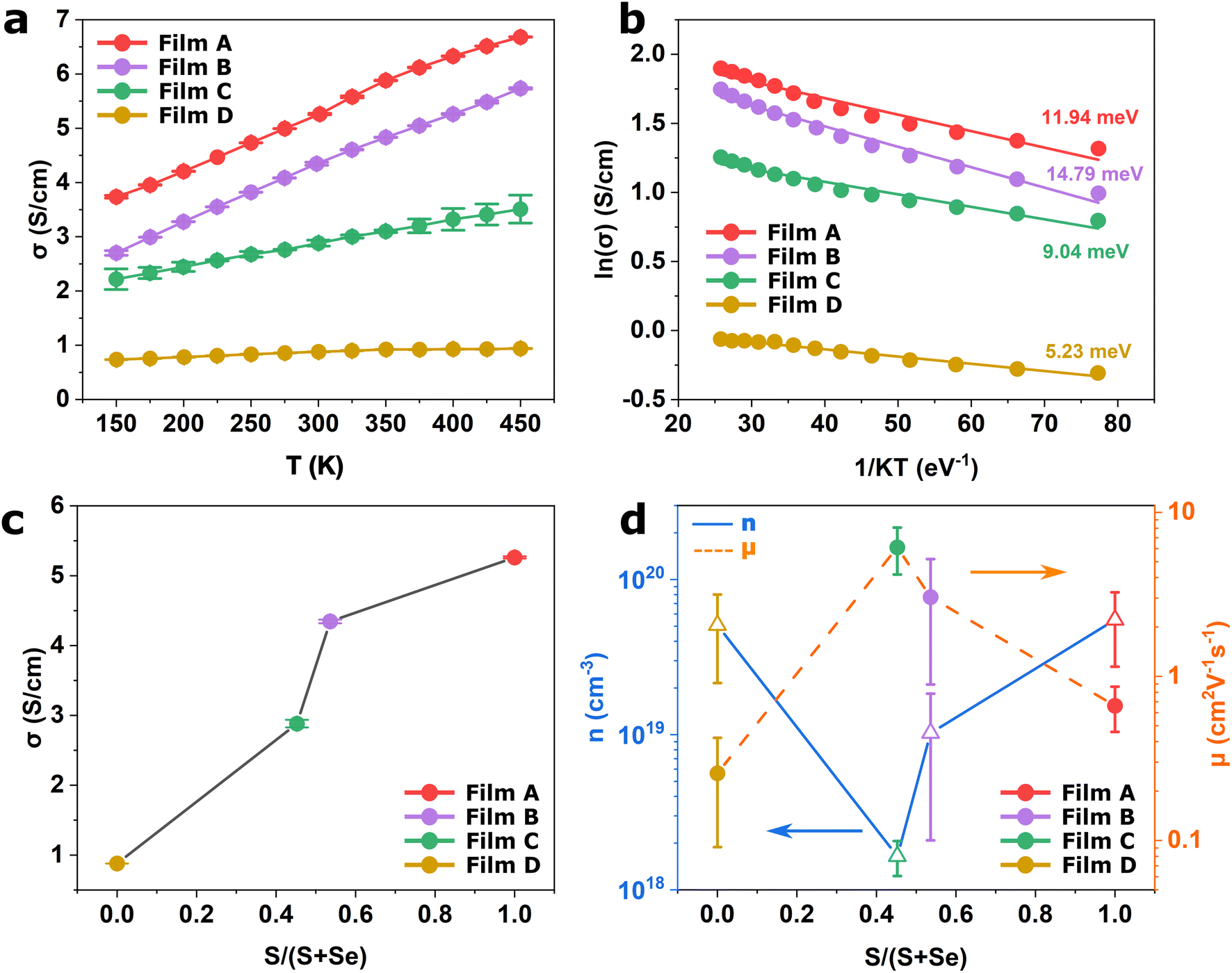 | ||
| Fig. 6 (a) Temperature-dependent electrical conductivity, (b) Arrhenius plot for WS2xSe2−2x films deposited from precursors (1–4). (c) Electrical conductivity and (d) Hall measurements against the chalcogenide content of the films. | ||
The 2H coordination would also suggest that the films will display semiconducting behaviour which is intrinsically temperature dependent due to the promotion of charge carriers to the conduction band upon absorption of thermal energy. For thermally activated conduction in semiconducting materials, the electrical conductivity (σ) can be expressed by the relation shown in eqn (1).67
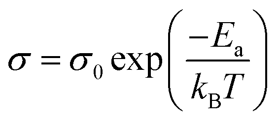 | (1) |
To shed more light on this behaviour, room temperature Hall measurements were conducted to explore the mechanism that governs the high electrical conductivity. Displayed in Fig. 6d is the majority carrier concentration (blue) and the carrier mobility (orange) as a function of the sulfur content in the film. It can be observed that all four films feature high carrier concentrations in the order of 1018 to 1020 cm−3. These are significantly larger than those typically reported for TMDCs41,43 and contribute to the high conductivities measured for the films. Such high carrier concentration is likely due to the formation of vacancies at the chalcogenide site on the crystallite surface. These vacancies act as self-dopants that enhance the carrier concentration of the film.68 On the other hand, the vacancies also act as scattering centres, which hinder carrier mobility,69 resulting in lower mobility compared with reports in literature.70,71 It is also likely that the platelet-like structures encompassed within the films also hinder carrier mobility through grain boundary scattering.72 It is worth mentioning that all four films demonstrate p-type conductivity. This is unsurprising for the WSe2 films which generally favours p-type conduction and have been integrated into p-type field effect transistors.73,74 However, WS2 films have been reported to display ambipolar behaviour in which concentrations of electrons and holes are of similar magnitudes.75 The absence of an anion (i.e. S vacancy), has been suggested to act as electron trap, with electrons aggregating around the anionic site.68,75 This would suppress the n-type conduction channel leading to the p-type behaviour being exhibited by the film. Interestingly, the two binaries show higher carrier concentrations than the ternaries. This implies that the binary films have a higher tendency to form surface vacancies compared to their alloyed counterparts.
To verify whether the vacancies drive the semi-metallic behaviour displayed in the as-deposited films, the two binary WS2 and WSe2 films were annealed in sulfur and selenium atmospheres, respectively, at 500 °C for 2 hours with the aim to suppress the vacancies formed at the chalcogenide site. Fig. 7 presents the effects on (a) carrier concentration and (b) carrier mobility for the as-deposited and post-annealed binary films. The annealed WS2 film was observed to have a near two orders of magnitude drop in carrier concentration from 5.50 × 1019 cm−3 to 5.62 × 1017 cm−3, along with an enhancement of carrier mobility (from 0.66 cm2 V−1 s−1 to 14.99 cm2 V−1 s−1). Similarly, annealing the WSe2 film in a selenium atmosphere also resulted in a significant drop in carrier concentration from 5.08 × 1019 cm−3 to 4.68 × 1018 cm−3 with a concurrent increase of carrier mobility from 0.26 cm2 V−1 s−1 to 4.39 cm2 V−1 s−1. Both cases strongly suggest that the suppression of chalcogen (i.e. sulfur and selenium) vacancies within the film upon annealing can induce significant changes in the self-doping level of our tungsten TMDCs. This offers an avenue for tuning the electrical performance of the TMDC films with an annealing process which can be beneficial for enhancing the performance of field effect transistors (FETs), photodiodes and optoelectronic devices.57,76,77
 | ||
| Fig. 7 (a) Carrier concentration and (b) carrier mobility of the as-deposited binary films, WS2 (red) and WSe2 (orange). Compared with the films annealed at 500 °C in the respective chalcogenide atmospheres. | ||
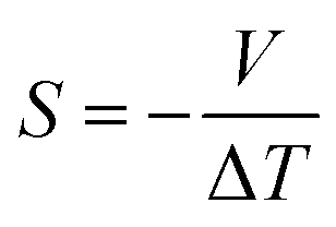
The phenomenon of thermoelectric power generation is based on the Seebeck effect, which can be understood by the relation shown in eqn (2).78
 | (2) |
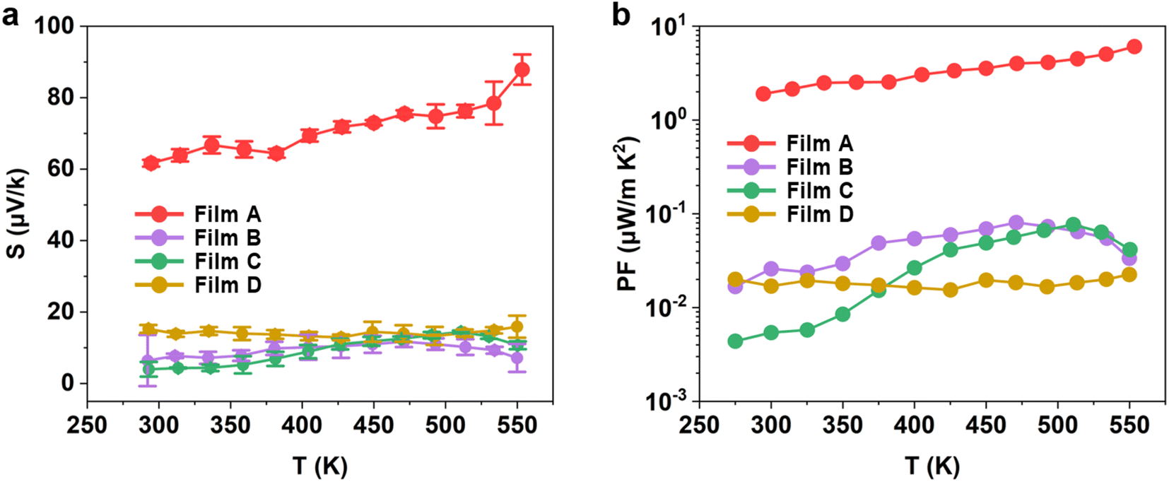 | ||
| Fig. 8 Temperature-dependent (a) Seebeck, and (b) power factor measurements for the WS2xSe2−2x films deposited from precursors (1–4). | ||
A useful parameter that is used to quantify and optimise the electrical-dependent properties of a thermoelectric material is the power factor, with the relation shown in eqn (3).
| PF = σS2 | (3) |
The improved Seebeck coefficient and the intrinsically high electrical conductivity of film A led to a peak power factor of 6 μW m−1 K−2 being achieved for the as-deposited WS2 film at 553 K, as shown in Fig. 8b. The performance of the as-deposited WS2xSe2−2x films created by such a simple and low-cost method is very encouraging. The enhanced electrical performance, as well as the ability to tune the performance, offer potential advantages regarding integration for a range of electrical and optical devices, as well as the potential fabrication of superlattice structures with alternating use of SSPs (1–4).29,81
4. Conclusions
In conclusion, this work reports the successful synthesis of a family of four distinct, but chemically quite analogous single source precursors, [WECl4(EnBu2)] (E = S, Se) suitable for the chemical vapour deposition of either binary or ternary WS2xSe2−2x thin films with good substrate coverage, high crystallinity and excellent stoichiometry, as confirmed by XRD, XPS and Raman measurements, along with significant evidence of the formation of W bound to both chalcogenides present in the alloyed films (S and Se). Hall measurements reveal that all the WS2xSe2−2x films displayed p-type semi-metallic behaviour. The films yielded electrical conductivities ranging from 0.85 S cm−1 to 5 S cm−1 with the conductivity increasing with the S content of the film. This high conductivity can be ascribed to its high carrier concentration which is likely to originate from the formation of vacancies at the chalcogenide site. However, significant suppression of carrier mobility was noted, likely due to increased defect scattering. The level of vacancies can be modulated through an annealing process, which enables the potential for tuning the electrical performance via the deposition conditions.Thermoelectric characterisation revealed a power factor of 6 μW m−1 K−2 for the as-deposited WS2, which was driven by the significantly enhanced electrical conductivity and a thermopower of 88 μV K−1 at 553 K. The enhanced electrical performance of undoped WS2xSe2−2x films, along with the deposition of pristine p-type WS2 offers promising avenues for the thermoelectric development of these materials, with the potential for further enhancements being realised through greater control of crystal growth, via precise control of the deposition conditions. The capability of controlling the electrical properties of the WS2xSe2−2x thin film through the selection of single source precursor and a simple annealing process certainly points towards the use of CVD-grown TMDC films in a wide range of electronic, thermoelectric and optical (nano)devices.
Author contributions
The manuscript was written through contributions of all authors. All authors have given approval to the final version of the manuscript.Conflicts of interest
There are no conflicts to declare.Acknowledgements
This work is financially supported by EPSRC via EP/P025137/1 and EP/V062689/1. V. S. and D. R. also thank EPSRC for their PhD studentships (EP/R513325/1, EP/N50947/1). We also thank the EPSRC for equipment funding under EP/K00509X/1 and EP/K009877/1. All data supporting this study are openly available from the University of Southampton repository at https://doi.org/10.5258/SOTON/D2572.References
- A. Chaves, J. G. Azadani, H. Alsalman, D. R. da Costa, R. Frisenda, A. J. Chaves, S. H. Song, Y. D. Kim, D. He, J. Zhou, A. Castellanos-Gomez, F. M. Peeters, Z. Liu, C. L. Hinkle, S. H. Oh, P. D. Ye, S. J. Koester, Y. H. Lee, P. Avouris, X. Wang and T. Low, npj 2D Mater. Appl., 2020, 4, 29 CrossRef CAS.
- J. Fan and M. Sun, Chem. Rec., 2022, 22, 1–34 CrossRef PubMed.
- A. Eftekhari, J. Mater. Chem. A, 2017, 5, 18299–18325 RSC.
- Z. Zhang, P. Chen, X. Yang, Y. Liu, H. Ma, J. Li, B. Zhao, J. Luo, X. Duan and X. Duan, Natl. Sci. Rev., 2020, 7, 737–744 CrossRef CAS PubMed.
- J. Huang, X. Wang, J. Li, L. Cao, Z. Xu and H. Wei, J. Alloys Compd., 2016, 673, 60–66 CrossRef CAS.
- P. Zhou, G. Collins, Z. Hens, K. M. Ryan, H. Geaney and S. Singh, Nanoscale, 2020, 12, 22307–22316 RSC.
- D. K. Nandi, U. K. Sen, A. Dhara, S. Mitra and S. K. Sarkar, RSC Adv., 2016, 6, 38024–38032 RSC.
- B. Zheng, D. Li, C. Zhu, J. Lan, X. Sun, W. Zheng, H. Liu, X. Zhang, X. Zhu, Y. Feng, T. Xu, L. Sun, G. Xu, X. Wang, C. Ma and A. Pan, InfoMat, 2020, 2, 752–760 CrossRef CAS.
- H. S. Ra, M. H. Jeong, T. Yoon, S. Kim, Y. J. Song and J. S. Lee, Adv. Sci., 2020, 7, 2001475 CrossRef CAS PubMed.
- J. S. Ross, P. Klement, A. M. Jones, N. J. Ghimire, J. Yan, D. G. Mandrus, T. Taniguchi, K. Watanabe, K. Kitamura, W. Yao, D. H. Cobden and X. Xu, Nat. Nanotechnol., 2014, 9, 268–272 CrossRef CAS PubMed.
- J. Pu, H. Ou, T. Yamada, N. Wada, H. Naito, H. Ogura, T. Endo, Z. Liu, T. Irisawa, K. Yanagi, Y. Nakanishi, Y. Gao, M. Maruyama, S. Okada, K. Shinokita, K. Matsuda, Y. Miyata and T. Takenobu, Adv. Mater., 2022, 34, 2203250 CrossRef CAS PubMed.
- D. Xu, P. Xu, Y. Zhu, W. Peng, Y. Li, G. Zhang, F. Zhang, T. E. Mallouk and X. Fan, ACS Appl. Mater. Interfaces, 2018, 10, 2810–2818 CrossRef CAS PubMed.
- B. Adilbekova, Y. Lin, E. Yengel, H. Faber, G. Harrison, Y. Firdaus, A. El-Labban, D. H. Anjum, V. Tung and T. D. Anthopoulos, J. Mater. Chem. C, 2020, 8, 5259–5264 RSC.
- Y. Koçak, Y. Akaltun and E. Gür, J. Phys.: Conf. Ser., 2016, 707, 012028 CrossRef.
- F. Godel, V. Zatko, C. Carrétéro, A. Sander, M. Galbiati, A. Vecchiola, P. Brus, O. Bezencenet, B. Servet, M. B. Martin, B. Dlubak and P. Seneor, ACS Appl. Nano Mater., 2020, 3, 7908–7916 CrossRef CAS.
- B. Pielić, D. Novko, I. Š. Rakić, J. Cai, M. Petrović, R. Ohmann, N. Vujičić, M. Basletić, C. Busse and M. Kralj, ACS Appl. Mater. Interfaces, 2021, 13, 50552–50563 CrossRef PubMed.
- A. Thangaraja, S. M. Shinde, G. Kalita and M. Tanemura, Mater. Lett., 2015, 156, 156–160 CrossRef CAS.
- X. Di, F. Wang, J. Wei, B. Zhang, X. Lin and K. Zhang, in China Semiconductor Technology International Conference 2019, CSTIC 2019, Institute of Electrical and Electronics Engineers Inc., 2019, pp. 1–3 Search PubMed.
- J. R. Brent, N. Savjani and P. O'Brien, Prog. Mater. Sci., 2017, 89, 411–478 CrossRef CAS.
- Q. Ji, Y. Zheng, Y. Zhang and Z. Liu, Chem. Soc. Rev., 2015, 44, 2587–2602 RSC.
- N. D. Boscher, C. J. Carmalt and I. P. Parkin, Eur. J. Inorg. Chem., 2006, 2006, 1255–1259 CrossRef.
- S. L. Benjamin, Y. P. Chang, C. Gurnani, A. L. Hector, M. Huggon, W. Levason and G. Reid, Dalton Trans., 2014, 43, 16640–16648 RSC.
- S. L. Benjamin, C. H. de Groot, C. Gurnani, S. L. Hawken, A. L. Hector, R. Huang, M. Jura, W. Levason, E. Reid, G. Reid, S. P. Richards and G. B. G. Stenning, J. Mater. Chem. C, 2018, 6, 7734–7739 RSC.
- P. J. McKarns, T. S. Lewkebandara, G. P. A. Yap, L. M. Liable-Sands, A. L. Rheingold and C. H. Winter, Inorg. Chem., 1998, 37, 418–424 CrossRef CAS PubMed.
- H. Wang, H. Yuan, S. Sae Hong, Y. Li and Y. Cui, Chem. Soc. Rev., 2015, 44, 2664–2680 RSC.
- X. Duan, C. Wang, A. Pan, R. Yu and X. Duan, Chem. Soc. Rev., 2015, 44, 8859–8876 RSC.
- X. Zhang, Z. Y. Al Balushi, F. Zhang, T. H. Choudhury, S. M. Eichfeld, N. Alem, T. N. Jackson, J. A. Robinson and J. M. Redwing, J. Electron. Mater., 2016, 45, 6273–6279 CrossRef CAS.
- Y. Sheng, H. Tan, X. Wang and J. H. Warner, Chem. Mater., 2017, 29, 4904–4911 CrossRef CAS.
- Y. Shi, H. Li and L. J. Li, Chem. Soc. Rev., 2015, 44, 2744–2756 RSC.
- G. Malandrino, Angew. Chem., Int. Ed., 2009, 48, 7478–7479 CrossRef CAS.
- S. D. Reid, A. L. Hector, W. Levason, G. Reid, B. J. Waller and M. Webster, Dalton Trans., 2007, 42, 4769–4777 RSC.
- N. D. Boscher, C. J. Carmalt and I. P. Parkin, Chem. Vap. Deposition, 2006, 12, 54–58 CrossRef CAS.
- N. E. Richey, C. Haines, J. L. Tami and L. McElwee-White, Chem. Commun., 2017, 53, 7728–7731 RSC.
- A. A. Tedstone, E. A. Lewis, N. Savjani, X. L. Zhong, S. J. Haigh, P. O'Brien and D. J. Lewis, Chem. Mater., 2017, 29, 3858–3862 CrossRef CAS.
- R. Huang, S. L. Benjamin, C. Gurnani, Y. Wang, A. L. Hector, W. Levason, G. Reid and C. H. De Groot, Sci. Rep., 2016, 6, 27593 CrossRef CAS PubMed.
- D. E. Smith, V. K. Greenacre, A. L. Hector, R. Huang, W. Levason, G. Reid, F. Robinson and S. Thomas, Dalton Trans., 2020, 49, 2496–2504 RSC.
- Y. P. Chang, A. L. Hector, W. Levason and G. Reid, Dalton Trans., 2017, 46, 9824–9832 RSC.
- C. Gurnani, S. L. Hawken, A. L. Hector, R. Huang, M. Jura, W. Levason, J. Perkins, G. Reid and G. B. G. Stenning, Dalton Trans., 2018, 47, 2628–2637 RSC.
- Y. P. Chang, A. L. Hector, W. Levason, G. Reid and J. Whittam, Dalton Trans., 2018, 47, 2406–2414 RSC.
- V. K. Greenacre, A. L. Hector, R. Huang, W. Levason, V. Sethi and G. Reid, Dalton Trans., 2022, 51, 2400–2412 RSC.
- N. Kumari, M. Kalyan, S. K. Ghosh, A. R. Maity and R. Mukherjee, Mater. Res. Express, 2021, 8, 45902 CrossRef CAS.
- J. H. Kim, S. Yu, S. W. S. Y. Lee, S. W. S. Y. Lee, K. S. Kim, Y. A. Kim and C. M. Yang, Crystals, 2020, 10, 140 CrossRef CAS.
- P. Sumathi, J. Chandrasekaran, R. Marnadu, S. Muthukrishnan and S. Maruthamuthu, J. Mater. Sci.: Mater. Electron., 2018, 29, 16815–16823 CrossRef CAS.
- M. W. Iqbal, M. Z. Iqbal, M. F. Khan, M. A. Shehzad, Y. Seo, J. H. Park, C. Hwang and J. Eom, Sci. Rep., 2015, 5, 1–9 Search PubMed.
- A. Sebastian, R. Pendurthi, T. H. Choudhury, J. M. Redwing and S. Das, Nat. Commun., 2021, 12, 1–12 CrossRef PubMed.
- K. Wu, C. Guo, H. Wang, X. Zhang, J. Wang and J. Chen, Opt. Express, 2017, 25, 17639 CrossRef CAS PubMed.
- D. J. Gulliver, E. G. Hope, W. Levason, S. G. Murray, D. M. Potter and G. L. Marshall, J. Chem. Soc., Perkin Trans. 2, 1984, 3, 429–434 RSC.
- S. Graulis, D. Chateigner, R. T. Downs, A. F. T. Yokochi, M. Quirós, L. Lutterotti, E. Manakova, J. Butkus, P. Moeck and A. Le Bail, J. Appl. Crystallogr., 2009, 42, 726–729 CrossRef PubMed.
- G. Bergerhoff, Inorganic Crystal Structure Database (ICSD), FIZ Karlsruhe, https://www.fiz-karlsruhe.de/en/produkte-und-dienstleistungen/inorganic-crystal-structure-database-icsd, accessed 3 June 2021 Search PubMed.
- W. J. Schutte, J. L. De Boer and F. Jellinek, J. Solid State Chem., 1987, 70, 207–209 CrossRef CAS.
- D. Zhang, T. Liu, J. Cheng, Q. Cao, G. Zheng, S. Liang, H. Wang and M. S. Cao, Nano-Micro Lett., 2019, 11, 1–15 CrossRef CAS PubMed.
- C. Lan, C. Li, J. C. Ho and Y. Liu, Adv. Electron. Mater., 2021, 7, 2000688 CrossRef CAS.
- X. Zhang, X. F. Qiao, W. Shi, J. Bin Wu, D. S. Jiang and P. H. Tan, Chem. Soc. Rev., 2015, 44, 2757–2785 RSC.
- X. Duan, C. Wang, Z. Fan, G. Hao, L. Kou, U. Halim, H. Li, X. Wu, Y. Wang, J. Jiang, A. Pan, Y. Huang, R. Yu and X. Duan, Nano Lett., 2016, 16, 264–269 CrossRef CAS PubMed.
- H. Zobeiri, S. Xu, Y. Yue, Q. Zhang, Y. Xie and X. Wang, Nanoscale, 2020, 12, 6064–6078 RSC.
- A. Berkdemir, H. R. Gutiérrez, A. R. Botello-Méndez, N. Perea-López, A. L. Elías, C. I. Chia, B. Wang, V. H. Crespi, F. López-Urías, J. C. Charlier, H. Terrones and M. Terrones, Sci. Rep., 2013, 3, 1–8 Search PubMed.
- Y. Fu, M. Long, A. Gao, Y. Wang, C. Pan, X. Liu, J. Zeng, K. Xu, L. Zhang, E. Liu, W. Hu, X. Wang and F. Miao, Appl. Phys. Lett., 2017, 111, 043502 CrossRef.
- F. Bozheyev, K. Harbauer and K. Ellmer, Sci. Rep., 2017, 7, 1–11 CrossRef CAS PubMed.
- Y. J. Noori, S. Thomas, S. Ramadan, V. K. Greenacre, N. M. Abdelazim, Y. Han, J. Zhang, R. Beanland, A. L. Hector, N. Klein, G. Reid, P. N. Bartlett and C. H. De Groot, 2D Mater., 2022, 9, 015025 CrossRef CAS.
- M. L. Zou, J. D. Chen, L. F. Xiao, H. Zhu, T. T. Yang, M. Zhang and M. L. Du, J. Mater. Chem. A, 2015, 3, 18090–18097 RSC.
- J. Guo, Y. Shi, X. Bai, X. Wang and T. Ma, J. Mater. Chem. A, 2015, 3, 24397–24404 RSC.
- R. Li, Y. Cheng and W. Huang, Small, 2018, 14, 1802091 CrossRef PubMed.
- M. S. Sokolikova, P. C. Sherrell, P. Palczynski, V. L. Bemmer and C. Mattevi, Nat. Commun., 2019, 10, 1–8 CrossRef PubMed.
- Z. Huang, T. Wu, S. Kong, Q. L. Meng, W. Zhuang, P. Jiang and X. Bao, J. Mater. Chem. A, 2016, 4, 10159–10165 RSC.
- H. Kawai, M. Sugahara, R. Okada, Y. Maniwa, Y. Yomogida and K. Yanagi, Appl. Phys. Express, 2017, 10, 15001 CrossRef.
- W. Y. Kim, H. J. Kim, T. Hallam, N. McEvoy, R. Gatensby, H. C. Nerl, K. O'Neill, R. Siris, G. T. Kim and G. S. Duesberg, Adv. Mater. Interfaces, 2018, 5, 1701161 CrossRef.
- R. Kumar and N. Khare, Thin Solid Films, 2008, 516, 1302–1307 CrossRef CAS.
- J. Yang, F. Bussolotti, H. Kawai and K. E. J. Goh, Phys. Status Solidi RRL, 2020, 14, 2000248 CrossRef CAS.
- A. N. Enyashin, M. Bar-Sadan, L. Houben and G. Seifert, J. Phys. Chem. C, 2013, 117, 10842–10848 CrossRef CAS.
- N. R. Pradhan, D. Rhodes, S. Memaran, J. M. Poumirol, D. Smirnov, S. Talapatra, S. Feng, N. Perea-Lopez, A. L. Elias, M. Terrones, P. M. Ajayan and L. Balicas, Sci. Rep., 2015, 5, 1–8 Search PubMed.
- L. Yang, K. Majumdar, H. Liu, Y. Du, H. Wu, M. Hatzistergos, P. Y. Hung, R. Tieckelmann, W. Tsai, C. Hobbs and P. D. Ye, Nano Lett., 2014, 14, 6275–6280 CrossRef CAS PubMed.
- F. Lan, R. Yang, K. Sun, Z. Wang, Y. Zhang, Y. Wang and H. Cheng, Vacuum, 2022, 201, 111091 CrossRef CAS.
- D. Kim, H. Du, T. Kim, S. Shin, S. Kim, M. Song, C. Lee, J. Lee, H. Cheong, D. H. Seo and S. Seo, AIP Adv., 2016, 6, 105307 CrossRef.
- H. Zhou, C. Wang, J. C. Shaw, R. Cheng, Y. Chen, X. Huang, Y. Liu, N. O. Weiss, Z. Lin, Y. Huang and X. Duan, Nano Lett., 2015, 15, 709–713 CrossRef CAS PubMed.
- G. Lee, S. Oh, J. Kim and J. Kim, ACS Appl. Mater. Interfaces, 2020, 12, 23127–23133 CrossRef CAS PubMed.
- T. H. Tsai, Z. Y. Liang, Y. C. Lin, C. C. Wang, K. I. Lin, K. Suenaga and P. W. Chiu, ACS Nano, 2020, 14, 4559–4566 CrossRef CAS PubMed.
- H. C. Kim, H. Kim, J. U. Lee, H. B. Lee, D. H. Choi, J. H. Lee, W. H. Lee, S. H. Jhang, B. H. Park, H. Cheong, S. W. Lee and H. J. Chung, ACS Nano, 2015, 9, 6854–6860 CrossRef CAS PubMed.
- T. J. Seebeck, Ann. Phys, 1826, 82, 253–286 CrossRef.
- P. Scherrer, Nachrichten von der Gesellschaft der Wissenschaften zu Göttingen, Mathematisch-Physikalische Klasse, 1918, 1918, 98–100 Search PubMed.
- Y. W. Gao, Y. Z. He and L. L. Zhu, Chin. Sci. Bull., 2010, 55, 16–21 CrossRef.
- Y. Hu, T. Yang, D. Li, G. Ding, C. Dun, D. Wu and X. Wang, ACS Omega, 2021, 6, 7879–7886 CrossRef CAS PubMed.
Footnote |
| † Electronic supplementary information (ESI) available. See DOI: https://doi.org/10.1039/d3ta00466j |
| This journal is © The Royal Society of Chemistry 2023 |