
CZTSSe solar cells: insights into interface engineering
Yimeng
Li
ab,
Hao
Wei
ab,
Changcheng
Cui
a,
Xiao
Wang
ac,
Zhipeng
Shao
 *ac,
Shuping
Pang
*ac and
Guanglei
Cui
*ac
*ac,
Shuping
Pang
*ac and
Guanglei
Cui
*ac
aQingdao Industrial Energy Storage Research Institute, Qingdao Institute of Bioenergy and Bioprocess Technology, Chinese Academy of Sciences, 266101 Qingdao, P. R. China. E-mail: shaozp@qibebt.ac.cn; pangsp@qibebt.ac.cn; cuigl@qibebt.ac.cn
bCenter of Materials Science and Optoelectronics Engineering, University of Chinese Academy of Sciences, 100049 Beijing, P. R. China
cShandong Energy Institute, 266101 Qingdao, P. R. China
First published on 22nd February 2023
Abstract
Cu2ZnSn(S,Se)4 (CZTSSe) photovoltaic (PV) technology has attracted much attention due to its cost efficiency, non-toxic nature, and use of earth-abundant elements. However, the current world record power conversion efficiency (PCE) of CZTSSe solar cells is 13.0%, lagging far behind the 23.4% of its predecessor Cu(In,Ga)Se2 (CIGS). The open-circuit voltage (VOC) deficit is always the key factor for the unsatisfactory efficiency of CZTSSe solar cells and is mainly related to the mismatch of the energy-band structure and deep-level defects at the interfaces. In this review, the current problems at the interfaces are discussed and recent works on interface engineering are summarized. Finally, we present our views on the challenges and prospects in this field.
1. Introduction
From the global market perspective, crystalline silicon solar cells will remain the mainstream photovoltaic market in the short term. Still, the transition toward thin-film solar cells and other new types of solar cells with low cost and environment friendliness has become an inevitable trend.1–5 Compared with crystal silicon solar cells, thin-film solar cells have greater scope for cost reduction and can be embedded in building-attached photovoltaic (BAPV) and building-integrated photovoltaic (BIPV) applications.6–8 Chalcogenide CdTe and CIGS solar cells have demonstrated efficiencies of over 20% and long-term stability and have been commercially available for decades.9,10 From a sustainability perspective, CdTe and CIGS solar cells can hardly dominate the PV market, mainly due to the scarcity of Te, In, and Ga.11–14 High abundance, low-priced, and eco-friendly semiconductors are thus needed for high-performance thin-film solar cells.15–17 By replacing In and Ga with inexpensive, abundant, and non-toxic Zn and Sn, CZTSSe solar cells are currently considered one of the best choices.18–20CZTSSe films have advantages in the following aspects:21–25 element abundant reserves, low price, and environmental friendliness, which give the future commercialized CZTSSe solar cells a significant advantage in manufacturing costs and sustainable development potential.5,26 Furthermore, CZTSSe is a stable direct bandgap p-type semiconductor material with a bandgap that varies in the range of 1.0 to 1.5 eV depending on the S/Se ratio, which matches the standard solar spectrum very well.15,27 In addition, CZTSSe has an absorption coefficient of up to the order of 104 cm−1, while only 1–2 microns are needed for full light absorption.27,28 The excellent photovoltaic property of CZTSSe allows it produce high-efficiency multi-junction thin-film solar cells combined with GaAs or perovskite solar cells.27,29,30
However, the current record efficiency of CZTSSe solar cells is 13.0% (VOC = 529.4 mV, short-circuit current density (JSC) = 33.6 mA cm−2, fill factor (FF) = 72.9%), which is far from the 23.4% of the high-performance CIGS solar cells (VOC = 734.0 mV, JSC = 39.6 mA cm−2, FF = 80.4%). The VOC, JSC, and FF of the best-performing CZTSSe solar cell are only 59.7%, 80.2%, and 81.9% of the theoretical values, which are much lower than the corresponding values for CIGS.27,31,32 The difference between CZTSSe and CIGS comes mainly from the VOC deficit caused by the severe charge recombination in CZTSSe devices.33–36 As a five-membered material, CZTSSe has more self-interstitial vacancies and defect clusters than binary and ternary semiconductor materials. Due to the similar chemical properties of Cu (1.32 Å) and Zn (1.22 Å) and their similar ionic radii, the absorbing materials are prone to defects with a low formation energy. Calculations based on density functional theory (DFT) showed the presence of vacancies in the material: VZn, VCu, VSn, antisite defects: CuSn, CuZn, SnZn, defect clusters: VCu + ZnCu, VZn + SnZn, ZnSn + 2ZnCu, etc. The simulations showed that VCu and CuZn defects have a small formation energy, which is the underlying reason for the more significant concentration of CuZn defects in the p-type CZTSSe semiconductor.37,38 Deep energy level defect states in the bulk phase lead to severe band tail states in the material, which act as recombination centers, leading to non-radiative recombination that reduces the solar cell carrier lifetime. Compared to CIGS solar cells, CZTSSe solar cells have poor carrier-transport capabilities due to interfacial recombination.39 It was also found that the individual interface recombination in CZTSSe solar cells is influenced by several factors, such as energy level matching, interface defects, and the carrier concentration of the absorber layer and other contact materials.33,39,40 In conventional CZTSSe solar cells, there are two dominant interfaces from the front electrode to the Mo back electrode: (1) the CZTSSe/CdS interface, known as the front interface and (2) the Mo/CZTSSe interface, known as the back interface.33 The interface determines the carrier separation, collection, and recombination. Interface engineering is an effective way of suppressing interfacial recombination and improving the VOC. It is essential to assess the relevant properties of the interface, the mechanisms of recombination at different interfaces, and the collection of charge carriers at the interface.6,11,23,33,41
This review provides insights into interface engineering and the strategies employed at the interfaces, divided into three sections. The first section mainly presents the problems and solutions at the back interface, and this section contains two branches: the blocking layer and the sacrificial layer. In the second section, the problems at the front interface and the efforts made on these problems are described and analyzed in detail. This section includes the following points: the passivation layers, alternative buffer layers, and heterojunction annealing. Finally, we present our views on the challenges and prospects in this field and discuss proposals for further improvements in interface engineering for CZTSSe solar cells.
2. Interface engineering
2.1 Back interface
 | ||
| Fig. 1 (a) Schematic diagram of Se diffusion through CZTSSe/MoSe2/Mo during high-temperature annealing.48 Reproduced with permission from ref. 48. (b) Equilibrium S vapor pressure vs. sulfurization temperature for the reactions and equilibrium Se vapor pressure vs. selenization temperature for the reactions.49 Reproduced with permission from ref. 49. (c) Pinholes at the back interface of the CZTSSe solar cell.50 Reproduced with permission from ref. 50. | ||
Detailed thermodynamic investigations were reported by Scragg et al.,51 who indicated that the Mo/CZTSSe interface exhibits lower chemical stability than Mo/CIGS. The net free energy change (ΔG) associated with the absorber layer measured at 550 °C showed that ΔG is positive for CIGS while negative for CZTS and CZTSe at −150 kJ mol−1 and −100 kJ mol−1, respectively, indicating the instability nature of CZTSSe during the thermal annealing. The following side reactions occur at the back interface during the selenization process.
| 2Cu2ZnSnS(e)4 + Mo 2Cu2S(e) + 2ZnS(e) + 2SnS(e) + MoS(e)2 |
| Se(g) + Mo MoS(e)2 |
The side reactions form the secondary phases and bring in defects at the CZTSSe/Mo interface. While every coin has two sides. A thinner MoSe2 interfacial layer not only facilitates the formation of ohmic contacts at the back interface but also allows for increased adhesion between Mo and CZTSSe layers.23,52 Cozza et al.53 demonstrated through theoretical simulations and experimental results that an appropriately thick MoSe2 interfacial layer is a prerequisite for the preparation of highly efficient devices. However, as mentioned above, due to the back interface instability during selenization and excessive amounts of selenium, excessively thick MoSe2 interfacial layers are often generated, which can be hundreds or thousands of nanometers thick, resulting in increased series resistance (RS) and reduced FF values of the cells.54 The thick MoSe2 layer can also act as a carrier scattering center, exacerbating back-interface recombination,55 even when the absorber layer has excellent crystalline quality.56–58
The side reactions also lead to pinholes.44,59 The continuous removal of gaseous byproducts [SnS(e) and ZnS(e)] from the annealed environment during sulfurization or selenization creates pinholes at the interface.34,51 Similarly, pinholes are also formed due to the Kirkendall effect between elemental copper and its sulfide or selenide derivatives [i.e., CuS(e)] during the high-temperature thermal annealing process.23 The Cu element exhibits a higher diffusivity than S, thus forming pinholes, and these pinholes can rupture again en masse to form larger pinholes at the Mo/absorber interface.18
Optimizing the properties of the back interface is critical to improving the device performance. Researchers have introduced numerous interfacial layer materials at the back interface, and the current state of research in this area is shown in Table 1. Here we classified the interfacial layers into two categories depending on their properties: the blocking layer, where the interfacial layer material does not participate in the reaction in the selenization process;42,44,58,60–66 and the sacrificial layer, which is introduced to take part in the reaction during selenization.43,46
| Categories | Absorber | Intermediate layer | V OC (mV) | J SC (mA cm−2) | FF (%) | PCE (%) | References |
|---|---|---|---|---|---|---|---|
| Blocking layer | CZTS | Al2O3 | 657 | 19.8 | 65.9 | 8.6 | 67 |
| w. o. Al2O3 | 632 | 19.0 | 61.1 | 7.3 | |||
| CZTSe | MoO2 | 393 | 32.6 | 63.6 | 8.2 | 68 | |
| w. o. MoO2 | 385 | 31.8 | 59.6 | 7.3 | |||
| CZTSSe | MoO3 | 465 | 37.9 | 64.0 | 11.3 | 69 | |
| w. o. MoO3 | 399 | — | — | 8.4 | |||
| CZTS | AZO | 681 | 19.5 | 63.4 | 8.4 | 58 | |
| w. o. AZO | 665 | 18.8 | 57.1 | 7.1 | |||
| CZTSSe | C | 514 | 38.2 | 68.8 | 13.5 | 63 | |
| CZTSe | TiN | 385 | 42.6 | 54.2 | 8.9 | 70 | |
| w. o. TiN | 264 | 25.4 | 44.0 | 3.0 | |||
| Sacrificial layer | CZTSSe | VSe | 332 | 28.7 | 46.2 | 4.4 | 71 |
| w. o. VSe | 389 | 28.4 | 55.6 | 6.2 | |||
| CZTS | Na2S | 337 | 12.7 | 53.6 | 2.3 | 43 | |
| w. o. Na2S | 330 | 10.4 | 34.5 | 1.1 | |||
| CZTSSe | GeO2 | 547 | 70.0 | 34.3 | 13.1 | 46 | |
| w. o. GeO2 | 496 | 68.0 | 33.6 | 11.3 |
So far, there is currently no universal back-interface engineering solution to significantly improve the efficiency of CZTSSe solar cells. Further refining of the experimental design and exploring a more suitable back-interface interlayer to optimize CZTSSe thin-film solar cells are thus needed in the following research.
Al2O3 is a shining star among the many blocking layers due to its unique advantage. Liu et al. reported that by introducing an Al2O3 interlayer between Mo and CZTS, the interfacial reaction between CZTS and Mo is suppressed at the early stage of sulfuration, and that pinholes and phase segregation in the back-contact region can be well eliminated. The addition of the Al2O3 blocking layer increases the conversion efficiency of the ultrathin CZTS solar cell from 7.34% to 8.56%. Also, this back-interface contact was proved to be effective and reproducible in normal-thickness CZTS devices.67 The chemically inert conductor titanium nitride (TiN) effectively passivates the Mo/CZTS interface and can block the interfacial reaction between Mo and S in the annealing atmosphere, whereas Na transport from the substrate is unaffected, as shown in Fig. 2a. Unfortunately, the TiN/CZTS contacts generate a relatively high series resistance.44 Therefore, further research is needed to develop blocking layers with better properties. Recently, many researchers have concluded that MoO3 is an ideal blocking layer for the Mo/CZTSSe interface.69,72–74 Currently, the main methods for introducing MoO3 interfacial layers are: (i) high-temperature annealing, (ii) magnetron sputtering, (iii) thermal evaporation, and (iv) spin coating. In 2019, Yu et al. found that the multilayer crystalline behavior of CZTSSe was induced by the formation of a secondary phase at the back interface, which was a chemical reaction between Mo and CZTSSe. An in situ-grown MoO3 isolation layer was successfully introduced to block the reactions. They further found that, in addition to MoO3, other materials such as SiO2, TiN, and MoSe2, were also effective in eliminating multilayer crystallization, as shown in Fig. 2b.69 The insertion of a p-type contact MoO3 with a high work function between the CZTSSe and Mo electrodes not only blocked the occurrence of back-interface side reactions but also enabled the formation of an interfacial field, which accelerated carrier separation, as shown in Fig. 2c.74 Recently, Sun et al. used the porous MoO3 array structure as a post-interface contact and elaborated on the effect of the MoO3 microstructure on CZTSSe photovoltaic devices. This interpenetrating structure of the porous array not only helped to create a favorable interfacial field for effective carrier separation but also increased the interfacial contact area to extend the light propagation path through porous scattering and accelerated the aggregation of holes along the hole walls toward the Mo electrode, as shown in Fig. 2c.74
 | ||
| Fig. 2 (a) Schematic diagram of TiN action in the high-temperature annealing process.44 Reproduced with permission from ref. 44. (b) Diagram of grain growth without and with MoO3 blocking layer.69 Reproduced with permission from ref. 69. (c) The structure diagram of the CZTSSe solar cell, the band diagram of Mo/MoSe2/CZTSSe and Mo/MoO3/CZTSSe, and the boundary face transfer diagram of interpenetrating MoO3/CZTSSe arrays.74 Reproduced with permission from ref. 74. | ||
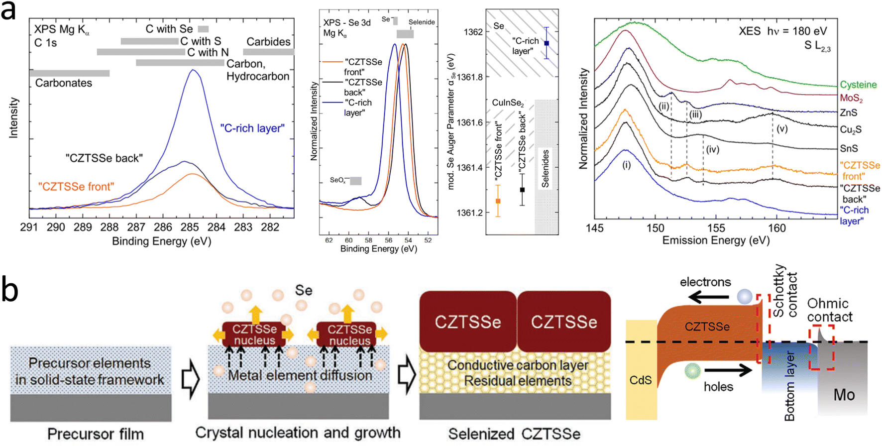
An emerging blocking layer has recently received much attention. The in situ interface layer is mainly the C-rich layer that remains from the selenization process.63–65 Mercaptoethanolic acid (TGA)-amino aqueous solutions are susceptible to a CZTSSe grain phase bias growth behavior during selenization driven by the presence of a conductive carbon framework layer and the thermodynamic properties of the non-homogeneous thin-film system. A C-rich layer can play an essential role in improving the electrical contact between CZTSSe and Mo, allowing the formation of an ohmic contact at the absorption layer/Mo interface, thus enhancing the PCE of CZTSSe solar cells.
In 2021, an aqueous solution of ammonium thioacetate (ATGL) was reported by D. Hauschild et al., and they obtained a ‘buried’ back-contact interface by cleavage in a liquid nitrogen environment.64 This work presented a detailed picture of the chemical structure of this carbon-rich layer at the back-contact, which consisted of carbon (74 ± 7%), selenium (19 ± 4%), and sulfur (7 ± 3%). The selenium in this layer was in the form of elemental inclusions. The sulfur content of this carbon-rich layer was twice as high as that of the absorber. Detailed analysis of the chemical environment indicated that residues of the aqueous ATGL solution were the source of sulfur in this carbon-rich layer. In addition, S–Mo bonds were found beneath the carbon-rich layer at the back-contact of Mo; the specific data are shown in Fig. 3a. In the same year, the existence of a conductive carbon framework layer was explained more clearly by Xu et al., and schematic diagrams of the TGA-ammonia method and the energy-band structure of the cell are shown in Fig. 3b.63 The interconnected mesoscopic carbon framework was mainly formed by large metal–organic clusters induced by the Sn-TGA coordination structure. The Sn had a six-coordinated design, and the deprotonated TGA had a double-coordinated end group.77–79 The carbon layers could buffer the elemental composition fluctuations of the top CZTSSe grains by accommodating residual metallic elements or secondary phases on the one hand and facilitated the charge transport of the cell by improving the mechanical and electrical contact between the CZTSSe and Mo electrodes on the other.
In earlier studies, researchers found that sodium–calcium glass as a base material for CZTSSe solar cells could significantly improve the performance.82–84 This was mainly due to the diffusion of Na into the absorber layer during high-temperature selenization to passivate the defects and enhance the absorber layer's crystal quality.85,86 Since then, sodium doping has been of interest to researchers.87–90 In 2018, Gu et al. found that the insertion of a Na2S self-consuming layer could effectively stabilize the CZTS/Mo interface. A schematic diagram of the CZTS solar cells is shown in Fig. 4a. This eliminates the side reaction between CZTS and Mo, thereby improving the crystallinity of the CZTS absorbing layer, enhancing carrier transport at the CZTS/Mo interface, and reducing the series resistance.43 In addition, the self-consumption property of the Na2S sacrificial layer also averts the holes-transport barrier. Recently, Wang et al. developed a convenient and effective method to simultaneously design CZTSSe absorbers with back interfaces and bulk defects by introducing a GeO2 layer on a Mo substrate, as shown in Fig. 4b.46 Based on the optimum GeO2 concentration, the CZTSSe device achieved a PCE of up to 13.14% with a VOC of 547 mV. Further studies have shown that when selenization occurs, bidirectional diffusion co-occurs in the upward CZTSSe absorber layer and downward in the MoSe2 layer. A portion of Ge diffuses into the absorber and combines with Se to form Ge–Se liquid fluxes, promoting nucleation and grain growth, resulting in flatter CZTSSe films with fewer pinholes. This can significantly reduce the defect density, band tail, and promote quasi Fermi-level splitting through the relatively higher hole concentration. At the same time, another part of Ge diffuses into the MoSe2 layer, increasing the work function of MoSe2, which may act as an electronic barrier at the back interface and inhibit the recombination of photogenerated carriers. As a result, the device achieved a VOC/VOCSQ of 63.1%, which is the lowest VOC loss of any Ge-doped CZTSSe solar cells reported.

2.2 Front interface
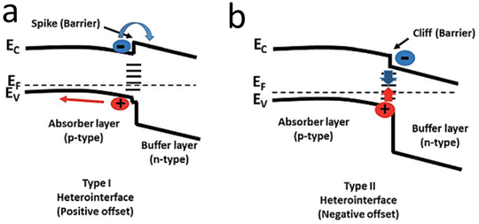 | ||
| Fig. 5 Types of heterojunction interface alignments for the absorber and buffer layers: (a) type I (spike), (b) type II (cliff).33 Reproduced with permission from ref. 33. | ||
In CZTSSe, the surface could not form the n-type due to the dissolution of Zn2+ on its surface by the ammonia (NH3·H2O) in the solution during the deposition of CdS to form Zn vacancies, and the occupation of Zn vacancies (not Cu vacancies) by Cd2+, resulting in lattice strain due to the significant difference in the radii of the Cd2+ and Zn2+ ions.15,27,32,95 It was found experimentally that the surface of CZTSSe was indeed a p-type (no type inversion),3 in agreement with the theoretical analysis. Since the maximum VOC under illumination (in the band conditions shown in Fig. 6) was equal to the band bending of the absorber layer in the dark, Fermi-level pinning caused by the surface CuZn defects (and hence no type inversion) led to a substantial deficit in VOC.95 This inability of the surface to achieve p–n inversion hindered the VOC. In contrast, type-reversal band bending was observed in the CIGS solar cells, which gave them a much higher VOC than the CZTSSe solar cells, as shown in Fig. 6c and d.95–97 Therefore, if the intention is to overcome the VOC deficit in CZTSSe solar cells, it is crucial to suppress the formation of CuZn defects and make the type conversion at the p–n junction interface possible.
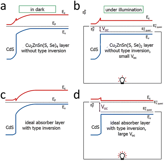 | ||
| Fig. 6 Band diagrams of solar cells in the dark (left) and under illumination (right). (a) CdS/CZTSSe solar cells without type inversion (Fermi level near the interface pinned to the middle of the band gap) and with a slight band bending in the absorber layer, and (b) CdS/CZTSSe solar cells with negligible VOC under flat band conditions. (c) Ideal absorber layer with type reversal (Fermi level near the interface close to the conduction band), considerable band bending, and (d) perfect absorber layer with significant VOC under in-band flat conditions.95 Reproduced with permission from ref. 95. | ||
Researchers have done much work on heterojunctions to solve energy-band-alignment mismatches and interfacial defects.24,39 The optimization of heterojunctions can be split into three main areas: introduction of ultrathin passivation layers,98–100 alternative buffer layers,101–105 and annealing of heterojunctions.32,40,106–109 An ultrathin passivation layer alters the local chemistry of the surface and reduces defect-assisted interfacial recombination.100 Alternative buffer layers can replace conventional CdS buffer layers with tunable band gaps to create a favorable band alignment.11,103 Furthermore, heat treatment after deposition of the CdS buffer layer can significantly improve the performance of the heterojunction due to the formation of interlayers and the compensation of defects by diffusion between the elements.32,108
Wu et al. reported that ALD-coated TiO2 films on CZTSSe photovoltaic devices could reduce interfacial recombination and improve device performance, as shown in Fig. 7a. After ALD deposition, the VOC of the device was increased from 397 mV to 433 mV.110 These results clearly illustrate the surface passivation effect of the ALD layer in CZTSSe devices and showed that adding an ALD passivation layer is a potential way to improve the VOC. Subsequently, Sun et al.111 used the successive ionic layer adsorption and reaction (SILAR) method to deposit an ultrathin SnO2 interlayer, which was introduced into the heterogeneous interface between a p-type CZTS absorber and an n-type CdS buffer for passivation of the interfacial defects in CZTSSe thin-film solar cells, and the specific details are shown in Fig. 7b. The VOC values of CZTS with and without the SnO2 interlayer were 657 mV and 638 mV, and the FF values were 62.8% and 52.4%, respectively. The mitigation of the VOC deficit and improvement in FF were believed to result from the combined effects of CZTS/CdS heterogeneous interfacial passivation, shunt blocking, and band alignment.
 | ||
| Fig. 7 (a) J–V curves of an ALD–TiO2-treated CZTSSe cell.110 Reproduced with permission from ref. 110. (b) Schematic band diagrams of the CZTS/SnO2/CdS heterojunctions and J–V curves.111 Reproduced with permission from ref. 111. (c) Schematic band gap fluctuation in the electronic structures of CZTS with and without Al2O3 treatment and mechanism illustration of the CZTS absorber surface modification when exposed to ALD–Al2O3 treatment.100 Reproduced with permission from ref. 100. (d) SEM top-view images of CZTSSe/CdS and CZTSSe/In2S3/CdS films and EDS mapping images, surface AFM images of bare CZTSSe films (0 min) and CZTSSe/In2S3 films for different In2S3 deposition times (3, 6, 9 min) and schematic representation of the other morphological evolution mechanisms according to the presence of In2S3 layers.112 Reproduced with permission from ref. 112. | ||
Many researchers later considered the conformal coating of Al2O3 grown on CZTSSe by ALD as an effective method to reduce interfacial recombination. Some also found that inserting a thin Al2O3 layer between CdS and TCO could also work as armor shield to prevent damage to CdS during TCO fabrication.98–100 Xiaojing Hao's group found that applying a complete ALD–Al2O3 cycle and trimethyl aluminum (TMA) exposure resulted in a significant increase in VOC and linked this to the properties of the CZTS interface. Both processes favored the formation of a thicker Cu-deficient nanolayer with higher concentrations of Na and O, forming a homogeneous passivation layer on the CZTS surface. The nanolayer reduced potential local fluctuations at the band edge, widened the electric band gap, and suppressed recombination at the heterojunction interface, thereby improving the VOC and device performance, as shown in Fig. 7c. The ability of the nanolayer to alter the atomic composition of the near-surface region makes it a universal approach for surface passivation.100
Recently, an In2S3 passivation layer was used with the CZTSSe/CdS interface to improve the front interface roughness and reduce interfacial recombination, and it was demonstrated that this method could effectively control the surface morphology and defect density of CZTSSe thin-film solar cells.112 The presence of the In2S3 layer led to an homogeneous growth of CdS without macroscopic CdS agglomeration (i.e., a reduced roughness of the full device), thereby improving the quality of the heterojunction (as shown in Fig. 7d). The In2S3 passivation layers contributed to the reduction of non-radiative recombination by reducing the deep energy level defects and increasing the minority carrier lifetimes. Similarly, the improved interfacial morphology and photovoltaic performance provided by the thin In2S3 passivation layers were very promising for both CZTSSe single solar cells and tandem solar cells, as the relatively rough surface and poor photovoltaic performance are currently the main obstacles to achieving efficient CZTSSe-based tandem solar cells.
| Buffer layer | Absorber | Deposition method | Thickness (nm) | V OC (mV) | J SC (mA cm−2) | FF (%) | PCE (%) | References |
|---|---|---|---|---|---|---|---|---|
| ZnSnO | CZTS | ALD | 10 | 720 | 20.5 | 63.5 | 9.3 | 13 |
| CZTS | ALD | 10 | 736 | 21.0 | 65.8 | 10.2 | 100 | |
| CZTS | ALD | 56 | 746 | 19.1 | 68.0 | 9.7 | 11 | |
| CZTS | RF sputtering | 50 | 721 | 14.0 | 51.4 | 5.2 | 115 | |
| CZTSSe | RF sputtering | ∼20 | 445 | 36.4 | 69.3 | 11.2 | 103 | |
| ZnCdS | CZTS | SILAR | 70 | 747 | 19.5 | 63.2 | 9.2 | 102 |
| CZTS | SILAR | 70 | 735 | 20.1 | 62.5 | 9.3 | 105 | |
| CZTS | CBD | 60 | 683 | 22.2 | 66.3 | 10.1 | 104 | |
| Zn(O,S) | CZTSSe | CBD | — | 346 | 34.8 | 47.8 | 5.8 | 121 |
| CZTSSe | ALD | 20 | 496 | 35.6 | 56.0 | 9.8 | 122 | |
| ZnS | CZTSSe | CBD | 30–50 | 596 | 15.4 | 49.1 | 4.5 | 123 |
| CZTSSe | CBD | 70 | 309 | 23.5 | 54.0 | 3.8 | 124 | |
| In2S3 | CZTS | CBD | 90 | 585 | 17.0 | 45.0 | 4.5 | 101 |
| CZTS | CBD | 60 | 738 | 17.6 | 55.5 | 7.2 | 125 |
Non-toxic, environmentally friendly wide-band-gap n-type semiconductors with suitable CBO are favorable for alternative buffer layers.126 Among the many alternative buffer layers, ZnSnO is a shining star due to its unique advantages. The band gap can be adjusted by adjusting the Zn/Sn ratio; the structure of the interfacial energy band is shown in Fig. 8a.103 The increased efficiency of ZnSnO is not only due to the excellent energy-band alignment but also to the formation of an ultrathin Zn(O,S) tunneling layer between CZTS/ZnSnO, which acts as an effective cavity barrier at the interface.13 Atomic layer deposition (ALD) is a widely adopted method for depositing ZnSnO buffers. The properties of the ZnSnO buffer layer can be tuned by adjusting the deposition temperature and the metal stoichiometry ratio, as shown in Fig. 8b.100,103 The structure of a CZTS solar cells device with a ZnSnO buffer layer is shown in Fig. 8c. Wang et al. introduced an additional In2S3 buffer layer to modify the properties of the Zn(O,S) and CZTSSe layers by a post-annealing treatment. The increased carrier concentration in the Zn(O,S) and CZTSSe layers facilitated carrier separation and increased the VOC. The results showed that the efficiency of CZTSSe solar cells was increased by 24% after the annealing and etching treatment. Simulation and experimental results showed that the significant band shift of the In2S3 layer and the defect energy level of the Zn(O,S) layer were the main characteristics limiting the FF and efficiency of these CZTSSe devices, as shown in Fig. 8d.121 The In2S3 material is an effective alternative to CdS buffer layers due to its non-toxic and suitable indirect band gap (Eg = 2.1 eV). The CZTS/In2S3 heterojunction with a positive CBO of 0.11 eV facilitated carrier separation and transport at the interface, as shown in Fig. 8e. However, the CBO of CZTSSe/In2S3 was more significant than 0.4 eV, which is not conducive to carrier transport, so it has been less studied as a buffer layer.101
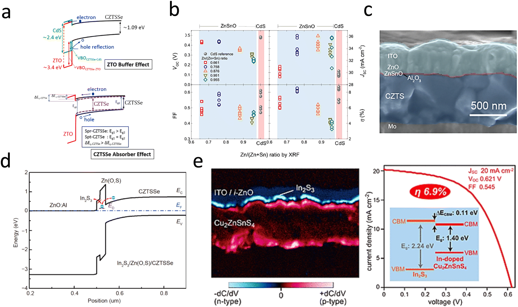 | ||
| Fig. 8 (a) Schematic diagram of the energy-band structure between CZTSSe and ZnSnO.103 Reproduced with permission from ref. 103. (b) CZTSSe/CdS and CZTSSe/ZnSnO device performance with different Sn, Zn ratios.120 Reproduced with permission from ref. 120. (c) SEM cross-sectional image of Cd-free CZTS solar cells with an Al2O3 passivation layer inserted between CZTS and ZnSnO.100 Reproduced with permission from ref. 100. (d) Schematic diagram of the band alignment of the In2S3/Zn(O,S)/CZTSSe interface for the device.121 Reproduced with permission from ref. 121. (e) Cross-sectional SCM images of solar cells based on In2S3/Cu2ZnSnS4 and J–V curves.101 Reproduced with permission from ref. 101. | ||
| Absorber | Annealing | Step | Atmosphere | V OC (mV) | J SC (mA cm−1) | FF (%) | PCE (%) | References | ||
|---|---|---|---|---|---|---|---|---|---|---|
| Temp. (°C) | Time (min) | Before | After | |||||||
| CZTSSe | 220 | 3 | After cell | Air | 358 | 27.9 | 32.9 | 3.7 | 3.3 | 107 |
| 270 | 3 | 424 | 31.7 | 59.7 | 4.4 | 8.0 | ||||
| 320 | 3 | 400 | 28.1 | 38.6 | 4.3 | 4.3 | ||||
| CZTS | 270 | 10 | After CdS | N2 | 731 | 21.7 | 69.3 | 7.8 | 11.0 | 108 |
| CZTSSe | 200 | 2 | After CdS | Vacuum | 522 | 33.3 | 71.5 | 10.9 | 12.4 | 109 |
| 200 | 20 | 513 | 35.1 | 72.5 | 10.9 | 13.0 | ||||
| CZTSSe | 90 | 60 | After CdS | N2 | 476 | 36.7 | 63.0 | 10.4 | 11.1 | 94 |
| 210 | 1 | 472 | 36.7 | 57.0 | 10.4 | 10.0 | ||||
| 90–210 | 60–1 | 487 | 37.0 | 67.0 | 10.4 | 12.1 | ||||
| CZTSSe | 250 | 5 | After CdS | N2 | 362 | 27.6 | 45.6 | 7.6 | 4.6 | 127 |
| 300 | 5 | 350 | 25.9 | 32.1 | 7.6 | 2.9 | ||||
| CZTSSe | 150 | 90 | During sputtering | Ar | 484 | 37.8 | 66.9 | 8.4 | 12.3 | 40 |
| CZTSSe | 110 | 720 | After CdS | N2 | 532 | 34.2 | 73.4 | 11.1 | 13.4 | 32 |
Severe non-radiative recombination within the heterojunction region is a major cause of a limited voltage output and overall performance. A certified CZTS solar cell with an efficiency of 11.0% was reported, where heterojunction recombination was reduced by heat treatment, which promoted elemental interdiffusion and directly induced Cd atoms to occupy Zn/Cu lattice sites, promoting local Cu deficiency within the heterojunction region of Na accumulation. As a result, new phases were formed near the heterogeneous interface, obtaining a more favorable conduction band alignment and contributing to a reduction in non-radiative recombination, as shown in Fig. 9a.108 Heterojunction annealing is not only effective in the CZTS system but also plays a great role in the CZTSSe system, where it enables a custom band alignment between p–n junctions to improve the electron transport and reduce carrier recombination. This annealing strategy promotes a solid-state ion-exchange reaction between Cu+ and Cd2+ at the heterojunction interface. As a result, p-type Cu2S is formed at the interface, and CZTSSe is gradient doped by Cd, resulting in the desired band structure, as shown in Fig. 9b. The tailored band alignment between the p–n junctions improves electron transport and reduces carrier recombination. Recently, researchers have made new progress in heterojunction annealing.32 The PCE of a cell obtained by low-temperature heat treatment of the silver alloy ACZTSSe/CdS heterojunction and various characterizations showed that the improvement in cell performance was mainly due to the reduction in defect concentration at the heterojunction interface. The low-temperature heat treatment induced the migration and rearrangement of elements near the heterojunction interface, including the reverse mixing of Cd2+ and Zn2+ ions at the interface and the diffusion of Zn2+ from the bulk phase to the absorber layer interface, achieving a gradient distribution of Zn and Cd elements near the interface and promoting the formation of the epitaxial ACZTSSe/CdS interface, as shown in Fig. 9c. This work set a new world record efficiency (13.0%) for ACZTSSe solar cells.
 | ||
| Fig. 9 (a) TEM cross-section of a CZTS device using the HT process, with the corresponding device structure shown on the left.108 Reproduced with permission from ref. 108. (b) Schematic of the energy-band structure and the diffusion of Cu+ and Cd2+ ions during heterojunction annealing.40 Reproduced with permission from ref. 40. (c) Schematic of the diffusion of the ions during heterojunction annealing.32 Reproduced with permission from ref. 32. | ||
Heterojunction annealing is a major tool for improving the efficiency of CZTSSe solar cells. With the advancement of heterojunction annealing research, it is believed that heterojunction annealing can facilitate the diffusion of Cd, Zn, and Cu elements in the heterojunction region and help solve the lattice and energy band mismatch problems.
3. Summary and future perspectives
Due to its unique advantages, CZTSSe is regarded as a candidate with good potential for next-generation photovoltaic devices. Currently, the record efficiency of CZTSSe is still much lower than the S–Q limit efficiency, mainly caused by the excessive VOC deficit. The interface problem accounts for a large proportion of the problem of low efficiency. This review systematically listed and analyzed the interface engineering modification strategies, including the back interface and front interface, and introduced the latest research progress in related fields.More efforts are needed on interface engineering to improve the performance of CZTSSe solar cells further. Based on the current status, we make the following outlook: in terms of back-interface engineering, wide-band gap blocking layers create additional RS, which affects the solar cell parameters, especially the FF. Future work should focus on developing blocking layers with good chemical durability to prevent side reactions at the back interface. For the front interface, more efforts are needed to regulate the surface lattice mismatch, thus decreasing the trap densities and facilitating energy level matching. Controlling elemental interdiffusion in CZTSSe/CdS solar cells by heterojunction engineering is a powerful way to improve the interfacial properties. We believe that with the efforts of researchers, the current problems hindering the development of CZTSSe solar cells will be solved and will make it a shining star in the photovoltaic industry.
Author contributions
All authors researched data for the article and contributed to the content discussion. Yimeng Li wrote the article, Hao Wei, Xiao Wang, and Changcheng Cui participated in literature research and collection, and Zhipeng Shao, Shuping Pang and Guanglei Cui edited and reviewed the article prior to submission.Conflicts of interest
The authors declare no competing interest.Acknowledgements
This study is financially supported by the Major Basic Research Projects of the Shandong Natural Science Foundation (Grant No. ZR2021ZD25), the National Natural Science Foundation of China (Grant No. 22279154, 52272255), and Shandong Energy Institute (SEI I202129).References
- T. D. Lee and A. U. Ebong, Renewable Sustainable Energy Rev., 2017, 70, 1286–1297 CrossRef CAS.
- D. Shin, T. Zhu, X. Huang, O. Gunawan, V. Blum and D. B. Mitzi, Adv. Mater., 2017, 29, 1606945 CrossRef.
- Y. Sun, P. Qiu, W. Yu, J. Li, H. Guo, L. Wu, H. Luo, R. Meng, Y. Zhang and S. F. Liu, Adv. Mater., 2021, 33, 2104330 CrossRef CAS.
- S. Liu, Y. Guan, Y. Sheng, Y. Hu, Y. Rong, A. Mei and H. Han, Adv. Energy Mater., 2019, 10, 1902492 CrossRef.
- S. Wang, L. Huang, Z. Ye, L. Zhong, G. Chen, J. Li and X. Xiao, J. Mater. Chem. A, 2021, 9, 25522–25530 RSC.
- O. Stroyuk, A. Raevskaya and N. Gaponik, Chem. Soc. Rev., 2018, 47, 5354–5422 RSC.
- K.-J. Yang, D.-H. Son, S.-J. Sung, J.-H. Sim, Y.-I. Kim, S.-N. Park, D.-H. Jeon, J. Kim, D.-K. Hwang, C.-W. Jeon, D. Nam, H. Cheong, J.-K. Kang and D.-H. Kim, J. Mater. Chem. A, 2016, 4, 10151–10158 RSC.
- H. Xu, S. Ge, W. Yang, S. N. Khan, Y. Huang, Y. Mai, E. Gu, X. Lin and G. Yang, J. Mater. Chem. A, 2021, 9, 25062–25072 RSC.
- A. Chirila, P. Reinhard, F. Pianezzi, P. Bloesch, A. R. Uhl, C. Fella, L. Kranz, D. Keller, C. Gretener, H. Hagendorfer, D. Jaeger, R. Erni, S. Nishiwaki, S. Buecheler and A. N. Tiwari, Nat. Mater., 2013, 12, 1107–1111 CrossRef CAS.
- J.-f. Han, C. Liao, L.-m. Cha, T. Jiang, H.-m. Xie, K. Zhao and M. P. Besland, J. Phys. Chem. Solids, 2014, 75, 1279–1283 CrossRef CAS.
- J. K. Larsen, F. Larsson, T. Törndahl, N. Saini, L. Riekehr, Y. Ren, A. Biswal, D. Hauschild, L. Weinhardt, C. Heske and C. Platzer-Björkman, Adv. Energy Mater., 2019, 9, 1900439 CrossRef.
- D. Shin, B. Saparov and D. B. Mitzi, Adv. Energy Mater., 2017, 7, 1602366 CrossRef.
- X. Cui, K. Sun, J. Huang, C.-Y. Lee, C. Yan, H. Sun, Y. Zhang, F. Liu, M. A. Hossain, Y. Zakaria, L. H. Wong, M. Green, B. Hoex and X. Hao, Chem. Mater., 2018, 30, 7860–7871 CrossRef CAS.
- T. Zhu, W. P. Huhn, G. C. Wessler, D. Shin, B. Saparov, D. B. Mitzi and V. Blum, Chem. Mater., 2017, 29, 7868–7879 CrossRef CAS.
- K. Pal, P. Singh, A. Bhaduri and K. B. Thapa, Sol. Energy Mater. Sol. Cells, 2019, 196, 138–156 CrossRef CAS.
- Q. Tian and S. Liu, J. Mater. Chem. A, 2020, 8, 24920–24942 RSC.
- H. Katagiri, K. Jimbo, W. S. Maw, K. Oishi, M. Yamazaki, H. Araki and A. Takeuchi, Thin Solid Films, 2009, 517, 2455–2460 CrossRef CAS.
- M. Kumar, A. Dubey, N. Adhikari, S. Venkatesan and Q. Qiao, Energy Environ. Sci., 2015, 8, 3134–3159 RSC.
- D. B. Mitzi, O. Gunawan, T. K. Todorov, K. Wang and S. Guha, Sol. Energy Mater. Sol. Cells, 2011, 95, 1421–1436 CrossRef CAS.
- A. Polizzotti, I. L. Repins, R. Noufi, S.-H. Wei and D. B. Mitzi, Energy Environ. Sci., 2013, 6, 3171–3182 RSC.
- S. Chen, A. Walsh, X. G. Gong and S. H. Wei, Adv. Mater., 2013, 25, 1522–1539 CrossRef CAS.
- C. Platzer-Björkman, N. Barreau, M. Bär, L. Choubrac, L. Grenet, J. Heo, T. Kubart, A. Mittiga, Y. Sanchez, J. Scragg, S. Sinha and M. Valentini, J. Phys.: Energy, 2019, 1, 044005 Search PubMed.
- V. Karade, A. Lokhande, P. Babar, M. G. Gang, M. Suryawanshi, P. Patil and J. H. Kim, Sol. Energy Mater. Sol. Cells, 2019, 200, 109911 CrossRef CAS.
- M. He, K. Sun, M. P. Suryawanshi, J. Li and X. Hao, J. Energy Chem., 2021, 60, 1–8 CrossRef CAS.
- J. Li, J. Huang, F. Ma, H. Sun, J. Cong, K. Privat, R. F. Webster, S. Cheong, Y. Yao, R. L. Chin, X. Yuan, M. He, K. Sun, H. Li, Y. Mai, Z. Hameiri, N. J. Ekins-Daukes, R. D. Tilley, T. Unold, M. A. Green and X. Hao, Nat. Energy, 2022, 7, 754–764 CrossRef CAS.
- H. Guo, G. Wang, R. Meng, Y. Sun, S. Wang, S. Zhang, J. Wu, L. Wu, G. Liang, H. Li and Y. Zhang, J. Mater. Chem. A, 2020, 8, 22065–22074 RSC.
- F. Liu, S. Wu, Y. Zhang, X. Hao and L. Ding, Sci. Bull., 2020, 65, 698–701 CrossRef CAS.
- M. He, C. Yan, J. Li, M. P. Suryawanshi, J. Kim, M. A. Green and X. Hao, Adv. Sci., 2021, 8, 2004313 CrossRef CAS.
- S. Hadke, M. Huang, C. Chen, Y. F. Tay, S. Chen, J. Tang and L. Wong, Chem. Rev., 2021, 122, 10170–10265 CrossRef.
- Y. Lei, Y. Li and Z. Jin, Energy Rev., 2022, 1, 100003 CrossRef.
- F. Liu, Q. Zeng, J. Li, X. Hao, A. Ho-Baillie, J. Tang and M. A. Green, Mater. Today, 2020, 41, 120–142 CrossRef CAS.
- Y. Gong, Q. Zhu, B. Li, S. Wang, B. Duan, L. Lou, C. Xiang, E. Jedlicka, R. Giridharagopal, Y. Zhou, Q. Dai, W. Yan, S. Chen, Q. Meng and H. Xin, Nat. Energy, 2022, 7, 966–977 CrossRef CAS.
- Nisika, K. Kaur and M. Kumar, J. Mater. Chem. A, 2020, 8, 21547–21584 RSC.
- Z. Zhang, L. Yao, Y. Zhang, J. Ao, J. Bi, S. Gao, Q. Gao, M. J. Jeng, G. Sun, Z. Zhou, Q. He and Y. Sun, Adv. Sci., 2018, 5, 1700645 CrossRef.
- A. Wang, M. He, M. A. Green, K. Sun and X. Hao, Adv. Energy Mater., 2022, 13, 2203046 CrossRef.
- K. Sun, J. Huang, J. Li, C. Yan and X. Hao, Sci. China: Phys., Mech. Astron., 2022, 66, 217302 Search PubMed.
- J. Zhou, X. Xu, B. Duan, H. Wu, J. Shi, Y. Luo, D. Li and Q. Meng, Nano Energy, 2021, 89, 106405 CrossRef CAS.
- Z. Shen, S. Wang, Y. Liu, Y. Sun, J. Wu, H. Guo, K. Zhang, S. Zhang, F. Liu and Y. Zhang, J. Energy Chem., 2021, 62, 637–644 CrossRef CAS.
- A. Crovetto and O. Hansen, Sol. Energy Mater. Sol. Cells, 2017, 169, 177–194 CrossRef CAS.
- H. Guo, R. Meng, G. Wang, S. Wang, L. Wu, J. Li, Z. Wang, J. Dong, X. Hao and Y. Zhang, Energy Environ. Sci., 2022, 15, 693–704 RSC.
- E. Ojeda-Durán, K. Monfil-Leyva, J. Andrade-Arvizu, I. Becerril-Romero, Y. Sánchez, R. Fonoll-Rubio, M. Guc, Z. J. Li-Kao, J. A. Luna-López and E. Saucedo, J. Mater. Chem. C, 2021, 9, 5356–5361 RSC.
- K. Yin, X. Xu, M. Wang, J. Zhou, B. Duan, J. Shi, D. Li, H. Wu, Y. Luo and Q. Meng, J. Mater. Chem. A, 2022, 10, 779–788 RSC.
- Y. Gu, H. Shen, C. Ye, X. Dai, Q. Cui, J. Li, F. Hao, X. Hao and H. Lin, Adv. Funct. Mater., 2018, 28, 1703369 CrossRef.
- J. J. Scragg, T. Kubart, J. T. Wätjen, T. Ericson, M. K. Linnarsson and C. Platzer-Björkman, Chem. Mater., 2013, 25, 3162–3171 CrossRef CAS.
- H.-J. Chen, S.-W. Fu, S.-H. Wu, T.-C. Tsai, H.-T. Wu, C.-F. Shih and P. Gouma, J. Am. Ceram. Soc., 2016, 99, 1808–1814 CrossRef CAS.
- J. Wang, J. Zhou, X. Xu, F. Meng, C. Xiang, L. Lou, K. Yin, B. Duan, H. Wu, J. Shi, Y. Luo, D. Li, H. Xin and Q. Meng, Adv. Mater., 2022, 34, 2202858 CrossRef CAS.
- A. Cabas-Vidani, L. Choubrac, J. A. Marquez, T. Unold, M. Maiberg, R. Scheer, H. Li, K. Leifer, R. Pauer, E. Gilshtein, A. N. Tiwari and Y. E. Romanyuk, ACS Appl. Mater. Interfaces, 2021, 13, 19487–19496 CrossRef CAS.
- B. Shin, N. A. Bojarczuk and S. Guha, Appl. Phys. Lett., 2013, 102, 091907 CrossRef.
- X. Yin, C. Tang, L. Sun, Z. Shen and H. Gong, Chem. Mater., 2014, 26, 2005–2014 CrossRef CAS.
- G. Brammertz, M. Buffière, S. Oueslati, H. ElAnzeery, K. Ben Messaoud, S. Sahayaraj, C. Köble, M. Meuris and J. Poortmans, Appl. Phys. Lett., 2013, 103, 163904 CrossRef.
- J. J. Scragg, P. J. Dale, D. Colombara and L. M. Peter, ChemPhysChem, 2012, 13, 3035–3046 CrossRef CAS.
- W. Wang, G. Chen, H. Cai, B. Chen, L. Yao, M. Yang, S. Chen and Z. Huang, J. Mater. Chem. A, 2018, 6, 2995–3004 RSC.
- D. Cozza, C. M. Ruiz, D. Duche, J. J. Simon and L. Escoubas, IEEE J. Photovoltaics, 2016, 6, 1292–1297 Search PubMed.
- J. Li, Y. Zhang, W. Zhao, D. Nam, H. Cheong, L. Wu, Z. Zhou and Y. Sun, Adv. Energy Mater., 2015, 5, 1402178 CrossRef.
- W. Li, X. Han, Y. Zhao and S. Yang, J. Mater. Sci.: Mater. Electron., 2016, 27, 11188–11191 CrossRef CAS.
- S. W. Shin, K. V. Gurav, C. W. Hong, J. Gwak, H. R. Choi, S. A. Vanalakar, J. H. Yun, J. Y. Lee, J. H. Moon and J. H. Kim, Sol. Energy Mater. Sol. Cells, 2015, 143, 480–487 CrossRef CAS.
- G. K. Dalapati, S. Zhuk, S. Masudy-Panah, A. Kushwaha, H. L. Seng, V. Chellappan, V. Suresh, Z. Su, S. K. Batabyal, C. C. Tan, A. Guchhait, L. H. Wong, T. K. S. Wong and S. Tripathy, Sci. Rep., 2017, 7, 1350 CrossRef.
- X. Lu, B. Xu, X. Qin, Y. Chen, P. Yang, J. Chu and L. Sun, ACS Appl. Mater. Interfaces, 2020, 12, 58060–58071 CrossRef CAS.
- S.-Y. Kim, D.-H. Son, Y.-I. Kim, S.-H. Kim, S. Kim, K. Ahn, S.-J. Sung, D.-K. Hwang, K.-J. Yang, J.-K. Kang and D.-H. Kim, Nano Energy, 2019, 59, 399–411 CrossRef CAS.
- Z. Wei, C. M. Fung, A. Pockett, T. O. Dunlop, J. D. McGettrick, P. J. Heard, O. J. Guy, M. J. Carnie, J. H. Sullivan and T. M. Watson, ACS Appl. Energy Mater., 2018, 1, 2749–2757 CrossRef CAS.
- T. Schnabel and E. Ahlswede, Sol. Energy Mater. Sol. Cells, 2017, 159, 290–295 CrossRef CAS.
- H. Guo, C. Ma, K. Zhang, X. Jia, X. Wang, N. Yuan and J. Ding, Sol. Energy Mater. Sol. Cells, 2018, 175, 20–28 CrossRef CAS.
- X. Xu, L. Guo, J. Zhou, B. Duan, D. Li, J. Shi, H. Wu, Y. Luo and Q. Meng, Adv. Energy Mater., 2021, 11, 2102298 CrossRef CAS.
- D. Hauschild, S. J. Wachs, W. Kogler, L. Seitz, J. Carter, T. Schnabel, B. Krause, M. Blum, W. Yang, E. Ahlswede, C. Heske and L. Weinhardt, IEEE J. Photovoltaics, 2021, 11, 658–663 Search PubMed.
- W. Kogler, T. Schnabel, E. Ahlswede and M. Powalla, Sol. Energy Mater. Sol. Cells, 2019, 200, 109959 CrossRef CAS.
- Y. Zhao, Z. Yu, J. Hu, Z. Zheng, H. Ma, K. Sun, X. Hao, G. Liang, P. Fan, X. Zhang and Z. Su, J. Energy Chem., 2022, 75, 321–329 CrossRef CAS.
- F. Liu, J. Huang, K. Sun, C. Yan, Y. Shen, J. Park, A. Pu, F. Zhou, X. Liu, J. A. Stride, M. A. Green and X. Hao, NPG Asia Mater., 2017, 9, e401 CrossRef CAS.
- S. Lopez-Marino, M. Espíndola-Rodríguez, Y. Sánchez, X. Alcobé, F. Oliva, H. Xie, M. Neuschitzer, S. Giraldo, M. Placidi, R. Caballero, V. Izquierdo-Roca, A. Pérez-Rodríguez and E. Saucedo, Nano Energy, 2016, 26, 708–721 CrossRef CAS.
- Q. Yu, J. Shi, L. Guo, B. Duan, Y. Luo, H. Wu, D. Li and Q. Meng, Nano Energy, 2020, 76, 105042 CrossRef CAS.
- B. Shin, Y. Zhu, N. A. Bojarczuk, S. Jay Chey and S. Guha, Appl. Phys. Lett., 2012, 101, 053903 CrossRef.
- Y. Zeng, Z. Shen, X. Wu, D.-X. Wang, Y.-L. Wang, Y.-L. Sun, L. Wu and Y. Zhang, J. Materiomics, 2021, 7, 470–477 CrossRef.
- X. Min, L. Guo, Q. Yu, B. Duan, J. Shi, H. Wu, Y. Luo, D. Li and Q. Meng, Sci. China Mater., 2018, 62, 797–802 CrossRef.
- A. Zhang, Z. Zhou, W. Zhou, D. Kou, Y. Meng, Y. Qi, S. Yuan and S. Wu, Sol. RRL, 2019, 3, 1900131 CrossRef CAS.
- X. Sun, L. Yu, F. Yang, X. Dong, J. Chen, X. Zhang, Y. Zhao and Y. Li, Sol. Energy Mater. Sol. Cells, 2022, 248, 112034 CrossRef CAS.
- G. Yan, C. Zeng, Y. Yuan, G. Wang, G. Cen, L. Zeng, L. Zhang, Y. Fu, C. Zhao, R. Hong and W. Mai, ACS Appl. Mater. Interfaces, 2019, 11, 32097–32107 CrossRef CAS.
- S. Y. Kim, S. H. Kim, S. Hong, D. H. Son, Y. I. Kim, S. Kim, K. Ahn, K. J. Yang, D. H. Kim and J. K. Kang, ACS Appl. Mater. Interfaces, 2019, 11, 23160–23167 CrossRef CAS.
- Y. Gong, Y. Zhang, Q. Zhu, Y. Zhou, R. Qiu, C. Niu, W. Yan, W. Huang and H. Xin, Energy Environ. Sci., 2021, 14, 2369–2380 RSC.
- L. Guo, J. Shi, Q. Yu, B. Duan, X. Xu, J. Zhou, J. Wu, Y. Li, D. Li, H. Wu, Y. Luo and Q. Meng, Sci. Bull., 2020, 65, 738–746 CrossRef CAS.
- C. Niu, Y. Gong, R. Qiu, Q. Zhu, Y. Zhou, S. Hao, W. Yan, W. Huang and H. Xin, J. Mater. Chem. A, 2021, 9, 12981–12987 RSC.
- H. Cui, C.-Y. Lee, W. Li, X. Liu, X. Wen and X. Hao, Int. J. Photoenergy, 2015, 2015, 1–9 CrossRef.
- H. Cui, X. Liu, F. Liu, X. Hao, N. Song and C. Yan, Appl. Phys. Lett., 2014, 104, 041115 CrossRef.
- C. M. Sutter-Fella, J. A. Stückelberger, H. Hagendorfer, F. La Mattina, L. Kranz, S. Nishiwaki, A. R. Uhl, Y. E. Romanyuk and A. N. Tiwari, Chem. Mater., 2014, 26, 1420–1425 CrossRef CAS.
- H. Zhou, T. B. Song, W. C. Hsu, S. Luo, S. Ye, H. S. Duan, C. J. Hsu, W. Yang and Y. Yang, J. Am. Chem. Soc., 2013, 135, 15998–16001 CrossRef CAS.
- T. Prabhakar and N. Jampana, Sol. Energy Mater. Sol. Cells, 2011, 95, 1001–1004 CrossRef CAS.
- T. Maeda, A. Kawabata and T. Wada, Phys. Status Solidi C, 2015, 12, 631–637 CrossRef CAS.
- X. Chang, J. Fu, D. Kou, W. Zhou, Z. Zhou, S. Yuan, Y. Qi, Z. Zheng and S. Wu, J. Mater. Chem. A, 2021, 9, 413–422 RSC.
- K. J. Yang, S. Kim, S. Y. Kim, D. H. Son, J. Lee, Y. I. Kim, S. J. Sung, D. H. Kim, T. Enkhbat, J. Kim, J. Kim, W. Jo and J. K. Kang, Adv. Funct. Mater., 2021, 31, 2102238 CrossRef CAS.
- Y. Sun, H. Guo, P. Qiu, S. Zhang, S. Wang, L. Wu, J. Ao and Y. Zhang, J. Energy Chem., 2021, 57, 618–626 CrossRef CAS.
- S. Sahayaraj, G. Brammertz, B. Vermang, A. Mule, T. Schnabel, M. Meuris, J. Vleugels and J. Poortmans, J. Mater. Chem. A, 2018, 6, 2653–2663 RSC.
- J. Kim, G. Y. Kim, T. T. T. Nguyen, S. Yoon, Y. K. Kim, S. Y. Lee, M. Kim, D. H. Cho, Y. D. Chung, J. H. Lee, M. J. Seong and W. Jo, Phys. Chem. Chem. Phys., 2020, 22, 7597–7605 RSC.
- D. A. R. Barkhouse, R. Haight, N. Sakai, H. Hiroi, H. Sugimoto and D. B. Mitzi, Appl. Phys. Lett., 2012, 100, 193904 CrossRef.
- R. Haight, A. Barkhouse, O. Gunawan, B. Shin, M. Copel, M. Hopstaken and D. B. Mitzi, Appl. Phys. Lett., 2011, 98, 253502 CrossRef.
- C. Yan, F. Liu, N. Song, B. K. Ng, J. A. Stride, A. Tadich and X. Hao, Appl. Phys. Lett., 2014, 104, 173901 CrossRef.
- S. Wang, Z. Shen, Y. Sun, H. Li, K. Zhang, L. Wu, J. Ao and Y. Zhang, ACS Appl. Mater. Interfaces, 2021, 13, 12211–12220 CrossRef CAS.
- Z.-K. Yuan, S. Chen, H. Xiang, X.-G. Gong, A. Walsh, J.-S. Park, I. Repins and S.-H. Wei, Adv. Funct. Mater., 2015, 25, 6733–6743 CrossRef CAS.
- J. Ramanujam, D. M. Bishop, T. K. Todorov, O. Gunawan, J. Rath, R. Nekovei, E. Artegiani and A. Romeo, Prog. Mater Sci., 2020, 110, 100619 CrossRef CAS.
- W. Wang, M. T. Winkler, O. Gunawan, T. Gokmen, T. K. Todorov, Y. Zhu and D. B. Mitzi, Adv. Energy Mater., 2014, 4, 1301465 CrossRef.
- Y. S. Lee, T. Gershon, T. K. Todorov, W. Wang, M. T. Winkler, M. Hopstaken, O. Gunawan and J. Kim, Adv. Energy Mater., 2016, 6, 1600198 CrossRef.
- J. Park, J. Huang, J. Yun, F. Liu, Z. Ouyang, H. Sun, C. Yan, K. Sun, K. Kim, J. Seidel, S. Chen, M. A. Green and X. Hao, Adv. Energy Mater., 2018, 8, 1701940 CrossRef.
- X. Cui, K. Sun, J. Huang, J. S. Yun, C.-Y. Lee, C. Yan, H. Sun, Y. Zhang, C. Xue, K. Eder, L. Yang, J. M. Cairney, J. Seidel, N. J. Ekins-Daukes, M. Green, B. Hoex and X. Hao, Energy Environ. Sci., 2019, 12, 2751–2764 RSC.
- F. Jiang, C. Ozaki, Gunawan, T. Harada, Z. Tang, T. Minemoto, Y. Nose and S. Ikeda, Chem. Mater., 2016, 28, 3283–3291 CrossRef CAS.
- K. Sun, C. Yan, F. Liu, J. Huang, F. Zhou, J. A. Stride, M. Green and X. Hao, Adv. Energy Mater., 2016, 6, 1600046 CrossRef.
- J. Lee, T. Enkhbat, G. Han, M. H. Sharif, E. Enkhbayar, H. Yoo, J. H. Kim, S. Kim and J. Kim, Nano Energy, 2020, 78, 105206 CrossRef CAS.
- K. Sun, C. Yan, J. Huang, F. Liu, J. Li, H. Sun, Y. Zhang, X. Cui, A. Wang, Z. Fang, J. Cong, Y. Lai, M. A. Green and X. Hao, J. Mater. Chem. A, 2019, 7, 27289–27296 RSC.
- K. Sun, J. Huang, C. Yan, A. Pu, F. Liu, H. Sun, X. Liu, Z. Fang, J. A. Stride, M. Green and X. Hao, Chem. Mater., 2018, 30, 4008–4016 CrossRef CAS.
- F. Liu, C. Yan, J. Huang, K. Sun, F. Zhou, J. A. Stride, M. A. Green and X. Hao, Adv. Energy Mater., 2016, 6, 1600706 CrossRef.
- S. Gao, Y. Zhang, J. Ao, X. Li, S. Qiao, Y. Wang, S. Lin, Z. Zhang, D. Wang, Z. Zhou, G. Sun, S. Wang and Y. Sun, Sol. Energy Mater. Sol. Cells, 2018, 182, 228–236 CrossRef CAS.
- C. Yan, J. Huang, K. Sun, S. Johnston, Y. Zhang, H. Sun, A. Pu, M. He, F. Liu, K. Eder, L. Yang, J. M. Cairney, N. J. Ekins-Daukes, Z. Hameiri, J. A. Stride, S. Chen, M. A. Green and X. Hao, Nat. Energy, 2018, 3, 764–772 CrossRef CAS.
- Y. Gong, Y. Zhang, E. Jedlicka, R. Giridharagopal, J. A. Clark, W. Yan, C. Niu, R. Qiu, J. Jiang, S. Yu, S. Wu, H. W. Hillhouse, D. S. Ginger, W. Huang and H. Xin, Sci. China Mater., 2020, 64, 52–60 CrossRef.
- W. Wu, Y. Cao, J. V. Caspar, Q. Guo, L. K. Johnson, R. S. McLean, I. Malajovich and K. R. Choudhury, Appl. Phys. Lett., 2014, 105, 042108 CrossRef.
- H. Sun, K. Sun, J. Huang, C. Yan, F. Liu, J. Park, A. Pu, J. A. Stride, M. A. Green and X. Hao, ACS Appl. Energy Mater., 2017, 1, 154–160 CrossRef.
- J. Eun Song, S. Kyung Hwang, J. Hyun Park and J. Young Kim, ChemSusChem, 2022, 15, e202102350 CrossRef CAS.
- X. Zhang, Z. Zhou, L. Cao, D. Kou, S. Yuan, Z. Zheng, G. Yang, Q. Tian, S. Wu and S. Liu, Adv. Funct. Mater., 2022, 33, 2211315 CrossRef.
- J. Li, D. Wang, X. Li, Y. Zeng and Y. Zhang, Adv. Sci., 2018, 5, 1700744 CrossRef.
- L. Grenet, F. Emieux, J. Andrade-Arvizu, E. De Vito, G. Lorin, Y. Sánchez, E. Saucedo and F. Roux, ACS Appl. Energy Mater., 2020, 3, 1883–1891 CrossRef CAS.
- K. F. Tse, S. Wang, M. H. Wong and J. Zhu, J. Semicond., 2022, 43 Search PubMed.
- A. Santoni, F. Biccari, C. Malerba, M. Valentini, R. Chierchia and A. Mittiga, J. Phys. D: Appl. Phys., 2013, 46, 175101 CrossRef.
- A. Nagoya, R. Asahi and G. Kresse, J. Phys. Condens. Matter, 2011, 23, 404203 CrossRef CAS.
- A. Crovetto, C. Yan, B. Iandolo, F. Zhou, J. Stride, J. Schou, X. Hao and O. Hansen, Appl. Phys. Lett., 2016, 109, 233904 CrossRef.
- J. Y. Cho, J. S. Jang, V. C. Karade, R. Nandi, P. S. Pawar, T.-J. Seok, W. Moon, T. J. Park, J. H. Kim and J. Heo, J. Alloys Compd., 2022, 895, 162651 CrossRef CAS.
- S. Wang, Z. Jiang, Z. Shen, Y. Sun, H. Guo, L. Wu, J. Zhang, J. Ao, H. Wang and Y. Zhang, Sci. China Mater., 2020, 64, 288–295 CrossRef.
- H. Jeong, R. Nandi, J. Y. Cho, P. S. Pawar, H. S. Lee, K. E. Neerugatti, J. H. Kim and J. Heo, Prog. Photovoltaics Res. Appl., 2021, 29, 1057–1067 CrossRef CAS.
- M. Nguyen, K. Ernits, K. F. Tai, C. F. Ng, S. S. Pramana, W. A. Sasangka, S. K. Batabyal, T. Holopainen, D. Meissner, A. Neisser and L. H. Wong, Sol. Energy, 2015, 111, 344–349 CrossRef CAS.
- J. Y. Park, R. B. V. Chalapathy, A. C. Lokhande, C. W. Hong and J. H. Kim, J. Alloys Compd., 2017, 695, 2652–2660 CrossRef CAS.
- F. Liu, C. Yan, K. Sun, F. Zhou, X. Hao and M. A. Green, ACS Photonics, 2017, 4, 1684–1690 CrossRef CAS.
- Z. Xu, Q. Gao, C. Cui, S. Yuan, D. Kou, Z. Zhou, W. Zhou, Y. Meng, Y. Qi, M. Ishaq, U. A. Shah and S. Wu, Adv. Funct. Mater., 2022, 33, 2209187 CrossRef.
- B. Duan, L. Lou, F. Meng, J. Zhou, J. Wang, J. Shi, H. Wu, Y. Luo, D. Li and Q. Meng, ACS Appl. Mater. Interfaces, 2021, 13, 55243–55253 CrossRef CAS PubMed.
| This journal is © The Royal Society of Chemistry 2023 |