
 Open Access Article
 This Open Access Article is licensed under a
 Creative Commons Attribution 3.0 Unported Licence
Experimental evidence for large negative electron affinity from scandium-terminated diamond†
Ramiz
Zulkharnay
 * and
Paul W.
May
* and
Paul W.
May
School of Chemistry, University of Bristol, Cantock's Close, Bristol BS8 1TS, UK. E-mail: ramiz.zulkharnay@bristol.ac.uk
First published on 28th April 2023
Abstract
Negative electron affinity (NEA) or low-work function conditions of wide-band gap materials play a crucial role in developing effective electron-emission devices, field-effect transistors (FETs), and energy converters. Single-crystal diamond with electropositive surface terminating groups can exhibit NEA and has been proposed for possible thermionic emission devices. Here, a report on the in situ observation of large NEA from scandium-terminated diamond is presented. A quarter monolayer of Sc was deposited via electron beam evaporation onto bare diamond (100) and (111) surfaces. The variations of surface structure, electron affinity (EA) and work function (WF) were measured following each annealing step in vacuo at temperatures up to 900 °C. The magnitudes of the EA were found to be dependent upon the surface orientation and annealing temperature, the most negative measured being −1.45 eV and −1.13 eV for the diamond (100) and (111) surfaces, respectively. These values show that these two Sc–diamond surfaces have the highest negative EA for a metal adsorbed onto bare diamond measured to date, as well as being thermally stable up to 900 °C. This study unveils structural and electronic insights into tuning the adsorbate–diamond interface and further expands the potential candidate material map for effective electron-emission applications.
1. Introduction
Recent decades have witnessed significant technological progress and economic growth, resulting in a global energy crisis due to relying primarily on fossil fuels.1 Besides the adverse environmental problems (e.g. climate change, stratospheric ozone depletion, degraded air and water quality, etc.) associated with burning carbon-based fuels, the constantly increasing demand for energy may deplete these energy sources in the near future.2,3 This is driving the search for alternative, cleaner sources of energy that could surpass those currently used. Direct thermal conversion of solar heat into electric power has been proposed as a renewable and green energy source, using low-work-function cathode materials in the form of a ‘thermionic energy convertor’ (TEC).4–6Diamond-based low-work-function or ‘negative electron affinity’ (NEA) cathodes are currently of great interest, especially for TEC devices, because many of the superlative properties of diamond greatly exceed those of competing materials such as LaB6 and CeB6.7 Although surface functionalization of diamond with hydrogen can produce NEA, hydrogenated diamond emitters are impractical for high-temperature devices due to the desorption of H atoms at temperatures above 700 °C.8,9 Many alternative diamond adsorbates have been studied, both theoretically and experimentally, but to date, no single adsorbate has yet provided both NEA and a thermally robust surface at elevated temperatures. Thus, there is a need to find alternative diamond surface terminations that will afford a high electron-emission yield at relatively low temperatures (∼500 °C), will not degrade during use, and be compatible with commercial TECs for solar power applications.
Previous experiments on diamond have shown that the best NEA and electron-emission performance generally arises from small, highly charged metallic adsorbates that form strong bonds with C and O, as reviewed in ref. 7. Multiple bonding arrangements are possible between oxygen and the carbon atoms on the surface of diamond, labelled Cd. These include ketone (Cd![[double bond, length as m-dash]](https://www.rsc.org/images/entities/char_e001.gif) O), bridging ether (Cd–O–Cd), hydroxyl (Cd–OH), lactones, etc. As such, M–O–Cd systems can possess a variety of surface electronic properties, displaying a mix of NEA and positive electron affinity (PEA).10,11 A wide range of metal adsorbates (from Groups I and II12–16 to first-row transition metals (TMs)10,11,17) terminating an already partially or fully oxidised surface have been recently examined theoretically and experimentally in an attempt to achieve a more robust NEA – but with various degrees of success. To date, Li and Mg are the only potential adsorbates with significantly large NEA values. For Mg, the NEA value of −2.01 ± 0.05 eV is the largest observed so far.15 However, thermionic emission studies have not yet been performed for these two adsorbates, and so their high-temperature stability is unknown.
O), bridging ether (Cd–O–Cd), hydroxyl (Cd–OH), lactones, etc. As such, M–O–Cd systems can possess a variety of surface electronic properties, displaying a mix of NEA and positive electron affinity (PEA).10,11 A wide range of metal adsorbates (from Groups I and II12–16 to first-row transition metals (TMs)10,11,17) terminating an already partially or fully oxidised surface have been recently examined theoretically and experimentally in an attempt to achieve a more robust NEA – but with various degrees of success. To date, Li and Mg are the only potential adsorbates with significantly large NEA values. For Mg, the NEA value of −2.01 ± 0.05 eV is the largest observed so far.15 However, thermionic emission studies have not yet been performed for these two adsorbates, and so their high-temperature stability is unknown.
Alternatively, if metal atoms (usually with electronegativity EN <2.55) are directly bonded to the bare diamond, the M–Cd surface can also exhibit an NEA. However, the electronic and structural properties greatly depend upon the various metal reactivities towards carbon. For instance, carbide-forming metal adsorbates (e.g. Al, Ti, V) can possess significant thermal stability in addition to NEA due to their short M–Cd bond length.18 However, metal adsorbates like Cu which do not form a carbide show a low NEA and may oxidise easily in air or readily delaminate at high temperatures.19 Although several experimental studies have been reported on metal adsorbates on bare diamond, only a few of these systems exhibited favourable electron-emission behaviour. Thin layers of up to 10 Å of Cu, Co and Zr on diamond (100), (111) and (110) surfaces had small but robust NEA values in air, measuring between −0.70 eV and −0.15 eV.20 In addition, Ni–diamond (100) and (111)21 and Ti–diamond (111)22 surfaces also exhibited low NEA.
In order to identify a better NEA candidate, we recently reported a computational study of the scandium–Cd system, with predicted values of electron affinity (EA) and work function (WF) for the undoped diamond (100) surface.23 For the Sc-terminated bare diamond surface, these values were extremely dependent upon the surface coverage and position of the Sc adsorbates, with the most negative EA value being −3.02 eV (WF = 1.98 eV) for a 0.25 ML coverage. This NEA value was superior to that of a TiC-termination studied before.24 Furthermore, all of the Sc–Cd bonding arrangements were calculated to be highly exothermic, suggesting stability at higher temperatures. Thus, Sc is an exciting candidate yet to be investigated experimentally which meets all the preferred criteria for an adsorbate atom.
Using state-of-the-art surface-science techniques, we present the first detailed, systematic study of scandium metal (0.25 ML) adsorbed on bare single-crystal diamond (100) and (111) surfaces, along with their EA and WF values. To gain insights into the surface electronic structure at any stage of the sample preparation, X-ray and ultraviolet-photoelectron spectroscopy (XPS, UPS), real and reciprocal mapping by energy-filtered photoemission electron microscopy (EF-PEEM), and spot-profile analysis low-energy electron diffraction (SPA-LEED) measurements were carried out. As a result, a high yield of secondary electron emissions from Sc-terminated single-crystal diamond (100) and (111) surfaces accompanied by high thermal stability was achieved by the controllable tuning of surface electronic states, as activated by a step-by-step annealing process. The experiments were supported by quantum-mechanical density functional theory (DFT) calculations to model the Sc–Cd surface structures. This study reveals a route toward new horizons in the fabrication of next-generation electron emission devices.
2. Experimental section
2.1 Diamond preparation
Two single-crystal undoped diamond substrates with different crystallographic orientations were acquired from Element Six Technologies, Ltd (Ascot, UK). The first substrate was a square (100) crystal (product code: 145-500-0547) with a side length of 3 mm grown by chemical vapour deposition (CVD), while the second was a hexagonal-shaped (111) substrate (product code: 145-500-0561) with a side length of 4 mm obtained by a high-pressure high-temperature (HPHT) process. The polished surfaces had an average surface roughness (Ra) of 1.23 ± 0.25 nm and 3.91 ± 0.55 nm for (100) and (111) samples, respectively, as measured by Atomic Force Microscopy (AFM) over a 20 μm2 area (see Fig. S1 in the ESI†). The substrates were cleaned in a boiling mixture of concentrated sulfuric acid with potassium nitrate (6.5 g KNO3 in 100 ml of 95% H2SO4) for 3 h to remove residual contamination from the polishing procedures.To preclude surface charging effects during photoemission measurements, a conducting BDD overlayer was grown homoepitaxially on single-crystal diamond (100) and (111) substrates via a hot-filament CVD (HFCVD) technique using a gas mixture consisting of 1% CH4 and 5% B2H6 in H2 with a total gas flow of 202 standard cubic centimetres per minute (sccm). The deposition was for 1 h resulting in a boron concentration of ∼1020 cm−3 (as previously measured by secondary-ion mass spectrometry (SIMS)), giving an epitaxial film with near-metallic conductivity and a thickness of ∼0.5 μm. Both samples were then treated in a microwave plasma-enhanced CVD (MPECVD) reactor using a pure hydrogen plasma in a multi-step procedure (∼900 °C for 2 min, then 550 °C for another 2 min, and finally a cool-down in H2) to ensure the surfaces were fully hydrogen terminated.
The two hydrogenated (100) and (111) samples were used as an initial point for this study and placed into a NanoESCA II surface-science analysis system under ultra-high vacuum (UHV). The samples were then annealed at 300 °C for 1 h to remove residual contaminants. As required, the samples were shuttled between the deposition, analysis and annealing chambers and remained in situ under UHV for the duration of all subsequent experiments.
2.2 Scandium deposition
A Sc rod (99.99%, 2 mm diameter × 28 mm long) purchased from Testbourne Ltd (Hampshire, UK) was used as the metal source for the electron-beam evaporation. Sc was deposited onto the diamond surface at room temperature, using a thoroughly degassed Mantis QUAD EV-C evaporator at a base pressure of ∼1.0 × 10⁻⁹ mbar. A quartz-crystal microbalance was employed to monitor the deposition rate, while the amount of Sc evaporated was precisely defined by the area of the core-level Sc 2p peak as measured using XPS (see later). At a filament power of 8.8 W, the deposition rate was determined to be 0.183Å min−1, which equated to a monolayer (ML) (3.3 Å) every 18 min.2.3 Annealing
A coiled tungsten filament situated just behind the sample holder was used as the resistive heating element, enabling the annealing temperature to be controlled from 300 °C to 920 °C.252.4 Surface analysis
A monochromatic Al Kα source (1486.7 eV) was employed to perform XPS analysis with an electron polar angle of 45° to the surface normal. The total energy resolution was 600 meV at a pass energy of 20 eV. A polycrystalline gold film was used to calibrate the XPS signals by aligning the Au 4f7/2 peak to 84.0 eV.SPA-LEED was used to determine the surface reconstruction and crystalline structure of the samples, using an electron energy of 100 eV and 150 eV for the (100) and (111) surfaces, respectively. The low energies ensured that only the first few atoms at the surface were analysed. These are of particular interest here because they provide information about (i) the lattice structure and surface reconstruction (if any) after the removal of the H-terminated layer, deposition and annealing procedures, (ii) the intensity of surface domains (e.g. (1 × 1) or (2 × 1)) in reciprocal space, and (iii) qualitative determination of the presence of adsorbate atoms of interest (in this case, Sc). A simulation of the LEED pattern was carried out using the LEEDpat4 software26 for each surface to aid the analysis of the experimental data.
Region-selected UPS and WF mapping were carried out by EF-PEEM with an energy resolution of 0.14 eV. A Hg-vapour lamp (5.2 eV) and monochromatic He(I) discharge lamp (21.2 eV) were used as the UV-light source for WF mapping and UPS, respectively. Iris tuning allowed the field of view value of ∼37.5 μm to be defined for the EF-PEEM study.
2.5 Density functional theory (DFT) calculations
The Cambridge Serial Total Energy Package (CASTEP) code,27 a first-principles simulation applying the generalised gradient approximation (GGA) within the Perdew–Burke–Ernzerhof (PBE) approximation, was employed to calculate the electronic structure of the two diamond (100) and (111) surfaces. A plane-wave basis set was used to construct the electron density with an energy cut-off of 800 eV. To simulate the surface reconstruction and relaxation of the two diamond surfaces, a fourteen-carbon-layer diamond slab with unit-cell dimensions of 3 × 2 was used for all structures in this study. The C atoms in the lowest layer were terminated with H to maintain the required 4 tetrahedral bonds for sp3 Cd and allow geometry optimisation. To replicate the boron-doping level from the experimental study with a B![[thin space (1/6-em)]](https://www.rsc.org/images/entities/char_2009.gif) :C ratio of 0.3% or 812.5 parts per million (ppm), one C atom in the second layer of the slab was substitutionally replaced by a B atom, following the procedure reported by Zhao et al.28
:C ratio of 0.3% or 812.5 parts per million (ppm), one C atom in the second layer of the slab was substitutionally replaced by a B atom, following the procedure reported by Zhao et al.28
2.6 Experimental procedure
Sc-terminated surfaces with a coverage of 0.25 ML were obtained using a three-step process. The hydrogenated (100) or (111) diamond samples were first annealed to 920 °C for 1 h under UHV conditions causing full desorption of H atoms from the surface.18,29 This was confirmed by the surface LEED pattern indicating reconstruction from the hydrogenated to the bare diamond (111) surface. For the second step, previous theoretical calculations had suggested that 0.25 ML of Sc was optimal to achieve the largest NEA.23 Sc deposition was therefore performed at room temperature for 4.5 min giving the required 0.25 ML coverage. Finally, the effects of post-deposition annealing at a range of temperatures up to 900 °C were determined by examining both structural and electronic changes at the interface after each annealing step using SPA-LEED, XPS, UPS and EF-PEEM techniques.3. Results and discussion
The surface structure of diamond at any stage of the sample preparation was examined using SPA-LEED measurements for H-terminated, bare, Sc-adsorbed diamond (100) and (111) surfaces, and after the final annealing at 900 °C to verify the quality of surface termination attained. The experimental data from all structures in this work were accompanied by LEEDpat4 simulation and DFT calculations to aid understanding of the atomic arrangement and surface reconstruction in real and reciprocal space.The hydrogenated (100) and (111) surfaces were investigated first in order to have a benchmark for the other diamond structures. The LEED pattern of both H-terminated (100) and (111) surfaces showed the absence of foreign terminating species (e.g. O) at the surface (see Fig. S2 and S3 in the ESI†), and these patterns are in good agreement with those from other work.30–33
With full desorption of H adatoms, the adsorbate-free structure with the same unit cell as the initial hydrogenated surface was obtained for diamond (100), as shown in Fig. 1(a). The surface dimer originating from sp2 carbons in parallel rows remained stable with a (2 × 1) or (1 × 2) periodicity for the bare (100) surface. The shortening of the dimer bond length from 1.62 Å to 1.38 Å was calculated theoretically,23,34 resulting from the breakage of C–H bonds at the surface. The resulting reciprocal lattice of bare (100) diamond exhibited a four-fold rotational symmetry of the double-domain with a separation of 1.26 Å−1 from the central (0,0)-spot to (0,1) or (1,0) (along the reciprocal lattice vector kx or ky), corresponding to a real-space distance of 4.99 ± 0.02 Å (Fig. 1(a)). We note that the central (0,0) spot fits (∼99%) with the centre of the Brillouin zone (Γ) for the C(100)-(2 × 1) surface, as in the case of Si(100)-(2 × 1).35
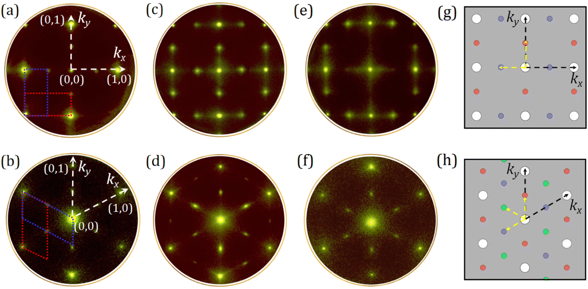 | ||
| Fig. 1 LEED patterns of the diamond (100) and (111) samples at various stages of preparation collected at a beam energy of 100 eV and 150 eV, respectively. (a) C(2 × 1)-(100) bare surface and (b) C(2 × 1)-(111) bare surface; (c) C(2 × 1)-(100):0.25 ML Sc and (d) C(2 × 1)-(111):0.25 ML Sc, both after deposition at RT, and (e) C(2 × 1)-(100):0.25 ML Sc and (f) C(2 × 1)-(111):0.25 ML Sc, both after in vacuo annealing to 900 °C. The (100) and (111) surfaces possess four-fold and three-fold symmetries resulting from two and three rotational diffraction domains with a commensurate topology of (2 × 1) or (1 × 2), respectively. The reciprocal-lattice vectors along the kx and ky axes are indicated by white dashed arrows, while blue- and red-dashed rectangles/parallelograms indicate (2 × 1) and (1 × 2) reconstructions, respectively. Diagrams are also shown for a superposition of the simulated reciprocal-space patterns for the (g) C(2 × 1)-(100):0.25 ML Sc and (h) C(2 × 1)-(111):0.25 ML Sc surfaces. In panel (g), two domains rotated by 90° in a square lattice are shown as blue and red circles for C and Sc atoms, respectively. In (h), three domains are rotated by 120° in a hexagonal lattice: blue is for C, while green and red circles are for Sc atoms. The white circles refer to the (1 × 1) spots, whilst black and yellow dashed arrows are the primitive reciprocal-lattice vectors representing (1 × 1) diffraction spots and (2 × 1) or (1 × 2) reconstructions, respectively. | ||
In contrast, as illustrated in Fig. 1(b), an extra domain appeared for the (111) surface due to the presence of unstable dangling bonds following H desorption, resulting in a constant (2 × 1) reconstruction. This led to the formation of Pandey or conjugated π-bonded chains from the surface carbon atoms on the upper- and lower-layer forming a corrugated surface.32 A reciprocal distance of three rotational domains in a hexagonal lattice was 1.25 Å−1 along the k-vectors, giving a real-space separation of 5.03 ± 0.02 Å (Fig. 1(b)).
Although homoepitaxial bare (100) and (111) surfaces are atomically flat and well ordered, as confirmed by EF-PEEM maps (see later), the absence or weaker intensity of some inner diffraction spots between the integral-order domains (i.e., between (0,0) and (0,1) or (1,0)) can be seen for the (100) and (111) diamond LEED patterns (Fig. 1(a) and (b)). This is most likely a result of scattering from the bare surface with a disordered top-most layer after in vacuo annealing at 920 °C;31 thus, the background intensity was fainter than that for the hydrogenated surfaces (Fig. S2(a) and (b)†). Meanwhile, a good indication of low defect density for the Sc-adsorbed surfaces can be obtained from Fig. 1(c) and (d), with the appearance of sharp half-order spots with low background intensity suggesting an excellent quality of the structural order at the surface layer. This is also evident from the spot-profile analysis of the bare and 0.25 ML Sc-adsorbed diamond (100) and (111) surfaces along the kx vector (see Fig. S4 in the ESI†). Although the individual spot intensities may differ, it is significant to note that the LEED spot positions associated with the bare C(100)-(2 × 1) and C(111)-(2 × 1) substrates remain intact after Sc deposition at room temperature (RT). Thus, the lattice constant of the topmost layer of both single-crystal (100) and (111) samples remains unaltered, allowing a 2D adsorption of the sub-ML of Sc.
Following annealing of the (100) and (111) surfaces at elevated temperatures (Fig. 1(e) and (f)), the 0.25 ML coverage of Sc was retained with a (2 × 1) surface reconstruction. The LEED patterns showed that the inner spots along the different axes (kx and ky) of the surface became more diffuse, with an increased streakier background compared to that in the diffraction pattern for the (1 × 1) reconstruction. Moreover, a slight decrease in the two-domain spacing to 1.25 Å−1 was observed for the (100) surface, while the reciprocal distance for the (111) sample remained stable. Respective real-space distances of two (100) and (111) samples provided a value of 5.03 Å ± 0.02 Å after annealing at 900 °C. These values agree well with our theoretical predictions and with those from other DFT studies,32 providing rectangular and parallelogram primitive unit cells with a lattice constant of 5.02 Å and 5.03 Å along the x-axis direction for the (100) and (111) surfaces, respectively (see Fig. 2(c) and (d)).
 | ||
| Fig. 2 The lowest-energy optimised geometries of the (a) C(2 × 1)-(100) and (b) C(2 × 1)-(111), and (c) C(2 × 1)-(100):0.25 ML Sc surface and (d) C(2 × 1)-(111):0.25 ML Sc surface calculated using DFT. The surface primitive unit cells are marked by blue dashed rectangles and parallelograms representing (2 × 1) reconstruction for the (100) and (111) surfaces, respectively. (e and f) Drawings of the superposition of real-space patterns for the C(2 × 1)-(100):0.25 ML Sc and C(2 × 1)-(111):0.25 ML Sc surfaces with square and rhombus grey grids, respectively. The red circles are the position of individual domains, whilst the blue dashed rectangle and parallelogram show the (2 × 1) periodicity. | ||
To support the experimental data, the LEED patterns for the 0.25 ML Sc-terminated diamond were constructed by the LEEDpat simulation, applying a matrix  with a set of blue and red spots referring to the two domains rotated by 90° for the (100) surface, and three domains including blue, green and red, related by 120° rotation on a hexagonal lattice for the (111) sample. The reciprocal unit-cell vectors for one of the Sc adatoms and the surface Cd atom are indicated in Fig. 1(g) and (h), while corresponding primitive unit-cell lattices are square and hexagonal, as expected for the single-crystal diamond (100) and (111), with a (2 × 1) reconstructed surface.
To evaluate the adsorbate site geometry resulting from the interaction of adatoms with diamond, electronic and structural properties of the bare and the 0.25 ML Sc-terminated boron-doped diamond (BDD) (100) and (111) surfaces were computed employing ab initio DFT calculations. The associated minimum-energy configurations for these surface terminations on the two diamond surfaces are shown in Fig. 2(a)–(d).
By applying Levin's model (primarily proposed for bare Si(100)), the possible structures with 0.25 ML surface coverage of Sc were calculated using a method previously reported for theoretical and experimental studies of alkali metals adsorbed onto diamond.36,37 With Levin's and other suggested models, most metal adsorbates generally occupy the hollow or cave sites leading to a (2 × 1) symmetry on Si or diamond, consistent with our recent DFT calculations for Al and Sc adsorbed onto undoped diamond (100).23,34 However, an ‘overlaid above-row configuration’ is also possible for TMs and some metalloids with a surface coverage of 0.25 ML, as observed for the Si(100) surface, where adsorbate atoms sit directly above the underlying dimer row.38–40 This adsorption geometry resembles a ‘pedestal-like’ structure and agrees with our experimental data if the as-deposited Sc atoms sit perpendicular to the direction of the bare C–C dimers in the topmost layer. In this configuration, the Sc adatom locally occupies the individual pedestal sites, lying on top of two parallel dimers. This adsorbate geometry was therefore confirmed by DFT calculations as the lowest-energy and most-negative EA configuration among the available adsorption sites for the 0.25 ML Sc-adsorbed boron-doped C(100)-(2 × 1) surface, as depicted in Fig. 2(c).
For the (111) surface, Sc adsorbs strongly at the hollow site of a lower chain on the bare surface with a surface coverage of 0.25 ML, providing a thermodynamically favourable configuration amongst others (Fig. 2(d)). However, the EA value of this structure is less negative than that of the cave site of a lower chain. A real-space pattern simulation was performed to accompany the DFT calculations, to provide a better understanding of the real-space structure. This resulted in the diagrams of surface reconstruction of (2 × 1) or (1 × 2) in a real-space lattice for the 0.25 ML Sc-terminated diamond (100) and (111) samples, as shown in Fig. 2(e) and (f), respectively.
Having examined the surface structure of Sc adsorption on the bare (100) and (111) diamond surfaces, we now turn to investigate the elemental composition and surface electronic states by core-level photoemission. To monitor chemical changes in C and Sc core-level peaks with no contamination present at the surface, XPS scans were performed in situ at various stages of the sample preparation.
To gain insights into the nature of surface bonding, the deconvoluted C 1s peak has been extensively studied in the context of functionalised diamond.29,41 For completeness, the deconvoluted XPS spectra for the (100) and (111) surfaces have been shown in the ESI† (Fig. S5) as benchmarks and provide evidence that the system calibration was performing as expected. For the spectra of the hydrogenated (100) and (111) surfaces, two separate chemical components can be found which are characteristic of bulk and surface C atoms with sp3 hybridisation, arising at binding energies (BEs) of 284.3 eV and ∼285 eV, respectively, no matter how the surface is terminated. Although the intensity of C 1s was slightly higher for the H-terminated (100) surface, core-level spectra for both hydrogenated surfaces were similar, with BEs of 284.19 eV and 284.27 eV for the C 1s bulk component (CB) of the C(2 × 1)-(100):H and C(1 × 1)-(111):H, respectively. The second component peak associated with the surface carbon (CS) was at ∼+0.6 eV relative to CB, indicating H-termination or existing hydrocarbon fragments.33,42
To determine the surface Fermi level (EF) states, Maier et al.43 calculated the fixed core-level BE separation between the bulk C 1s and the valence-band maximum (VBM) to be 283.9 eV. For the C(2 × 1)-(100):H and C(1 × 1)-(111):H surfaces, the EF position was thus pinned at 0.29 eV and 0.37 eV above the VBM position, respectively. These values vary with the doping level of samples, but are in close agreement with the positions of the bulk Fermi level, ranging between 0.20 eV and 0.40 eV.42 Thus, we infer that no additional band-bending is induced before the full desorption of H atoms. In addition, the calculated values of the VBM for both hydrogenated surfaces obtained by XPS analysis are further compared with the experimentally measured values from UPS scans (see Table 1).
| Diamond | VBM, eV | ϕ, eV | χ, eV | ||
|---|---|---|---|---|---|
| XPS | UPSa | UPS | EF-PEEM | ||
| a The determined values are indicated with a negative sign, as the Fermi level is set to zero. | |||||
| (2 × 1)-(100):H | 0.29 | 0.72 | 3.49 | 3.60 | −1.28 |
| (1 × 1)-(111):H | 0.37 | 0.89 | 3.62 | 3.74 | −0.96 |
| (2 × 1)-(100) | 0.96 | 1.06 | 4.94 | 5.13 | 0.53 |
| (2 × 1)-(111) | 1.04 | 1.12 | 5.03 | 5.18 | 0.68 |
| (2 × 1)-(100):0.25 ML Sc (as-deposited at RT) | 0.86 | 0.58 | 4.33 | 4.45 | −0.56 |
| (2 × 1)-(111):0.25 ML Sc (as-deposited at RT) | 0.98 | 0.64 | 4.59 | 4.73 | −0.24 |
| (2 × 1)-(100):0.25 ML Sc after annealing at 900 °C | 0.48 | 0.80 | 3.22 | 3.28 | −1.45 |
| (2 × 1)-(111):0.25 ML Sc after annealing at 900 °C | 0.60 | 0.82 | 3.52 | 3.58 | −1.13 |
Fig. 3 shows a set of normalised C 1s core-level spectra acquired for (i) the bare (100) and (111) diamond surfaces after in vacuo annealing at 920 °C, (ii) following Sc deposition of 0.25 ML coverage onto the bare (100) and (111) diamond (labelled ‘as-deposited’), and (iii) the 0.25 ML Sc-adsorbed bare C(100) and (111) surfaces after the final annealing stage at 900 °C. The 920 °C annealing under UHV causes H desorption and creates an adsorbate-free bare diamond surface. The chemical shifts of the core-level spectra for C 1s for this surface are consistent with an alteration of surface states leading to PEA with the conduction band minimum (CBM) situated below the vacuum level.25,33
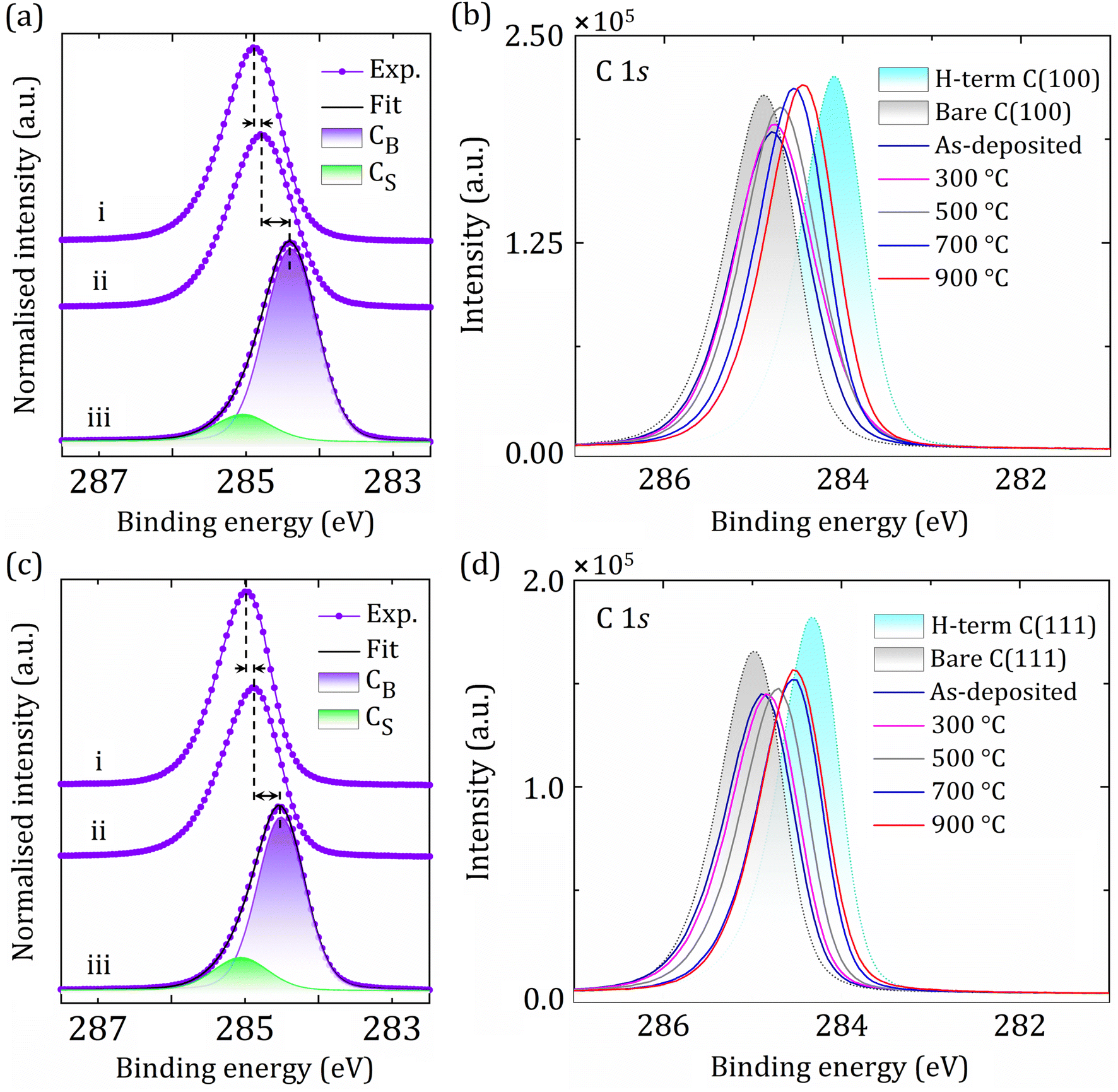 | ||
| Fig. 3 Core-level spectra of C 1s at specific processing stages (a and c) (e.g. (i) bare diamond after annealing, (ii) after 0.25 ML Sc deposition and (iii) after in vacuo annealing at 900 °C) of the sample preparation on the diamond (100) and (111) surfaces, respectively, from a set of spectra (b and d) for step-by-step acquisitions. Black dashed lines indicate peak positions, showing the binding energy (BE) shift of the C 1s peak. Bulk and surface carbon components are labelled CB and CS, respectively. | ||
The C 1s peaks are composed of bulk (CB) and surface (CS) carbon components, as depicted in Fig. 3. The formation of surface states and occurrence of band-bending are primarily influenced by shifts in the C 1s core-level BE, although other factors, such as peak shape and asymmetry also contribute to surface effects, as described elsewhere.25 By deposition of sufficiently electropositive Sc atoms with successive annealing steps, a continuous decrease in BE for the C 1s peak is observed by detailed step-by-step monitoring for both the (100) and (111) surfaces, although the CB component is independent of the surface modification (Fig. 3(a) and (c)). This behaviour is the opposite of that observed for other functionalised diamond surfaces exhibiting PEA reported earlier.30
In contrast, for both the (100)- and (111)-oriented samples, the BE for the Sc 2p peak continually increased with successive annealing steps, shifting chemically in the opposite direction relative to the C 1s peak (Fig. 4). For the as-deposited C(100) and (111), the Sc 2p3/2 sits at 398.56 eV and 398.49 eV, respectively, in excellent agreement with the literature, as observed for the metallic (or ScC) layer peak of Sc at 398.45 eV.44 Using the core-level spectral areas for Sc and CS, we estimate that ∼25% of the CS components become terminated with Sc. Specifically, the amount of the deposited Sc onto bare diamond was 25.2% and 24.6% for the (100) and (111) surfaces, respectively. This fraction is just slightly reduced during the annealing steps, suggesting that most of the adsorbed Sc atoms are strongly attached to the diamond surface.
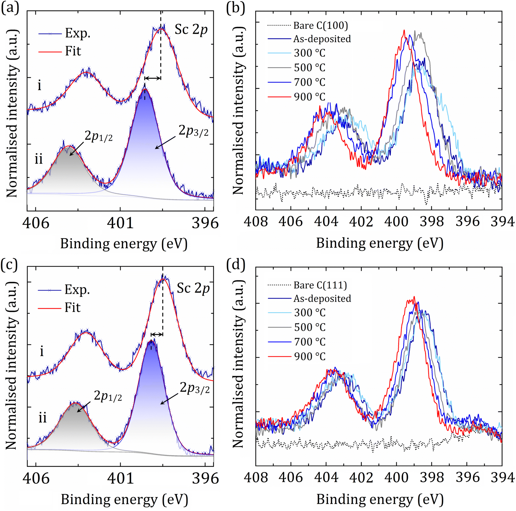 | ||
| Fig. 4 Core-level spectra of Sc 2p at specific analysis stages (a and c) (e.g. (i) after 0.25 ML Sc deposition and (ii) after in vacuo annealing at 900 °C) of the sample preparation on the diamond (100) and (111) samples, respectively, from a set of spectra (b and d) for step-by-step monitoring. Black dashed lines indicate peak positions for Sc 2p3/2, showing the BE shifts of the Sc 2p peak. | ||
Although all analyses were done in situ, it is significant that due to the high affinity of Sc towards oxygen, coupled with the known trace amount of O present within the Sc rod (see Table S1 in the ESI†), a small quantity of O was observed after Sc deposition for both surfaces. Similar behaviour has previously been described by Moram et al. for an ScN thin-layer on sapphire, indicating that there was a trace amount of Sc2O3 species present in their samples.45 This suggests that by using UHV conditions, O incorporation into the Sc-containing thin films can easily be limited to only trace amounts. As a result, the O 1s peak is present only after deposition but reduces following low-temperature annealing (300 °C and 500 °C), as reported by O'Donnell et al. for the Li–O–Cd system.13 The small amount of O had fully desorbed after the 700 °C annealing (Fig. S6†), leading to a more thermodynamically favourable configuration via a ‘scandium-oxycarbide’ to ‘scandium-carbide’ transition.
A complex shifting of carbon and scandium BEs in opposite directions causes a substantial increase in the surface dipole, suggesting the CBM is pinned a long way above the vacuum level, resulting in a high NEA (see the UPS spectra and WF maps later). For the Sc 2p peak, the final shift in BEs after the annealing at 900 °C was found to be +0.96 eV and +0.68 eV for the single-crystal diamond (100) and (111) surfaces, respectively. We interpret this as being due to a thermal ‘activation’ effect resulting in significant structural and electronic changes on both diamond surfaces. A detailed summary of fitting parameters for C 1s and Sc 2p core-level spectra is tabulated in Tables S2 and S3 in the ESI.†
The electrostatic potential results in charge imbalances in bonds (i.e. Sc–C bonds), accompanied by a BE shift of core-level electrons.30,46 With this in mind, we calculated the electrostatic potential acquired for the two diamond orientations for bare and 0.25 ML Sc-terminated diamond surfaces. Although the electrostatic potentials of these two surfaces are significantly different, the relative magnitude of the C 1s and Sc 2p core-level BE shifts for both the (100) and (111) single-crystal samples shows that they exhibit surface-dipole formation caused by the scandium addition onto the bare diamond. The Pauling electronegativity value of carbon (EN = 2.55) is higher than that for scandium (EN = 1.36), thus, the surface C atoms possess a slight negative charge when bonded to the deposited Sc, while a slight positive charge appears on the Sc atoms. This results in dipole formation on the diamond surface, with Sc sitting on the positive side of the surface dipole. In contrast, the negative side is situated on the uppermost C layer. Consequently, due to a significant charge transfer from the adsorbed Sc atoms, carbon and scandium core-level BEs shift in opposite directions during the thermal activation process.
While the BEs in core-level spectra are closely related to the atomic position of each element (e.g. C or Sc) in the potential plot, the overall shift of BE for the CB and CS components can be interpreted by the change of bulk (VB) or surface (VS) potentials from the bare surface to Sc-termination, respectively.30 Because the surface properties of functionalised diamond are of primary interest in this study, VS oscillations through the (100) and (111) surfaces from the simulated electrostatic plots (Fig. S7 in the ESI†) were compared with the BE shift of the CS component peak for each surface. The difference in VS values was −4.21 eV and −3.52 eV for the (100) and (111) samples, respectively, in reasonable agreement with our experimental results from XPS, where the CS peak shifted in BE to −0.42 eV for the (100) surface and −0.36 eV for the (111) surface (Table S2 in the ESI†). Thus, this suggests a qualitative confirmation that the surface C peak (CS) for (100) diamond shifts to a greater extent than for the (111) surface, indicating a larger surface dipole (or NEA).
We now focus on possible emission mechanisms from the Sc-adsorbed (100) and (111) diamond surfaces in an effort to unravel the change in EA or WF through an ‘activation’ process. Since the electronic states of the particular surface differ based on the position of its energy levels (e.g. EF and the vacuum level), we now consider three cases: PEA, NEA and ‘true’ NEA, and their relationship with the WF, as shown schematically in Fig. 5.
 | ||
| Fig. 5 Schematic band diagram illustrating the electron affinity, χ and its relationship with the work function, ϕ, in relation to a fixed vacuum energy level, Evac, for various semiconductor systems. The valence band (VB) and conduction band (CB) are represented in red and blue, respectively. The position of the Fermi level, EF, in the band gap varies depending upon the doping type of diamond. (a) PEA, (b) NEA, (c) ‘true’ NEA in p-doped diamond with downward band bending. | ||
For PEA, EF is typically situated midway between the upper level of the valence band (VB) and the lower level of the conduction band (CB), while Evac usually lies higher in energy than the CBM (ECBM). This allows any electrons excited into the CB by sufficient thermal energy or photoexcitation to overcome the surface potential barrier to escape and be emitted into the vacuum.
In contrast, for NEA, the CBM is higher in energy and is now situated above the vacuum level. Thus, any electrons in the CB can escape barrierless into the vacuum level, emerging with a significant kinetic energy value of a few eV, equal to the NEA (Fig. 5(b)).
Because the (100) and (111) diamond samples are both p-type doped in this study, EF is pinned close to the VBM with an energy difference of 0.29 eV and 0.37 eV, respectively (see the XPS section above), while the CB and VB are bent downwards at the surface, giving ‘true’ NEA, as shown in Fig. 5(c). However, if the downward band bending is significant, p-type diamond is unsuitable at the outset because of the necessity for electrons to overcome the large band gap to enter the CB. Thus, the energies required to excite and emit electrons may become achievable at moderate temperatures.7
For UPS analysis, the two H-terminated (100) and (111) samples were analysed first as benchmarks, as with the previous LEED and XPS studies, and compared with UPS spectra from the broader literature.25,30,47,48 The typical high-intensity peak emerging beside the CBM is found to originate from emitted electrons, as observed for both H-terminated (100) and (111) diamond, exhibiting characteristic features of an NEA surface (Fig. S8†). The measured EA values for these two hydrogenated surfaces were −1.28 eV and −0.96 eV, respectively, in excellent agreement with our DFT simulations and WF maps produced by EF-PEEM scans in this work (Table 1 and Fig. S9 in the ESI†) and those from previous experimental studies.25,43,47,48 For brevity, this paper focuses mainly on UPS and EF-PEEM results from the (100) diamond sample. However, the corresponding results and data for (111) diamond can be found in the ESI.†
Fig. 6(a) is a UPS spectrum displaying the energy distribution of inelastically scattered electrons (i.e. secondary electrons) for the (100) diamond sample, subdivided into four regions of interest, labelled I–IV. The lower and higher energy regions of the UPS spectra acquired after each sample preparation step are predominantly represented by the VB and CB states, respectively. Therefore, the VBM position (EVBM) is determined by linear extrapolation relative to EF of the curve in region I, as depicted in Fig. 6(b). Regions II and III correspond to σ states from the bulk diamond at 8 eV and 10 eV, respectively, as described earlier.32,49 Notably, with the addition of Sc and after the following annealing steps, these two peaks gradually moved to higher energy by ∼0.3 eV. Moreover, the photoemission intensity continually decreased from bare (100) diamond to annealed ‘activated’ Sc-terminated surfaces, while the EA values became more negative, suggesting a smooth transition to NEA.
 | ||
| Fig. 6 Region-selected UPS spectra at various stages of sample preparation (e.g. bare diamond, after the stages of 0.25 ML Sc deposition and in vacuo annealing up to 900 °C) on the diamond (100) surfaces. (a) UPS spectra labelled with four regions of interest. The regions labelled I and IV are depicted with red and blue rectangles, respectively. Corresponding magnified panels define the (b) VBM and (c) cut-off energy relative to the Fermi level, respectively. UPS spectra for the corresponding (111) diamond sample are provided in the ESI (Fig. S10).† | ||
The intense signal from secondary electrons is detected as a tail just above the CBM for the thermally ‘activated’ surfaces due to a higher electron density in the CB, implying inelastic electron–electron scattering during emission.50 The peak intensity after the 900 °C annealing stretches up to 1.45 eV below the CBM prior to reaching the vacuum energy at zero (see the electronic band structure for ‘true’ NEA in Fig. 6(c)). As a result, the electron emission below the CBM results from within the band gap regions, assigned to surface emissions owing to evanescent waves at the metal–vacuum interface.51 For both (100) and (111) surfaces, the peaks are more pronounced with each annealing step, with increasing cut-off energies in region IV, as depicted in Fig. 6(c). It is important to highlight that the most intense secondary-electron emission (SEE) peak for the (100) surface after 900 °C annealing was slightly higher than that for the hydrogenated (100) surface (see Fig. S8 in the ESI†) and more than twice the height of the peak from the (111) surface (Fig. S10 in the ESI†).
Fig. 6(c) provides information on the cut-off energy after each step of the sample preparation. The difference between the energy of the He(I) photon source (21.22 eV) and the cut-off energy is therefore defined as the WF, ϕ, for the surface of interest (in this case, for PEA surfaces) from the UPS study. Using the energy difference between EF and EVBM within the UPS spectrum, the EA, χ, is therefore calculated from
| χ = ϕ + (EF − EVBM) − Eg | (1) |
However, for NEA surfaces, the presence of an extra peak for SEE complicates the direct determination of the WF by the conventional UPS method. Therefore, other surface-sensitive techniques like EF-PEEM are preferred for this measurement. To do so, real-space WF acquisitions across the surface were constructed into a map through a pixel-by-pixel selection of EF-PEEM images in an area of interest. For each pixel of the image, the photoemission threshold, I, is determined using the eqn (2):52
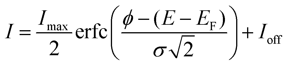 | (2) |
The average WF values from colour-coded WF maps for the diamond (100) surface are shown in Fig. 7. Compared to UPS scans, averaging the WF across the surface of both single-crystal samples provides only approximate values. This is likely due to scanning over a few dozen μm surface area by EF-PEEM. The discrepancy in experimental results between these two methods is up to 3.7%, which suggests that the measured values are reasonably consistent. The determined WF values using two different techniques (i.e. UPS and EF-PEEM) are compared in Table 1 alongside the VBM. The position of the VBM, which is a necessary input for the calculation of EA through eqn (1), was also derived from two techniques: Maier's method (see the XPS section) and linear extrapolation from the UPS spectra.
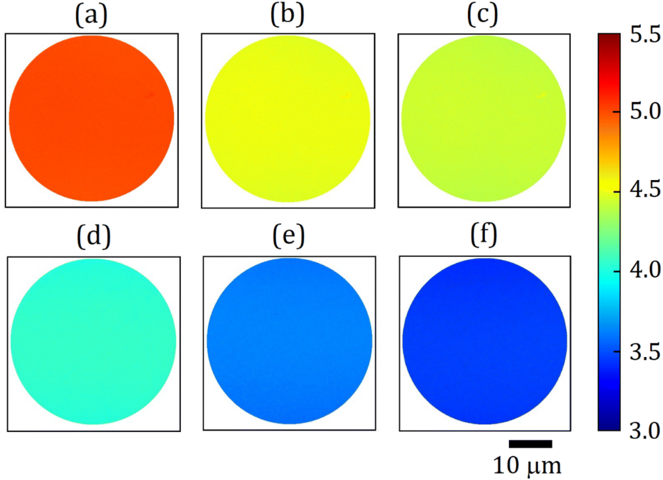 | ||
| Fig. 7 Colour-coded WF maps at various stages of the sample preparation ((a) 0.25 ML Sc-terminated bare (100) diamond, and annealing at (b) RT, (c) 300 °C, (d) 500 °C, (e) 700 °C and (f) 900 °C). The field of view for all WF maps is 37.5 μm. | ||
A gradual decrease from a value of ∼5.13 ± 0.02 eV for bare diamond to 3.28 ± 0.02 eV following the final annealing of the 0.25 ML Sc-terminated diamond (100) at 900 °C, respectively, occurs as illustrated in Fig. 7(a)–(f). Unlike metal adsorbates on oxygenated diamond reported previously,10,11 the exceptional quality of these WF maps indicates a remarkably highly uniform surface without 2D islands or 3D clusters of Sc, in agreement with our DFT predictions.23 Such uniform surface properties obtained from Sc-adsorbed bare diamond surpass those from the hydrogenated surface, producing a high SEE yield useful for numerous electron-emission devices. The corresponding WF maps for Sc-terminated (111) diamond are given in Fig. S11 in the ESI† and show a similar decrease in WF from ∼5.18 ± 0.02 eV to 3.58 ± 0.02 eV under the same conditions.
DFT calculated and experimentally determined EA values for the bare, hydrogenated and 0.25 ML Sc-terminated diamond (100) and (111) surfaces are summarised in Table 2, and compared with those from other theoretical and experimental work. Theoretical calculation of EA values was performed as previously described by our group.23 Although all computed EA magnitudes are considerably higher than their corresponding experimental values for both (100) and (111) surfaces, the substitutional B-doped structures clearly possess a downward band-bending, providing predicted DFT values that are closer to the experimental ones than those from undoped diamond calculations.23
| Diamond | DFT computed χ, eV | Measured χ, eV | Source |
|---|---|---|---|
| a The calculated values are for undoped diamond surfaces. | |||
| (2 × 1)-(100):H | −1.68 | −1.28 | This study |
| −1.94a | −1.30 | 23 and 43 | |
| (1 × 1)-(111):H | −1.51 | −0.96 | This study |
| −2.00a | −0.90 | 25 and 53 | |
| (2 × 1)-(100) | 0.48 | 0.53 | This study |
| 0.65a | 0.50 | 23 and 54 | |
| (2 × 1)-(111) | 0.42 | 0.68 | This study |
| 0.35a | 0.50 | 53 and 54 | |
| (2 × 1)-(100):0.25 ML Sc after annealing at 900 °C | −1.97 | −1.45 | This study |
| −3.02a | — | 23 | |
| (2 × 1)-(111):0.25 ML Sc after annealing at 900 °C | −1.47 | −1.13 | This study |
The most negative EA value for 0.25 ML Sc on the bare diamond (100) surface is determined from the UPS analysis, using eqn (1), to be −1.45 eV. To the best of our knowledge, this is the largest NEA value for any metal–diamond surface studied to date. In contrast, for the 0.25 ML Sc-adsorbed bare diamond (111) surface, the experimental EA value is measured to be −1.13 eV. This value is slightly higher than that of the hydrogenated diamond (111) surface, however, unlike the latter, the Sc-terminated sample remains stable throughout the annealing steps at elevated temperatures up to 900 °C, providing a highly ordered uniform surface, as shown by the WF maps (see Fig. 7).
4. Conclusion
We carried out an experimental study of EA and WF for 0.25 ML Sc-terminated bare diamond with two different crystal (100) and (111) orientations. A three-step UHV process was used to prepare the samples, starting with the high-temperature desorption of H atoms from the hydrogenated diamond surface to produce bare diamond, followed by Sc deposition at room temperature, and finally thermal annealing up to 900 °C. Analysis of these Sc–diamond (100) and (111) samples with UPS and EF-PEEM revealed the most negative EA values yet measured for a metal–diamond system of −1.45 eV and −1.13 eV, respectively. The corresponding WF values by UPS for these two surfaces were 3.22 eV and 3.52 eV, while the EF-PEEM maps showed the surface electronic properties to be homogeneous and uniform over a scale of a few dozen μm.For comparison, the electronic and structural properties of these two Sc-terminated diamond (100) and (111) surfaces were calculated using ab initio DFT modelling, which predicted slightly higher EA values of −1.97 eV and −1.47 eV, respectively. This is probably due to limitations in the DFT modelling, such as underestimation of the band gap (a well-known problem with GGA functionals) or the inaccuracy of representing p-type doping by B atoms being added to the model diamond stack.
In addition to the large NEA and small WF values for these Sc-terminated surfaces, the important finding is that these properties did not degrade after annealing at temperatures up to 900 °C. Thus, we suggest that these 0.25 ML Sc-terminated bare diamond (100) and (111) surfaces are possibly the most promising system reported so far for electron emission from diamond, affording a high electron-emission yield at low temperatures (∼500 °C) without degrading during use, and which are compatible with commercial TECs for solar power applications. Further work on and optimisation of this Sc–diamond system, for example, with respect to different coverages (half ML or full ML), annealing temperatures or durations, could be done to improve the NEA and WF further. Also, for optimal electron emission, the use of an n-doped diamond substrate might aid the transfer of electrons into the VB.
Data availability
Further details of these calculations can be found in the ESI.† The raw data for these experiments can be found in the University of Bristol data repository, data.bris, at https://doi.org/10.5523/bris.2siu0761brbd2aprfb1cuw010.Author contributions
Ramiz Zulkharnay: conceptualisation, methodology, software, formal analysis, investigation, writing – original draft, visualisation. Paul W. May: methodology, resources, validation, review & editing, supervision.Conflicts of interest
The authors declare that they have no known competing financial interests or personal relationships that could have influenced the work reported in this paper.Acknowledgements
RZ wishes to acknowledge the funding scheme of the Government of the Republic of Kazakhstan under the Bolashak International program. The authors acknowledge the use of the University of Bristol NanoESCA facility. DFT calculations were carried out using the BlueCrystal Phase 4 high-performance computing cluster of the Advanced Computing Research Centre, University of Bristol.References
- G. B. Asheim, T. Fæhn, K. Nyborg, M. Greaker, C. Hagem, B. Harstad, M. O. Hoel, D. Lund and K. E. Rosendahl, Science, 2019, 365, 325–327 CrossRef CAS PubMed.
- M. Meinshausen, N. Meinshausen, W. Hare, S. C. B. Raper, K. Frieler, R. Knutti, D. J. Frame and M. R. Allen, Nature, 2009, 458, 1158–1162 CrossRef CAS PubMed.
- M. R. Allen, D. J. Frame, C. Huntingford, C. D. Jones, J. A. Lowe, M. Meinshausen and N. Meinshausen, Nature, 2009, 458, 1163–1166 CrossRef CAS PubMed.
- D. M. Trucchi, A. Bellucci, M. Girolami, P. Calvani, E. Cappelli, S. Orlando, R. Polini, L. Silvestroni, D. Sciti and A. Kribus, Adv. Energy Mater., 2018, 8, 1802310 CrossRef.
- M. F. Campbell, T. J. Celenza, F. Schmitt, J. W. Schwede and I. Bargatin, Adv. Sci., 2021, 8, 2003812 CrossRef PubMed.
- G. Xiao, G. Zheng, M. Qiu, Q. Li, D. Li and M. Ni, Appl. Energy, 2017, 208, 1318–1342 CrossRef.
- M. C. James, F. Fogarty, R. Zulkharnay, N. A. Fox and P. W. May, Carbon, 2021, 171, 532–550 CrossRef CAS.
- W. F. Paxton, M. Howell, W. P. Kang and J. L. Davidson, J. Vac. Sci. Technol., B: Nanotechnol. Microelectron.: Mater., Process., Meas., Phenom., 2012, 30, 021202 Search PubMed.
- A. Croot, G. Wan, A. Rowan, H. D. Andrade, J. A. Smith and N. A. Fox, Front. Mech. Eng., 2017, 3, 1–8 Search PubMed.
- M. C. James, M. Cattelan, N. A. Fox, R. F. Silva, R. M. Silva and P. W. May, Phys. Status Solidi B, 2021, 258, 2100027 CrossRef CAS.
- F. Fogarty, N. A. Fox and P. W. May, Funct. Mater., 2022, 2, 103–111 Search PubMed.
- K. M. O'Donnell, T. L. Martin, N. A. Fox and D. Cherns, Phys. Rev. B: Condens. Matter Mater. Phys., 2010, 82, 115303 CrossRef.
- K. M. O'Donnell, M. T. Edmonds, J. Ristein, A. Tadich, L. Thomsen, Q.-H. Wu, C. I. Pakes and L. Ley, Adv. Funct. Mater., 2013, 23, 5608–5614 CrossRef.
- K. M. O'Donnell, T. L. Martin and N. L. Allan, Chem. Mater., 2015, 27, 1306–1315 CrossRef.
- K. M. O'Donnell, M. T. Edmonds, A. Tadich, L. Thomsen, A. Stacey, A. Schenk, C. I. Pakes and L. Ley, Phys. Rev. B: Condens. Matter Mater. Phys., 2015, 92, 035303 CrossRef.
- W. E. Pickett, Phys. Rev. Lett., 1994, 73, 1664–1667 CrossRef CAS PubMed.
- A. K. Tiwari, J. P. Goss, P. R. Briddon, A. B. Horsfall, N. G. Wright, R. Jones and M. J. Rayson, Europhys. Lett., 2014, 108, 46005 CrossRef.
- T. Tachibana, J. T. Glass and R. J. Nemanich, J. Appl. Phys., 1993, 73, 835–842 CrossRef CAS.
- P. K. Baumann and R. J. Nemanich, Phys. Rev. B: Condens. Matter Mater. Phys., 1998, 58, 1643–1654 CrossRef CAS.
- P. K. Baumann and R. J. Nemanich, Diamond Relat. Mater., 1998, 7, 612–619 CrossRef CAS.
- J. van der Weide and R. J. Nemanich, Phys. Rev. B: Condens. Matter Mater. Phys., 1994, 49, 13629–13637 CrossRef CAS PubMed.
- J. van der Weide and R. J. Nemanich, J. Vac. Sci. Technol., B: Nanotechnol. Microelectron.: Mater., Process., Meas., Phenom., 1992, 10, 1940–1943 CrossRef CAS.
- R. Zulkharnay, N. L. Allan and P. W. May, Carbon, 2022, 196, 176–185 CrossRef CAS.
- A. K. Tiwari, J. P. Goss, P. R. Briddon, N. G. Wright, A. B. Horsfall and M. J. Rayson, Phys. Rev. B: Condens. Matter Mater. Phys., 2012, 86, 155301 CrossRef.
- L. Diederich, O. M. Küttel, P. Aebi and L. Schlapbach, Surf. Sci., 1998, 418, 219–239 CrossRef CAS.
- K. E. Hermann and M. A. V. Hove, LEEDpat, V. 4.2, Berlin/Hong Kong, 2014, see also, http://www.fhi-berlin.mpg.de/KHsoftware/LEEDpat/index.html Search PubMed.
- S. J. Clark, M. D. Segall, C. J. Pickard, P. J. Hasnip, M. I. J. Probert, K. Refson and M. C. Payne, Z. Kristallogr., 2005, 220, 567–570 CAS.
- S. Zhao and K. Larsson, J. Phys. Chem. C, 2014, 118, 1944–1957 CrossRef CAS PubMed.
- G. T. Williams, S. P. Cooil, O. R. Roberts, S. Evans, D. P. Langstaff and D. A. Evans, Appl. Phys. Lett., 2014, 105, 061602 CrossRef.
- G. Wan, M. Cattelan and N. A. Fox, J. Phys. Chem. C, 2019, 123, 4168–4177 CrossRef CAS.
- M. Nishitani-Gamo, K. P. Loh, I. Sakaguchi, T. Takami, I. Kusunoki and T. Ando, J. Vac. Sci. Technol., A, 1999, 17, 2991–3002 CrossRef CAS.
- B. P. Reed, M. E. Bathen, J. W. R. Ash, C. J. Meara, A. A. Zakharov, J. P. Goss, J. W. Wells, D. A. Evans and S. P. Cooil, Phys. Rev. B: Condens. Matter Mater. Phys., 2022, 105, 205304 CrossRef CAS.
- R. Graupner, F. Maier, J. Ristein, L. Ley and C. Jung, Phys. Rev. B: Condens. Matter Mater. Phys., 1998, 57, 12397–12409 CrossRef CAS.
- M. C. James, A. Croot, P. W. May and N. L. Allan, J. Phys.: Condens. Matter, 2018, 30, 235002 CrossRef PubMed.
- G. Jnawali, H. Hattab, B. Krenzer and M. Horn von Hoegen, Phys. Rev. B: Condens. Matter Mater. Phys., 2006, 74, 195340 CrossRef.
- M. Z. Hossain, T. Kubo, T. Aruga, N. Takagi, T. Tsuno, N. Fujimori and M. Nishijima, Diamond Relat. Mater., 2000, 9, 162–169 CrossRef CAS.
- J. L. Nie, H. Y. Xiao, X. T. Zu and F. Gao, Chem. Phys., 2006, 326, 308–314 CrossRef CAS.
- C. Calandra, O. Bisi and G. Ottaviani, Surf. Sci. Rep., 1985, 4, 271–364 CrossRef.
- J. Wasserfall and W. Ranke, Surf. Sci., 1995, 331–333, 1099–1104 CrossRef CAS.
- S. J. Jenkins, G. P. Srivastava, R. J. Dixon and C. F. McConville, Surf. Sci., 1998, 402–404, 645–648 CrossRef CAS.
- S. Ghodbane, D. Ballutaud, A. Deneuville and C. Baron, Phys. Status Solidi A, 2006, 203, 3147–3151 CrossRef CAS.
- M. T. Edmonds, M. Wanke, A. Tadich, H. M. Vulling, K. J. Rietwyk, P. L. Sharp, C. B. Stark, Y. Smets, A. Schenk, Q.-H. Wu, L. Ley and C. I. Pakes, J. Chem. Phys., 2012, 136, 124701 CrossRef CAS PubMed.
- F. Maier, J. Ristein and L. Ley, Phys. Rev. B: Condens. Matter Mater. Phys., 2001, 64, 165411 CrossRef.
- M. C. Biesinger, L. W. M. Lau, A. R. Gerson and R. S. C. Smart, Appl. Surf. Sci., 2010, 257, 887–898 CrossRef CAS.
- M. A. Moram, Z. H. Barber and C. J. Humphreys, Thin Solid Films, 2008, 516, 8569–8572 CrossRef CAS.
- J. Blomquist, J. Electron Spectrosc. Relat. Phenom., 1985, 36, 69–76 CrossRef CAS.
- C. Bandis and B. B. Pate, Surf. Sci., 1996, 350, 315–321 CrossRef CAS.
- L. Diederich, P. Aebi, O. M. Küttel and L. Schlapbach, Surf. Sci., 1999, 424, L314–L320 CrossRef CAS.
- K. M. O'Donnell, T. L. Martin, M. T. Edmonds, A. Tadich, L. Thomsen, J. Ristein, C. I. Pakes, N. A. Fox and L. Ley, Phys. Status Solidi A, 2014, 211, 2209–2222 CrossRef.
- G. Wan, A. Croot, N. A. Fox and M. Cattelan, Adv. Funct. Mater., 2021, 31, 2007319 CrossRef CAS.
- R. F. Willis and N. E. Christensen, Phys. Rev. B: Condens. Matter Mater. Phys., 1978, 18, 5140–5161 CrossRef CAS.
- H. Dominguez-Andrade, M. Z. Othman, K. M. O'Donnell, J. H. Lay, P. W. May, N. A. Fox, J. Morin and O. Renault, Int. J. Nanotechnol., 2014, 11, 796–807 CrossRef.
- J. Robertson and M. J. Rutter, Diamond Relat. Mater., 1998, 7, 620–625 CrossRef CAS.
- P. K. Baumann and R. J. Nemanich, Surf. Sci., 1998, 409, 320–335 CrossRef CAS.
Footnote |
| † Electronic supplementary information (ESI) available. See DOI: https://doi.org/10.1039/d2ta09199b |
| This journal is © The Royal Society of Chemistry 2023 |