
Few-layer MoS2 nanosheets with and without silicon nanoparticles as anodes for lithium-ion batteries†
Ifra
Marriam
 *ab,
Mike
Tebyetekerwa
c,
Hao
Chen
a,
Hiran
Chathuranga
ab,
Nunzio
Motta
bd,
Jose A.
Alarco
bd,
Zhen-Jiang
He
e,
Jun-Chao
Zheng
e,
Aijun
Du
bd and
Cheng
Yan
*ab
*ab,
Mike
Tebyetekerwa
c,
Hao
Chen
a,
Hiran
Chathuranga
ab,
Nunzio
Motta
bd,
Jose A.
Alarco
bd,
Zhen-Jiang
He
e,
Jun-Chao
Zheng
e,
Aijun
Du
bd and
Cheng
Yan
*ab
aSchool of Mechanical, Medical, and Process Engineering, Faculty of Engineering, Queensland University of Technology, 2 George Street, Brisbane, QLD 4000, Australia. E-mail: ifra.marriam@hdr.qut.edu.au; c2yan@qut.edu.au
bCentre for Materials Science, Queensland University of Technology, 2 George Street, Brisbane, QLD 4000, Australia
cDow Centre for Sustainable Engineering Innovation, School of Chemical Engineering, The University of Queensland, St. Lucia, Brisbane, QLD 4072, Australia
dSchool of Chemistry and Physics, Queensland University of Technology, 2 George Street, Brisbane, QLD 4000, Australia
eSchool of Metallurgy and Environment, Central South University, Changsha, Hunan 410083, China
First published on 5th January 2023
Abstract
Few-layer two-dimensional (2D) molybdenum disulfide (MoS2) nanosheets are potential anode materials for lithium-ion batteries due to their stable electrochemical performance. On the other hand, silicon (Si) is attracting the attention of battery research due to its high specific capacity, but its problem of volume expansion remains a challenge. Hence, rationally designed MoS2 nanosheets with Si may take the synergy between these materials, which can not only mitigate the volume expansion but also maintain excellent electrochemical properties. Therefore, we have successfully synthesized few-layer MoS2 nanosheets on water-soluble, naturally abundant, and cost-effective recrystallized three-dimensional sodium chloride (NaCl) crystals. The obtained free-standing few-layer MoS2 nanosheets are utilized to form a MoS2@Si heterostructure. It has been confirmed that the layered MoS2 nanosheets can accommodate the volume expansion of Si and provide channels for lithium-ion transport during electrochemical cycles. After 500 cycles, the volume expansion is reduced to 68%, a remarkable improvement compared to 430% in pristine Si. Exceptional rate and cycling performance have been achieved in the composite anode, with a capacity retention of 60% compared to 0.3% for pristine Si at a high current density of 500 mA g−1. This work provides a rational design for Si and 2D material composites as anode materials for improved electrochemical performance.
Introduction
Two-dimensional (2D) layered materials are currently being considered for energy storage applications, commonly in batteries and supercapacitors, due to their unique electrochemical properties.1,2 These materials are from various sources with several properties. They include carbonaceous materials such as graphite (graphene), transition metal dichalcogenides (MoS2, WS2, MoSe2, WSe2, etc.), mono-element 2D materials (such as silicene, phosphorene, etc.), transition metal carbide- and carbon nitride-based MXenes, and many other materials such as metal–organic frameworks.3–6 This is because 2D materials have unique 2D intrinsic surface areas, which can easily facilitate fast and superior charge storage in batteries when exposed to electrolyte ions.7,8 In lithium-ion batteries (LiBs), graphite with a theoretical specific capacity of 372 mA h g−1 is popular and is currently employed as the commercial anode material.9–11 However, the limited capacity of graphite is a challenge, prompting research to hunt for new materials like silicon (Si) and metal oxides, which demonstrate higher storage capacities due to their alloying mechanism of charge storage.12 Si anodes are well known for their high initial capacities of ∼3500 mA h g−1 when tested at low current densities, but they retain minimal capacity at higher current densities. Also, notably, Si undergoes large volume fluctuation during the lithiation/delithiation, which can cause the pulverization of electrode materials resulting in severe capacity decay and unstable cycling performance.13,14 One approach to solving this problem is introducing other materials with the Si anode to suppress its volume expansion. Ideally, the added material should be electrochemically active, which can simultaneously contribute to the overall capacity.The addition of existing 2D materials can enhance the capacity of LiBs, given their good electrochemical properties and the tendency to suppress the volume expansion of Si particles, thus facilitating long cycle life.15,16 Among other 2D materials, MoS2 2D nanosheets are quite promising as an anode for LiBs. The experimental reversible specific capacity of the MoS2 anode reaches 1290 mA h g−1, and it exhibits excellent rate performance and lower cycling degradation.17,18 It has the capability of being cycled at high current densities with significantly less volumetric expansion upon lithiation.19,20 Hence, we designed a layer-by-layer heterostructure with MoS2 2D nanosheets and Si nanoparticles (MoS2@Si), i.e., MoS2–Si–MoS2, where few-layer MoS2 nanosheets wrap Si nanoparticles to suppress its volume expansion and improve the cycling stability of the anode during lithiation/delithiation.
However, obtaining few-layer MoS2 nanosheets is not a straightforward approach. Several techniques have been proposed to synthesize MoS2 nanosheets. They are commonly synthesized on thin substrates/wafers of Si/SiO2, glass, sapphire, etc.21–23 But it is challenging to transfer MoS2 nanosheets from these substrates without damaging their structure. Not only that, but the mass production of mono-to few-layer MoS2 is not possible because of the limited surface area of these substrates. Hence, we utilized a naturally abundant, cost-effective, water-soluble three-dimensional substrate (i.e., sodium chloride (NaCl) crystals) to synthesize few-layer MoS2 2D nanosheets via the chemical vapor deposition (CVD) technique. NaCl crystals are known to be highly effective in promoting the growth of MoS2 during the CVD process24–27 and are water soluble and environment friendly, allowing the easy removal of the salt substrate by simply dissolving in water to obtain neat MoS2 2D nanosheets. This avoids unnecessary contamination and irreversible damage to 2D nanosheets.
In this work, we synthesized continuous few-layer MoS2 2D nanosheets on a NaCl substrate, which are used to fabricate the MoS2@Si heterostructure via a vacuum filtration technique. The pristine MoS2 2D nanosheets and MoS2@Si heterostructure were then tested as anode materials for LiBs. The electrodes prepared with MoS2@Si demonstrated excellent electrochemical performance, greatly improved cycling stability after 500 cycles, and suppressed volume expansion of Si.
Experimental
Synthesis of MoS2 2D nanosheets
10 g of commercial NaCl (sodium chloride) (99%, Mw = 58.44 g mol−1, Sigma-Aldrich) were dissolved in 40 ml of distilled water to form a saturated solution and filtered through vacuum filtration. Then, 20 ml of ethanol was added to the filtered solution to promote the crystallization of NaCl crystals. The solution was stirred well and filtered again. Then, the filtered NaCl crystals were dried in an oven at 80 °C overnight, and the micron-sized NaCl cubes were obtained. The MoS2 2D nanosheets were then synthesized on NaCl cubes via the CVD technique. It begins by mixing MoO3 (molybdenum trioxide, 99.97%, Mw = 143.94 g mol−1, Sigma-Aldrich) with a trace amount of NaCl (20 wt%) as a growth promoter to promote the volatilization of Mo precursor at low temperatures. The growth is performed in a two-zone furnace at a low-pressure (0.05 MPa) equipped with a 15 cm quartz tube. Zone 1 contained sulfur as a precursor (99.97%, Mw = 32.07 g mol−1, Sigma-Aldrich) with a temperature of 150 °C. At the same time, the MoO3 + NaCl mixture and crystallized NaCl (as a substrate) were placed in zone 2 with a temperature of 700 °C. Noble gas (Ar) with the 80 sccm flow was introduced in the CVD chamber tube. The chamber was then heated at 70 °C min−1. Three different growth times, 3, 5, and 10 min were set to observe their effect on the growth of MoS2.Fabrication of the MoS2@Si heterostructure
A sandwich heterostructure of MoS2 2D nanosheets with 0D Si nanoparticles (MoS2@Si) was prepared via vacuum filtration. First, MoS2@NaCl was dissolved in distilled water and centrifuged at 13![[thin space (1/6-em)]](https://www.rsc.org/images/entities/char_2009.gif) 000 rpm until the NaCl was completely dissolved. Simultaneously, Si was prepared in solution by mixing Si powder (98%, ≤50 nm, Sigma-Aldrich) with distilled water, followed by stirring until a uniform dispersion was achieved. The MoS2 and Si solutions with a ratio of 1:1 were poured to form a layer-by-layer assembly of MoS2@Si through the vacuum filtration process.
000 rpm until the NaCl was completely dissolved. Simultaneously, Si was prepared in solution by mixing Si powder (98%, ≤50 nm, Sigma-Aldrich) with distilled water, followed by stirring until a uniform dispersion was achieved. The MoS2 and Si solutions with a ratio of 1:1 were poured to form a layer-by-layer assembly of MoS2@Si through the vacuum filtration process.
Materials characterization
Raman spectra were recorded at room temperature using a RENISHAW inVia Raman spectroscope with a 532 nm edge filter laser beam as the excitation source. X-ray photoelectron spectroscopy (XPS) analysis was carried out using a Kratos AXIS supra photoelectron spectrometer with a monochromatic Al Kα source (1486.7 eV) at a power of 225 W and 15 mA emission current, and the obtained data were analyzed using the CasaXPS software version 2.3.24. The SEM morphology and EDS mapping of the samples were obtained using field-emission scanning electron microscopy (SEM, Tescan MIRA) at an acceleration voltage of 5 kV in secondary electron mode. Nitrogen adsorption/desorption isotherms were obtained on a Tristar II 3020 physisorption analyzer at 77 K. Prior to measurement, samples were degassed at 120 °C for 7 h.Electrochemical measurement
To check the electrochemical performance, the synthesized MoS2 2D nanosheets, the MoS2@Si composite, and Si powder were used as active materials to fabricate the electrodes for Li-ion batteries. The slurry was prepared by manual mixing of the active materials, carbon black (electrical conductor), and binder (carboxymethyl cellulose (CMC)) with a mass ratio of 6:2:2 in a solvent (distilled water). All the ingredients were mixed carefully with a hand grinder. The as-prepared electrode films were punched into 12 mm diameter circular disks and directly used as the working electrode in coin cells. The average areal mass loading of the active materials is around 1.6 mg cm−2. The standard coin cells (CR2032) were assembled in an argon-filled glovebox (O2 ≤ 0.1 ppm and H2O ≤ 0.1 ppm), using MoS2@Si, MoS2, and Si electrodes as working electrodes and lithium metal chips (0.45 × 15.6 mm, Gelon Energy Corp) as the counter-electrode. An insulating separator (2325 Celgard PP membrane) was used to prevent short-circuiting of the cell and 1.0 M LiPF6 in EC/DEC (LP40, BASF) with 50/50 (v/v) was used as the electrolyte. The electrochemical measurements (galvanostatic charge/discharge experiments) were performed on a Battery Testing System (CT-4008 NEWARE). The assembled cells were cycled over a potential range of 0.01–3 V (for MoS2 and MoS2@Si) and 0.01–1 V (for Si) vs. Li/Li+. The specific capacity was calculated on the basis of the active material only. The lithiation process was named the discharge process, and the de-lithiation process was indexed as the charge process. For the rate performance test, the anodes were first cycled at a lower current density of 20 mA g−1 for 10 cycles. The cyclic voltammetry (CV) behavior was tested on an EC-Lab potentiostat/galvanostatic instrument (VMP-300 BioLogic) with a scan rate of 0.1 mV s−1 in a voltage window of 0.01–3 V vs. Li/Li+.
Results & discussion
Materials analysis
The MoS2 nanosheets with 2D morphology offer high surface area and provide additional reactive sites for Li-ion storage.28 Also, large defect sites and void spaces between the 2D nanosheets allow the fast diffusion of Li-ions. Therefore, to synthesize the 2D MoS2 nanosheets, we used the CVD technique as illustrated in the schematic in Fig. 1A with temperature control according to Fig. S1,† with 3D crystallized NaCl cubes (Fig. 1B) employed as the substrate. NaCl is readily soluble in water; therefore, pristine MoS2 nanosheets can be obtained without damaging their structure. Fig. 1C–D show the MoS2 grown on the NaCl crystal surface. The color of the NaCl crystal turned from the original white to dark green after CVD growth (Fig. S2†) due to the presence of MoS2. The thickness and layer number were varied by controlling the time of MoS2 growth in the CVD chamber ranging from 2 to 10 minutes. Raman spectroscopy was employed to confirm the successful growth of MoS2 and to probe the relative difference between the layer numbers. As shown in Fig. 1E, the MoS2 on NaCl crystals (MoS2@NaCl) showed typical MoS2 Raman modes of E2g1 and A1g at ∼384 cm−1 and ∼409 cm−1, respectively. The E2g1 mode signifies the in-plane and A1g defines out-of-plane opposite vibrations of the Mo and S atoms.25,29 The opposing vibrations of the Mo and S atoms but parallel to each other are explained as the in-plane vibration mode, whereas the vibrations of the two S atoms in opposite directions are known as the out-of-plane mode.30,31 The Raman intensity of both vibration modes is proportional to the layer number, which can be achieved by increasing the growth time, as shown in Fig. 1E and S3.† The growth time, therefore, influences the amount and size of the MoS2 nanosheets, similar to previous reports.32 We also attempted to grow MoS2 nanosheets directly onto the Si nanoparticles but could not obtain well-defined 2D structures, despite being able to obtain MoS2 on Si (Fig. S4†). Further, the chemical composition of prepared MoS2 on NaCl was studied with the XPS technique (Fig. 1F–H). The wide XPS spectra of the MoS2 nanosheets in Fig. 1F show the prominent peaks of Mo and S elements which further proves the successful synthesis of MoS2. In the high-resolution XPS spectrum of Mo 3d, the two main peaks, Mo 3d5/2 and Mo 3d3/2, are observed at the binding energies of ∼229 eV and ∼232 eV (Fig. 1G) and confirm the presence of Mo4+ atoms. A minor peak at ∼226 eV next to the Mo 3d region corresponds to S 2s.33,34 Meanwhile, the double 2p peaks of S at ∼162 eV and ∼163 eV (Fig. 1H), which are recognized as the S 2p3/2 and S 2p1/2, respectively, indicate the S2− state of MoS2.35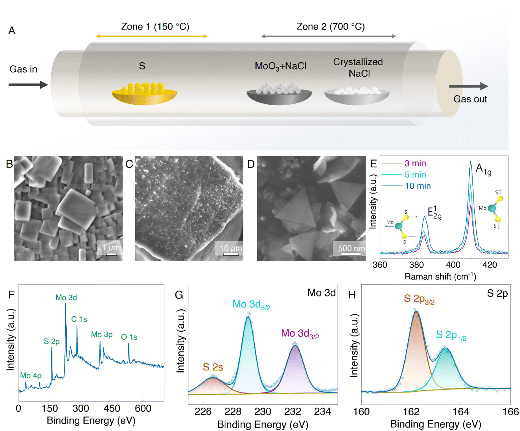 | ||
| Fig. 1 Growth and materials characterization of as-grown MoS2@NaCl. (A) The schematic of the CVD process used for the growth of MoS2. SEM images of (B) crystallized NaCl cubes, (C) MoS2 2D nanosheets synthesized on the NaCl crystals with its magnified view showing individual MoS2 2D nanosheets on the NaCl crystals in (D). (E) Raman and (F–H) XPS spectra of MoS2. | ||
The morphology of the synthesized MoS2@NaCl samples corresponding to different growth times was examined using SEM images, as shown in Fig. 2A–F. A continuous thin layer of MoS2 is formed on the NaCl surface, and extra 2D randomly sized sheets start to grow on top with increased growth time (above 5 minutes). Fig. 2A and D clearly show continuous and finely wrinkled MoS2 sheets obtained with a growth time of 3 min. The optimized few-layer MoS2 2D nanosheets can be observed after 5 min of growth with some thin monolayer triangle MoS2 sheets (Fig. 2B and E). Hence, the 5 min of growth time was selected for further characterization, which will allow the easy intercalation of Li-ions compared to the bulk MoS2 after 10 min, as observed in Fig. 2C and F. The SEM results coincide well with the Raman results and prove that the amount and size of the nanosheets increased with growth time. The longer growth time allows the MoS2 nanosheets to enlarge in size and eventually form a pseudo-continuous sheet.32 The larger sheets in the background were observed to have covered the whole surface of the NaCl crystals and then overlapped on each other. Additionally, with the energy-dispersive X-ray spectroscopy (EDS) element mapping analysis, the presence of Mo, S, Na, and Cl as the main components in a MoS2@NaCl composite was confirmed (Fig. 2 G–J).
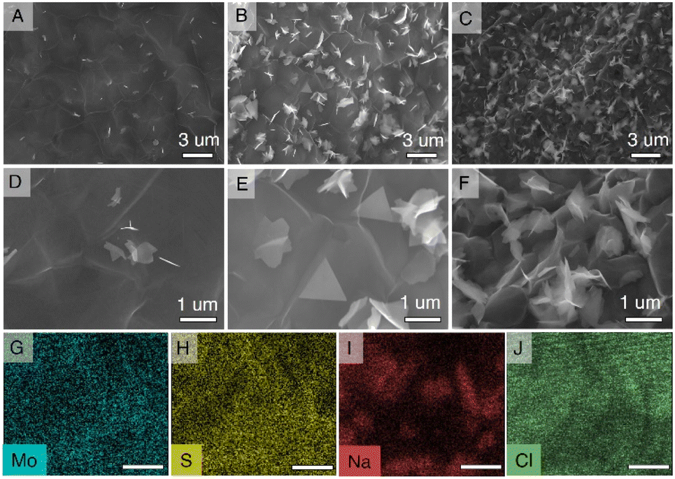 | ||
| Fig. 2 SEM images and elemental analysis of as-grown MoS2@NaCl. The SEM images of MoS2@NaCl after the growth time of (A) 3 min, (B) 5 min, and (C) 10 min, with their magnified view in D–F, and (G–J) the EDS of MoS2@NaCl after 5 min of growth time (scale bar = 2 μm). | ||
The synthesized MoS2@NaCl was then dissolved in water, and the pristine few-layer MoS2 2D nanosheets were obtained via a vacuum filtration technique. The pristine MoS2 was selected as an active material for the LiB anode. In the next part, a sandwich heterostructure of MoS2 2D nanosheets with 0D Si nanoparticles (MoS2@Si) was prepared via vacuum filtration as illustrated in the schematic in Fig. 3A. The main purpose of fabricating the sandwich structure is to trap Si particles in between 2D nanosheets to avoid its volume expansion during lithiation/delithiation and to create void spaces between the 2D nanosheets for better diffusion of Li+. The structure can be seen in the SEM images of the prepared MoS2@Si heterostructure electrode in Fig. 3B–D together with its EDS mapping in Fig. 3E–G which clearly shows the presence of Si and MoS2.
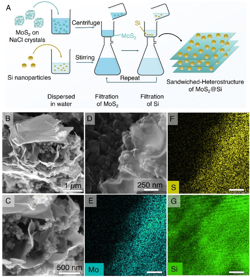 | ||
| Fig. 3 Preparation and analysis of the MoS2@Si heterostructure composite. (A) The schematic illustrates the preparation method of the heterostructure through layer-by-layer addition of MoS2 and Si via vacuum filtration. (B–D) The SEM and (E–G) EDS images of the MoS2@Si heterostructure depict various elements in the composite structure. | ||
Raman, XPS, and porosity analyses were conducted on the obtained MoS2@Si heterostructure samples. The Raman results in Fig. 4A show three peaks at 381.22 cm−1, 407.5 cm−1, and 518.56 cm−1 ascribed to E2g1 and A1g of MoS2 and Si, respectively.33 Moreover, the XPS spectra in Fig. 4B reveal the presence of Mo, S, and Si elements in the MoS2@Si composite. The two Mo 3d peaks at 229.04 eV and 232.18 eV correspond to the Mo 3d5/2 and Mo 3d3/2 (Fig. 4C), validating the presence of Mo4+ in MoS2 and the S 2s peak is observed at 226.35 eV.33,34 The S2− 2p3/2 and S2− 2p1/2 peaks of MoS2 are centered at 162.2 eV and 163.4 eV (Fig. 4D), respectively.35 The Si 2p peak is observed at ∼99.5 eV (Fig. 4E) assigned to the Si bonding in the MoS2@Si, whereas a native oxide layer (SiO2) is detected at 103.9 eV in the Si 2p region, which describes the oxidization of the pure Si to form SiO2.12,36 The pore structures of pristine Si, MoS2, and MoS2@Si were also investigated with the help of the nitrogen adsorption and desorption isotherms (Fig. 4F). From the isotherms, the obtained Brunauer–Emmett–Teller (BET) specific surface area of MoS2@Si (45 m2 g−1) was higher than that of Si (33 m2 g−1) and MoS2 (13 m2 g−1). The large specific surface area obtained for MoS2@Si is mainly due to some MoS2 isolated nanosheets at the edges of the MoS2@Si as observed in the SEM images in Fig. 3. The pore size distribution based on the Barrett–Joyner–Halenda (BJH) method is also shown in Fig. S5.† The average diameter of pores decreases when the Si is sandwiched between MoS2 nanosheets confirming a well-made sandwich composite. These can offer a greater number of active sites which is beneficial for ion storage if such a structure is used as a battery electrode.
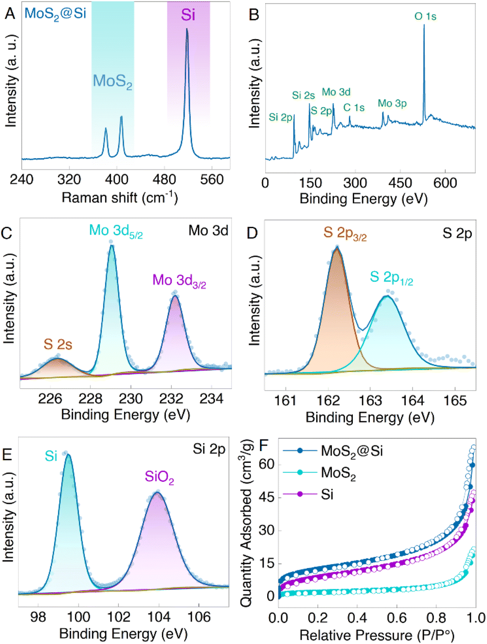 | ||
| Fig. 4 Characterization of the prepared MoS2@Si heterostructure samples. (A) Raman spectra depicting the presence of both MoS2 and Si in the sample. (B) Wide scan XPS and its high resolution fitted (C) Mo 3d, (D) S 2p, and (E) Si 2p core level XPS spectra. (F) Nitrogen adsorption and desorption isotherms of MoS2@Si heterostructure, MoS2, and Si samples obtained at 77 K. | ||
Electrochemical performance
Next, MoS2@Si and MoS2 nanosheets were used as anodes to prepare LiBs in a half-cell configuration (Fig. S6†). The cyclic voltammetry (CV) and long-term galvanostatic charge/discharge (GCD) cyclic measurements were conducted to understand the electrochemical properties and the possible reaction mechanisms. Fig. 5A and B show the CV curves of the MoS2@Si and MoS2 cells measured in a potential window between 0.01 and 3 V at a scan rate of 0.1 mV s−1. Upon the first discharge, the MoS2@Si electrode depicts cathodic peaks at ∼0.01, ∼0.4, and 0.9 V. The broad peak at 0.9 V is associated with the lithiation of MoS2, where Li-ions intercalate into MoS2 nanosheets to form LixMoS2, and it shifts to 1.1 V in the subsequent cycles. This is followed by the conversion reaction at ∼0.4 V, where the reduction of LixMoS2 to Mo metal and Li2S takes place.37,38 The irreversible peaks in the first cycle are due to the solid electrolyte interphase (SEI) formation in the initial lithiation process.39 The sharp peak at ∼0.01 V is a typical Si peak caused by the conversion of Si to the LixSi alloy (Fig. S7A†).40 In the subsequent cycles, the reversible reduction peak 1.8 V is associated with the reduction of S atoms and is predominant in the pristine MoS2 CV curve in Fig. 5B. Similarly, during charging, the prominent anodic peak at 2.3 V and a weak peak at 1.6 V are related to the oxidation of Li2S and metallic Mo to S and the MoS2,41 respectively, which is not present in the Si CV curve in Fig. S7A.† This reversible lithium–sulfur reaction contributes to the Li-ion storage capacity of MoS2.42 The sharp anodic peaks at ∼0.5 V are associated with the delithiation process of the LixSi alloy which is very prominent in the Si CV curves.43,44 The shape of the CV curve and the oxidation/reduction peaks in the latter cycles are almost overlapped with a slight increase in the redox peak area which can reflect the good electrochemical stability and the activation process of the electrode.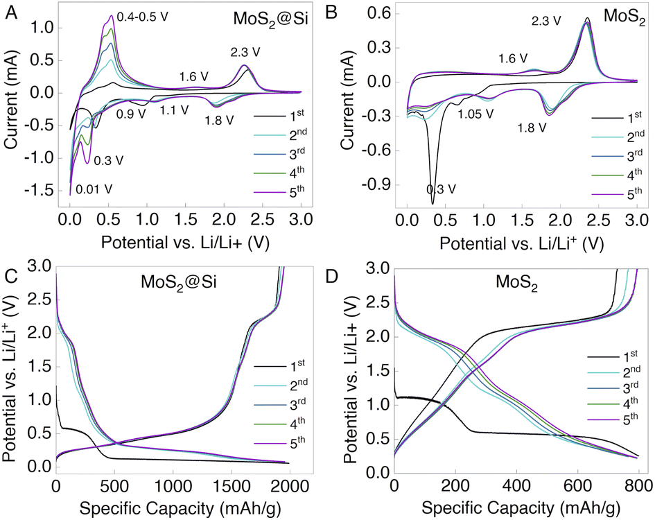 | ||
| Fig. 5 The electrochemical results. (A) CV curves of MoS2@Si and (B) MoS2 at a scan rate of 0.1 mV s−1 within the potential window of 0.01–3.0 V. GCD profiles of the initial five cycles of (C) MoS2@Si and (D) MoS2 at 100 mA g−1. | ||
Furthermore, the GCD test was performed at a current density of 100 mA h g−1 in the voltage window of 0.01–3.0 V for MoS2@Si and MoS2. The voltage profiles of the first five cycles of MoS2@Si and MoS2 are shown in Fig. 5C and D and for Si in Fig. S7B.† Commonly, the discharge capacity between 0.01 V and 3 V is considered to be able to compare with similar values obtained in the literature. However, the practical range lies between 0.01 and 0.5 V, at which the anode potential does not deviate from zero above 0.5 V.45 Whereas, for MoS2@Si, the discharge capacity remains very high, above 1500 mA h g−1, with very good capacity retention and cycle life (Fig. 5C). The three plateaus in the MoS2@Si discharge profile are observed at ∼0.9 V, ∼0.4 V, and ∼0.01 V, describing the combined plateaus of MoS2 and Si electrodes. Thus, the corresponding charge plateaus are consistent with those of cathodic and anodic peaks in cyclic voltammetry (Fig. 5A). The trends of the charge/discharge profiles of the second, third, fourth, and fifth cycles gradually become stable, which further demonstrates that the MoS2@Si electrode has excellent stability.
For the practical applications of LiBs, it is essential for an electrode to have an excellent reversible rate performance. The rate capability of both MoS2 and MoS2@Si electrodes was measured, ranging from low to high current densities, i.e., 100, 200, 300, 500, and 1000 mA g−1, as illustrated in Fig. 6A. The synthesized MoS2 nanosheets demonstrated an exceptional specific capacity of 890 mA h g−1 at 100 mA g−1, which gradually decreased with increasing current density to 508 mA h g−1 at 1000 mA g−1. When the current density increased back to 100 mA g−1, the specific capacity reached up to 911 mA h g−1 with a coulombic efficiency of 98% and remained stable for 20 cycles which proves that the MoS2 2D nanosheets had remarkable rate performance. For MoS2@Si, the capacity at 100 mA g−1 was 2331 mA h g−1 and dropped to 625 mA h g−1 at a very high current density of 1000 mA g−1. On returning to 100 mA g−1, its specific capacity and coulombic efficiency reached 1707 mA h g−1 and 98%, respectively. The charge/discharge capacities of MoS2 and MoS2@Si at different current densities are given in Table S1.†
 | ||
| Fig. 6 (A) The rate capability of MoS2@Si and MoS2 at 100, 200, 300, 500, and 1000 mA g−1. (B–C) Cyclic behaviors of MoS2@Si, MoS2, and Si at 100 and 500 mA g−1. (D–F) Cross-sectional SEM images of delithiated electrodes after 500 cycles at 500 mA g−1 (scale bar = 20 μm). | ||
The long-term cycling performance of the electrodes was evaluated at 100 and 500 mA g−1, as shown in Fig. 6B and C. The initial discharge capacities of MoS2, MoS2@Si, and Si electrodes at 100 mA g−1 were 1812, 2825, and 3466 mA h g−1, respectively. The discharge capacities dropped in the second cycle to 739, 2033, and 2551 mA h g−1, respectively (Fig. 6B). Further, the coulombic efficiencies of MoS2 and MoS2@Si anodes were 70% and 73% in the first cycle. The low initial coulombic efficiency can be due to the SEI formation which decomposes the electrolyte in the first cycle. To reduce the initial capacity loss and increase the initial coulombic efficiency of Si, some strategies including optimization of electrolyte, prelithiation, structure and morphology design, defects engineering, and binder optimization can be utilized.46–49 Nevertheless, in our half cells, the coulombic efficiencies increased to 91% and 96% in the second cycle. MoS2 and MoS2@Si electrodes showed excellent reversible cycling performance maintaining the specific capacity of 624 and 1223 mA h g−1 after 300 cycles with 99% coulombic efficiency. The improved capacity, cycling stability, and high coulombic efficiency are due to the unique structure of MoS2@Si. Though the Si electrode shows a higher capacity at low current density but becomes unstable as the capacity drops to 959 mA h g−1 at ∼300 cycles.
In Fig. 6C, MoS2@Si showed excellent capacity retention of ∼60% after 500 cycles at a high current density of 500 mA g−1 with a coulombic efficiency of 99%. However, we note that its specific capacity at a low current density of 100 mA g−1 was lower than that of pure Si, up to ∼260 cycles. We believe this is related to the unique structure of few-layered MoS2 2D nanosheets sandwiching the Si nanoparticles in the heterostructure. In all experiments, we observed that Si always has a higher capacity in the initial cycles than MoS2@Si. However, the capacity of Si drops gradually below that of MoS2@Si due to increased instability. At a high current density, MoS2@Si performs better even at earlier cycles as MoS2 is able to mitigate Si volume expansion and particle pulverization, considered as the synergistic interaction between 2D sheets and Si.50–52 At low current density, the volume expansion of Si becomes less significant and it can last for ∼260 cycles before its capacity drops below MoS2@Si due to the low current density-driven lithiation and delithiation, in which we expect a less adverse expansion of Si electrodes and tampering of the electrode structure. It is worth noting that pristine Si in all our experiments showed a higher specific capacity than the composite, albeit with poor stability. The composite despite lower specific capacity (mainly due to the presence of MoS2, with low specific capacity) in comparison to pristine Si consistently showed reliable stability even at a higher density which we attributed to the improved volume expansion. It is well known that the stresses caused by the repetitive volume expansion and contraction of Si can lead to cracking and pulverization of the electrode resulting in capacity loss.53 Hence, it can be concluded that MoS2 acts as a buffer as it sandwiches the Si nanoparticles between its nanosheets, limiting the extent of repetitive volume expansion and contributing to improved cycling stability.
To understand the role of MoS2 nanosheets in the lithiation/delithiation, the volume change of the anodes after a certain number of cycles was examined. We further analyzed the SEM images of the cross-section of MoS2@Si, MoS2, and Si electrodes at a fully delithiated state after 500 cycles at 500 mA g−1 as given in Fig. 6D–F in comparison to the initial measurements prior to cycling in Fig. S8.† It can be clearly observed that the thickness of the Si electrode expanded from 10 μm to 53 μm after 500 cycles which is ∼430% volume expansion. In comparison, the thickness of MoS2@Si increased from 19 μm to 32 μm after 500 cycles with around 68% of volume expansion. Therefore, introducing MoS2 nanosheets into the overall electrode significantly reduces the volume expansion (Fig. 7A).51,52,54,55 This performance is superior compared to past reported results given in Table S2.† The surface morphology of the MoS2@Si and Si anodes can be observed from the SEM images before and after 500 cycles of lithiation/delithiation in Fig. 7B and C and S9.† For the MoS2@Si electrode, Si particles almost maintained their structure (Fig. 7B) with few cracks after 500 cycles (Fig. S9A†). However, the round-like crystalline Si particles in the Si electrode transformed into larger irregular shapes after lithiation/delithiation cycles (Fig. 7C) with various cracks around the electrode (Fig. S9B†). The expansion of Si nanoparticles is limited by the MoS2 nanosheets. The pores within the MoS2 can also accommodate some volume expansion of Si. In addition, the presence of MoS2 2D nanosheets is observed to improve the formation of the SEI layer (Fig. S10†). Also, our previous molecular dynamics simulation indicates that wrapping Si particles with 2D nanosheets can reduce mechanical stresses during cycling.56 As discussed, MoS2 is an active material and can achieve stable cycle performance (Fig. 6 A–C). This proves that the fabrication of the heterostructure with MoS2@Si is responsible for the excellent performance observed here.
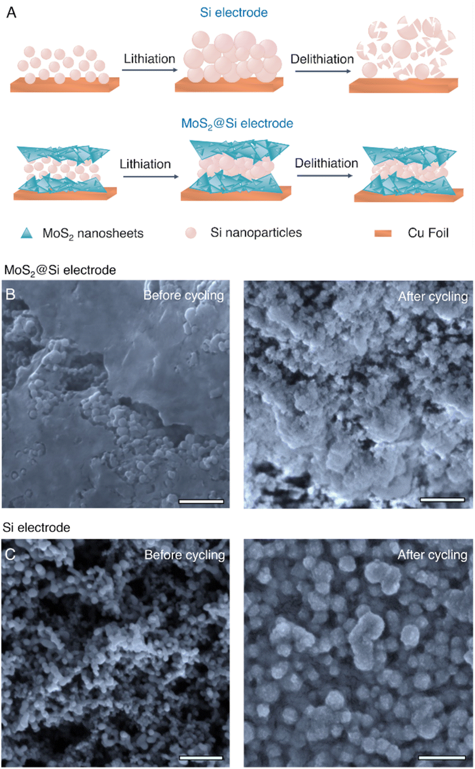 | ||
| Fig. 7 (A) The schematic showing Si nanoparticles sandwiched between MoS2 nanosheets improving the volume expansion of the MoS2@Si electrode. SEM images of the (B) MoS2@Si and (C) Si electrodes before and after 500 cycles. The scale bar is 500 nm. | ||
To confirm the excellent electrochemical performance of MoS2@Si electrodes, we also analyzed charge transfer and diffusion resistance of the Si, MoS2, and MoS2@Si electrodes from GCD discharge curves for cycles 1, 2, 5, 50, and 500 (Fig. S11†). The charge transfer resistance of the MoS2 and MoS2@Si electrode decreased after the first cycle in the subsequent second cycle from 266 Ω to 246 Ω and 1084 Ω to 57 Ω, respectively, owing to the transformation of MoS2 into a metallic high conductive phase and formation of the conductive SEI layer during the first discharge process.57 The charge-transfer resistance of these electrodes continued to decrease to 240 Ω and 55 Ω in the 5th cycle before stabilizing to the low resistance of 44 Ω and 81 Ω in the 50th cycle and finally increasing to 158 Ω and 126 Ω at 500th cycle, which was very low as compared to the first cycle. However, for Si, the charge transfer resistance for the first cycle started low at 120 Ω but ended at 185 Ω, which we ascribe to be due to the electrode failure and cracks after 500 cycles.
Conclusion
We synthesized MoS2 2D nanosheets on a water-soluble NaCl substrate. This enabled us to get few-layer and isolated 2D sheets of MoS2 which was utilized to prepare a heterostructure with Si nanoparticles in a layer-by-layer assembly. To investigate the working mechanism, the pristine MoS2 and MoS2@Si sandwich structures were used as the anodes for Li-ion batteries. The assembled cells demonstrated remarkable rate capability, i.e., 890 and 2331 mA h g−1 at 100 mA g−1 for the MoS2 and MoS2@Si anodes, respectively, with the coulombic efficiency of above 98%. The long-term cycling stability of the heterostructure MoS2@Si electrode was observed to outperform that of MoS2 and Si to a great extent. Specifically, after 500 cycles, the MoS2@Si showed excellent cycling stability with capacity retention of 60% compared to 21% from MoS2 and 0.3% from pristine Si at a high current density of 500 mA g−1. A significant reduction in volume expansion is observed in the MoS2@Si anode (68%) compared to pristine Si (about 430%). The layered MoS2 nanosheets in the heterostructure can accommodate the volume expansion of Si particles and contribute to excellent electrochemical performance. The approach to synthesizing MoS2 2D nanosheets and their utilization in a sandwich heterostructure add advantage to the already existing promising application of MoS2 for energy storage applications.Author contributions
The manuscript was written through the contributions of all authors. I. Marriam performed most of the experiments, collected and analyzed the data, wrote the first draft, and took responsibility for this article overall. C. Yan and A. Du supervised the experiments and writing of the article. M. Tebyetekerwa edited the second draft of the article and provided insights into the growth and Raman spectroscopy of MoS2. N. Motta provided the CVD equipment and supervised the synthesis of MoS2. J. A. Alarco provided the glovebox and supervised the battery assembling process. H. Chen, H. Chathuranga, Z. J. He, and J. C. Zheng supported the development of some experiments. All the authors discussed the contents of the manuscript prior to submission and revised the final draft of the manuscript. All authors have approved the final version of the manuscript.Conflicts of interest
The authors declare that they have no known competing financial interests or personal relationships that could have appeared to influence the work reported in this paper.Acknowledgements
The authors acknowledge the support from the Central Analytical Research Facility (CARF) and Centre for Materials Science at Queensland University of Technology (QUT). The PhD scholarship (QUTPRA) from Queensland University of Technology, Brisbane, Australia, and the financial support from an ARC Discovery Project (DP180102003) are highly appreciated.References
- X. Y. Zhang, L. L. Hou, A. Ciesielski and P. Samori, Adv. Energy Mater., 2016, 6, 1600671 CrossRef.
- L. X. Lin, J. Chen, D. Z. Liu, X. F. Li, G. G. Wallace and S. W. Zhang, Adv. Energy Mater., 2020, 10, 2002621 CrossRef CAS.
- J. Zhou, J. Lin, X. Huang, Y. Zhou, Y. Chen, J. Xia, H. Wang, Y. Xie, H. Yu, J. Lei, D. Wu, F. Liu, Q. Fu, Q. Zeng, C. H. Hsu, C. Yang, L. Lu, T. Yu, Z. Shen, H. Lin, B. I. Yakobson, Q. Liu, K. Suenaga, G. Liu and Z. Liu, Nature, 2018, 556, 355–359 CrossRef CAS PubMed.
- I. Marriam, M. Tebyetekerwa, Z. Xu, H. Chathuranga, S. Chen, H. Chen, J.-C. Zheng, A. Du and C. Yan, Energy Storage Mater., 2021, 43, 62–84 CrossRef.
- I. Marriam, Y. Wang and M. Tebyetekerwa, Energy Storage Mater., 2020, 33, 336–359 CrossRef.
- U. Sharma, S. Karazhanov, R. Jose and S. Das, J. Mater. Chem. A, 2022, 10, 8626–8655 RSC.
- E. Pomerantseva, F. Bonaccorso, X. Feng, Y. Cui and Y. Gogotsi, Science, 2019, 366, eaan8285 CrossRef CAS PubMed.
- F. Bonaccorso, L. Colombo, G. Yu, M. Stoller, V. Tozzini, A. C. Ferrari, R. S. Ruoff and V. Pellegrini, Science, 2015, 347, 1246501 CrossRef PubMed.
- B. Simon, S. Flandrois, K. Guerin, A. Fevrier-Bouvier, I. Teulat and P. Biensan, J. Power Sources, 1999, 81, 312–316 CrossRef.
- D. Aurbach, B. Markovsky, I. Weissman, E. Levi and Y. Ein-Eli, Electrochim. Acta, 1999, 45, 67–86 CrossRef CAS.
- P. Novák, F. Joho, M. Lanz, B. Rykart, J.-C. Panitz, D. Alliata, R. Kötz and O. Haas, J. Power Sources, 2001, 97–98, 39–46 CrossRef.
- D. H. S. Tan, Y. T. Chen, H. Yang, W. Bao, B. Sreenarayanan, J. M. Doux, W. Li, B. Lu, S. Y. Ham, B. Sayahpour, J. Scharf, E. A. Wu, G. Deysher, H. E. Han, H. J. Hah, H. Jeong, J. B. Lee, Z. Chen and Y. S. Meng, Science, 2021, 373, 1494–1499 CrossRef CAS PubMed.
- M. T. McDowell, S. W. Lee, W. D. Nix and Y. Cui, Adv. Mater., 2013, 25, 4966–4985 CrossRef CAS PubMed.
- C. Y. Du, C. H. Gao, G. P. Yin, M. Chen and L. Wang, Energy Environ. Sci., 2011, 4, 1037–1042 RSC.
- J. Xiao, D. W. Choi, L. Cosimbescu, P. Koech, J. Liu and J. P. Lemmon, Chem. Mater., 2010, 22, 4522–4524 CrossRef CAS.
- C. Q. Feng, J. Ma, H. Li, R. Zeng, Z. P. Guo and H. K. Liu, Mater. Res. Bull., 2009, 44, 1811–1815 CrossRef CAS.
- K. Chang and W. Chen, Chem Commun., 2011, 47, 4252–4254 RSC.
- S. Zhu, C. Wang, H. Shou, P. Zhang, P. Wan, X. Guo, Z. Yu, W. Wang, S. Chen, W. Chu and L. Song, Adv. Mater., 2022, 34, 2108809 CrossRef CAS PubMed.
- H. Hwang, H. Kim and J. Cho, Nano Lett., 2011, 11, 4826–4830 CrossRef CAS PubMed.
- U. V. Kawade, A. A. Ambalkar, R. P. Panmand, R. S. Kalubarme, S. R. Kadam, S. D. Naik, M. V. Kulkarni and B. B. Kale, Mater. Chem. Front., 2019, 3, 587–596 RSC.
- K. Kang, S. Xie, L. Huang, Y. Han, P. Y. Huang, K. F. Mak, C. J. Kim, D. Muller and J. Park, Nature, 2015, 520, 656–660 CrossRef CAS PubMed.
- P. Yang, X. Zou, Z. Zhang, M. Hong, J. Shi, S. Chen, J. Shu, L. Zhao, S. Jiang, X. Zhou, Y. Huan, C. Xie, P. Gao, Q. Chen, Q. Zhang, Z. Liu and Y. Zhang, Nat. Commun., 2018, 9, 979 CrossRef PubMed.
- H. Yu, M. Liao, W. Zhao, G. Liu, X. J. Zhou, Z. Wei, X. Xu, K. Liu, Z. Hu, K. Deng, S. Zhou, J. A. Shi, L. Gu, C. Shen, T. Zhang, L. Du, L. Xie, J. Zhu, W. Chen, R. Yang, D. Shi and G. Zhang, ACS Nano, 2017, 11, 12001–12007 CrossRef CAS PubMed.
- H. R. Jin, Z. M. Hu, T. Q. Li, L. Huang, J. Wan, G. B. Xue and J. Zhou, Adv. Funct. Mater., 2019, 29, 1900649 CrossRef.
- M. Tebyetekerwa, J. Zhang, S. E. Saji, A. A. Wibowo, S. Rahman, T. N. Truong, Y. R. Lu, Z. Y. Yin, D. Macdonald and H. T. Nguyen, Cell Rep. Phys. Sci., 2021, 2, 100509 CrossRef CAS.
- L. J. Zhu, P. F. Yang, Y. H. Huan, S. Y. Pan, Z. Q. Zhang, F. F. Cui, Y. P. Shi, S. L. Jiang, C. Y. Xie, M. Hong, J. T. Fu, J. Y. Hu and Y. F. Zhang, Nano Res., 2020, 13, 3098–3104 CrossRef CAS.
- I. Marriam, M. Tebyetekerwa, H. Chathuranga, S. Yang and C. Yan, in Smart and Flexible Energy Devices, CRC Press, 2022, pp. 397–415 Search PubMed.
- S. Ding, D. Zhang, J. S. Chen and X. W. Lou, Nanoscale, 2012, 4, 95–98 RSC.
- M. Tebyetekerwa, J. Zhang, K. Liang, T. Duong, G. P. Neupane, L. Zhang, B. Liu, T. N. Truong, R. Basnet, X. Qiao, Z. Yin, Y. Lu, D. Macdonald and H. T. Nguyen, Adv. Mater., 2019, 31, e1900522 CrossRef PubMed.
- A. P. Nayak, T. Pandey, D. Voiry, J. Liu, S. T. Moran, A. Sharma, C. Tan, C. H. Chen, L. J. Li, M. Chhowalla, J. F. Lin, A. K. Singh and D. Akinwande, Nano Lett., 2015, 15, 346–353 CrossRef CAS PubMed.
- J. Zhang, M. Tebyetekerwa and H. T. Nguyen, J. Colloid Interface Sci., 2022, 611, 432–440 CrossRef CAS PubMed.
- F. Chen and W. T. Su, CrystEngComm, 2018, 20, 4823–4830 RSC.
- X. L. Zhang, L. W. Huang, P. Zeng, L. Wu, Q. Q. Shen, Z. X. Gao and Y. G. Chen, Chem. Eng. J., 2019, 357, 625–632 CrossRef CAS.
- W. N. Ren, H. F. Zhang, C. Guan and C. W. Cheng, Adv. Funct. Mater., 2017, 27, 1702116 CrossRef.
- J. Liu, Z. Jia, W. Zhou, X. Liu, C. Zhang, B. Xu and G. Wu, Chem. Eng. J., 2022, 429, 132253 CrossRef CAS.
- J. Sung, N. Kim, J. Ma, J. H. Lee, S. H. Joo, T. Lee, S. Chae, M. Yoon, Y. Lee, J. Hwang, S. K. Kwak and J. Cho, Nat. Energy, 2021, 6, 1164–1175 CrossRef.
- X. B. Ye, C. H. Gan, L. Q. Huang, Y. W. Qiu, Y. Xu, L. Y. Huang and X. T. Luo, ChemElectroChem, 2021, 8, 1270–1279 CrossRef CAS.
- Z. Liu, K. Wang, G. Huang, S. Yu, X. Li, N. Li and K. Yu, Nanoscale, 2022, 14, 8621–8627 RSC.
- J. Wang, J. Liu, D. Chao, J. Yan, J. Lin and Z. X. Shen, Adv. Mater., 2014, 26, 7162–7169 CrossRef CAS PubMed.
- C. Gan, C. Zhang, W. Wen, Y. Liu, J. Chen, Q. Xie and X. Luo, ACS Appl. Mater. Interfaces, 2019, 11, 35809–35819 CrossRef CAS PubMed.
- X. Liu, P. Mei, Y. Dou, R. Luo, Y. Yamauchi and Y. Yang, J. Mater. Chem. A, 2021, 9, 13001–13007 RSC.
- H. Lu, K. Tian, L. Bu, X. Huang, X. Li, Y. Zhao, F. Wang, J. Bai, L. Gao and J. Zhao, J. Energy Chem., 2021, 55, 449–458 CrossRef CAS.
- Y. Chen, J. Li, G. Yue and X. Luo, Nanomicro Lett., 2017, 9, 32 Search PubMed.
- J. X. Wu, X. Y. Qin, C. Miao, Y. B. He, G. M. Liang, D. Zhou, M. Liu, C. P. Han, B. H. Li and F. Y. Kang, Carbon, 2016, 98, 582–591 CrossRef CAS.
- M. Gao, B. Liu, X. Zhang, Y. Zhang, X. Li and G. Han, J. Alloys Compd., 2022, 894, 162550 CrossRef CAS.
- H. Zhang, K. Liu, Y. Liu, Z. Lang, W. He, L. Ma, J. Man, G. Jia, J. Cui and J. Sun, J. Power Sources, 2020, 447, 227400 CrossRef CAS.
- H. He, D. Sun, Y. Tang, H. Wang and M. Shao, Energy Storage Mater., 2019, 23, 233–251 CrossRef.
- M. Tebyetekerwa, T. T. Duignan, Z. Xu and X. Song Zhao, Adv. Energy Mater., 2022, 12, 2202450 CrossRef CAS.
- F. Xie, Z. Xu, Z. Y. Guo, A. C. S. Jensen, J. Y. Feng, H. Luo, F. X. Ding, Y. X. Lu, Y. S. Hu and M. M. Titirici, Carbon Energy, 2022, 4, 914–923 CrossRef CAS.
- M. Ko, S. Chae and J. Cho, ChemElectroChem, 2015, 2, 1645–1651 CrossRef CAS PubMed.
- H. Liu, W. Yang, S. Che, Y. Li, C. Xu, X. Wang, G. Ma, G. Huang and Y. Li, Carbon, 2022, 196, 633–638 CrossRef CAS.
- Y. Liu, W. Sun, X. Lan, R. Hu, J. Cui, J. Liu, J. Liu, Y. Zhang and M. Zhu, ACS Appl. Mater. Interfaces, 2019, 11, 38727–38736 CrossRef CAS PubMed.
- B. Liang, Y. P. Liu and Y. H. Xu, J. Power Sources, 2014, 267, 469–490 CrossRef CAS.
- T. Chen, J. Hu, L. Zhang, J. Pan, Y. Liu and Y.-T. Cheng, J. Power Sources, 2017, 362, 236–242 CrossRef CAS.
- Z.-L. Xu, Y. Gang, M. A. Garakani, S. Abouali, J.-Q. Huang and J.-K. Kim, J. Mater. Chem. A, 2016, 4, 6098–6106 RSC.
- K. C. Wasalathilake, S. N. S. Hapuarachchi, Y. B. Zhao, J. F. S. Fernando, H. Chen, J. Y. Nerkar, D. Golberg, S. Q. Zhang and C. Yan, ACS Appl. Energy Mater., 2020, 3, 521–531 CrossRef CAS.
- X. Fan, M. Tebyetekerwa, Y. Wu, R. R. Gaddam and X. S. Zhao, Energy mater. adv., 2022, 2022 Search PubMed.
Footnote |
| † Electronic supplementary information (ESI) available. See DOI: https://doi.org/10.1039/d2ta08886j |
| This journal is © The Royal Society of Chemistry 2023 |