
 Open Access Article
 This Open Access Article is licensed under a
 Creative Commons Attribution 3.0 Unported Licence
2D material-based sensing devices: an update
Jahan Zeb
Hassan†
 a,
Ali
Raza†
*b,
Zaheer Ud
Din Babar†
bc,
Usman
Qumar
a,
Ngeywo Tolbert
Kaner
d and
Antonio
Cassinese
b
a,
Ali
Raza†
*b,
Zaheer Ud
Din Babar†
bc,
Usman
Qumar
a,
Ngeywo Tolbert
Kaner
d and
Antonio
Cassinese
b
aDepartment of Physics, Riphah Institute of Computing and Applied Sciences (RICAS), Riphah International University, 14 Ali Road, Lahore, Pakistan
bDepartment of Physics “Ettore Pancini”, University of Naples Federico II, Piazzale Tecchio, 80, 80125 Naples, Italy. E-mail: ali.raza@unina.it
cScuola Superiore Meridionale (SSM), University of Naples Federico II, Largo S. Marcellino, 10, 80138, Italy
dSchool of Physics, Harbin Institute of Technology, Harbin 150001, China
First published on 6th March 2023
Abstract
In recent decades, two-dimensional materials have attracted significant attention due to their unique chemical and physical properties, which are useful for various applications. In addition to optoelectronic devices and energy harvesting and storage, 2D materials are used in many sensing applications. Two-dimensional structures have numerous attributes, such as high surface sensitivity, excellent biocompatibility, and high elasticity, making them effective as sensing devices. In this review, we aim to provide an update on the recent developments in the field of sensors fabricated using atomically thin 2D materials. A survey of different types of sensors is presented, including gas, electrochemical, biomedical, and health sensors, together with recent findings on their real-world applications. Furthermore, human body temperature monitoring, electrography, sweat detection, respiratory gas, and saliva sensors are also reviewed to assess current trends toward human chemical signal detection. Given that 2D materials encompass a vast array of novel materials, we highlight the contemporary trend in the applications of 2D materials and suggest the exciting future of the 2D family. By thoroughly addressing the fundamental aspects, recent developments, and associated challenges, our recommendation in terms of future challenges and prospects will pave the way for readers.
 Jahan Zeb Hassan | Jahan Zeb Hassan obtained his M. Sc. degree in physics from the University of Gujrat, Pakistan, in 2017 and M. Phil from Riphah International University, Islamabad, in 2020. Hassan completed his research work in Solar Cell Applications Lab at GCU Lahore. He later worked as Research Assistant in the same lab to synthesize 2D materials for energy harvesting applications. Hassan worked as Lecturer (visiting) in Physics at GC University Faisalabad (Chanab College Sub Campus). Currently, he is a Member of American Physical Society with research direction of designing layered materials for sensing and storage devices. |
 Ali Raza | Ali Raza obtained his BS (Physics) degree from the University of Gujrat (Pakistan) in 2016 and Master's in Material Physics from Riphah International University, Islamabad, in 2019. Raza completed his M. Phil research in the Solar Cell Applications Lab at GCU Lahore and later worked as Research Associate in the same lab in the field of catalytic and energy harvesting applications of pure and engineered 2D materials (TMDCs, Graphene, h-BN, and MXenes). Later, he served as Lecturer (Research) at the Department of Physics, University of Sialkot. Currently, he is a doctoral fellow at the Department of Physics “Ettore Pancini”, University of Naples Federico II, Italy. His current research directions are the fabrication of functional 2D materials for sensing and green energy-harvesting applications. |
 Zaheer Ud Din Babar | Zaheer Ud Din Babar earned his MS in Physics from National University of Sciences and Technology (NUST), Pakistan, in 2019. During his Master's research, he investigated the magnetic properties of Nb2C MXene and reported its superconductive nature. Currently, Babar is a PhD Scholar in “Mathematical and Physical Sciences for Advanced Materials and Technologies (MPHS)” at Scuola Superiore Meridionale (SSM) and pursuing his research project at the Department of Physics “E. Pancini”, University of Naples Federico II, Italy. His current research interest includes the synthesis of 2D-MXenes and their nanocomposites with gold and magnetic nanoparticles for (bio)sensing applications. |
 Usman Qumar | Usman Qumar obtained his M.Sc. in Physics from the University of Gujrat (Pakistan) in 2017 and his M. Phil (Physics) from Riphah International University, Islamabad in 2020. Qumar performed his M. Phil research in the Solar Cell Applications Lab at GCU Lahore and later worked as a Research Assistant at the department of Physics Riphah International University Lahore Campus. Currently, he is working as a lecturer (visiting) in the Physics department at University of Gujrat. His current research areas are the fabrication of 2D materials for energy harvesting (chemical and mechanical) applications. Qumar is a member of international journal of Pakistan Science Society and American Physical Society (APS). |
 Ngeywo Tolbert Kane | Ngeywo Tolbert Kane received his Bachelor of Education (Science) degree with honors from Moi University, Eldoret (Kenya), in 2006. He completed his Master of Science in Physics (2014–2016) at the University of Eldoret. Currently, he is a final year PhD scholar in Physics at the Harbin Institute of Technology (HIT, China). His work is on nonlinear optics in emerging two-dimensional ferroelectrics, sensing, and electronic devices under the mentorship of Professor Yongyuan Jiang. |
 Antonio Cassinese | Antonio Cassinese is a Professor of Experimental Physics of Matter at the Department of Physics, University of Naples Federico II. He received PhD in Physics at the same University in 1996, spending a period as Associated Research at the CERN Laboratories and the University of Wuppertal, Germany, under Marie Curie individual fellowship. From 2002 to 2014, he was a permanent Researcher at the University of Naples Federico II. The scientific activity was carried out to investigate the electrical properties of superconductors, oxides, organic (polymer), and inorganic hybrids materials to understand physical fundamental aspects and possible practical applications in the electronic fields. He produced more than 200 research publications in peer-reviewed journals. Currently, Cassinese is running a research group with activities belonging to the fabrication of 2D and organic materials for electronic devices and manipulation of spin with high Q microwave cavities for quantum sensing applications. |
1 Introduction
Over the past two decades, research on 2D materials has witnessed a remarkable increase after Geim and Novoselov's ground-breaking experiments in 2004 and the discovery of graphene.1 Since then, based on its exceptional physical characteristics, graphene has become prominent in various research areas of nanoscience and condensed matter physics/chemistry, significantly contributing to a wide range of interdisciplinary fields. Accordingly, the large-scale preparation of graphene-based materials has gained extensive consideration, leading to cutting-edge research and innovative technologies. Concurrently, various enterprises and manufacturers have contributed to the industrialization of graphene. Furthermore, due to its physicochemical characteristics and wide spectrum of applications, interest in graphene has shifted beyond academics to scientific research and industry.2 However, its susceptible nature to oxidative environments, evidence of certain toxicity, and ideal conductive characteristics, which make it unswitchable, are the primary shortcomings of this wonder material.3 Thus, the initial enthusiasm created by the “graphene rush” has shifted to exploring more stable and atomically thin materials. Examples of this type of layered materials are boron nitride,4 recently discovered class of materials (e.g., MXenes) composed of transition metal carbonitrides, nitrides, and carbides,5 semiconducting transition metal dichalcogenides (TMDCs),6 and phosphorene.7–9Table 1 presents some of the principal advancements and recent discoveries in the field of 2D materials. Several pioneering discoveries regarding liquid phase exfoliation are also discussed, including biomedical and sensing applications. The wide range of physical and chemical properties of 2D materials shows significant possibilities for applied research, given that their properties are dependent on their dimensionality.10 Further, various optoelectronic characteristics can be realized, ranging from the extraordinary semi-metal conductivity of graphene11 to the semiconducting properties of certain TMDCs.12 These TMDCs provide a tunable bandgap energy with easy conversion from bulk materials (indirect-form) to single-layered materials (direct-form).13 These properties result in distinct photoluminescence (PL) characteristics, thus permitting diverse applications, e.g., electroluminescent devices,14 photodetectors,15 luminescent probes,16 and transistors.17 Furthermore, chemical functionalization can offer desirable optoelectronic properties in the above-mentioned 2D materials. For example, due to their large surface/volume ratio, their demand has increased in the field of sensing and broadened their application area from the quantitative determination of heavy metal ions (e.g., Cd2+, Pb2+, As3+, and Hg2+),18 gases (e.g., NH3),19 and ultrasensitive detection of essential biomolecules (e.g., DNA and proteins)20 to single molecule detection21 and beyond.22 Notably, 2D material-based sensors do not possess intrinsic properties to interact with target molecules selectively. Thus, it is possible to manipulate the interaction between 2D nanosheets and molecules/ions by modifying their inherent properties. Chemical adsorption (i.e., chemisorption) of interacting substances via covalent bonds on the basal planes of 2D materials provides significant control of their sensing profile. In contrast, physical adsorption (i.e., physisorption) of interacting molecules on the basal planes of 2D materials via non-covalent interactions is preferred in sensing.23 These non-covalent interactions offer high recovery rates and are considered promising for real-time monitoring and rapid onsite analysis. Given that physisorption depends on the nature of the molecules and the interacting surface, it has certain limitations. This involves the ineffective and unstable immobilization of molecules, which can potentially cause false positive and negative results. Primarily, a direct electrical response is desirable for practical applications, where the interaction of analytes with 2D materials generates an enticing optical response, for instance, a variation in PL characteristics offers a variety of opportunities. Graphene and its oxide (GO) are known to be effective fluorescence quenchers compared to organic substances. Hence, Förster resonance energy transfer (FRET) sensors have attracted significant attention in recent years, particularly in biomedical applications. Generally, in biomedical applications, FRET can detect in vitro and in vivo changes and be used to precisely measure nanometer-scale distances.24 This has resulted in the development of nano-biosensors with exceptional selectivity, increased bio-stability, and improved sensitivity. In this regard, single-layer MoS2 nanosheets with superior fluorescence quenching efficiency are a suitable sensing platform for small molecule determination and DNA detection.25 The use of 2D materials in FRET sensors is not limited to energy acceptors. Alternatively, suitable functionalization produces photoluminescent flakes, which act as energy donors, and thus quenched by electron-deficient compounds, e.g., for the detection of trinitrophenol, which is an integral component of intense explosives.26 Recently, 2D materials have been the focus of research for the fabrication of extremely selective and sensitive sensing devices to detect organic vapors, humidity, and hazardous chemicals. These 2D material-based devices are widely used in emission control, environmental monitoring, and diagnosis. In this regard, a broad spectrum of materials has been developed, ranging from carbon materials to metal oxides and various polymers. Certainly, 2D materials should be highlighted owing to their noteworthy features and potential use.27,28 These materials include layered metal oxides, black phosphorus, hexagonal boron nitride (h-BN), pnictogens, TMDCs, and MXenes. Because of their high adsorption capacity and broad surface area, these materials exhibit improved performances for gas sensing. Two configurations of the above-mentioned 2D materials have been utilized in gas sensors, i.e., field-effect transistors (FETs)29 and chemiresistors.30 Because of their ease of attachment, point-of-care sensing, and the ability to construct compact wearable electronic devices, 2D materials have become superior technology for assessing human physiological signals.| Hallmarks in discovery, exfoliations, and sensing applications | |||
|---|---|---|---|
| Material | Timeline | Comments | Ref. |
| Abbreviations: TMCCs = transition metal carbo-chalcogenides (a combination of MXenes and TMDCs at the atomic level), MBenes = transition metal borides, NIR = near-infrared.a TM2X2C layers were intercalated electrochemically with lithium and subsequently sonicated in water.b Synthesis of 2D-CrB (MBene) by immersing Cr2AlB2 (MAB phase) in HCl for 6 h at room temperature.c Ti3AlC2 MAX powder was immersed in 50% HF solution at RT for 2 h.d Immersion and exfoliation of graphite in an organic solvent such as N-methyl-pyrrolidone.e Immersion of MoS2, WS2, and BN in various organic solvents followed by bath sonication and centrifuge. | |||
| TMCCs | 2022 | Discovery and first report of liquid phase exfoliationa | 42 |
| MBenes | 2017 | Discovery of MBenes | 43 |
| 2018 | Liquid phase exfoliationb | 44 | |
| 2021 | In silico study on destabilization of amyloid-β accumulation | 45 | |
| MXenes | 2011 | Liquid phase exfoliationc | 46 |
| 2014 | Ti3C2Tx nanosheets towards H2O2 sensing | 47 | |
| 2017 | Ti3C2Tx nanosheets for photothermal conversion | 48 | |
| Graphene | 2004 | Synthesis of single-layer graphene | 49 |
| 2008 | First report on DNA sensing | 50 | |
| 2008 | Earliest findings on drug delivery for cancer treatment | 51 | |
| 2009 | Liquid-phase exfoliationd | 52 | |
| TMDCs | 1986 | First studies on a single-layer MoS2 | 53 |
| 2011 | Liquid-phase exfoliatione | 54 | |
| 2011 | Detection of NO at room temperature | 55 | |
| 2013 | Earliest study on MoS2 as NIR photothermal agent | 56 | |
They play a vital role in disease diagnosis, regular health assessment, rehabilitation treatment, and preventive medicine.31,32 Currently, in the fabrication of conventional wearable products mainly containing silicon and organic materials, biological compatibility is not an issue. Consequently, researchers are focused on developing multipurpose wearable electronic devices with pertinent features such as light weight, flexibility, and increased performance. These features can enable the development of devices with superior recognition of different types of electrography33 including electromyography, electrooculography, electroencephalography, and electrocardiography, which generate mechanical34,35 and bio-signals in human fluid.36 These signals greatly influence operational indicators for activities and vital signs. As previously indicated, extensive studies on 2D material-based sensing are motivated by their inherent mechanical properties. In addition to continuous fitness tracking and health monitoring of the wearer and their surroundings, these characteristics can be used to create wearable and portable sensing devices, which can significantly impact our society.37 Wearable chemical sensors can perform various tasks, including data acquisition, analytical operations, processing, communication, and safety monitoring. In this case, it is crucial to assess the trends of smart technologies and their possible future activities concerning 2D materials.
Several reviews have been published on 2D materials;24,38–41 however, the current review presents an update on the recent development in the field of sensor devices comprised of atomically thin 2D materials. An investigation on different types of sensors is presented, including gas, electrochemical sensing, biomedical, and healthcare sensors, with recent studies on the active application areas of these materials (see Fig. 1). This study considers different aspects of various sensing applications, including human chemical signal monitoring and personalized healthcare; and also outlines the current challenges and future perspective of these 2D materials.
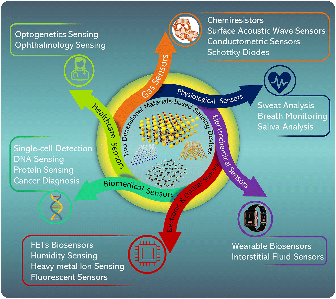 | ||
| Fig. 1 Highlights of 2D materials in various sensing devices. | ||
2 Why 2D materials for sensing?
2D materials have variable thicknesses ranging from a few nanometers to several centimeters,38,57,58 providing exceptional physiochemical properties that are useful for chemical detection through electrical transduction (Fig. 2). Among them, graphene, an atomically thin 2D carbon nanosheet with a hexagonal crystalline structure, has dominant physiochemical, electro-optical, and thermal–mechanical properties and holds great promise for application in chemical and biological sensors, electronics, photonics, medicine, and energy conversion and storage.49,59,60 2D materials such as phosphorene,8 h-BN,61 TMDCs,62 layered metal oxides,63 2D metal–organic frameworks (MOFs),64 covalent organic frameworks (COFs),65 and several other 2D compounds66 have been significantly employed during the past ten years. Depending on the type of sensor, transduction mechanism, and inherent properties, 2D materials can substantially improve the performance of the sensor. 2D materials exhibit remarkable characteristics, which provide sensitive sensing compared to their bulk counterparts (Table 2). 2D materials have some particular features such as good in-plane stability and extended surface for molecular interactions, i.e., monolayer graphene contains a surface area with a theoretical maximum of 2630 cm2 g−1.67 Furthermore, the quantum confinement arising perpendicular to the 2D plane leads to unique optical and electrical properties such as large carrier mobility (μ) of![[thin space (1/6-em)]](https://www.rsc.org/images/entities/char_2009.gif) 104 cm2 V−1 s−1 for graphene68,69 and tunable bandgap, i.e., 1.2 to 1.8 eV, for 2H phase MoS2,70–72 which makes MoS2 a potential candidate for a multitude of potential applications in optoelectronics.71,73–75
104 cm2 V−1 s−1 for graphene68,69 and tunable bandgap, i.e., 1.2 to 1.8 eV, for 2H phase MoS2,70–72 which makes MoS2 a potential candidate for a multitude of potential applications in optoelectronics.71,73–75
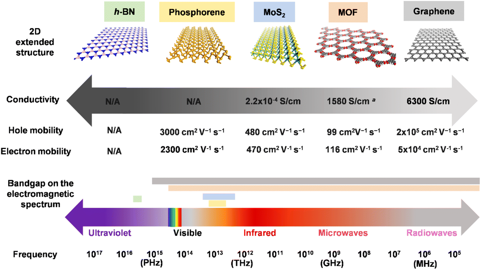 | ||
| Fig. 2 Various atomically thin 2D crystals with corresponding carrier mobilities, conductivities, and electronic bandgap energy.101 2D materials possess a variety of chemical structures, for instance, h-BN,102 MOFs,103 and MoS2,104 contain a mixed structure of elements, while black phosphorus105 and graphene106 are composed of pure elemental sheets. There is a wide range of electronic structures in 2D materials, ranging from insulation in h-BN to metallic conductivity in graphene. The broad spectrum of properties of different 2D materials introduces a paradigm shift in the field of sensing. Adapted with permission from ref. 38 Copyright 2019, the American Chemical Society. | ||
Generally, considering the surface effects of 2D materials, they offer a vast surface area for enhanced molecular interactions, enabling high sensitivity and extremely low detection limits, even for ultralow analyte concentrations. Additionally, the active sites on their surface boost their interaction with the target species and facilitate the immobilization of additional recognition elements, such as metallic nanoparticles (NPs) and receptors. In the case of electrochemical sensing, the presence of active sites endows these materials with electrocatalytic characteristics that enhance the current, while lowering the redox potential in the presence of the analyte. In addition, good selectivity can be achieved using 2D material-based sensors by taking advantage of their rich surface chemistry, which can be enhanced through chemical functionalization or defect engineering.76–78 Furthermore, considering the factors such as sensitivity and selectivity can also enhance the performance of sensors, improving their detection efficiency.79,80 Wang et al. showed that glassy carbon electrodes coated with graphene could increase the faradaic current by 20 times, while lowering the reduction potential of H2O2 by about 0.4 V.77 Another aspect of graphene-based sensors is that there are several approaches to increase their specificity and selectivity. In this case, one practical approach is to decorate the basal plane of graphene with different organic groups and biomolecules, which act as receptors for the analyte of interest.81,82
Here, covalent and non-covalent approaches are the two main categories of surface modification or functionalization techniques (e.g., chemical) commonly used to enhance the sensing potential of 2D materials.79,83,84 Covalent methods are recognized as reliable and allow the attachment of functional groups to the surface of 2D materials, allowing the modification of their crystalline structure and resultant electrical characteristics.85,86 However, although 2D materials exhibit effective selectivity, altering their surface can change their electrical nature, making them poor choices for sensing. Furthermore, the covalent functionalization of graphene has the concomitant drawback of reducing its conductivity. In contrast, flexible non-covalent functionalization enables the modification of the electrical and physical characteristics of 2D materials without affecting their crystalline structure.
Moreover, the non-covalent features of 2D materials can be studied based on their van der Waals, electrostatic, and π–π interactions, which can be used to change the doping concentrations in a controllable way.87 Given that conductivity is a characteristic of graphene and other 2D materials that improves sensitivity, particularly in electrically transduced sensors,38 it is now conceivable to scale miniature devices due to the exceptional charge transport properties of 2D materials, which are preserved in thin sub-nanometer layers. Furthermore, the large lateral dimensions of 2D materials ensure excellent electrical contacts in electronic devices.88
In particular, the exceptional sensing ability of 2D materials in gas sensing can be explained by several of their properties. The entire surface of these materials is available to adsorb gases due to their 2D structure, which maximizes their interaction with the surface. Furthermore, noise reduction is guaranteed by their excellent crystallinity and good conductivity. Also, the low-resistance ohmic connections on graphene allow its simple integration with a range of device topologies. Based on these notions, Novoselov and colleagues demonstrated a sensitive graphene sensor capable of identifying a single gas molecule interacting with its surface.89 The authors showed that graphene is a 2D material that is electrically quiet and suitable for the fabrication of single-electron detectors. 2D materials are excellent candidates for sensing applications due to their above-mentioned physical and chemical characteristics. Presently, a wide variety of top-down and bottom-up synthetic protocols has been created and developed to fine-tune the number of layers, lateral dimensions, composition, and overall quality of 2D materials, enabling their unique qualities to be fine-tuned for a particular application. Due to their accessibility and distinct properties, graphene and TMDCs have been extensively studied for applications in sensing.73,90 However, there are some limitations associated with these materials, particularly in the field of sensing.87
The zero band gap of graphene is a significant disadvantage for any optoelectronic application. Similarly, the application and development of MoS2 is limited by its many shortcomings. Specifically, owing to its high surface energy, the number of electrochemically active sites is reduced by restacking. Also, due to its interaction with oxygen and water, monolayer MoS2 is unstable in the natural environment.91,92 When used for electro(bio)chemical sensing, the sensitivity of MoS2 is limited by its poor electrical conductivity and Young's modulus.93,94 Recently, due to their outstanding characteristics, individual 2D materials, especially graphene and TMDCs, have received increasing attention in the field of chemical sensing. Accordingly, considering the variety of 2D materials available and their various qualities, combining them in hybrid structures can be an effective way to benefit from their common features. In this case, different 2D materials can be stacked to create heterostructures using the same van der Waals interactions that hold the layers of 2D materials together in their bulk crystals. In contrast to individual structures, materials in proximity to the heterojunction exhibit a synergistic effect, resulting in new and improved properties. Furthermore, doping can provide additional control to change the aforementioned physical characteristics of 2D materials. According to Wang et al., doping graphene with heteroatoms can modify its electrocatalytic characteristics, further improving the performance of the fabricated electrodes. Consequently, the electrodes modified with graphene and N-doped graphene showed remarkable sensitivity for the detection of H2O2 and glucose. Additionally, a new class of 2D materials known as MXenes has attracted significant interest from the scientific community and is being extensively investigated for use in sensing applications.95 The tunable surface chemistry and versatile physical properties of MXene introduce new sensing capabilities and successfully circumvent several limitations.
2.1 2D monoelements
The most obvious alternatives to graphene are the other elements in group IVA, which have the same number of electrons. However, 2D materials are an emerging field, and thus their potential has not been fully realized and the degree of their potential properties and highly efficient commercial-level device applications remain untapped.27,96 To date, numerous theoretical calculations have been performed to evaluate their basic properties, while experimental investigations are in their early stage, while practical synthesis methods are being investigated to introduce definite synthetic routes and possible limitations. In this case, the neighboring groups to group IVA (VA and VIA) provide a solution of some of these limitations due to their sizeable bandgap, which is advantageous for logic electronics. One closely associated category of 2D crystals is single-element 2D Xenes, which obtain their etymology from sp2-hybridized alkene bond and usually consist of a single layer of atoms arranged in a honeycomb-like structure.97 The electronic structures of group IVA Xenes, i.e., silicene, germanene, and stanene (where X = Si, Ge, and Sn, respectively), which are regarded as counterparts to graphene, are known to fluctuate remarkably. In particular, group IVA Xenes exhibit isoelectronic properties to graphene. Similarly, up-and-down atomic bulking around their honeycomb structure results in more considerable interatomic distances, providing a novel route toward covalent functionalization.The buckled structure and inherent strong spin-orbital coupling identified in the 2D topological insulators provide a path for an advanced quantum state of matter. In the bulk form, solid-state materials have an insulating electronic configuration and small dissipated conducting channels around all their edges, which are protected from backscattering by time-reversal symmetry. This the 2D topological insulator effect can facilitate the realization of materials with exceptional conductivity and completely shielded from defects and scattering disturbances. The electronic nature and stability of 2D Xenes are significant concerns in realizing realistic Xene-based devices, particularly in sensing. Specifically, free-standing sheets from group IVA elements contain higher consistency under normal conditions, which is a complicated matter. In this case, the use of chemical approaches to control the functional groups present in 2D Xene materials is a viable method for regulating their properties and enhancing their stability. Hence, organic moiety-based functionalization in an ambient temperature and pressure environment is necessary. In nanoelemental nanosheets, every atom in their structure is covalently bonded with a ligand, which cancels out the π bonding. In this case, the ligand pairs covalently with the half-filled Pz-orbital to create a gap.
Also, the semiconducting bandgap configuration and its size are determined by the ligand and the skeleton elements. A buckled structure can be chemically altered by replacing its hydrogen atoms with organic functional groups. Organo-modified graphene quantum dots, germanane, silicane, and other theoretically estimated free-standing 2D group-IV “Xene” materials are very similar. Thus, chemically modified, self-supporting 2D Xene materials are excellent candidates for a nanotechnological strategy that incorporates metaphysical aspects for basic research and application. The fabrication of various silicene and germanene Bi-layer frameworks has been demonstrated both theoretically and experimentally. Some practical conditions, such as external charge distribution and surface stress, determine the formation of these structures. Surface-substituted ligands usually achieve structural flexibility in the entire region between different nanoscale materials. Primarily, carbon atoms form a strong covalent bond between them owing to their various hybridization states (sp, sp2, and sp3), which enable the development of structures with varying arrangements. The various carbon allotropes are well-developed, and among them, the planar honeycomb lattice is the most attractive. Although 2D graphene has a perfect carbon atom arrangement, its gapless structure limits its practical use in nanodevices. Alternatively, due to their high quantum confinement and edge effects, functionalized graphene and nano-sized graphene fragments can be used in bandgap applications. Quantum confinement exists in graphene regardless of its size, which results in intriguing behaviors that do not appear in typical semiconducting nanocrystals. Usually, an oxygen-rich environment results in the oxidation of 2D Xenes,98,99 while ultrahigh vacuum can drastically reduce this phenomenon.99 However, the decomposition mechanism is unclear, and oxidation may still occur through other atmospheric molecules, such as water.100
| Materials | Properties | Applications | ||||
|---|---|---|---|---|---|---|
| Conductivity charge mobility | Band structure and bandgap | Chemical stability | Surface functionalization | Biocompatibility cytotoxicity | ||
| Abbreviations: BL = bilayer, SL = single layer.a According to ab initio calculations, the bandgap is predicted to be metallic, while other properties are yet to be determined. However, the initial study only reports its superconductivity.b MBenes have prominent Fermi states and are metallic; however, thorough studies are required to determine a figure of merit.c According to the preliminary reports on MBenes, it is easy to terminate the MBenes surface with O, OH, and F functional groups after exfoliating from their bulk MAB phases. However, few theoretical studies suggest that functionalized MBenes have better redox electrochemistry and have potential in lithium–sulfur batteries.136d So far, the cytotoxicity and biocompatibility of 2D MBenes have not been extensively investigated and should be explored further.e Molecular dynamic simulations were performed on the prevention of Aβ amyloid aggregation (a potential biomarker of Alzheimer's and Parkinson's disease).f Ti3C2Tx produced by EN-MILD method.g In sp2 hybridized graphene, π-electrons move freely on the surface, providing a high electron transfer rate that makes it suitable to fabricate electrochemical transducers.137 | ||||||
| TMCCs | Recently discovered family of 2D materialsa | To be determined | ||||
| MBenes | Metallic conductivity43 | Metallic107,b | Manifest outstanding stability in aqueous media at ambient conditions107 | No experimental evidence shows the presence of terminal groups on the surface of MBenesc | Better compatibility and negligible cytotoxicityd | In silico study on amyloid-β deformation45,e |
| MXenes | Up to 2.4 × 10⁴ S cm−1 | Tunable bandgap via intercalation and terminations109,110 | Offer a homogeneous suspension in aqueous solutions; however, susceptible to oxidation under ambient conditions and/or in an oxygen-rich environment95,112 | Abundant intrinsic surface terminations offer profuse loading of analyte-sensitive species for biorecognition and VOC sensing95,113–115 | Biocompatible and negligible cytotoxicity116,117 | Electrochemical, optical, gas, stress/strain sensors, and many biomedical applications118,119 |
| DC conductivity of ≈9880 S cm−1 in Ti3C2Tx films produced by spin coating108,f | Bare MXenes are metallic, while terminated ones are predicted to be semiconducting111 | |||||
| Metallic for Ti3C2 | ||||||
| Graphene | Carrier mobility in the order of 103 at RT120 | Unique structure with zero band gap (BL graphene) but tunable up to 250meV121,122,g |
GO has improved dispersion in aqueous solutions and is relatively stable123 | However, no intrinsic surface termination in pristine graphene can be functionalized for sensing applications124,125 | Cytotoxic have biosafety concerns126,127 | Do76,128 |
| TMDCs | (i) SL MoS2 has charge mobility of 200 cm2 V−1 s−1 at RT129 | Tunable bandgaps130 | Degradation occurs in a moisture and oxygen environment131 | Lacking intrinsic surface functionalization of external species linkage132 | TMDCs have variable cytotoxicity reported133,134 | Do19,135 |
| (ii) The conductivity of 5.0 S cm−1 (MoS2)130 | SL MoS2 = 1.8 eV | |||||
| SL WS2 = 1.45 eV | ||||||
| SL WSe2 = 1.7 eV | ||||||
3 Various sensing platforms
Sensing is essential to monitor harmful environmental chemicals, detect toxic gases, diagnose diseases, and monitor human health. Thus, the development of robust and efficient sensing systems to detect specific analytes (chemical and/or biological) such as gases, toxic ions, chemicals, and biomolecules, while maintaining stability, sensitivity, and selectivity for particular domains is critical in various applications. In this section, we introduce various 2D materials to create sensor systems, including electrical, fluorescence, electrochemical, and biomedical sensors. 2D materials, including graphene and TMDCs enable the development of different sensing platforms to detect a variety of external species owing to their excellent conductivity, wide effective surface area, enhanced sensitivity, and exceptional potential to quench the fluorescence signal.3.1 Gas sensors
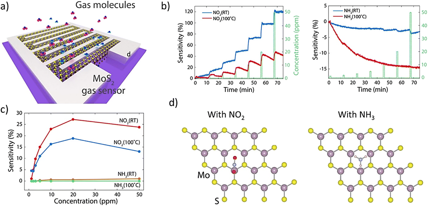 | ||
| Fig. 3 (a) 3D schematic of the interdigitated electrode of MoS2 on sapphire. (b) Transient cure for NO2 (left) and NH3 (right) gas response from 1.5 to 50 ppm gas, operating at room temperature and 100 °C. In the NO2 gas mode, the resistance increased (positive sensitivity). (c) Sensitivity comparison of NO2 and NH3 gases at different gas concentrations and operating temperatures and (d) top views of the most favorable configurations for NO2 (left) and NH3 (right) on MoS2. Adapted with permission from ref. 144 Copyright 2015, Nature Publishing Group. | ||
 | ||
| Fig. 4 Schematic of the fabrication of SAW devices: (a) GO layer-coated clean surface, (b) GO layer in the center, and (c) completely covered with GO. SEM micrographs of interdigitated transducers (IDTs): (d) GO layer coated clean surface, (e) GO layer in the center, and (f) completely covered with GO. Adapted with permission from ref. 151 Copyright 2014, Nature Publishing Group. | ||
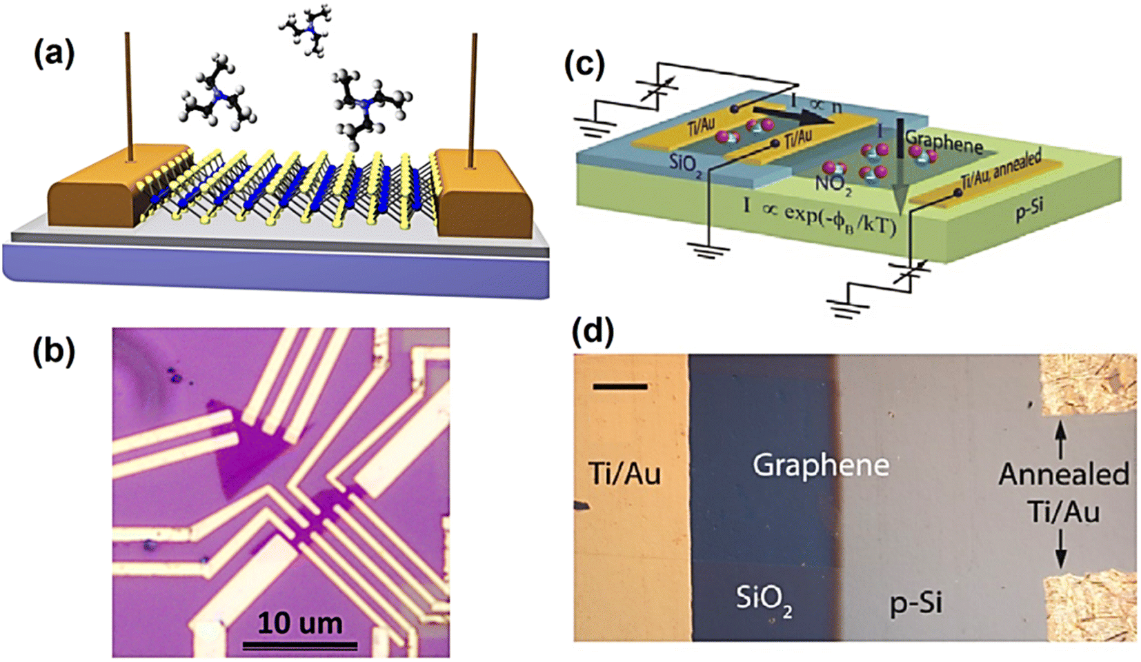 | ||
| Fig. 5 (a) Schematic of a conductometric sensor and (b) optical image of MoS2 monolayer-based conductometric sensor translated on SiO2/Si substrate. Adapted with permission from ref. 29 Copyright 2013, the American Chemical Society. (c) Schematic of the graphene/Si Schottky device fabricated on the same chip. (d) Optical image of graphene/p-Si Schottky diode. This illustrates that graphene is transported over SiO2 substrate with Ti/Au contacts and p-Si with annealed Ti/Au contact. (Note: scale bar = 200 μm). Adapted with permission from ref. 158 Copyright 2014, John Wiley & Son. | ||
| Materials | Synthesis route | Sensing platform | Gases | LOD | Sensitivity | Response time | Ref. |
|---|---|---|---|---|---|---|---|
| Abbreviations: ppm = parts per million, NRs = nanorings, PEI = polyethylenimine, DMSO = dimethyl sulfoxide, TFT = thin film transistor, HCHO = formaldehyde, and TMA = trimethylamine. | |||||||
| MoS2 | CVD | MoS2 FET | NO2 | 20 ppb (NO2) | >40% | 5–9 min | 160 |
| NH3 | 1 ppm (NH3) | ||||||
| CVD | MoS2 | CO | 500 ppm (CO) | — | — | 161 | |
| CO2 | 5000 (CO2) | ||||||
| CVD | MoS2 | NO2 | 0.1 ppb | 3.3/ppb (3300/ppm) | — | 162 | |
| Solvothermal & in situ polymerization | PANI/MoS2/SnO2 | NH3 | 200 ppb | — | 10.9 s (100 ppm) | 163 | |
| Hydrothermal | Co-MoS2 | NO2 | 100 ppm | — | 10 s (100 ppm) | 164 | |
| Intercalation-assisted exfoliation | MoS2 TFT | NO2 | 2 ppb | — | >30 min | 165 | |
| Micromechanical exfoliation | MoS2 | NO2 | — | NO2 – 1372% | 30 min | 166 | |
| NH3 | NH3 – 86% (1000 ppm) | ||||||
| Mechanical exfoliation | MoS2/GaSe | NO2 | 20 ppb | 6.3% (20 ppb) | 23 s | 167 | |
| — | |||||||
| Hydrothermal | MoS2@SnO2 nanocomposite | NO2 | 10 ppm | — | 2.2 s | 168 | |
| Drop-casting | MoS2/ZnO nanohybrid | NO2 | 0.2 ppb | 0.135 ppb | 132 s | 169 | |
| WS2 | Drop coated and | Au-SnO2-co-decorated WS2 NS | CO | — | — | 3.687 (50 ppm) | 170 |
| Wet-chemical precipitation | WS2/PbS | NO2 | ∼20 ppb | — | 8.8% | 171 | |
| Hydrothermal | WS2/MWCNTs | TMA | 76 ppb | — | — | 172 | |
| Liquid exfoliation | WS2 nanosheets | NO2 | 10 ppm | — | 45 s (10 ppm) | 173 | |
| 8 ppm | 11 s (8 ppm) | ||||||
| Hydrothermal | WS2/CuO | NH3 | 5 ppm | — | 40.5% (5 ppm) | 174 | |
| g-C3N4 | Electron beam evaporation. | g-C3N4/GaN NRs | NO2 | — | — | 42.24% (5 ppm) | 175 |
| Poly condensation | g-C3N4 – C/g-C3N4 | NO2 | 50 ppm | — | 71.36% (50 ppm) | 176 | |
| MXene | In situ growth | TiO2/Ti3C2Tx | NH3 | 30 ppm | — | 5 ppb | 177 |
| Ultrasonic spray pyrolysis | Ti3C2Tx/ZnO | NO2 | 100 ppm NO2 | — | — | 178 | |
| Wet chemical precipitation | MXene/Co3O4 | HCHO | 0.01 ppm | — | 9.2 (10 ppm) | 179 | |
| Hydrothermal | SnO2/MXene | NO2 | 30 ppb | — | 146 s | 180 | |
| Hydrothermal | SnO–SnO2/Ti3C2Tx | Acetone | 100 ppm | — | 12.1 s | 181 | |
| LiF + HCl | Ti3C2Tx/WO3 | NO2 | 50 ppm | — | 510% (50 ppm) | 182 | |
| Hydrothermal | Co3O4@PEI/Ti3C2Tx | NOx | 30 ppb | — | >2 s | 183 | |
| DMSO-treated Ti3C2 etched powder | Ti3C2Tx MXene | NH3 | 500 ppm | — | 67 s | 184 | |
3.2 Electrochemical sensors
The evolution of sensor devices has witnessed tremendous growth, leading to the development of numerous sensors exhibiting different sensing mechanisms. Among them, electrochemical sensors, which are sensors in which an electrode acts as a transducer element in the presence of an analyte, are popular preferences because of their documented inherent accuracies. Further, considering their high device sensitivity, instantaneous response, and easy-to-use set-up, these sensor devices are an attractive choice as analytic platforms.185 The functioning mechanism of these types of sensors relies on detecting the electrochemical reactions between the electrode surface and analytes. Generally, they convert chemical concentrations into quantitative electric signals, the magnitude of which equals the chemical concentration levels. Typically, the measurements using these sensors are based on amperometry, potentiometry, and conductometric. However, not all analytes can induce redox reactions, and thus external mediators are necessary to generate electrochemical signals proportional to the analyte concentration.186 Consequently, a specific working electrode design modified with 2D materials can improve the quantitative measurement of electrochemical signals during a particular analyte-antigen interaction.187,188In electrochemical sensing devices, the primary detection mechanism involves the transfer of electrons from the active material deposited/coated on the working electrode in a tri-electrode functional structure immersed in an electrolytic-containing solution. In the case of gas sensors, the gases diffuse through a membrane, leading to their oxidation and/or reduction on the electrode surface. In electrochemical sensors, three distinct types of signals can be obtained using three distinct methodologies, including cyclic voltammetry (CV), amperometry, and differential pulse voltammetry. A large effective surface area, exceptional electrical conductivity, and intrinsic redox potential are imperative parameters that determine the efficiency of electrode materials. Extensive investigations have been conducted on the use of nanomaterials as active sensing materials because of their significant advantages compared to their bulk counterparts. Their small size and large surface area make them ideal for mass transfer and their enhanced signal-to-noise ratio are the major characteristics of electrochemical sensors exploited thus far.189,190 Also, 2D materials are widely employed as sensing electrodes in electrochemical sensors because of their inherent electrical conductivity, outstanding electrochemical characteristics, and substantial surface-to-volume ratios.191,192 Recently, 2D graphene and its derivatives, such as rGO (reduced graphene oxide) have emerged as commonly used forms of graphene in electrochemical sensors. Realizing the impact of using graphene in electrochemical sensors,193 in this part, we focus on introducing other 2D materials besides derivates of graphene for electrochemical sensing. A wide variety of 2D materials besides graphene has been reported thus far. Among them, MoS2, WS2, SnS2, FeS2, and Ni3S2 have been recently utilized as sensing electrodes to determine various analytes.194 Zhang et al. reported the use of a monolayer MoS2 nanosheet as an electrochemical electrode for glucose detection. MoS2 exhibited good redox activity and electrochemically reduced MoS2 (r-MoS2), providing efficient electron transport and better conductivity in different electrolytes, e.g., [[Ru(NH3)6]2+/3+ and Fe[(CN)6]3−/4−] redox system. The proposed sensor was employed to detect dopamine (DA) and showed good selectivity for DA in a mixture of uric acid and ascorbic acid as interfering agents.195 Here, it is important to emphasize that pristine TMDC nanosheets do not often exhibit superior sensing properties due to their poor electrical conductivity. Thus, one of the approaches to increase their sensitivity is synthesizing hybrid nanosheets with rare-earth metal NPs (Au, Ag, Pt, and Pd). The synergistic effects between the surface of TMDCs and NPs can improve their electrocatalytic behavior and sensitivity compared with pure TMDC nanosheets.194,196 Similarly, this can be applied to various 2D materials that lack the required electrical conductivity for sensitive and selective electrochemical sensing. The quest to develop state-of-the-art electrochemical sensing materials has also witnessed the application of MXenes as electrode materials for chemical signal transduction. Metal-like electrical conductivity, intrinsic surface terminations, redox-active sites, ample surface termination that allows copious mass loading, and large surface area enable the rapid transduction of chemical signals. Zhu et al. fabricated a hemoglobin (Hb)-immobilized mediator-free Ti3C2-MXene-based electrochemical sensor,197 which showed excellent capability towards nitrite detection with an LOD as low as 0.12 μM and a wide linear range (0.5–1800 μM). Besides 2D inorganic materials, Zhang et al. described the application of 2D MOF nanosheet-based electrodes for H2O2 detection.198 Using the Langmuir–Schafer method, 2D M-TCPP (Fe) nanosheets (M = Co, Cu, and Zn) were produced in the form of thin films on electrodes (Fig. 6a). It is important to mention that the electrode composed of Co-TCPP(Fe) nanosheet showed the best electrocatalytic activities among the structures, together with a low LOD of 0.15 × 10⁶ M (Fig. 6b). Furthermore, the proposed electrochemical sensor could be used to real-time monitor H2O2 production by live cells (Fig. 6c). A 2D bimetallic organo-metal-framework was successfully synthesized with a bio-inspired design of organic ligands and metallic nodes and used as sophisticated 2D biomimetic nanomaterials (Fig. 6d).198 More electrochemical sensors based on novel 2D materials are expected to be fabricated in the future. In addition, Table 4 presents the application of various 2D materials as efficient sensing platforms. However, despite the remarkable success of 2D material-based electrochemical sensors, they have certain limitations. Firstly, given that several 2D materials have been employed thus far, their poor electrical conductivity often results in a low detection limit. The growth of rare earth metal NPs on the surfaces of 2D materials can enhance electrical conductivity and redox activity, resulting in improved sensing performances. Contrarily, the application of noble metal NPs is not cost-efficient and can increase the fabrication costs. In this case, modification of the crystalline phases is an alternative approach to address the poor electrical conductivity associated with 2D TMDC materials. For example, 1T phase TMDC metal nanosheets have higher electrical conductivity than 2H phase nanosheets, and thus a phase transformation can comprehensively overcome this limitation. A further shortcoming of electrochemical sensors that utilize 2D materials as electrode materials is their limited long-term stability, which needs to be carefully addressed.
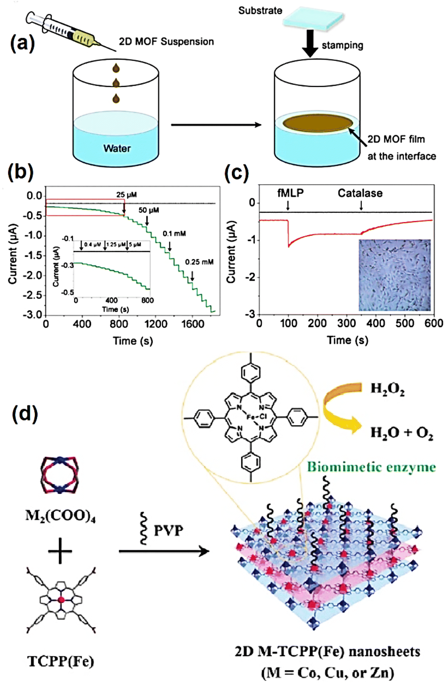 | ||
| Fig. 6 (a) Illustration of 2D MOF nanosheet electrode growth via the assembly route, (b) amperometric (I–T) response of the electrodes composed of 2D Co-TCPP (Fe) nanosheet and pristine GCE with different H2O2 concentrations, and (c) I–T response of electrodes composed of 2D Co-TCPP (Fe) nanosheet with 300 U mL−1 catalase and 10 μM fMLP with (asymmetrical red curve) and without (linear black curve) MDA-MB-231 cells. (Inset corresponds to the micrograph of MDA cells using bright-field microscopy.) (d) Schematic of the bio-inspired design of metallic nodes and organic ligands. Adapted with permission from ref. 198 Copyright 2016, John Wiley & Sons. | ||
| Material | Synthesis route | Sensing platform | Analyte | LOD | Linear range | Sensitivity | Ref. |
|---|---|---|---|---|---|---|---|
| Abbreviations: TPT = topotecan, TCAA = trichloroacetic acid, DA = dopamine, PSA = prostate-specific antigen, BPA = bisphenol A, As(III) = arsenic(III), MIP = molecularly imprinted polymers, and SPCE = screen-printed carbon electrode. | |||||||
| MoS2 | Hydrothermal | AuNPs/MoS2/graphene | NO2− | 1.0 μM | 5.0 μM to 5.0 mM | — | 199 |
| Hydrothermal | MoS2/TiO2 | TPT | 9.8 nM | 0.01–18.57 μM | — | 200 | |
| Hydrothermal | AuNPs-MoS2/graphene | Rutin | 0.01–45.0 μmol L−1 | 0.004 μmol L−1 | — | 201 | |
| Chemical exfoliation | MIP/MoS2/NH2-MWCNT@COF/GCE | Sulfamerazine | 1.1×10⁻⁷ mol L−1 |
— | — | 202 | |
| Chemical exfoliation | Ag nanoprism@MoS2 | TCCA | 0.17μM |
0.5–10μM & 10−80μM |
— | 203 | |
| — | MoS2-AuPt | Pb2+ ions | 38 fg mL−1 | 0.1 pg mL−1 to 1000 ng mL−1 | 204 | ||
| WS2 | Chemical exfoliation | WS2/CNTs | Isoniazid | 0.24 μM | 10–80 μM | — | 205 |
| Li intercalation | WS2-MIPs/GO-SWCNTs/GCE | Vitamin B2 | 0.0007 μM | 0.002–0.9 μM | 12.539 μA μM−1 | 206 | |
| Hydrothermal and seed-mediated growth | Pt-Ag/WS2 | DA | 0.2 μM | 0.6 μM to 1 mM | 348.8 μA mM−1 cm−2 | 207 | |
| Hydrothermal | WS2/GdCoO3 | Quercetin | 0.003 μM | 0.001–329 μM | 6.922 μA μM−1 cm−2 | 208 | |
| Sonochemical | MP-WS2 NRs/SPCE | Clonazepam | 2.37 nM | 10–551 μM | 24.32 μA μM−1 cm−2 | 209 | |
| g-C3N4 | Pyrolysis technique | g-C3N4/CuO | DA | 1.00 × 10⁻¹⁰ mol L−1 | 2.00 × 10⁻⁹ to 7.11 × 10⁻⁵ mol L−1 | 0.316 μA cm−2 μmol L−1 | 210 |
| Calcination | ZIF-8/g-C3N4/Co | D&C red 33 | 0.034 μM | 0.08–10 μM to 10–900 μM | — | 211 | |
| Patent Blue V | |||||||
| Sol-Gel | g-C3N4 | H2O2 | 26.48 μM | 150 nM to 1.8 μM | 27 μA cm−2 μM−1 | 212 | |
| — | C3N4 NTs/ionic liquid | Ractopamine | 1.0 × 10⁻¹³ M | 1.0 × 10⁻⁹ to 1.0 × 10⁻¹² M | — | 213 | |
| Pyrolyzing thiourea | HP5@AuNPs@g-C3N4 | PSA | 0.12 pg mL−1 | 0.0005–10.00 ng mL−1 | — | 214 | |
| Solvothermal | g-C3N4 and Ru@MOFs | Amyloid-β | 3.9 fg mL−1 | 10−5 to 500 ng mL−1 | — | 215 | |
| Sonochemical | g-C3N4/NiO | Quercetin | 0.002 μM | 0.010–250 μM | — | 216 | |
| MOF | Hydrothermal | Au@Cu-MOF/N-GQDs/GCE | Patulin | 0.0007 ng mL−1 | 0.001–70.0 ng mL−1 | — | 217 |
| Hydrothermal | Cu-MOF/rGO/CuO/α-MnO2 | Resorcinol | 0.2 μM | 0.2–22 μM | 6262.6 mM cm2 | 218 | |
| Hydrothermal | NiO@Ni-MOF | Luteolin | 3 pM | 0.01–1 nM & 1 nM to 50 μM | — | 219 | |
| In situ preparation | Ni-MOF@CNTs hybrid | BPA | 0.35 nM | 1–1000 nM | 284.64 μA μM−1 cm−2 | 220 | |
| Chemical exfoliation | Hemin@MOF | H2O2 | 0.07 μmol·L−1 | 0.1–2200 μmol·L−1 | — | 221 | |
| Hydrothermal | GO/MOF | As(III) | 0.06 ppb | 0.2–25 ppb | — | 222 | |
| Hydrothermal | SnS@Co N-C microrod | L-Tyrosine | 3.1 nmol L−1 | 0.01–250.0 μmol L−1 | — | 223 | |
| Electrospun | Mn MoO4-MXene | Hydroquinone | 0.26 nM | 5–65 nM f | 7.437μA nM−1 cm−2, 6.471 μA nM−1 cm−2 |
224 | |
| MXenes | Catechol | 0.30 nM | |||||
| Hydrothermal | Fe-MOF/MXene | As(III) | 0.58 ngL−1 | 10 ∼ 100 ngL−1 | 8.94 μA/ng L−1 cm−2 | 225 | |
| HF etching and others | Ti3C2/G-MWCNTs/ZnO | DA | 3.3 nM | 0.01–30 μM | 16 A/M | 226 | |
| HF etching | AuNPs@Ti3C2 | 5-Hydroxymethylcytosine | 0.632 pM | 0.632 to 63.2 pM | — | 227 | |
| LiF + HCL | Ti3C2@N-C | Cd2+ | 2.55 nM | 0.1–4 μM | 49.8500 μA nM−1 cm−2 | 228 | |
| Pb2+ | 1.10 nM | 0.05–2 μM | 177.3327 μA nM−1 cm−2 | ||||
| — | MIP/Cu-MOF/Ti3C2Tx/GCE | Hygromycin-B | 1.92 nM | 5 nM to 5 μM | — | 229 | |
| Electropolymerization | MIP/CNT/Cu2O NPs/Ti3C2Tx | Diethylstilbestrol | 6 nM | 0.01–70 μM | — | 230 | |
| Wet precipitation | Ti3C2Tx-Cu2O | Glucose | 2.83 μM | 0.01–30 mM | 11.061 μA nM−1 cm−2 | 231 | |
| — | Ce-MOF/Ti3C2Tx | L-Tryptophan | 0.19 μM | 0.2–139 μM | 0.1556 μA nM−1 cm−2 | 232 | |
3.3 Wearable sensors
In recent years, wearable electrochemical sensors have gained a lot of interest due to their ability to real-time human health monitoring. Several biomarkers in sweat can provide information to monitor the physiological health of an individual. Meng et al. reported the fabrication of an electrochemical sensor for real-time sweat analysis using a highly integrated sensing paper.233 The device was fabricated by following a simple printing procedure, including highly integrating sensing paper with a hydrophobic protective wax and a conductive electrode array and incorporating MXene/methylene blue (Ti3C2Tx/MB) as the active material. For the fabrication of the sensor, an aqueous dispersion of Ti3C2Tx-MXene was drop-casted on screen-printed carbon electrodes followed by the immobilization of chitosan-contained glucose oxidase (GOx) solution. The proposed sensor showed good sensitivity and selectivity towards the simultaneous determination of lactate and glucose with an LOD of 0.49 μA mM−1 and 4 nA μM−1, respectively. Ti3C2Tx exhibited excellent adsorption capability due to its large surface area and methylene blue modification synergistically increased the electrochemical response of the device.234–236 The proposed highly integrated sensing paper-based sensor has enormous potential in wearable bioelectronic products and can be employed to develop innovative smart technologies. Recently, Lu et al. reported the fabrication of a flexible pressure sensor (MoS2/CSilk) using vertically aligned MoS2 nanosheets on carbonized silk (CSilk) fabric.237 After a pyrolytic reaction, carbonized fibers with highly conductive sp2 hybrid graphite structures were produced from the commercially available silk fiber. The MoS2/CSilk hierarchical structure was obtained after a two-step solvothermal reaction. In the first step, for the in situ production of MoS2 on the fibers, urea, MoO3, and thioacetamide were added as precursors with a concentration of 0.3 g, 60 mg, and 70 mg, respectively, in a mixture of ethanol (25 mL) and deionized water (15 mL) and stirred vigorously for one hour. In the second step, the ultra-sonicated carbonized silk fiber was soaked in the above-mentioned mixture and the whole solution was hydrothermally treated for 24 h at 220 °C. The prepared MoS2/CSilk fiber was repeatedly rinsed with water, and then ethanol and left overnight to dry at 60 °C.237 The pressure sensor was made up of two MoS2/CSilk thin films arranged face to face and packed using 3 M VHB 9469 (double-sided adhesive tape model).237 The contact area between the two MoS2/CSilk thin films varied upon the application of pressure, resulting in variations in the contact resistance. Thus, the loading pressure could be determined by monitoring the variations in electrical signals (Fig. 7). This sensor can be combined with wearable systems or self-powered appliances. Owing to its exceptional performance, the pressure sensor composed of MoS2/CSilk can be utilized for real-time physiology monitoring and possibly clinical diagnostics.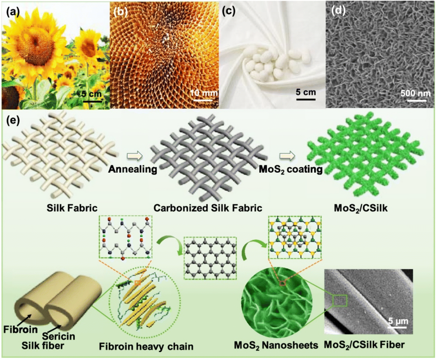 | ||
| Fig. 7 Architecture, fabrication process, and structural variations of MoS2/C Silk. (a and b) Digital photographs of a sunflower faceplate, (c) commercially available silk fabric, (d) SEM images of MoS2/CSilk and (e) demonstration of synthesis strategy and structural alterations. Adapted with permission from ref. 237 Copyright 2020, the American Chemical Society. | ||
Further, Shin et al. proposed a sensor based on MoS2 sandwiched between two Au-layers (Au/MoS2/Au) on polyethylene terephthalate (PET) for the detection of HIV-1 surface proteins, e.g., glycoprotein GP120.238 The surface of HIV consists of non-covalently bonded envelope glycoproteins GP120 (gp120) and GP41 (gp41). Thus, the early detection of Gp120 is crucial given that it binds to the cluster and plays a significant role in HIV infection. To realize this type of biosensor, PET substrate was coated with Au monolayers through sputtering (Au/PET), and then MoS2 NPs were spin-coated on the Au-coated PET substrate (MoS2/Au/PET). In the final step, the substrate was again coated with Au via sputtering (Au/MoS2/Au/PET).238 GP120 antibody was immobilized on the electrode via the cysteamine-modified Au/MoS2/Au surface. Spectroscopic analysis and SEM, AFM, and CV measurements were performed to confirm the fabrication of the sensor. Analyte detection was performed through square wave voltammetry, and the proposed flexible sensor showed great sensitivity and selectivity with an LOD of 0.1 pg mL−1.238 Wang et al. reported the fabrication of an electrochemical sweat platform based on freestanding graphene paper (GP) decorated with MoS2 nanocrystal monolayers and submicron Cu-buds for the bifunctional detection of lactate and glucose.239 The sensing electrode was fabricated via the sequential growth of 0D-MoS2-nanocrystals on 2D freestanding GP employing the hydrothermal process, followed by the electrodeposition of 3D Cu submicron-buds. The GP ensured effective charge transfer towards the working electrode, while the triple component (Cu-MoS2-GP) structure was coated with lactate oxidase, which offered a favorable microenvironment for enzyme immobilization, and also facilitated the charge transfer. The fabricated electrodes (lactate oxidase-Cu-MoS2-GP) exhibited bifunctional sensing with high electrocatalytic activity, long stability, and reproducibility. The proposed electrochemical sensor showed a broad linear range, with values varying in the range of 0.01–18.4 mM for lactate and 5–1775 μM for glucose, with detection limits of 0.1 μM and 500 nM. In contrast, the sensitivity for lactate and glucose was reported to be 83 mA cm−2 μM−1 and 3.38 mA cm−2 μM−1, respectively. Certainly, this sensor device fabricated by integrating 0D-transition metal sulfide, 2D-graphene, and 3D-transition metal can provide a new pathway to fabricate sensors to monitor glucose and lactate in sweat.239 Wang et al. also proposed a non-enzymatic flexible MOF electrode-based sensor by effectively integrating self-assembled and oriented Cu3(btc)2 nanocubes with amino-functionalized free-standing GP (Cu3(btc)2-NH2-GP).240
Compared to similar enzyme-based sensors for lactate and glucose monitoring in sweat, the proposed sensors provided a wide dynamic range (0.05 mM to 22.6 mM for lactate and 0.05–1775.5 μM for glucose) with a considerably low lactate oxidase (5 μM for lactate and 30 nM for glucose). However, it is essential to note that the proposed sensors exhibited greater sensitivity with a value of 0.029 mA cm−2 μM−1 for lactate and 5.36 mA cm−2 μM−1 for glucose, respectively.239 This increase in sensitivity can be attributed to the proximity effect between the closely packed Cu3(btc)2 nanocubes and functionalized graphene nanosheets, resulting in conductive pathways. In addition, coupled with the ideal microenvironment created by graphene sheets, the small-size Cu3(btc)2 nanocubes enabled the effective transmission of ions towards the transducer by reducing the ion-diffusion length, thus increasing the overall electron transfer kinetics. For the electrochemical detection of glucose, another similar technique has been utilized in the case of a GOx-immobilized polymer electrode (Kapton® polyimide film) with gold, MoS2, and gold nanofilm (Au/MoS2/Au-nanofilm).241 This sensor was fabricated by coating the pre-treated polymer substrate with Au via the Au-sputtering technique, followed by the spin coating of MoS2 NPs (MoS2/Au-nanofilm). Subsequently, a layer of Au was coated again to fabricate Au/MoS2/Au-nanofilm polymer electrodes. A chemical linker (6-MHA) was deposited utilizing Au–thiol binding feature to immobilize GOx on the electrode surface (GOx/Au/MoS2/Au-nanofilm) (Fig. 8). Amperometric (I–T) measurements were performed for the quantitative determination of glucose, which showed an LOD of 10 nM with a linear range of 500 nM to 10 nM. The proposed sensors showed good selectivity towards glucose sensing in a mixture of uric acid and ascorbic acid as interfering agents. The synergistic effects imparted by Au and MoS2 NPs caused enhanced electrocatalytic activity and increased flexibility could be derived from the polymer.
 | ||
| Fig. 8 Illustration of protocol for the fabrication of an electrochemical biosensor for glucose determination. Adapted with permission from ref. 241 Copyright 2019, Elsevier B.V. | ||
3.4 Electronic and optical sensors
| Materials | Synthesis route | Sensing platform | Analyte | LOD | RH range | Sensing response/sensitivity | Ref. |
|---|---|---|---|---|---|---|---|
| Abbreviations: NS = nanosheets, NH = nanohybrid, ML = multilayers, FL = few layers, QDs = quantum dots, SVE = sulfur-vacancy-enriched, QCM = quartz crystal microbalance, NMP = N-methyl-pyrrolidone, PEI = polyethyleneimine, PMMA = polymethyl-methacrylate, PEO = polyethylene oxide, PE = polyelectrolyte, and LbL = layer-by-layer. | |||||||
| MoS2 | Ultrasonicated exfoliation | MoS2 NS | Soil moisture | — | 11–96% | 43684% |
247 |
| Probe assisted sonication | MoS2 NS | NO2 | 27 ppb | — | 88% (∼8 times) | 248 | |
| Ultrasonicated exfoliation | MoS2 QDs@NMP | Humidity | — | 10–95% | 2.21 MΩ/% RH | 249 | |
| Ultrasonicated exfoliation | MoS2 QDs | Humidity | — | 10–95% | 2.78 MΩ/% RH | ||
| Hydrothermal | SnO2@MoS2 NS | NH3 | — | — | 2083%/200 ppm | 250 | |
| Hydrothermal | SVE MoS2 | NO2 | 0.1 ppb | — | 226% to 200 ppb | 251 | |
| Commercial MoS2 dispersion | MoS2/Nafion/QCM | Humidity | — | 11.3–97.3% | 138.1 Hz/% RH | 252 | |
| Hydrothermal | Cu2O/MoS2 NS | NH3 | — | — | ∼872%/100 ppm | 253 | |
| Liquid phase exfoliation | MoS2 | Formic acid | 50 ppm | — | 0.114pm/ppm |
254 | |
| Mechanical exfoliation | FL MoS2 | NO2 | 5 ppm | — | 4.4 s/5 ppm | 255 | |
| Ultra-sonication | MoS2 | NH3 | — | — | 15.2% | 256 | |
| PMMA-MoS2 | NH3 | 500 ppm | — | 54% | 256 | ||
| Liquid phase exfoliation | MoS2-PEO | Humidity | 10% RH | 10% RH | ∼25% at 10% RH | 257 | |
| 70% RH | |||||||
| Liquid phase exfoliation | MoS2/ZnO | NO2 | 5 ppm | — | 3050%/5 ppm | 258 | |
| WS2 | Probe sonication | ZnO NRs/WS2 NS | Humidity | — | 18–85% | 101.71 fF/% RH | 259 |
| Wet chemical | WS2 NS | Humidity | — | 25–75% | 44.3%/RH% | 260 | |
| Wet chemical | Au@WS2 NS | Humidity | — | 55–75% | 3007.9%/RH% | 260 | |
| Exfoliation | WS2 NS | Humidity | — | 30–70% | 50%/RH% | 261 | |
| Sulfurization | WS2 NS | NO2 | 0.5 ppm | — | NO2 41%/0.5 ppm | 262 | |
| Precipitation | Au-SNO2@WS2 NS | CO | 50 ppm | — | 3.687%/50 ppm | 170 | |
| Hydrothermal | WS2-modified SNO2 hybrid | Humidity | — | 11–95% | 263 | ||
| MXene | LiF + HCl | MXene NS/QCM | Humidity | 1.2% RH | 1–16% RH | 12.8 Hz/% RH | 264 |
| LbL assembly | MXene/PEI-ML | Humidity | — | 10–70% RH | — | 265 | |
| Etching/Mixing | rGO/N-Ti3C2Tx/PEI | CO2 | 8 ppm | <62% | — | 266 | |
 | ||
| Fig. 9 (a) Illustration of experimental arrangement to fabricate WS2 CSPF sensor for humidity sensing, (b) length of the polished area (15 mm) with RFT of ∼70 μm in the polished region, (c) trend of relative power as a function of time through WS2CSPF, and (d) comparison between relative power of WS2CSPF and SPF in comparison with RH. Adapted with permission from ref. 244 Copyright 2016, Optica Publishing Group. | ||
Furthermore, Fig. 9c and d demonstrate a comparison of the humidity response between the bare SPF and WS2SPF humidity sensors. It is evident that the sensitivity of WS2SPF (0.1213 dB/% RH for descending and 0.1056 dB/% RH for ascending) was 15-fold greater than that of the bare SPF (0.0051 dB/% RH for descending and 0.0070 dB/% RH for ascending). The fundamental method for humidity detection based on the WS2CSPF optical sensor is as follows: whenever the chamber humidity increases, the concentration of H2O molecules in the air also rises. Air molecules get physically adsorbed on the WS2 surface, which leads to a small amount of charge transfer from WS2 to H2O. Following the orbital mixing theory,245 the conductivity drops because of the reduction in conducting electrons following a rise in humidity, resulting in a decrease in light absorption. In this case, the transmitted optical output power of an SPF coated with WS2 film increases, followed by a decrease in the transmitted loss of the SPF.
The 2D WS2 coating significantly increased the sensitivity and stability of the optical SPF humidity sensing device. Consequently, the application of WS2 increased the stability and sensitivity of the proposed humidity sensor with a significant figure of merit. The proposed sensors showed (i) an optical power output variation of ∼6 dB in 35–85% RH, sensitivity values of (ii) 0.1056 dB/% RH for ascending humidity, (iii) 0.1213 dB/% RH for descending humidity, (iv) humidity resolution of 0.475% RH and (v) fast response speed of 0.13% RH per s. Moreover, this sensor showed a linear response with correlation coefficients of 98.27% (descending) and 99.39% (ascending) with good repeatability in the range of 35–85% RH. In contrast, the MoSe2-coated SPF showed better sensitivity (0.321 dB/% RH) in a broader working RH range of 32% RH to 73% RH. Furthermore, the proposed MoSe2CSPF sensor demonstrated a fast response time of 1 s and recovery time of 4 s, thus making it suitable for monitoring human breath.246
Concerning the stability of black phosphorus, currently more work is required to scale up the top-down processing of bulk black phosphorus crystals to produce few-layer black phosphorus, which is a typical fabrication method. Given that various 2D materials can be exfoliated by liquid-phase exfoliation,54 Brent et al. developed a technique to produce few-layer flakes by exfoliating bulk phosphorus in N-methyl-2-pyrrolidone (NMP) as an exfoliating medium under bath ultrasonication.270 Subsequently, large-scale exfoliation into sheets or even quantum dots that can be evenly dispersed in the solvent is possible. However, this approach is limited by the intrinsic limitation of phosphorene being stable in ordinary solvents, including water. Among the phosphorus allotropes, although bulk black phosphorus is the most stable, it rapidly reacts with oxygen and moisture when it is exfoliated into layers, disrupting its crystal structure.271 Thus, the primary disadvantage of black phosphorus is its instability, which prevents its use in practical applications. Various methods can produce layered samples of varying sizes and properties, which can be utilized for multiple purposes.272,273 In some studies, it has been suggested that ionic liquids can be used to exfoliate phosphorene at or slightly above room temperature. In addition to their flexibility and stability, ionic liquids are highly stable to heat, exhibit ionic solid conductivity, and have high solubility in water.272 To improve the stability of nanosheets, Abellan et al. used 7,7,8,8-tetracyano-p-quinodi-methane and perylene bisimide.274 Zhao et al. examined the stability of phosphorene using titanium sulfonate ligands (TiL4) to generate TiL4BP.275 As a result of the P-Ti coordination, which occupies the lone-pair electrons of phosphorus, XPS, Raman spectroscopy, absorption spectroscopy, and photothermal performance measurements showed that the TiL4@BP nanosheets exhibit good stability when dispersed in water and exposed to air for an extended period. In addition to increasing the stability of black phosphorus, surface passivation approaches also introduce defects to some extent. Also, by employing the epitaxial vdW growth approach, Lui et al. improved the stability of nanosheets by depositing dioctylbenzothienobenzothiophene thin films.276 In 2018, Wu et al. successfully developed a surface lanthanide coordination method to improve the stability of nanosheets and quantum dots and introduced new activities.277 Lastly, we discuss the various chemical modification methods that can be used to enhance the stability of low-layer phosphorene, including molecular modification and ion modification.
The experimental setup designed for the proposed sensor consisted of a broadband light source with transverse magnetic polarized resonances directed at the sensor and an optical signal analyzer to analyze the output signal (Fig. 10a).269 The solutions containing varying concentrations of Pb2+ (ranging from 0.1–1.5 × 10⁷ ppb) were used. To perform sensing measurement, BP-TFG was submerged in the Pb2+-containing solutions for 120 s, followed by pipetting out the solution, and subsequent exposure to air for 180 s. An optical signal analyzer was used to obtain the transmission spectra for Pb2+ concentrations. The sensors were carefully cleaned with ethanol to remove the deposited Pb2+ ions before using the optical sensor for each successive measurement (at different concentrations). The shift in transmission spectrum at different Pb2+ concentrations is presented in Fig. 10b. As the concentration of Pb2+ ions increased, it is evident that the intensity of the transmission peak decreased and the wavelength was red-shifted, indicating the significant optical absorption of Pb2+ ions and variations in the effective refractive index of the cladding. Fig. 10c depicts the variation in the transmission intensity of the sensor with different concentrations of Pb2+, which reveals a nonlinear relation. These findings demonstrate that the BP-TFG optical sensor has the potential to detect Pb2+ at ultra-sensitive levels over an extensive concentration range (0.1 ppb to 1.5 × 10⁷ ppb; 4-fold better than BP-FET sensors for lead sensing278) and a low LOD of 0.25 ppb with greater sensitivity than electrically-based lead sensors (with 4-fold improved performance compared to carbon nanotube-based heavy metal ions sensors279).
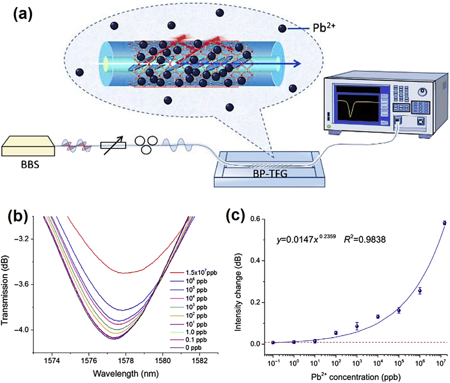 | ||
| Fig. 10 (a) Demonstration of the experimental arrangement for the detection of heavy metals, (b) transmission spectra of BP-TFG, showing a strong upshift with an increase in the concentration of Pb2+ ions, and (c) display of resonant intensity change versus Pb2+ concentration. Adapted with permission from ref. 269 Copyright 2018, Elsevier B.V. | ||
In the past few years, several 2D materials, including TMDCs, black phosphorus, and metal oxides, have been developed and utilized as channel materials to fabricate electrical sensors for the detection of various analytes. Accordingly, Zhang and colleagues presented the application of mechanically exfoliated MoS2 nanosheets as a channel material for the fabrication of FET devices for the detection of nitric oxide (NO).280 The absorption of NO on the n-type MoS2 surface resulting from p-type doping of the channel led to a decrease in current. The FET sensors based on multilayer MoS2 demonstrated a steady response compared to the unstable single-layer MoS2-based FET sensors and showed a detection limit of 0.8 ppm. Besides mechanically exfoliated MoS2, Zhang and colleagues demonstrated that MoS2 nanosheets exfoliated via Li intercalation-assisted method (solution-dispersed exfoliation technique) can be utilized as a channel for electronic sensors.165 The NO detection chemiresistor based on thin films of exfoliated MoS2 nanosheets showed an LOD of 190 ppt (parts per trillion).
Moreover, flexible NO2 gas sensors can also be fabricated by coating thin films of MoS2 nanosheets on flexible PET substrates, while rGO thin films can be utilized as flexible electrodes. Decorating the surface of the MoS2 thin films with Pt-NPs increased the sensitivity of the device and resulted in a lower LOD of 2 ppb toward NO2 detection. Jian Zhen et al. described a sensor for NO2 detection based on SnS2 flakes.281 The excellent selectivity of the proposed sensor towards NO2 arises from the robust affinity, appropriate position of partially occupied NO2 molecular orbitals, and Fermi-level of SnS2. This novel method can pave the way for the development of ultrasensitive and selective sensors for gas molecules based on 2D materials. Currently, various gas sensors have been developed using many 2D materials, including WS2,282,283 MoSe2,284 black phosphorus,285,286 WO3,287 ZnO,288,289 and NiO.290
Besides gas detection, MoS2-based sensors have also been developed to detect bio-analytes. Sarkar et al.291 reported the fabrication of MoS2-based biosensors, as presented in Fig. 11a and b. The device was fabricated on an SiO2/Si substrate (270 nm) with Ti/Au (60 nm/100 nm) as the metal contacts of the source and drain and the high-k dielectric (30–35 nm) HfO2 as the gate (Fig. 11d). In this method, the MoS2 flakes were obtained via a micromechanical exfoliation scheme (Fig. 11c); hence, the scalable synthesis of MoS2 can enable the scalable production of the proposed biosensing devices.
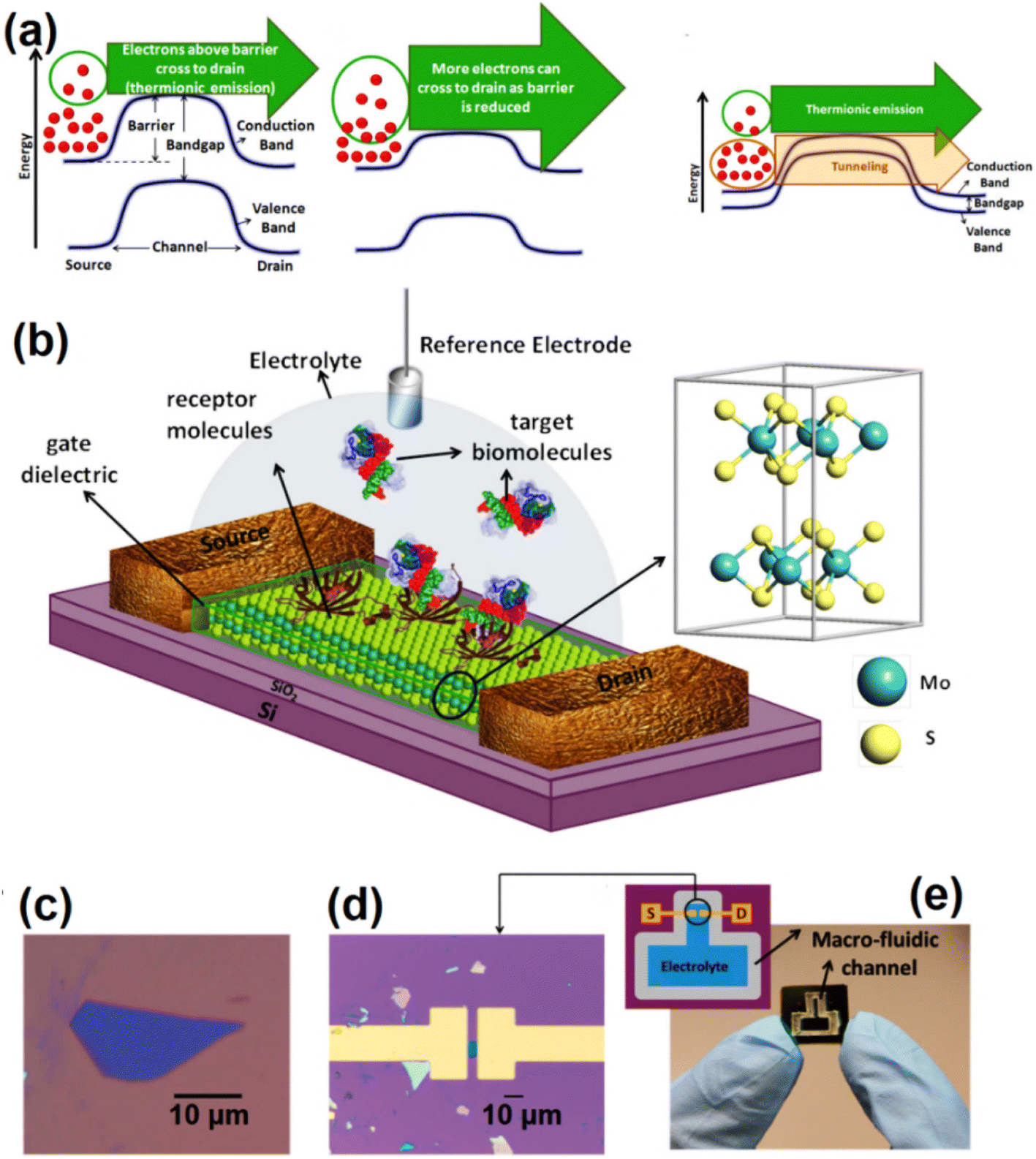 | ||
| Fig. 11 (a) Illustration of bandgap effects of graphene FET biosensor, (b) illustration of FET biosensors based on MoS2, (c) optical micrograph of MoS2 flake on SiO2/Si substrate and (d) optical micrograph for FET biosensor based on MoS2. (e) Image of a developed chip (inset represents its scheme). Adapted with permission from ref. 291 Copyright 2014, the American Chemical Society. | ||
Previous studies indicated that the direct contact of metal electrodes (source/drain) with electrolyte initiates the adsorption of biomolecules on electrodes, resulting in variations in work function of the metal and the contact resistance. In the study described above, a dielectric layer was used to passivate the source and drain contacts, overcoming the challenges faced in the previous study. The fabrication of fluidic channels for the storage of electrolytes was carried out via an acrylic sheet. For this purpose, an Ag/AgCl reference electrode (i.e., electrolyte gate) was utilized to apply a bias to the electrolyte, which is an essential factor in monitoring the working regime and achieving the stable operation of biosensors.291
Compared to graphene-based biosensors, semiconductor FETs work as a channel, where only electrons that possess energy greater than the source-to-channel barrier can pass from the source to drain (Fig. 11a). Therefore, lowering the barrier potential results in the larger movement of electrons to the drain. At the source, the energy occupied by the electronic levels is accessed by the Boltzmann distribution, and a final lower surface area is acquired at room temperature (60 mV dec−1). The small bandgap energy of the semiconducting material provides a considerably thin barrier, where the movement of electrons via direct tunneling can be attained even for low-energy electrons compared to barrier height (Fig. 11a).291 The FET sensor described above demonstrated outstanding sensitivity to both pH readings and biomolecule detection. In addition, MoS2-based FET detection devices can detect prostate-specific antigens, a potential biomarker for cancer.292,293 Moreover, the synthesis of new 2D materials is on an upward trajectory.194 Thus, it can be anticipated that additional electronic sensor devices can be constructed soon by exploiting novel 2D materials as channel materials to detect more target analytes. However, it is worth noting that although significant sensitivities have been achieved by utilizing 2D materials, they still have drawbacks. The low selectivity for specific target analytes arises from their great sensitivity to exogenous stimuli. In this case, altering the surface of channel 2D materials or sieving a thin layer covering has been mainly implemented to overcome this challenge. Specifically, due to their capacity to filter various gas molecules, which is selectively facilitated by their precise pore widths, MOFs are broadly employed as useful materials in gas separation.
Consequently, without compromising their sensitivity, it is expected that the sensitivity of FET sensors towards gas molecules can be improved significantly by depositing a thin MOF layer on the channel 2D material. The MOF layer can selectively sieve gas molecules with a diameter less than its pore size. A further method to increase the selectivity is modifying the surface of the channel with specific functional groups that enhance the interaction between the channel materials and the analyte, thus increasing the selectivity. Due to the surface oxidation and moisture absorption by these materials, electronic sensor devices based on 2D materials face drawbacks in terms of their short-term stabilities. Thus, to resolve this limitation, covering the channel with a stable thin layer material (e.g., metal oxides and polymers) has been proposed to shield the 2D materials from ambient conditions, resulting in increased stabilities.
| Material | Synthesis route | Sensing platform | Function | Analyte | LOD | Linear range | Ref. |
|---|---|---|---|---|---|---|---|
| Abbreviations: ULS = ultra sonication, NS = nano sheets, NA = nano assembly, MQDs = MXene quantum dots, GQDs = graphene quantum dots, CQDs = carbon quantum dots PEG = polyethylene glycol, PDA = polydopamine, QD-MB = quantum dot-molecular beacon, Aβ-o = amyloid-β oligomers, GFP = green fluorescent protein, FOX-7 = 1,1-diamino-2,2-dinitroethylene, LA = lipoic acid, TC = tetracycline, and AA = ascorbic Acid. | |||||||
| MoS2 | Hydrothermal | Apt-modified QDs & MoS2 | NSs as an energy acceptor | DA | 45 pM | 0.1–1000 nM | 319 |
| Hydrothermal | MoS2 MS/DNA/Si-Dot NA | FRET acceptor | Hg2+ | 0.86 nM | Up to 1000 nM | 320 | |
| Hydrothermal | MoS2 quantum dots | Fluorescent probe | Pb2+ | 50 μM | 33 μM to 8.0mM |
321 | |
| Hydrothermal | MoS2 QDs | Fluorescent probe | Fe3+ | 0.4 μmol L−1 | 5–50 μmol L−1 | 322 | |
| Hydrothermal | MoS2 NS/DNA | Fluorescent probe | Aβ-o | 3.1 nM | 0.01–20 μM | 323 | |
| Hydrothermal | MoS2/COOH | Fluorescent probe | Co2+ | 54.5 nM | Up to 1 μM | 324 | |
| MoS2/NH2 | Cd2+ | 99.6 nM | Up to 500 nM | ||||
| MoS2/SH QDs | Pb2+ | 0.84nM |
Up to 10 nM | ||||
| Hydrothermal | MoS2 QDs | Fluorescent probe | FOX-7 | 0.19 μM | 0.5–100 μM | 325 | |
| Solvothermal | MoS2 NS | DNA tagged MoS2 NS | miRNA-210 | 0.3 fM | 1 fM to 100 pM | 326 | |
| Li-intercalation | 2D-MoS2-GFP | Bioreceptor and quencher | Proteins | 1 nM | 0.5–50 nM | 327 | |
| Liquid phase exfoliation | CQDs/MoS2 | Fluorescent probe | Bisphenol S | 2 nM | 0.05–2 μM | 328 | |
| ULS Li-intercalation | MoS2@PDA-PEG-peptide | MoS2 NS as acceptor | Saspase-3 | 0.33 ng mL−1 | 2–360 ng mL−1 | 329 | |
| — | QD-MB@MoS2 | Fluorescent probe | miRNA-155 | 7.19 fM | 1 nm to 10 fm | 330 | |
| miRNA-150 | 5.84 fM | ||||||
| — | MoS2 NS | MoS2 – fluorescent quencher | AFM1 | 0.5 nM | 0.7–10 nM | 331 | |
| (FAM-CS) – fluorescent probe | |||||||
| WS2 | Hydrothermal | WS2 QDs | “Turn-on” fluorescent sensor | LA | 0.59 μM | 1–10 μM | 332 |
| Hydrothermal | Blue fluorescent WS2-QDs | Stable fluorescence | Fe3+ | 1.32 μM | 0–55 μM | 333 | |
| — | WS2-Pt-Fe2O3 | Strong adsorption | Lipopolysaccharide | 0.12 nM | 4–1000000 ng mL−1 |
334 | |
| Encapsulation of micromotors | |||||||
| — | WS2 NS | Fluorescent probe | Hg2+ | 0.1 nM | 0.5–20 nM | 335 | |
| — | WS2 NS | Fluorescence probe | Hg2+ | 3.3 nm | 5–500.0 nM | 336 | |
| Ag+ | 1.2 nM | ||||||
| Graphene | Hydrothermal | S,N-GQDs | Photostability | AA | 1.2 μM | 10–500 μM | 337 |
| Hydrothermal | N-GQDs | Photostability | Hg2+ | 23 nM | 0–4.31 μM | 338 | |
| N-GQDs/Hg2+ | Tuneable luminescence | Paraquat | 19 μg L−1 | 0.05–2.0 μg mL−1 | |||
| Hydrothermal | B, N-GQDs | Photostability | Hg2+ | 6.4 nM | 0.2–1 μM | 339 | |
| MXenes | Hydrothermal | N-doped Ti3C2 QDs | Enhanced fluorescence of MQDs | Fe3+ | 0.17 μM | 0.5–500 μM | 340 |
| Cu2+ | 0.15 μM | ||||||
| Hydrothermal | Ti3C2 NS | Up-conversion luminescence of Ti3C2 | L-Tryptophan | 91 nM | 0–5 μM | 341 | |
| Solvothermal | N-Ti3C2 MQDs | Fluorescent probe | Cr(VI) | 0.012–0.02 μM | 0.1–500.0 μM | 342 | |
| AA | |||||||
| Hydrothermal | N,B-Ti3C2 MQDs | Wavelength-dependent blue PL | TC | 20 nM | — | 343 | |
| Hydrothermal | N-Ti3C2 MQDs | Fluorescent probe | Glutathione | 0.17 μM | 0.5–100 μM | 344 | |
| Microwave-assisted | N,P-Ti3C2 MQDs | Fluorescent probe | NO2− | 0.71 μM | 0–80 μM | 345 | |
| Hydrothermal | N-doped Ta4C3 MQDs | Fluorescent probe | Fe3+ | 2 μmol L−1 | — | 346 | |
| Hydrothermal | Ti3C2 MQDs | Fluorescent probe | Fe3+ | 1.4 μM | 1.4 μM to 0.8 mM | 347 | |
However, Shijiang et al. significantly modified the architecture of GO-based fluorescence sensors.295 Considering the ability of GO to differentiate ssDNA and dsDNA, dye-labeled ssDNA-hybridized GO sheets were immobilized with target DNA. Compared to previous studies, the sensor showed great selectivity and sensitivity for the detection of DNA with an LOD of 100 pM. This work also demonstrated the feasibility of the multiplex detection of DNA against different DNA targets as interfering agents. Subsequently, fluorescence sensors were developed using GO nanosheets as a detection platform to detect a variety of analytes, such as proteins, small molecules, nucleic acids, and metallic ions, with enhanced selectivity and sensitivity.296,297 Due to the exceptional performance of GO-based fluorescence sensors and based on the ability of MoS2 to distinguish ssDNA and dsDNA (double-stranded DNA), sensors were fabricated based on various fundamental ideas similar to that presented by Fan and coworkers.295 The resulting sensor demonstrated excellent DNA detection selectivity and sensitivity with an LOD as low as 500 pM (Fig. 12).25 Subsequently, Zhang and colleagues published a comprehensive review and compared monolayer MoS2, TaS2, and TiS2 fluorescence sensing platforms for DNA recognition.298 They showed that under similar conditions, TaS2-based sensors have better performance with enhanced sensitivity and lower LOD (0.05 nM) compared to that composed of MoS2 (0.1 nM) and TiS2 (0.2 nM). In addition, a monolayer-based TaS2 fluorescence sensor has been proposed for the multiplex detection of DNA.
 | ||
| Fig. 12 (a) Graphical illustration of fluorescent DNA sensor based on MoS2 (single-layer), (b) fluorescence spectra of (i) FAM-labeled ssDNA probe (P1) and P1/T1 duplex (ii) without MoS2 (iii) with MoS2, (c) fluorescence spectra of P1 using different T1 concentrations and (d) calibration curve for DNA sensing. Adapted with permission from ref. 25 Copyright 2013, the American Chemical Society. | ||
Furthermore, many fluorescent sensors have been produced based on extremely thin 2D materials, including MoS2,299,300 WS2,301,302 Ta2NiS5,303 g-C3N4,304,305 and MnO53,306 for targeted and accurate detection towards a range of target species, e.g., DNA, proteins, metal ions, and tiny molecules. Besides 2D inorganic materials, Peng et al. extended the notion of fluorescence sensor fabrication using organic–inorganic 2D MOF nanosheets.307 Similar to graphene and TMDCs, it has been shown that 2D MOF nanosheets have good quenching capability for probing DNA and can be utilized for the fabrication of fluorescence platforms for DNA sensing. 2D MOF-based sensors (2D Cu-TCPP nanosheet-based) demonstrated superior selectivity and sensitivity with an LOD of 20 pM. In contrast, fluorescent sensors can be expanded to other novel 2D materials, e.g., COFs, MXenes, black phosphorus, and polymers. Specifically, fluorescence sensors based on 2D materials provide several benefits. Firstly, all the fluorescence sensors described above rely on solution-processed 2D materials, which are cost-effective and offer scalable production. In addition, fluorescence sensors provide a relatively quick and straightforward detection method, with a response that only takes a few minutes. The same solution can also be employed to detect a wide range of target analytes. Lastly, 2D material-based fluorescent sensors tend to be more sensitive compared to various other types of fluorescent sensors due to the greater fluorescence quenching efficiency conferred by their 2D structural features. Conversely, fluorescence sensors have several shortcomings. In particular, due to the complicated production of dye-labeled ssDNAs and/or probe DNAs, the resultant fluorescence sensors are extremely expensive. Moreover, the limited stability of fluorescent dyes attached to DNA further limits the life of fluorescent sensors.66
For example, a 3D hybrid MoS2/AgNPs/inverted pyramid polymethyl methacrylate (IPPMMA) flexible SERS sensor,311 mounted at the edge of an optical fiber (Fig. 13a and b), could achieve the remote detection of complex analytes. Each analyte molecule could be easily distinguished based on their specific Raman peaks (Fig. 13c). MoS2 can be used as a protective layer through liquid and atmospheric conditions, indicating its benefits for real-life biosensing applications. Compared to lab research, flexible SERS substrate sensitivity with outstanding performance is still a significant problem for real-world applications. AgNPs@MoS2/pyramidal polymer (polymethyl methacrylate), a 3D flexible plasmonic structure, has a large surface area and can produce dense 3D plasmonic hot spots (Fig. 13d).312 A standard melamine solution (Fig. 13e) and melamine and milk mixed solution (Fig. 13e) with a concentration of 10−10 to 10−4 M and 10−6 to 10−3 M, respectively, are utilized to corroborate the SERS efficiency of the flexible substrate. The 3D AgNs@MoS2 activated surface was housed on the prepared solution surface solution (Fig. 13e) for in situ detection. The characteristic peaks of MoS2 and melamine could be examined with an ultralow LOD of 10−10 M (Fig. 13f). Furthermore, one of the unique advantages of flexible SERS sensors is their ability to couple precisely with arbitrary surfaces, realizing in situ on-site sensing. For instance, using a micro-current-assisted chemical reduction procedure and an easy etching process, Qiu et al. described the use of PMMA-supported monolayer graphene with sandwiched Ag-nanoflowers (G/AgNFs/PMMA) as a flexible SERS substrate (Fig. 13g). Coating the substrate on the surfaces of real-world materials, such as phenylalanine@apple (Fig. 13h), methylene-blue@fish (Fig. 13i), and aqueous adenosine solution, produced distinct Raman signals. Therefore, it is suitable for the detection of arbitrary morphological or aqueous solution surfaces.313 Furthermore, controlling LSPRs to produce high-density local hot spots and significant SERS amplification requires certain nanogaps. Nevertheless, creating 3D ultra-narrow nanogaps for practical applications is a considerable impediment. Li and coworkers described a gyrus-inspired Ag nanostructure designed on graphene/Au films for SERS.314 The 3D ultra-narrow nano-gaps (∼3 nm) were obtained between Ag-gyrus using the width of ∼22 nm. This flexible SERS substrate was applied to detect malachite green residue (10–11 M) on prawn skin for in situ application. Convincingly, SERS platforms with flexible 2D materials can be perceptually integrated into point-of-care diagnostics using handheld Raman spectroscopy and smartphone expertise.308
 | ||
| Fig. 13 (a) Photograph of remote detecting mixed molecules. (b) Schematic of the partially enlarged detail on the interface between the MoS2/AgNPs/iPPMMA flexible SERS substrate and the probe solution. (c) SERS spectra of R6G (10−10 M, black line), Sudan red I (10−6 M, red line), Congo red (10−6 M, pink line), malachite green (10−7 M, blue line) and their mixtures (green line). Adapted with permission from ref. 315 Copyright 2018, Elsevier B.V. (d) Schematic of the 3D flexible AgNPs@MoS2/pyramidal polymer substrate preparation process. (e) Standard melamine solution and (f) SERS spectra of the standard melamine solution with a concentration ranging from 10−10 to 10−4 M. Adapted with permission from ref. 312 Copyright 2018, John Wiley & Sons, Ltd. (g) SEM images and schematic of the G/AgNFs/PMMA flexible SERS substrate. (h) SERS detection on an apple surface with adsorbed phenylalanine molecules. (i) SERS detection on a fish surface with adsorbed methylene-blue molecules. Adapted with permission from ref. 313 Copyright 2017, Elsevier B.V. | ||
3.4.5.1 Fine structure characterization. Compared to their 3D counterparts, 2D materials possess a variety of exceptional electrical, optical, physical, and chemical properties due to their fine architectures, including the number of layers, edge structure, and defects. Consequently, studying these essential structural differences is crucial for modifying 2D materials and their future applications. Raman spectroscopy is an effective tool for probing the microstructure of 2D materials.316,317 However, the Raman signals from graphene are typically weak, given that they contain a low fraction of scattered radiation, making it challenging to distinguish fine structural properties such as low defect concentration, functional groups, and edge structures. In this case, using the interference-enhanced Raman scattering (IERS) technique,318 an enhancement ratio of 30 was obtained for graphene. SERS is another spectroscopic technique with high spatial resolution, ultrasensitive detection limits, and great structural selectivity. Therefore, the surface and interference co-enhanced Raman scattering (SICERS) method can achieve a 10 to 102 times greater enhancement ratio than IERS or SERS alone using a specially designed substrate of active metal layer/Si oxide/SERS. Furthermore, surface variations and small structural changes in graphene can also be detected. Moreover, some fragments or ribbons on the irregular surface of graphene can be observed through AFM imaging of the material on the IERS and SICERS substrates. In the Raman spectra of graphene on an SICERS substrate obtained with low laser power, two additional peaks can be correctly identified due to the vibrations of the fragments or ribbons on the surface of graphene. This method makes SERS a more effective tool for characterizing ultra-sensitive structures in 2D material-based nanoelectronics.
3.5 Human chemical signal monitoring
The human body produces chemical signals, another type of information vital for personalized healthcare, illness detection, and evaluation. Typically, chemical sensors are composed of two components, i.e., a receptor and type of physicochemical signal transducer. The role of the receptor is to offer better selectivity towards specific biomarkers, whereas the function of the transducer is to turn the chemical information into a quantifiable signal that can be analyzed. By virtue of their large surface area and ease of surface modification, 2D materials exhibit incredible potential to detect human chemical information. Furthermore, chemical sensors based on 2D materials are commonly employed for the non-invasive, cost-effective, and continuous evaluation of different analytical concentrations.39 They can further be categorized depending on the site where chemical signals are generated, e.g., it can be employed for breath monitoring, sweat, and saliva detection.Zhang et al. examined different concentrations of Ca2+, K+, and Na+ ions using self-assembled graphene-based ion-sensitive sensor arrays (Fig. 14a).355 To ensure the interaction of compatible ions with the active materials, various ionophores were decorated on each sensing region; hence, the conductance of the graphene layer was altered with each ion absorption array. It is worth noting that the graphene sensor exhibited a considerably lower detection limit than the carbon nanotube sensor. Besides, the observation of a small  noise in the samples based on graphene was unexpected. This sensor responded quickly and had a minimal LOD for diluted human perspiration in the range of 0.1–100% (Fig. 14b); consequently, the ion sensor array was proven to be beneficial for evaluating sweat ions in human healthcare. This is different from conventional sweat testing, which has the drawbacks of being time-consuming and requiring a significant sample size. Xu et al. demonstrated the chromogenic response of a graphene-coupled inverse opal cellulose film to measure the sodium chloride content in sweat as an alternative.352 It is possible to utilize the reflection spectra of the biosensor to measure body dryness during exercise given that its reflection spectrum redshifted with an increase in the concentration of the sample. As a result of the dramatic color change and diffraction-peak shift, it was quite easy to differentiate the NaCl content in this solution. Due to the strong relationship between the glucose content in sweat and the corresponding level in the blood, glucose is a diabetic biomarker that can be determined through sweat.348 In the case of diabetes control, glucose concentration is critical. Accordingly, wearable glucose sensors with non-invasive, convenient, and real-time detection capabilities must be urgently developed. Based on rGO nanocomposite electrodes, wearable electrochemical glucose sensors were developed by Xuan et al. to measure the blood glucose levels.356 The working electrode as composed of Au/rGO/AuPt NPs and its surface was coated with Nafion, and subsequently immobilized with GOx (Fig. 14c). The redox ability of GOx catalyzed/oxidized glucose to gluconolactone and hydrogen peroxide. During this event, the current is related to the glucose content and via amperometric measurements (i vs. t), the redox potential was used to quantify the generation of H2O2 on the working electrode surface.
 | ||
| Fig. 14 (a) Representation of ion-sensitive sensor constructed on self-assembled graphene for ion collection and (b) variations in the sensor resistance at various concentrations (i.e., NaCl, and human sweat). Adapted with permission from ref. 355 Copyright 2012, Elsevier B.V. (c) Illustration of rGO-based wearable sweat glucose biosensor with a digital photograph of glucose biosensor on the wrist. Adapted with permission from ref. 356 Copyright 2018, Elsevier B.V. (d) Application of graphene-hybrid based electrochemical prototype on the human skin and (e) analysis of glucose levels in human sweat and blood over a day. Adapted with permission from ref. 357 Copyright 2016, Nature Publishing Group. (f) Digital photographs of transdermal observation of cortisol using MoS2-based biosensor in human sweat. (g) Lab potentiostat and portable assessment of |Z| cortisol reaction in sweat for 3 h observation. Adapted with permission from ref. 360 Copyright 2017, Nature Publishing Group. | ||
In addition, a waterproof band was used to laminate the sensor to the surface of the skin to support sweat collection. The sensor demonstrated good efficiency and showed a tendency for glucose detection in human perspiration with a short reaction time of 12 s and sensitivity of 82 A mM−1 cm−2 in the concentration range of 0.1–2.3 10−3 M.39 Recently, Lee et al. reported the fabrication of graphene-based multifunctional devices for the continuous assessment and treatment of diabetes.357 Graphene doped with gold offers excellent conductivity, mechanical robustness, and optical luminosity to provide constant electrical signal transfer. This is useful for electrochemical activity and biological sensitivity and selectivity. Using the diabetes route in human sweat, researchers could perform in vivo glucose monitoring (Fig. 14d and e). The detected glucose concentration was consistent when compared with a commercial blood glucose sensor. Upon heating phase-change substances, the formed microneedles can be used as a medication container to release active pharmaceutical ingredients. A potential method for the treatment of the chronic diabetes mellitus is using a conformal integrated device. However, for large-scale applications, complex fabrication techniques are not suitable. Researchers have also worked on the development of graphene-based disposable glucose biosensors.358,359 Direct laser engraved graphene sensors, which can be manufactured using three easy procedures and utilized for scalable production (see Fig. 14f and g), are particularly suitable for these applications.360 The charge distribution on the surface of the MoS2 semiconductor may be altered by the target molecules bound to it, resulting in a change in capacitive reactance and/or impedance. Kinnamon et al. employed MoS2 nanosheets modified with cortisol antibodies in human perspiration for cortisol monitoring based on a similar concept.360 Through impedance measurements, the sensor showed an LOD of 1 ng mL−1 with a dynamic range of 1–500 ng mL−1. A portable device to detect cortisol concentrations in sweat has also been produced, demonstrating a performance equivalent to that of a laboratory potentiometer. It is possible to use graphene and MoS2 together to create a composite that can be utilized for glucose and lactate sensing.239 Fast reaction, strong selectivity, excellent repeatability, and flexibility make it a promising candidate for glucose and lactate determination in sweat. Besides TMDCs, MXenes offer enormous potential in various applications for glucose monitoring. Rakhi et al. prepared gold nanocluster-decorated Ti3C2Tx sheets (Au@Ti3C2Tx-MXene nanocomposites) and immobilized them with GOx for glucose detection.361 The proposed sensor (GCE/Nafion-u@Ti3C2Tx/GOx) showed an LOD of 5.9 × 10⁶ M with a concentration range of 0.1–18 mM and exhibited a sensitivity of 4.2 μA mM−1 cm−2. Therefore, it is possible to use MXenes and the proposed sensors for the electrochemical measurement of glucose in human sweat, as well as for other applications.
 | ||
| Fig. 15 (a) Illustration of breathing humidity observation using flexible biosensor at different breathing frequencies. Adapted with permission from ref. 364 Copyright 2018, Elsevier B.V. (b) Image of GO-based humidity sensor with signals recorded from breathing and speaking, Adapted with permission from ref. 362 Copyright 2013, the American Chemical Society. (c) SEM micrograph of a fiber humidity sensor based on MoS2. Adapted with permission from ref. 371 Copyright 2017, Elsevier B.V. (d) Illustration of ssDNA-functionalized graphene-based sensor and PCA. Adapted with permission from ref. 366 Copyright 2017, John Wiley & Sons. (e) Pictorial representation of MoS2-based detecting mechanism with target VOC molecules. Adapted with permission from ref. 379 Copyright 2014, the American Chemical Society. (f) Representation of 1T-WS2 nanosheet-based biosensor together with its selectivity behavior (for H2O and methanol sensing). Adapted with permission from ref. 380 Copyright 2015, John Wiley & Sons Copyright 2015. (g) Demonstration of Ti3C2Tx-based gas sensor. Adapted with permission from ref. 388 Copyright 2018, the American Chemical Society. | ||
It is possible to monitor changes in humidity during breathing when sensors are mounted on a medical mask. Together with the symptoms of apnea and blocked breathing rhythm, they can also distinguish between rapid, regular, and deep breathing. Moreover, humidity sensors can document dehydration before and after water intake, which can benefit patients with speech impairments. GO layers provide hydrophilic properties, which allow water molecules to adhere to the surface and change the electrical characteristics of the humidity sensor. Borini et al. demonstrated a rapid response to moisture by using an ultra-thin GO film on an interdigital electrode.362 Due to its flexibility, transparency, and large-scale production capacity, GO can be effectively used in a humid environment (Fig. 15b). The response and recovery time were affected by thickness, e.g., a 15 nm-thick film had an average response time of 30 milliseconds. It was used successfully to record subtle notes of human speech and respiration in real time. Various whistled tunes could be classified and distinguished with greater than 90% accuracy using principal component analysis (PCA) and fast Fourier transform, suggesting that this approach is a valuable validation method. A similar non-contact technique was used by the rGO-based humidity sensor, which could acquire information on humidity fluctuations in real time and analyze psychological symbols in the human body.370 Du et al. prepared an etched single-mode fiber (ESMF) humidity sensor with MoS2 coating, possessing a diameter of 18 μm and length of ∼15 mm (Fig. 15c).371 The optical frequency conductivity of the MoS2 sheets varied in response to changes in RH due to the synergistic effects between the MoS2 and the evanescent field, which resulted in variations in the power of transmitting light.
Regarding the human breath, the MoS2-coated ESMF showed a considerable rise in transmitting light power up to 14 times compared to the naked ESMF, together with a rapid response (0.066 s) and rapid recovery rate of 2.395 s. The hybridization of MoS2 with Ag NPs,372 SnO2,373 Cu2S,374 and graphene375 has been extensively investigated to improve the sensitivity, detection limit, and response time. When Ag NPs were used to modify the surface of MoS2, all the essential parameters showed a significant improvement compared to the pristine MoS2.372 It is probable to detect variations in humidity during respiration at various breathing frequencies and during speech. A disposable cellulose-paper-based humidity sensor was developed to measure humidity, temperature, breath quality, and ethanol adulteration, which was also equipped with a portable circuit.374 The MoS2/Cu2S hybrid worked as the active sensing material when used in the flexible and wearable multifunctional system. Several researchers, including Muckley et al., recently investigated the humidity performance of Ti3C2 films, a member of the MXene family.376 MXenes can also be used for respiration monitoring due to their reversible response in the RH range of 0.1% to 95% with an LOD of 20 mTorr H2O partial pressure with <0.1% RH. Because exhaled breath contains more than 1000 volatile organic chemicals and is strongly humidified (>80%), including carbon monoxide, acetone, hydrogen sulfide, and ammonia, it is imperative to realize a high-efficiency analyzer with substantial selectivity and a detection limit down to the ppb level in complicated gas mixtures.377,378 Jung et al. proposed sensors in which ssDNA solution was utilized to make the graphene layers more suitable to improve the selectivity and sensitivity (Fig. 15d).366 Graphene modified by ssDNA also served as an additional sensing channel, which increased the signal processing under intense humidity conditions by increasing the carrier density. A response intensity of 98.5% was observed towards 2 ppm H2S vapor with an exceptionally low LOD of 0.0053% in RH of 80%. PCA analysis demonstrated that the ssDNA-graphene sensor array can discriminate halitosis and kidney-disordered cancer-related biomarkers, H2S, NH3 biomarkers, and other VOCs such as CO, CH3COCH3, C2H5OH, and C7H14O. Thus, this demonstrates a valid detection network that is inexpensive and a non-invasive diagnosis method to monitor exhaled gases. Wang et al. studied diabetes-related acetone detection in high humidity (85%).367 For the detection of NO2, it is possible to obtain rapid reaction and recovery time by including a heater inside the gas sensor made of graphene.377 This is particularly interesting because multiple functionalized rGO can monitor physiological signals and VOCs simultaneously without interfering with the transmission of signals,378 which can broaden the scope of its application in preventative medicine. For example, TMDCs such as MoS2,379 WS2,380 and their hybrids381,382 display extraordinary semiconducting characteristics, with bandgaps that are adjustable based on thickness and doping molecules used in their fabrication. Thus, TMDCs have the potential to be used in the manufacture of gas sensors. The theoretical analysis results indicated that NO can significantly alter the bandgap and electron transmission of MoS2,383 which was also corroborated by the experimental findings.55
In addition, the MUA (mercaptoundecanoic acid)-conjugated MoS2 films produced by Kim et al. were used as tunable VOC sensors with variable response times.379 VOC molecules were physisorbed on sensing channels due to dipole-induced scattering (Fig. 15e) and were responsible for rapid reactions with toluene and hexane vapors (Fig. 15a and b). In addition to providing high-energy binding sites for VOCs, the MUA-MoS2 coating prevented them from attaching directly to the surface of MoS2. Therefore, it showed greater resistance fluctuation compared to MoS2. Further, the sensor showed a high sensitivity and a lower LOD of 1 ppm, which suggest the use of breath analysis in lung cancer diagnosis in the near future. Mayorga Martinez et al. investigated the selective gas performance of 1T-WS2 in their study.380 Methanol and water could be separated using impedance spectroscopy because of the impedance phase difference between them (Fig. 15f). This device has potential to be employed as a dependable, sensitive, and repeatable instrument for onsite gas sensing applications, particularly in the case of inhaling complex gas mixtures that are present in the environment. Besides graphene and the family of TMDCs, the exceptional surface chemistry of MXenes and their excellent conducting nature and biocompatibility make them an extremely appropriate matrix for improved biological sensing systems, together with other applications.384–386 MXene materials utilized in solid-state gas sensors presented minimal electrical noise, excellent signal efficiency, adaptable fabrication, and portability. They have been proven to be successful in detecting various gas molecules with good signal strength, versatility, and accessibility. Yu et al. reported first-principle calculations to theoretically anticipate the potential use of MXenes in the field of gas sensing.384 They observed that the oxygen-terminated Ti2C single layer (Ti3C2Ox) is incredibly selective to ammonia compared with other gas molecules, including NO2, CH4, O2, and N2. Lee387 and Yuan et al.385 further confirmed that Ti3C2 gas has excellent resistance towards ethanol (C2H6O), methanol (CH3OH), acetone (CH3)2CO, and ammonia (NH3). Ti3C2Tx displays both minimal signal noise and robust signal processing for VOCs, as proven recently by Kim et al.388 Filtration of a diluted colloidal Ti3C2Tx MXene layer AAO membrane resulted in the formation of an MXene film, which was subsequently transferred to an SiO2 wafer printed with gold-sensing electrodes (Fig. 15g). Acetone, ethanol, ammonia, and propanol were detected with strong response signals from MXene-based gas sensors, but NO2, SO2, and CO2 were detected with a considerably lower response, suggesting superior selective detection for VOCs in the gas sensor. Furthermore, MXenes have great potential in gas sensing with ultrahigh signal/noise ratio in contrast with their 2D counterparts such as MoS2, black phosphorus, and rGO.
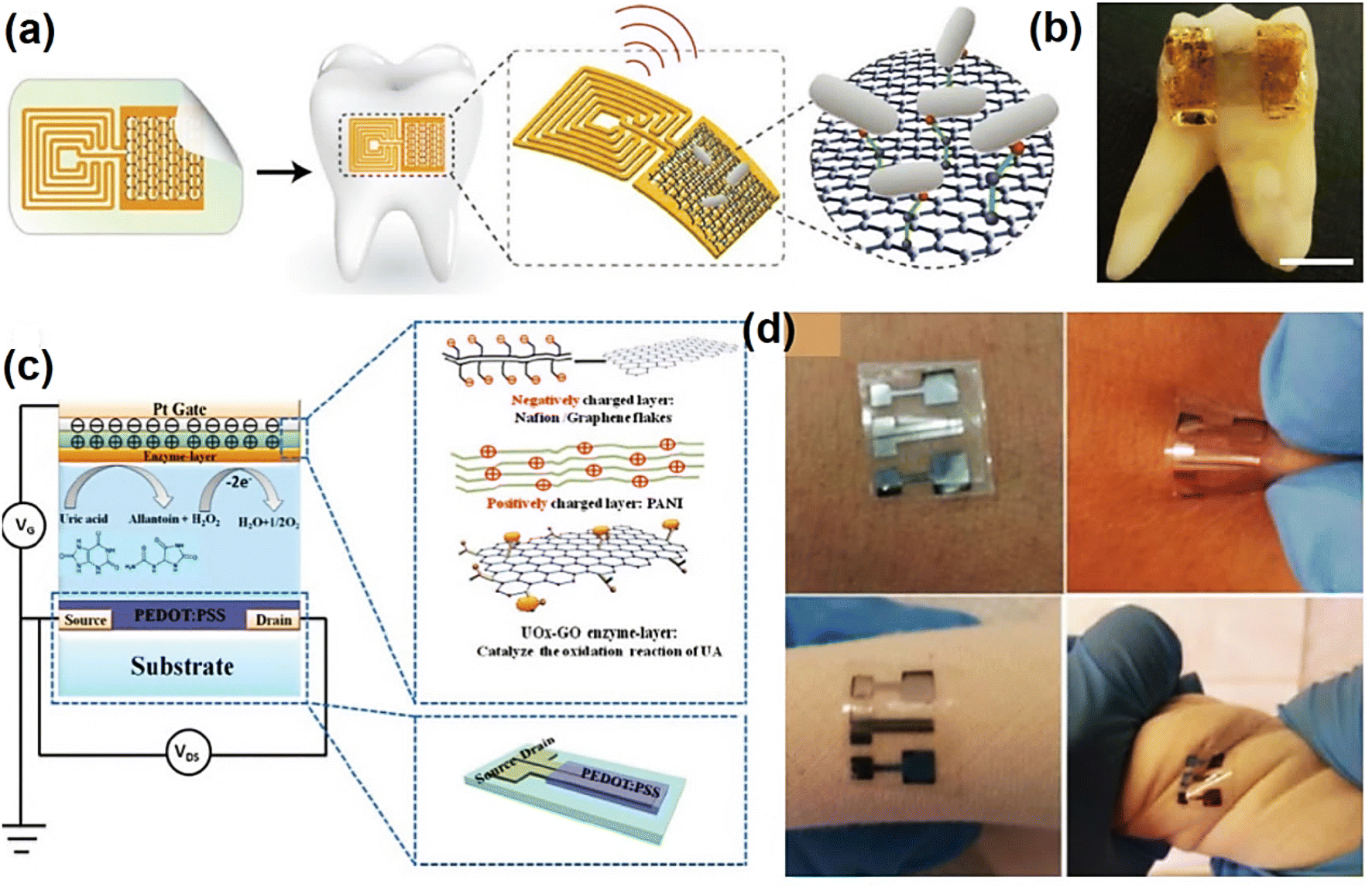 | ||
| Fig. 16 (a) Graphical representation of graphene/silk-based wireless biosensor (mounted on a tooth) for sensing bacteria. (b) Digital photograph of the developed sensor (over tooth surface). Adapted with permission from ref. 392 Copyright 2012, Nature Publishing Group. (c) Schematic of the working mechanism and organic electrochemical transistor with Pt-gate/Nafion-graphene/PANI/UOx-GO employed for saliva analysis. (d) Application of proposed sensors on various surfaces. Adapted with permission from ref. 393 Copyright 2015, John Wiley & Sons. | ||
Furthermore, biosensors have been successfully used for the instantaneous monitoring of glucose and uric acid concentrations in saliva, implying that they represent potential technology for the non-invasive detection of saliva biomarkers. From an application point of view, wearable electronics made from 2D materials are designed to detect sweat, saliva, and breathing gases. Based on this, the graphene family is the most often utilized active material in both applications. However, due to their limited selectivity, the detection of some VOCs during respiration remains a significant obstacle, despite various demonstrations for their practical use, such as sensing the moisture in respiration, detecting electrolytes in sweat, and determining glucose in sweat. Another critical problem that requires attention is the low levels of specific biomarkers in VOCs. For practical applications, the LOD and selectivity of chemical sensors based on 2D materials need to be enhanced. Their efficacy can be optimized by considering their rich chemical environment and signal processing efficiency.
3.6 Biomedical and health care sensors
 | ||
| Fig. 17 Schematic of optical prism coated with graphene for the ultra-sensitive low detection of distinct cells (a typical SPR system): (a) flow-detecting structure for a single-cell setup, and the inset corresponds to optical sensor platform with graphene-coated for single cell detection, (b) distinct voltage change (time-dependent) agreeing with mixed Jurkat cells and lymphocytes due to their rolling through h-rGO sensing frame and (c) enlarged image of certain positions of the panel (voltage signals are clearly described). Microscopic image (15 μm scale bar) of (d) Jurkat cells and (e) lymphocytes. Adapted with permission from ref. 394 Copyright 2014, the American Chemical Society. | ||
Further, the size and refractive index of JCCs are considerably higher compared to ordinary lymphocyte cells. Discrete fluctuations in voltage signal (considering amplitude) with time were observed, as displayed in Fig. 17b, which revealed the flow of normal lymphocytes and JCCs at a 7 μL h−1 approximate rate via the h-rGO-based optical microfluidic channel. Additionally, the high and low-voltage signals, as presented in Fig. 17c, agree with the presence of JCCs and normal lymphocyte, signifying superior sensitivity and resolution of GOPS. Consequently, even a single cancer cell could be identified from the neighboring healthy cells. The microscopy images are shown in Fig. 17d and e, where the JCCs (Fig. 17d) are typically bigger compared to normal lymphocyte cells (Fig. 17e). The average refractive index of cells refers to the average size of normal and cancerous cells, which can be precisely identified through an optical refractive index sensor based on graphene.394
It also operates as a biocompatible interface layer, allowing DNA molecules to be hosted on its surface. Fig. 18a depicts a schematic layout of the PL experiment that was employed for ultrasensitive DNA detection hybridization via the proposed hetero-structure device. The PL spectrum obtained following the interaction of DNA molecules was investigated via confocal microscopy. The spatial PL area mapping for the DNA solution immobilized on the proposed hetero-structural sensing substrate (40 L; 10 M) is shown in Fig. 18b. Furthermore, the sensing substrate was hybridized with the corresponding DNA solutions (different dilutions from 1 to 100 aM). As more target DNA was immobilized on the substrate, the PL mapping intensity increased proportionally. The sensing substrate was rinsed with ultra-pure water and dried after each incubation of probe and target DNA, and PL measurements were carried out under dry conditions. The integrated PL peak area was corelated with the target DNA in the concentration range of 1 aM to 1 fM, as depicted in Fig. 18c, recorded in the range of 1.7–1.95 eV for each condition. The results of the PL color mapping show that the graphene/MoS2 heterostructure sensing substrate determined the target DNA in a low concentration down to the aM level.
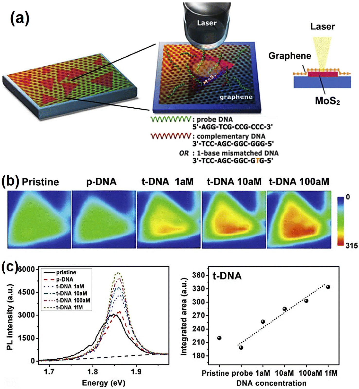 | ||
| Fig. 18 (a) Representation of DNA sensing strategy using graphene/MoS2 heterostructure sensor and an optical microscope, (b) mappings of PL peaks of target DNA-hybridized heterostructure sensing substrate, and (c) PL spectra and integrated PL peak of target DNA-hybridized heterostructure sensing substrate. Adapted with permission from ref. 395 Copyright 2014, John Wiley & Sons. | ||
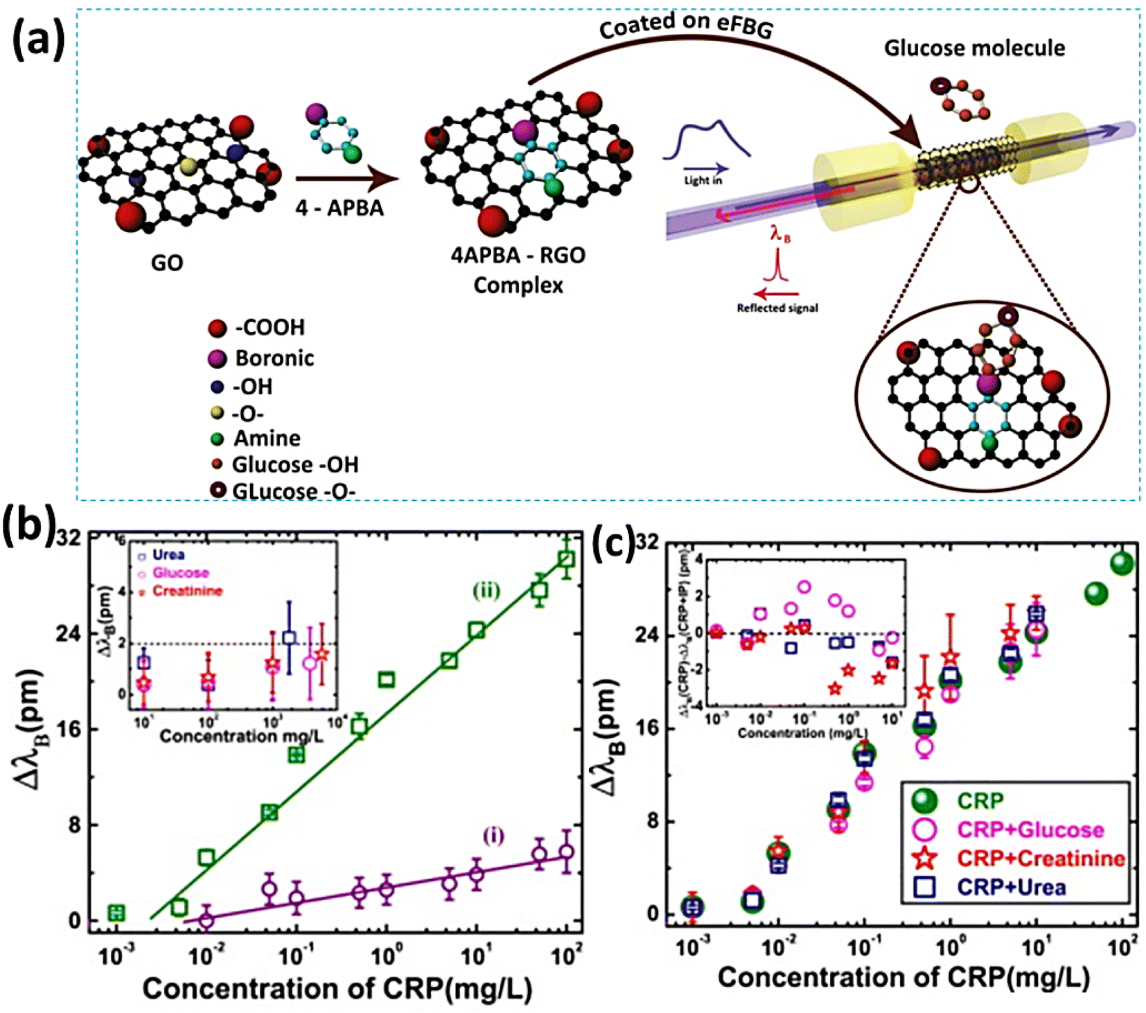 | ||
| Fig. 19 (a) Graphical representation of eFBG sensor layered through aminophenyl boronic acid-rGO complex for glucose detecting mechanism. Adapted with permission from ref. 397 Copyright 2016, John Wiley & Sons. (b) Shifted Bragg's wavelength for different CRP concentrations in the case of (i) aCRP and (ii) aCRP-GO complex-coated eFBG sensors (inset corresponds to shifted Bragg's wavelength concerning interfering concentration, for example, magenta color for glucose, blue for urea and red for creatinine), and (c) shifted Bragg's wavelength for a concentration of CRP in the presence of creatinine (5800 mg L−1), glucose (3800 mg L−1), and urea (1800 mg L−1) (inset represents modification in ΔλB aimed at different concentrations of CRP with respect to various concentrations of CRP in the presence of contrast agent, e.g., creatinine, glucose, and urea). Adapted with permission from ref. 396 Copyright 2015, Elsevier B.V. | ||
Consequently, it is critical to develop precise and cost-efficient cancer detection methods, and subsequent treatment techniques. Recently, graphene and its derivatives, as well as other nanomaterials, have made new techniques conceivable in the field of biosensors.398 The various properties of graphene and graphene-quantum dots make them attractive candidates for use as fluorescence probes in phase contrast imaging (PL imaging). Fluorescence-based biosensors should be biocompatible, photostable, non-toxic, and chemically inert, and hence these factors must be considered during the fabrication of these devices. Graphene-based fluorescent probes for PL have two critical functions, as follow: (i) they can identify cancer cells with high specificity and (ii) they can also be used to deliver therapeutic drugs. Cancer tumors have been successfully treated and cured with light-induced thermal treatment in clinical trials. During photothermal treatment, near-infrared (NIR) light penetrates only a limited depth in the target human tissues, allowing medications to be delivered safely. Alternatively, the use of phototherapy alone may result in the partial destruction of cancer cells.
In this case, photothermal therapy combined with chemotherapy is a more effective therapeutic option than either treatment alone. When combined with photothermal therapy, chemotherapy can increase the effectiveness of the cancer treatment by targeting cells and blocking the regeneration of impaired (tumor-affected) blood vessels. Recent developments include the development of light-illuminated NPs, which discharge their payload in response to light activation, resulting in increased bioavailability, while maintaining high efficiency.398,399 Recently, Liu et al. achieved excellent drug delivery to cancer cells by combining photothermal and chemotherapeutic targeting of cancer cells using PEGylated 2D MoS2 nanosheets.398 The IR absorption of 2D MoS2-PEG (polyethylene glycol) nanosheets is extremely strong, making them suitable for photothermal treatment. Nanosheets possess a high surface/mass ratio, which allows an active loading of medicinal compounds, i.e., chemotherapeutic medications doxorubicin (DOX) and photodynamic agent chlorine e6 (Ce6). Fig. 20a illustrates the detailed fabrication of MoS2/PEG used for drug loading, as follows: MoS2 nanosheets were functionalized with lipoic acid-modified PEG (LA-PEG) using a thiol method to enhance their physiological stability and biocompatibility. For the in vivo treatment of cancer, the combination of photothermal and chemotherapy techniques can be used with DOX-loaded MoS2-PEG nanosheets, as shown in Fig. 20b–f. Female Balb/C mice had their backs vaccinated with 1 × 10⁶ murine breast cancer 4T1 cells (in 40 μL PBS). Subsequently, the mice divided into 5 clusters, and 20 μL of PBS, DOX, MoS2/PEG, and MoS2/PEG/DOX was inoculated intravenously, respectively. The comparison of the temperatures of the mice inoculated with the above-mentioned therapeutic molecules, as shown in Fig. 20d, showed the significant increase from room temperature to 44 °C and 45 °C when the tumor volume reached ∼50 mm3. The animals injected with MoS2/PEG/DOX intratumorally but not subjected to laser treatment served as the control group in this study. In the following 21 days after completing the various therapies, the tumor length and width were measured every two days with a digital caliper. Within only 21 days after injection, the tumors injected with PBS or free DOX had grown rapidly, indicating that a low dose of DOX was not effective in preventing tumor development. In contrast, the growth of tumors in the group injected with MoS2-PEG/DOX and subjected to NIR activation was significantly suppressed following the combination of photothermal treatment and chemotherapy. This suggests that the MoS2/PEG nanosheets loaded with DOX could reduce tumor development synergistically with photothermal and chemotherapy.398
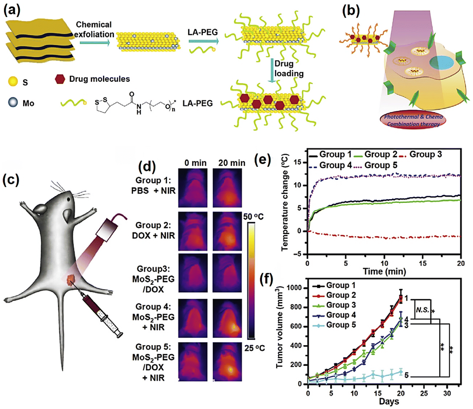 | ||
| Fig. 20 (a) Systematic illustration of the development route of PEG-MoS2 and corresponding drug loading scheme. (b) Depiction of targeted in vitro therapy employing the MoS2/PEG/FA/DOX complex, (c) demonstration for a group of therapy centered on intratumorally introduced complex of MoS2-PEG/DOX, (d) display of 4T1 tumor-bearing mice via IR thermal photograph using an IR camera, (e) monitoring of IR thermal camera for a change in temperature of tumors aimed at different groups in the course of laser treatment as directed in (c), and (f) curves representing the tumor volume progress in different groups of mice when subjected to several treatments. Adapted with permission from ref. 398 Copyright 2014, John Wiley & Sons. | ||
 | ||
| Fig. 21 Depiction of CLEAR device towards optogenetic applications as well as neural imaging: (a) implementation of optogenetics in an animal module. Adapted with permission from ref. 402 Copyright 2013, Proceedings of the National Academy of Sciences. (b) Development route for CLEAR device, (c) presentation of experimental arrangement, (d) blue light stimulus image using an optical fiber, (e) CLEAR device towards the recording of optical evoked potentials (scale bars: x-scale = 50 ms and y-scale = 100 μV), (f) demonstration of full intensity projection of OCT angiogram, and (g) doppler blood flow velocity image. Adapted with permission from ref. 401 Copyright 2014, Nature Publishing Group. | ||
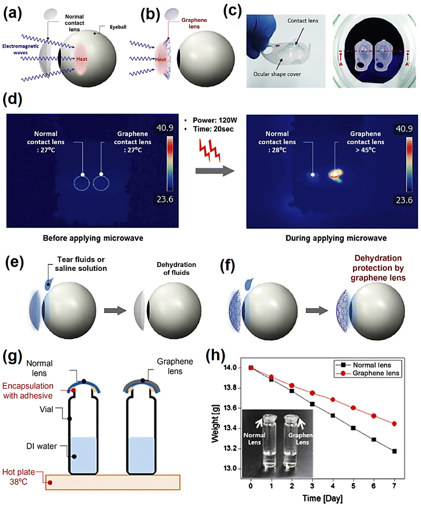 | ||
| Fig. 22 Schematic of the working principle of contact lens coated with graphene: (a) interaction of EM wave and contact lens, which shows that the eye absorbs the EM wave (this may result in heat destruction inside), (b) absorption of EM energy through graphene in addition to heat dissipation before approaching the internal structure of the eye, (c) synthesis of sample aimed at microwave oven testing, (d) measurement of elevated temperature (for the interior of a microwave oven) for graphene-coated lens via displayed photograph using IR camera, (e and f) demonstration of gas-impermeability of graphene, which leads to a reduction in the dehydration of a contact lens, (g) trend of evaporation rate (for water) using the experimental arrangement shown, and (h) measurement of weight loss as a function of time on hot plate (38 °C). Adapted with permission from ref. 403 Copyright 2017, the American Chemical Society. | ||
Electrons in graphene produce oscillations when exposed to electromagnetic radiation, which absorb and discard the electromagnetic energy as heat energy. According to Fig. 22d, when a strong EM with a power of 120 W was illuminated on a graphene-coated contact lens (for 20 s), the temperature of the coated contact lens changed from room temperature (27 °C) to above 45 °C, and the temperature of the uncoated contact lens remained relatively constant.403Fig. 22e and f schematically illustrate that the application of lenses without the graphene coating causes the dehydration of eyeballs, which can result in xerophthalmia (Fig. 22e). In contrast, graphene lenses protect against dehydration (Fig. 22f). The dehydration protection of the graphene-coated contact lenses was validated by mounting the conventional and graphene lenses on water-filled vials. Subsequently, the vials were set on a heated plate at 38 °C (Fig. 22g). One week later, the weight of the vial with the graphene-coated lens decreased by 0.5535 g, while that with the conventional lens decreased by 0.8268 g. This indicates the suitability of graphene to be used as protective material against dehydration (Fig. 22h). Thus, graphene-coated lenses can screen electromagnetic interference and prevent dryness in the eyes. Also, they can be used as a bionic platform in smart technologies for biomedical and healthcare applications in the future.406,407
4 Challenges and prospects
4.1 Pertinent features and common limiting factors
2D materials offer a significant advantage for sensing applications due to their various characteristics. In addition to their outstanding physical and chemical characteristics, 2D materials have a high surface area-to-volume ratio, which is crucial for sensing applications. As a result of such surface- and volume-free nature, high-performance sensing devices can be designed with maximum sensitivity by introducing various alterations 2D materials framework. Different 2D nanostructures undergo oxidation under ambient conditions, leading to structural changes and resulting in the decomposition of the material in some severe cases. Consequently, their application in functional devices is considerably limited. Thus, far out approaches are required to achieve substantial oxidative stability during the synthesis, storage, and practical applications of 2D materials. This can be realized by designing new 2D materials with improved oxidative and thermal stability. Correspondingly, the chemical tunability of 2D materials facilitates the fabrication of multi-component assemblies, which can enable multiplex or multi-analyte detection in a single device. In particular, the presence of free radicals (so-called dangling bonds) and better reactivity of 2D materials can elevate the sensing profile. Also, the non-selective binding of analytes ultimately results in poor selectivity, long response, or even incomplete recovery time. In this case, optical sensors (based on the variations in the PL characteristics of 2D materials following the antigen-analyte interactions with analytes) have been used successfully and extensively utilized for biological and metal-relevant molecules. Not least of all, Electrochemical sensors seem encouraging due to their feasible operations and rapid detection.4.2 Role of defects
Pristine and/or defect-free sheets may not produce strong interactions with target analytes. Furthermore, defects play a critical role in 2D materials, where they enable bandgap engineering and offer modulation of optoelectronic/electronic characteristics. Moreover, defects increase the chemical reactivity of 2D materials, allowing the further chemical functionalization of their reactive sites, which results in higher sensitivity and a small LOD for target analytes. Conversely, the lack of control during defect engineering can produce enduring effects in 2D materials. The most important task to be initiated in the near future is the well-ordered incorporation of ad hoc defects in 2D materials with precise concentration and spatial resolution. Ideally, defect placement should be accompanied by chemical functionalization of reactive sites with a choice of analyte receptors. This can be achieved through a thorough understanding of the principles of molecular recognition. For example, this can be realized by modifying the supramolecular interactions that correspond to ultrasensitive 2D materials and improving the response time of sensors with higher selectivity, thus providing a clear path to industrial production.4.3 Particular aspects of electrochemical sensing
Furthermore, it is essential to link the multi-dimensional aspects of 2D materials to electronic devices, i.e., synergistically integrating multi-functionality. For example, the fabrication of porous conductive materials allows a synergistic connection with the surface, increased hydrophobicity, low resistance to charge transfer, and increased capacitance. These elements can enhance the operation of potentiometric devices. Conversely, during antigen-analyte interactions, the coupling of magnetic exchange and electronic interactions in 2D materials can increase the charge transport perturbations. The evolution of these sensing technologies can lead to extraordinary advances in analytic modes, which include cost, simplicity, and superior sensing profile. The study of new 2D materials is still in its initial stages, and due to the exceptional diversity of these materials, it is possible to further consolidate their place in the field of electrical transduction sensors and nanoscience. Recently, the immense progress and development of 2D materials, including the graphene-based material family, MXene family, and TMDCs, are widely used in numerous devices, including strain and pressure sensors, flexible temperature sensors, and gas sensors (see Tables 1 and 2). Furthermore, industrial and commercial technologies may introduce these materials in the coming years. Generally, flexible electronics (Opto) with superior advances are considered attractive candidates for studying human physiological information, especially in wearable configurations for medical diagnosis and personalized health care. Similarly, some integrated electronics that can detect multiple signals to obtain detailed physiological information have also been examined.4.4 Particular aspects of wearable systems
Graphene and other 2D materials offer outstanding electrical and mechanical properties (e.g., flexibility and stiffness). Material-based 2D sensors can be supported on flexible sheets to fabricate smart wearable devices to monitor the environment/human interface. Furthermore, by integrating 2D materials with electrodes, van der Waals heterostructures from combining different 2D materials can improve the electrical contacts, material stability, and device performance. The fabrication of these heterostructure interfaces in sensing devices has the potential to improve the sensitivity, selectivity, and stability of sensors. Furthermore, developing multifunctional devices, physically and chemically integrated systems, will be a promising route toward accurately assessing physical conditions. Nevertheless, the simultaneous detection of chemical signals and large strain changes is a significant task due to their severe signal crosstalk. In addition, wearable chemical systems with a lower LOD, higher sensitivity, and exceptional selectivity for complex environments of the human body need to be addressed. Furthermore, combining two features, such as diagnosis and therapy, is an alternative operation path to extend their function and applications. Drug delivery and physical therapy (i.e., electrical stimulation and hyperthermia) will be a favorable development as a medical treatment device. Although various research works verify the recovery of human physiological signals, the transition from fundamental research (from laboratories) to industrial products takes a long time. Signal processing with a flexible circuit board, low power consumption, and delicate and modest size should be approved through pragmatic cooperation with electronic engineers. Existing circuit technologies have been assembled using standard chips, which are unsuitable for some particular applications, for example, the chip introduced in a contact lens for intraocular pressure monitoring. In addition, small-scale loop devices with long standby life and working hours are crucial for the round-the-clock observation of human physiological information. To ensure the safety of wearable systems, medical professionals should evaluate the various signals detected by these devices. Additional valuable data can be identified by comparing the results to typical medical test results. Evaluations and long-term observation of human physiological signals will support data consistency, which is significant for impending personal health care. Furthermore, despite the substantial advances in assessing mechanical characteristics based on nanoindentation, the effect of unavoidable factors, such as sample damage during the laborious preparation and testing procedure are insignificant. Future research into 2D ultrathin nanomaterials still requires the development of new 2D materials, large-scale production of high-quality 2D crystals, and use of more accurate computational and experimental models for characterization and measurement. Recent evidence suggest 2D materials can work with “on-the-skin” applications paving the way for their application to detect clinically significant biomarkers. Consequently, these 2D material-based tattoos can be used as dry sensors on the skin with minimal sensitivity to motion artifacts, a significant shortcoming of conventional dry sensors and electrodes for point-of-care health monitoring.4.5 Computational approaches for state-of-the-art sensor design
Computational evaluation coupled with curiosity-driven research can lead to numerous possibilities for the innovation in stimulus-sensitive 2D materials with significant functions in chemical sensing. The creation of computational models and their application in materials design and synthesis are the challenging long-term goals in this field. Consequently, we may see two critical methodologies in the future. Firstly, the open-loop design technique. The growth chamber design and synthesis settings are established by a series of simulations that reflect the experiment thermophysical circumstances, expected growth, and reaction kinetics. This method requires high model fidelity, and a thorough sensitivity analysis must be performed to produce a robust design. Secondly, the closed-loop design, where the models identify system states that are communicated to a controller that continuously changes the growing conditions in real-time. The effectiveness of the design in this technique critically depends on the computational capacity of the models. Future development of multianalyte detection can also be possible through chemical programmability by creating 2D material-based multi-component assemblies. However, current mathematical and numerical models are computationally expensive and often do not simultaneously capture all the physics involved in a 2D material growth process, thus limiting their general application in the active control of 2D material growth. The use of machine learning models trained using experimental and computational databases of 2D material structure and growth conditions, such as that accessible in the 2D Crystal Consortium-Materials Innovation Platform, is a promising technique to overcome this problem. Finally, the models and methods used to understand the growth of 2D materials can be modified to understand the evolution of other materials using the same synthesis methods, such as thin-film CVD growth.4.6 In situ and operando spectroscopic techniques for mechanism understanding
In situ and operando spectroscopic techniques are considered state-of-the-art tools for learning the operating principles and processes involved in gas sensing. A combination of ionsorption, oxygen vacancy, and charge transfer models can provide insight into the sensing mechanisms of chemiresistive gases. Understanding the precise sensing processes of these types of sensor devices using spectroscopic methods in various modes of operation can aid in constructing high-performance intelligent sensor devices. Moreover, extensive theoretical studies are needed to validate the experimental results of operando spectroscopic studies. The benefits of different operando spectroscopic studies and theoretical analyses are thought to provide more information on sensing devices and aid in designing high-performance gas sensors. The use of luminous 2D materials has great potential in biological sensing and imaging applications. The large surface area of 2D materials can function as a platform for multiplex sensing, another potential untapped application. Furthermore, although sensors are performing well in research and development, a satisfactory result for sensor devices has not been achieved thus far. Future research should focus on solving some of these problems and creating reliable, cheap, and environmentally friendly chemical sensors with extremely high selectivity and sensitivity. Another expansion path is sensor technology with portable capabilities.4.7 Concluding remarks, critical comments, and industrial aspects
Convincingly, 2D materials have significant properties in terms of sensing. However, multidisciplinary efforts and cutting-edge research are required to realize their full potential. Further development in this field can be achieved through innovations in the design of 2D materials. The roadmap for developing and discovering 2D materials is progressing rapidly; however, some 2D materials still have to be fully revealed as candidates for chemical sensing. New sensing platforms are revealed every year, and the industry is developing rapidly. Multiplatform sensing using a combination of different materials is the next frontier. Crosslinked heterostructures, which produce distinctive properties that their single 2D equivalents cannot achieve, can be formed not only for 2D-2D blocks but also with other low-dimensional materials. Compared to conventional materials, 2D materials have emerged as the most promising materials for technological applications due to their unique piezoelectric, photoelectric, and mechanical capabilities. In this case, understanding the active sensing physicochemical properties and interactions of the material is crucial to comprehend its sensing mechanisms. The detailed operating principles behind gas sensing devices should be evaluated through rigorous explanation of their physical and synthetic characteristics, including the functionality of sensing materials and their interactions with analyte gas molecules. This can enable the development of optimal high-performance sensor systems. However, there is still a great deal of work to be done on defining the exact sensing mechanisms of these newly discovered materials. Several techniques have been proven to be effective in tuning the gas-sensing properties of 2D materials.In addition, two-dimensional self-powered sensors are considered to have a wide range of applications in biomedicine, environmental sensing, motion tracking, energy harvesting, and smart wearables. Recently, self-powered nanosensors (TENG/PENG) have emerged as a new form of sensors. These devices use nano-effects to ensure continuous operation by harvesting and using energy from the environment. Recent advances in TENG/PENG as a new mechanical energy conversion technology have demonstrated their potential towards self-powered sensors/electronics and micro/nano power sources. They are ideal for portable electronic devices, self-driving micro-nano systems, and the next generation of IoT devices. These sensors offer a variety of benefits, including precision, energy harvesting, biomedical engineering, environmental monitoring, artificial intelligence, and neuromorphic computing. Because graphene has high thermal conductivity and a negative thermal expansion coefficient, studies on its thermal properties are becoming increasingly crucial for graphene-based self-powered sensors. The development of 2D material-based self-powered NG sensors is still in its early stages, and further studies are required to select and optimize 2D materials and design optimization. A growing number of 2D materials are being discovered, resulting in the greater use of 2D self-powered sensors for human monitoring, energy harvesting, biomedicine, and artificial intelligence.
The Internet of Things (IoT) is at the heart of the global information industry. Sensors have become common due to their high integration, simplicity, portability, and ease of commercialization. Together with its advancement, IoT also faces many technological challenges. One example is sensors, which have become the most significant obstacle in the growth of IoT. Although small-scale applications can reduce the power consumption to microwatts, large-scale applications can result in surprising power consumption, resulting in a shorter shelf life and environmental contamination.
Primarily, the study on 2D materials has lasted 19 years since their first report (e.g., graphene). All the literature on this subject leads the way and ousts any doubts about their potential use in sensing applications. However, currently fewer products on the market that contain 2D materials. While challenging, the long-term goal of researchers is commercializing the sensing devices based on 2D materials. However, 2D material deposition and growth at the wafer scale may be appropriate. Nevertheless, contamination and defects still do not fully comply with industry standards for manufacturing. Accordingly, reliable product design, scalability, and low-cost manufacturing are essential features to consider from an industrial perspective and market competition. Due to the manufacturing limitation for effective 2D materials, various complicated procedures have been widely implemented, disrupting their subsequent practical applications. Additionally, large-scale manufacturing techniques are needed for low-cost, scalable systems. By thoroughly analyzing 2D-based sensing devices and the challenges involved, this review paper aimed to provide readers with a better understanding of the fundamental research and academia-industry connections.
Conflicts of interest
The authors declare no conflict of interest.Acknowledgements
The authors are thankful to all individuals and organizations who permitted us to republish their figures and other relevant information.References
- K. S. Novoselov, A. K. Geim, S. V. Morozov, D. Jiang, M. I. Katsnelson, I. V. Grigorieva, S. V. Dubonos and A. A. Firsov, Nature, 2005, 438, 197–200 CrossRef CAS PubMed.
- A. C. Ferrari, F. Bonaccorso, V. Fal'ko, K. S. Novoselov, S. Roche, P. Bøggild, S. Borini, F. H. L. Koppens, V. Palermo, N. Pugno, J. A. Garrido, R. Sordan, A. Bianco, L. Ballerini, M. Prato, E. Lidorikis, J. Kivioja, C. Marinelli, T. Ryhänen, A. Morpurgo, J. N. Coleman, V. Nicolosi, L. Colombo, A. Fert, M. Garcia-Hernandez, A. Bachtold, G. F. Schneider, F. Guinea, C. Dekker, M. Barbone, Z. Sun, C. Galiotis, A. N. Grigorenko, G. Konstantatos, A. Kis, M. Katsnelson, L. Vandersypen, A. Loiseau, V. Morandi, D. Neumaier, E. Treossi, V. Pellegrini, M. Polini, A. Tredicucci, G. M. Williams, B. Hee Hong, J.-H. Ahn, J. Min Kim, H. Zirath, B. J. van Wees, H. van der Zant, L. Occhipinti, A. Di Matteo, I. A. Kinloch, T. Seyller, E. Quesnel, X. Feng, K. Teo, N. Rupesinghe, P. Hakonen, S. R. T. Neil, Q. Tannock, T. Löfwander and J. Kinaret, Nanoscale, 2015, 7, 4598–4810 RSC.
- M. Chakraborty and M. S. J. Hashmi, Adv. Mater. Process. Technol., 2018, 4, 573–602 Search PubMed.
- M. J. Molaei, M. Younas and M. Rezakazemi, ACS Appl. Electron. Mater., 2021, 3, 5165–5187 CrossRef CAS.
- M. W. Barsoum, Prog. Solid State Chem., 2000, 28, 201–281 CrossRef CAS.
- Q. H. Wang, K. Kalantar-Zadeh, A. Kis, J. N. Coleman and M. S. Strano, Nat. Nanotechnol., 2012, 7, 699–712 CrossRef CAS PubMed.
- L. Li, Y. Yu, G. J. Ye, Q. Ge, X. Ou, H. Wu, D. Feng, X. H. Chen and Y. Zhang, Nat. Nanotechnol., 2014, 9, 372–377 CrossRef CAS PubMed.
- H. Liu, A. T. Neal, Z. Zhu, Z. Luo, X. Xu, D. Tománek and P. D. Ye, ACS Nano, 2014, 8, 4033–4041 CrossRef CAS PubMed.
- A. Raza, U. Qumar, A. A. Rafi and M. Ikram, Sustainable Mater. Technol., 2022, 33, e00462 CrossRef CAS.
- A. Gupta, T. Sakthivel and S. Seal, Prog. Mater. Sci., 2015, 73, 44–126 CrossRef CAS.
- A. S. Mayorov, R. V. Gorbachev, S. V. Morozov, L. Britnell, R. Jalil, L. A. Ponomarenko, P. Blake, K. S. Novoselov, K. Watanabe, T. Taniguchi and A. K. Geim, Nano Lett., 2011, 11, 2396–2399 CrossRef CAS PubMed.
- C. Schneider, M. M. Glazov, T. Korn, S. Höfling and B. Urbaszek, Nat. Commun., 2018, 9, 2695 CrossRef PubMed.
- N. Zibouche, P. Philipsen, A. Kuc and T. Heine, Phys. Rev. B: Condens. Matter Mater. Phys., 2014, 90, 125440 CrossRef.
- J. Wang, I. Verzhbitskiy and G. Eda, Adv. Mater., 2018, 30, 1802687 CrossRef PubMed.
- M. Long, P. Wang, H. Fang and W. Hu, Adv. Funct. Mater., 2019, 29, 1803807 CrossRef.
- X. Cao, C. Ding, C. Zhang, W. Gu, Y. Yan, X. Shi and Y. Xian, J. Mater. Chem. B, 2018, 6, 8011–8036 RSC.
- A. Daus, S. Vaziri, V. Chen, Ç. Köroğlu, R. W. Grady, C. S. Bailey, H. R. Lee, K. Schauble, K. Brenner and E. Pop, Nat. Electron., 2021, 4, 495–501 CrossRef CAS.
- A. Shahin, K. Ibrahim, F. Ye, R. Karimi, J. Sanderson and K. P. Musselman, Sens. Actuators, B, 2022, 359, 131576 CrossRef CAS.
- R. Kumar, N. Goel, M. Hojamberdiev and M. Kumar, Sens. Actuators, A, 2020, 303, 111875 CrossRef CAS.
- Y. Hu, Y. Huang, C. Tan, X. Zhang, Q. Lu, M. Sindoro, X. Huang, W. Huang, L. Wang and H. Zhang, Mater. Chem. Front., 2017, 1, 24–36 RSC.
- L.-x. Yu and R.-t. Lv, New Carbon Mater., 2021, 36, 995–1012 CrossRef CAS.
- M. Pumera and A. H. Loo, TrAC, Trends Anal. Chem., 2014, 61, 49–53 CrossRef CAS.
- U. Qumar, J. Z. Hassan, R. A. Bhatti, A. Raza, G. Nazir, W. Nabgan and M. Ikram, J. Mater. Sci. Technol., 2022, 131, 122–166 CrossRef.
- C. Anichini, W. Czepa, D. Pakulski, A. Aliprandi, A. Ciesielski and P. Samorì, Chem. Soc. Rev., 2018, 47, 4860–4908 RSC.
- C. Zhu, Z. Zeng, H. Li, F. Li, C. Fan and H. Zhang, J. Am. Chem. Soc., 2013, 135, 5998–6001 CrossRef CAS PubMed.
- D. Dinda, A. Gupta, B. K. Shaw, S. Sadhu and S. K. Saha, ACS Appl. Mater. Interfaces, 2014, 6, 10722–10728 CrossRef CAS PubMed.
- A. Raza, Y. Zhang, A. Cassinese and G. Li, Catalysts, 2022, 12, 1613 CrossRef CAS.
- J. Z. Hassan, A. Raza, U. Qumar and G. Li, Sustainable Mater. Technol., 2022, 33, e00478 CrossRef CAS.
- F. K. Perkins, A. L. Friedman, E. Cobas, P. M. Campbell, G. G. Jernigan and B. T. Jonker, Nano Lett., 2013, 13, 668–673 CrossRef CAS PubMed.
- C. Yim, K. Lee, N. McEvoy, M. O'Brien, S. Riazimehr, N. C. Berner, C. P. Cullen, J. Kotakoski, J. C. Meyer, M. C. Lemme and G. S. Duesberg, ACS Nano, 2016, 10, 9550–9558 CrossRef CAS PubMed.
- Y. Liu, M. Pharr and G. A. Salvatore, ACS Nano, 2017, 11, 9614–9635 CrossRef CAS PubMed.
- Y. Zang, F. Zhang, C.-a. Di and D. Zhu, Mater. Horiz., 2015, 2, 140–156 RSC.
- S. Xu, Y. Zhang, L. Jia, E. Mathewson Kyle, K.-I. Jang, J. Kim, H. Fu, X. Huang, P. Chava, R. Wang, S. Bhole, L. Wang, J. Na Yoon, Y. Guan, M. Flavin, Z. Han, Y. Huang and A. Rogers John, Science, 2014, 344, 70–74 CrossRef CAS PubMed.
- T. Yamada, Y. Hayamizu, Y. Yamamoto, Y. Yomogida, A. Izadi-Najafabadi, D. N. Futaba and K. Hata, Nat. Nanotechnol., 2011, 6, 296–301 CrossRef CAS PubMed.
- S. Chen, Y. Song, D. Ding, Z. Ling and F. Xu, Adv. Funct. Mater., 2018, 28, 1802547 CrossRef.
- W. Gao, S. Emaminejad, H. Y. Y. Nyein, S. Challa, K. Chen, A. Peck, H. M. Fahad, H. Ota, H. Shiraki, D. Kiriya, D.-H. Lien, G. A. Brooks, R. W. Davis and A. Javey, Nature, 2016, 529, 509–514 CrossRef CAS PubMed.
- A. J. Bandodkar, I. Jeerapan and J. Wang, ACS Sens., 2016, 1, 464–482 CrossRef CAS.
- Z. Meng, R. M. Stolz, L. Mendecki and K. A. Mirica, Chem. Rev., 2019, 119, 478–598 CrossRef CAS PubMed.
- Y. Pang, Z. Yang, Y. Yang and T.-L. Ren, Small, 2020, 16, 1901124 CrossRef CAS PubMed.
- N. Rohaizad, C. C. Mayorga-Martinez, M. Fojtů, N. M. Latiff and M. Pumera, Chem. Soc. Rev., 2021, 50, 619–657 RSC.
- K. Khan, A. K. Tareen, L. Wang, M. Aslam, C. Ma, N. Mahmood, Z. Ouyang, H. Zhang and Z. Guo, Adv. Funct. Mater., 2021, 31, 2005957 CrossRef CAS.
- A. Majed, M. Kothakonda, F. Wang, E. N. Tseng, K. Prenger, X. Zhang, P. O. Å. Persson, J. Wei, J. Sun and M. Naguib, Adv. Mater., 2022, 34, 2200574 CrossRef CAS PubMed.
- Z. Guo, J. Zhou and Z. Sun, J. Mater. Chem. A, 2017, 5, 23530–23535 RSC.
- H. Zhang, H. Xiang, F.-z. Dai, Z. Zhang and Y. Zhou, J. Mater. Sci. Technol., 2018, 34, 2022–2026 CrossRef CAS.
- M. Dahri, A. Miri Jahromi, A. Nikzad, M. Mohammadgholian, M. Rahmanian, S. S. Abolmaali and R. Maleki, J. Biomol. Struct. Dyn., 2021, 1–9, DOI:10.1080/07391102.2021.1969288.
- M. Naguib, M. Kurtoglu, V. Presser, J. Lu, J. Niu, M. Heon, L. Hultman, Y. Gogotsi and M. W. Barsoum, Adv. Mater., 2011, 23, 4248–4253 CrossRef CAS PubMed.
- F. Wang, C. Yang, C. Duan, D. Xiao, Y. Tang and J. Zhu, J. Electrochem. Soc., 2014, 162, B16–B21 CrossRef.
- H. Lin, X. Wang, L. Yu, Y. Chen and J. Shi, Nano Lett., 2017, 17, 384–391 CrossRef CAS PubMed.
- K. S. Novoselov, A. K. Geim, S. V. Morozov, D. Jiang, Y. Zhang, S. V. Dubonos, I. V. Grigorieva and A. A. Firsov, Science, 2004, 306, 666–669 CrossRef CAS PubMed.
- N. Mohanty and V. Berry, Nano Lett., 2008, 8, 4469–4476 CrossRef CAS PubMed.
- Z. Liu, J. T. Robinson, X. Sun and H. Dai, J. Am. Chem. Soc., 2008, 130, 10876–10877 CrossRef CAS PubMed.
- Y. Hernandez, V. Nicolosi, M. Lotya, F. M. Blighe, Z. Sun, S. De, I. T. McGovern, B. Holland, M. Byrne, Y. K. Gun'Ko, J. J. Boland, P. Niraj, G. Duesberg, S. Krishnamurthy, R. Goodhue, J. Hutchison, V. Scardaci, A. C. Ferrari and J. N. Coleman, Nat. Nanotechnol., 2008, 3, 563–568 CrossRef CAS PubMed.
- P. Joensen, R. F. Frindt and S. R. Morrison, Mater. Res. Bull., 1986, 21, 457–461 CrossRef CAS.
- J. N. Coleman, M. Lotya, A. O'Neill, S. D. Bergin, P. J. King, U. Khan, K. Young, A. Gaucher, S. De, R. J. Smith, I. V. Shvets, S. K. Arora, G. Stanton, H.-Y. Kim, K. Lee, G. T. Kim, G. S. Duesberg, T. Hallam, J. J. Boland, J. J. Wang, J. F. Donegan, J. C. Grunlan, G. Moriarty, A. Shmeliov, R. J. Nicholls, J. M. Perkins, E. M. Grieveson, K. Theuwissen, D. W. McComb, P. D. Nellist and V. Nicolosi, Science, 2011, 331, 568–571 CrossRef CAS PubMed.
- H. Li, Z. Yin, Q. He, H. Li, X. Huang, G. Lu, D. W. H. Fam, A. I. Y. Tok, Q. Zhang and H. Zhang, Small, 2012, 8, 63–67 CrossRef CAS PubMed.
- S. S. Chou, B. Kaehr, J. Kim, B. M. Foley, M. De, P. E. Hopkins, J. Huang, C. J. Brinker and V. P. Dravid, Angew. Chem., Int. Ed., 2013, 52, 4160–4164 CrossRef CAS PubMed.
- J. Li, X.-Y. Wang, X.-R. Liu, Z. Jin, D. Wang and L.-J. Wan, J. Mater. Chem. C, 2015, 3, 3530–3535 RSC.
- I. V. Vlassiouk, Y. Stehle, P. R. Pudasaini, R. R. Unocic, P. D. Rack, A. P. Baddorf, I. N. Ivanov, N. V. Lavrik, F. List, N. Gupta, K. V. Bets, B. I. Yakobson and S. N. Smirnov, Nat. Mater., 2018, 17, 318–322 CrossRef CAS PubMed.
- A. H. Castro Neto, F. Guinea, N. M. R. Peres, K. S. Novoselov and A. K. Geim, Rev. Mod. Phys., 2009, 81, 109–162 CrossRef CAS.
- Q. He, S. Wu, Z. Yin and H. Zhang, Chem. Sci., 2012, 3, 1764–1772 RSC.
- L. H. Li and Y. Chen, Adv. Funct. Mater., 2016, 26, 2594–2608 CrossRef CAS.
- M. Chhowalla, H. S. Shin, G. Eda, L.-J. Li, K. P. Loh and H. Zhang, Nat. Chem., 2013, 5, 263–275 CrossRef PubMed.
- K. Kalantar-zadeh, J. Z. Ou, T. Daeneke, A. Mitchell, T. Sasaki and M. S. Fuhrer, Appl. Mater. Today, 2016, 5, 73–89 CrossRef.
- L. Sun, M. G. Campbell and M. Dincă, Angew. Chem., Int. Ed., 2016, 55, 3566–3579 CrossRef CAS PubMed.
- E. Jin, M. Asada, Q. Xu, S. Dalapati, A. Addicoat Matthew, A. Brady Michael, H. Xu, T. Nakamura, T. Heine, Q. Chen and D. Jiang, Science, 2017, 357, 673–676 CrossRef CAS PubMed.
- C. Tan, X. Cao, X.-J. Wu, Q. He, J. Yang, X. Zhang, J. Chen, W. Zhao, S. Han, G.-H. Nam, M. Sindoro and H. Zhang, Chem. Rev., 2017, 117, 6225–6331 CrossRef CAS PubMed.
- F. Bonaccorso, L. Colombo, G. Yu, M. Stoller, V. Tozzini, A. C. Ferrari, R. S. Ruoff and V. Pellegrini, Science, 2015, 347, 1246501 CrossRef PubMed.
- J. H. Gosling, O. Makarovsky, F. Wang, N. D. Cottam, M. T. Greenaway, A. Patanè, R. D. Wildman, C. J. Tuck, L. Turyanska and T. M. Fromhold, Commun. Phys., 2021, 4, 30 CrossRef CAS.
- Y. Zhang, J. P. Small, W. V. Pontius and P. Kim, Appl. Phys. Lett., 2005, 86, 073104 CrossRef.
- A. Chaves, J. G. Azadani, H. Alsalman, D. R. da Costa, R. Frisenda, A. J. Chaves, S. H. Song, Y. D. Kim, D. He, J. Zhou, A. Castellanos-Gomez, F. M. Peeters, Z. Liu, C. L. Hinkle, S.-H. Oh, P. D. Ye, S. J. Koester, Y. H. Lee, P. Avouris, X. Wang and T. Low, npj 2D Mater. Appl., 2020, 4, 29 CrossRef CAS.
- S. Manzeli, D. Ovchinnikov, D. Pasquier, O. V. Yazyev and A. Kis, Nat. Rev. Mater., 2017, 2, 17033 CrossRef CAS.
- K. F. Mak, C. Lee, J. Hone, J. Shan and T. F. Heinz, Phys. Rev. Lett., 2010, 105, 136805 CrossRef PubMed.
- S. Barua, H. S. Dutta, S. Gogoi, R. Devi and R. Khan, ACS Appl. Nano Mater., 2018, 1, 2–25 CrossRef CAS.
- D. Le, T. B. Rawal and T. S. Rahman, J. Phys. Chem. C, 2014, 118, 5346–5351 CrossRef CAS.
- S. Ali, A. Raza, A. M. Afzal, M. W. Iqbal, M. Hussain, M. Imran and M. A. Assiri, Adv. Mater. Interfaces, 2022, 9, 2200556 CrossRef CAS.
- A. Bolotsky, D. Butler, C. Dong, K. Gerace, N. R. Glavin, C. Muratore, J. A. Robinson and A. Ebrahimi, ACS Nano, 2019, 13, 9781–9810 CrossRef CAS PubMed.
- Y. Wang, Y. Shao, D. W. Matson, J. Li and Y. Lin, ACS Nano, 2010, 4, 1790–1798 CrossRef CAS PubMed.
- K. Kalantar-zadeh and J. Z. Ou, ACS Sens., 2016, 1, 5–16 CrossRef CAS.
- Z. Li and S. L. Wong, Mater. Sci. Eng., C, 2017, 70, 1095–1106 CrossRef CAS PubMed.
- A. Hirsch and F. Hauke, Angew. Chem., Int. Ed., 2018, 57, 4338–4354 CrossRef CAS PubMed.
- V. Georgakilas, J. N. Tiwari, K. C. Kemp, J. A. Perman, A. B. Bourlinos, K. S. Kim and R. Zboril, Chem. Rev., 2016, 116, 5464–5519 CrossRef CAS PubMed.
- G. Reina, J. M. González-Domínguez, A. Criado, E. Vázquez, A. Bianco and M. Prato, Chem. Soc. Rev., 2017, 46, 4400–4416 RSC.
- J. Wan, S. D. Lacey, J. Dai, W. Bao, M. S. Fuhrer and L. Hu, Chem. Soc. Rev., 2016, 45, 6742–6765 RSC.
- Y. Xu, X. Xie, R. Zhang and W. Yuan, Sens. Actuators, B, 2022, 372, 132670 CrossRef CAS.
- S. Eissa, G. C. Jimenez, F. Mahvash, A. Guermoune, C. Tlili, T. Szkopek, M. Zourob and M. Siaj, Nano Res., 2015, 8, 1698–1709 CrossRef CAS.
- F. Khurshid, M. Jeyavelan, K. Takahashi, M. S. Leo Hudson and S. Nagarajan, RSC Adv., 2018, 8, 20440–20449 RSC.
- M. V. Sulleiro, A. Dominguez-Alfaro, N. Alegret, A. Silvestri and I. J. Gómez, Sens. Bio-Sens. Res., 2022, 38, 100540 CrossRef.
- M. Zeng, Y. Xiao, J. Liu, K. Yang and L. Fu, Chem. Rev., 2018, 118, 6236–6296 CrossRef CAS PubMed.
- F. Schedin, A. K. Geim, S. V. Morozov, E. W. Hill, P. Blake, M. I. Katsnelson and K. S. Novoselov, Nat. Mater., 2007, 6, 652–655 CrossRef CAS PubMed.
- A. Nag, A. Mitra and S. C. Mukhopadhyay, Sens. Actuators, A, 2018, 270, 177–194 CrossRef CAS.
- J. Martincová, M. Otyepka and P. Lazar, Chem.–Eur. J., 2017, 23, 13233–13239 CrossRef PubMed.
- J. Gao, B. Li, J. Tan, P. Chow, T.-M. Lu and N. Koratkar, ACS Nano, 2016, 10, 2628–2635 CrossRef CAS PubMed.
- J.-W. Jiang, Front. Phys., 2015, 10, 287–302 CrossRef.
- J. Yoon, J. Lim, M. Shin, S.-N. Lee and J.-W. Choi, Materials, 2021, 14, 518 CrossRef CAS PubMed.
- Z. U. D. Babar, B. Della Ventura, R. Velotta and V. Iannotti, RSC Adv., 2022, 12, 19590–19610 RSC.
- K. Khan, J. Li, W. Zou, W. Xu, Y. Yang and W. Song, J. Wuhan Univ. Technol., Mater. Sci. Ed., 2016, 31, 1201–1205 CrossRef CAS.
- K. Khan, A. K. Tareen, M. Aslam, Y. Zhang, R. Wang, Z. Ouyang, Z. Gou and H. Zhang, Nanoscale, 2019, 11, 21622–21678 RSC.
- A. J. Mannix, X.-F. Zhou, B. Kiraly, J. D. Wood, D. Alducin, B. D. Myers, X. Liu, B. L. Fisher, U. Santiago, J. R. Guest, M. J. Yacaman, A. Ponce, A. R. Oganov, M. C. Hersam and N. P. Guisinger, Science, 2015, 350, 1513–1516 CrossRef CAS PubMed.
- B. Feng, J. Zhang, R.-Y. Liu, T. Iimori, C. Lian, H. Li, L. Chen, K. Wu, S. Meng, F. Komori and I. Matsuda, Phys. Rev. B, 2016, 94, 041408 CrossRef.
- Y. Wang, J. Fan and M. Trenary, Chem. Mater., 1993, 5, 192–198 CrossRef CAS.
- F. Xia, H. Wang, D. Xiao, M. Dubey and A. Ramasubramaniam, Nat. Photonics, 2014, 8, 899–907 CrossRef CAS.
- C. R. Dean, A. F. Young, I. Meric, C. Lee, L. Wang, S. Sorgenfrei, K. Watanabe, T. Taniguchi, P. Kim, K. L. Shepard and J. Hone, Nat. Nanotechnol., 2010, 5, 722–726 CrossRef CAS PubMed.
- X. Huang, P. Sheng, Z. Tu, F. Zhang, J. Wang, H. Geng, Y. Zou, C.-a. Di, Y. Yi, Y. Sun, W. Xu and D. Zhu, Nat. Commun., 2015, 6, 7408 CrossRef CAS PubMed.
- W. Bao, X. Cai, D. Kim, K. Sridhara and M. S. Fuhrer, Appl. Phys. Lett., 2013, 102, 042104 CrossRef.
- D. J. Perello, S. H. Chae, S. Song and Y. H. Lee, Nat. Commun., 2015, 6, 7809 CrossRef CAS PubMed.
- Y. Wang, Y. Chen, S. D. Lacey, L. Xu, H. Xie, T. Li, V. A. Danner and L. Hu, Mater. Today, 2018, 21, 186–192 CrossRef CAS.
- X. Yang, C. Shang, S. Zhou and J. Zhao, Nanoscale Horiz., 2020, 5, 1106–1115 RSC.
- C. Zhang, B. Anasori, A. Seral-Ascaso, S.-H. Park, N. McEvoy, A. Shmeliov, G. S. Duesberg, J. N. Coleman, Y. Gogotsi and V. Nicolosi, Adv. Mater., 2017, 29, 1702678 CrossRef PubMed.
- K. Hantanasirisakul, M.-Q. Zhao, P. Urbankowski, J. Halim, B. Anasori, S. Kota, C. E. Ren, M. W. Barsoum and Y. Gogotsi, Adv. Electron. Mater., 2016, 2, 1600050 CrossRef.
- X. Jiang, A. V. Kuklin, A. Baev, Y. Ge, H. Ågren, H. Zhang and P. N. Prasad, Phys. Rep., 2020, 848, 1–58 CrossRef CAS.
- I. R. Shein and A. L. Ivanovskii, Comput. Mater. Sci., 2012, 65, 104–114 CrossRef CAS.
- C. J. Zhang, S. Pinilla, N. McEvoy, C. P. Cullen, B. Anasori, E. Long, S.-H. Park, A. Seral-Ascaso, A. Shmeliov, D. Krishnan, C. Morant, X. Liu, G. S. Duesberg, Y. Gogotsi and V. Nicolosi, Chem. Mater., 2017, 29, 4848–4856 CrossRef CAS.
- M. Mozafari and M. Soroush, Mater. Adv., 2021, 2, 7277–7307 RSC.
- S. Kumar, Y. Lei, N. H. Alshareef, M. A. Quevedo-Lopez and K. N. Salama, Biosens. Bioelectron., 2018, 121, 243–249 CrossRef CAS PubMed.
- W. Y. Chen, S.-N. Lai, C.-C. Yen, X. Jiang, D. Peroulis and L. A. Stanciu, ACS Nano, 2020, 14, 11490–11501 CrossRef CAS PubMed.
- J. Huang, Z. Li, Y. Mao and Z. Li, Nano Sel., 2021, 2, 1480–1508 CrossRef CAS.
- H. Lin, Y. Chen and J. Shi, Adv. Sci., 2018, 5, 1800518 CrossRef PubMed.
- Y. Pei, X. Zhang, Z. Hui, J. Zhou, X. Huang, G. Sun and W. Huang, ACS Nano, 2021, 15, 3996–4017 CrossRef CAS PubMed.
- L. Chen, X. Dai, W. Feng and Y. Chen, Acc. Mater. Res., 2022, 3, 785–798 CrossRef CAS.
- J. Wang, F. Ma, W. Liang and M. Sun, Mater. Today Phys., 2017, 2, 6–34 CrossRef.
- X. Huang, Z. Yin, S. Wu, X. Qi, Q. He, Q. Zhang, Q. Yan, F. Boey and H. Zhang, Small, 2011, 7, 1876–1902 CrossRef CAS PubMed.
- Y. Zhang, T.-T. Tang, C. Girit, Z. Hao, M. C. Martin, A. Zettl, M. F. Crommie, Y. R. Shen and F. Wang, Nature, 2009, 459, 820–823 CrossRef CAS PubMed.
- C.-N. Yeh, K. Raidongia, J. Shao, Q.-H. Yang and J. Huang, Nat. Chem., 2015, 7, 166–170 CrossRef CAS PubMed.
- T. Kuila, S. Bose, P. Khanra, A. K. Mishra, N. H. Kim and J. H. Lee, Biosens. Bioelectron., 2011, 26, 4637–4648 CrossRef CAS PubMed.
- V. Georgakilas, M. Otyepka, A. B. Bourlinos, V. Chandra, N. Kim, K. C. Kemp, P. Hobza, R. Zboril and K. S. Kim, Chem. Rev., 2012, 112, 6156–6214 CrossRef CAS PubMed.
- R. Zhou and H. Gao, WIREs Nanomedicine and Nanobiotechnology, 2014, 6, 452–474 CrossRef CAS PubMed.
- S. Syama and P. V. Mohanan, Int. J. Biol. Macromol., 2016, 86, 546–555 CrossRef CAS PubMed.
- S. Pattnaik, K. Swain and Z. Lin, J. Mater. Chem. B, 2016, 4, 7813–7831 RSC.
- B. Radisavljevic, A. Radenovic, J. Brivio, V. Giacometti and A. Kis, Nat. Nanotechnol., 2011, 6, 147–150 CrossRef CAS PubMed.
- G. H. Jeong, S. P. Sasikala, T. Yun, G. Y. Lee, W. J. Lee and S. O. Kim, Adv. Mater., 2020, 32, 1907006 CrossRef CAS PubMed.
- L. Nurdiwijayanto, R. Ma, N. Sakai and T. Sasaki, Inorg. Chem., 2017, 56, 7620–7623 CrossRef CAS PubMed.
- D.-W. Lee, J. Lee, I. Y. Sohn, B.-Y. Kim, Y. M. Son, H. Bark, J. Jung, M. Choi, T. H. Kim, C. Lee and N.-E. Lee, Nano Res., 2015, 8, 2340–2350 CrossRef CAS.
- J. H. Appel, D. O. Li, J. D. Podlevsky, A. Debnath, A. A. Green, Q. H. Wang and J. Chae, ACS Biomater. Sci. Eng., 2016, 2, 361–367 CrossRef CAS PubMed.
- H. Hu, A. Zavabeti, H. Quan, W. Zhu, H. Wei, D. Chen and J. Z. Ou, Biosens. Bioelectron., 2019, 142, 111573 CrossRef CAS PubMed.
- L. Wang, D. Xu, L. Jiang, J. Gao, Z. Tang, Y. Xu, X. Chen and H. Zhang, Adv. Funct. Mater., 2021, 31, 2004408 CrossRef CAS.
- Y. Xiao, Y. Li, Z. Guo, C. Tang, B. Sa, N. Miao, J. Zhou and Z. Sun, Appl. Surf. Sci., 2021, 566, 150634 CrossRef CAS.
- G. Yildiz, M. Bolton-Warberg and F. Awaja, Acta Biomater., 2021, 131, 62–79 CrossRef CAS PubMed.
- L. J. Hubble, J. S. Cooper, A. Sosa-Pintos, H. Kiiveri, E. Chow, M. S. Webster, L. Wieczorek and B. Raguse, ACS Comb. Sci., 2015, 17, 120–129 CrossRef CAS PubMed.
- B. Raguse, E. Chow, C. S. Barton and L. Wieczorek, Anal. Chem., 2007, 79, 7333–7339 CrossRef CAS PubMed.
- C. E. Davis, C. K. Ho, R. C. Hughes and M. L. Thomas, Sens. Actuators, B, 2005, 104, 207–216 CrossRef CAS.
- Y. Liu, J. Parisi, X. Sun and Y. Lei, J. Mater. Chem. A, 2014, 2, 9919–9943 RSC.
- S. Ammu, V. Dua, S. R. Agnihotra, S. P. Surwade, A. Phulgirkar, S. Patel and S. K. Manohar, J. Am. Chem. Soc., 2012, 134, 4553–4556 CrossRef CAS PubMed.
- J. D. Fowler, M. J. Allen, V. C. Tung, Y. Yang, R. B. Kaner and B. H. Weiller, ACS Nano, 2009, 3, 301–306 CrossRef CAS PubMed.
- B. Cho, M. G. Hahm, M. Choi, J. Yoon, A. R. Kim, Y.-J. Lee, S.-G. Park, J.-D. Kwon, C. S. Kim, M. Song, Y. Jeong, K.-S. Nam, S. Lee, T. J. Yoo, C. G. Kang, B. H. Lee, H. C. Ko, P. M. Ajayan and D.-H. Kim, Sci. Rep., 2015, 5, 8052 CrossRef CAS PubMed.
- H. Wohltjen, Sens. Actuators, 1984, 5, 307–325 CrossRef CAS.
- R. Arsat, M. Breedon, M. Shafiei, P. G. Spizziri, S. Gilje, R. B. Kaner, K. Kalantar-zadeh and W. Wlodarski, Chem. Phys. Lett., 2009, 467, 344–347 CrossRef CAS.
- A. J. Ricco, S. J. Martin and T. E. Zipperian, Sens. Actuators, 1985, 8, 319–333 CrossRef CAS.
- W. P. Jakubik, M. W. Urbańczyk, S. Kochowski and J. Bodzenta, Sens. Actuators, B, 2002, 82, 265–271 CrossRef CAS.
- W. Yang, L. Gan, H. Li and T. Zhai, Inorg. Chem. Front., 2016, 3, 433–451 RSC.
- B. Kumar, K. Min, M. Bashirzadeh, A. B. Farimani, M. H. Bae, D. Estrada, Y. D. Kim, P. Yasaei, Y. D. Park, E. Pop, N. R. Aluru and A. Salehi-Khojin, Nano Lett., 2013, 13, 1962–1968 CrossRef CAS PubMed.
- W. Xuan, M. He, N. Meng, X. He, W. Wang, J. Chen, T. Shi, T. Hasan, Z. Xu, Y. Xu and J. K. Luo, Sci. Rep., 2014, 4, 7206 CrossRef CAS PubMed.
- G. Korotcenkov and B. K. Cho, Sens. Actuators, B, 2013, 188, 709–728 CrossRef CAS.
- G. Di Francia, B. Alfano and V. La Ferrara, J. Sens., 2009, 2009, 659275 Search PubMed.
- L. Zhang, K. Khan, J. Zou, H. Zhang and Y. Li, Adv. Mater. Interfaces, 2019, 6, 1901329 CrossRef.
- G. Korotcenkov, Mater. Sci. Eng., B, 2007, 139, 1–23 CrossRef CAS.
- C. Wang, L. Yin, L. Zhang, D. Xiang and R. Gao, Sensors, 2010, 10, 2088–2106 CrossRef CAS PubMed.
- H. Yang, J. Heo, S. Park, J. Song Hyun, H. Seo David, K.-E. Byun, P. Kim, I. Yoo, H.-J. Chung and K. Kim, Science, 2012, 336, 1140–1143 CrossRef CAS PubMed.
- A. Singh, M. A. Uddin, T. Sudarshan and G. Koley, Small, 2014, 10, 1555–1565 CrossRef CAS PubMed.
- B. P. Luther, S. D. Wolter and S. E. Mohney, Sens. Actuators, B, 1999, 56, 164–168 CrossRef CAS.
- B. Liu, L. Chen, G. Liu, A. N. Abbas, M. Fathi and C. Zhou, ACS Nano, 2014, 8, 5304–5314 CrossRef CAS PubMed.
- Y. Kim, S.-K. Kang, N.-C. Oh, H.-D. Lee, S.-M. Lee, J. Park and H. Kim, ACS Appl. Mater. Interfaces, 2019, 11, 38902–38909 CrossRef CAS PubMed.
- T. Pham, G. Li, E. Bekyarova, M. E. Itkis and A. Mulchandani, ACS Nano, 2019, 13, 3196–3205 CrossRef CAS PubMed.
- A. Liu, S. Lv, L. Jiang, F. Liu, L. Zhao, J. Wang, X. Hu, Z. Yang, J. He, C. Wang, X. Yan, P. Sun, K. Shimanoe and G. Lu, Sens. Actuators, B, 2021, 332, 129444 CrossRef CAS.
- P. Bharathi, S. Harish, M. Shimomura, S. Ponnusamy, M. Krishna Mohan, J. Archana and M. Navaneethan, Sens. Actuators, B, 2022, 360, 131600 CrossRef CAS.
- Q. He, Z. Zeng, Z. Yin, H. Li, S. Wu, X. Huang and H. Zhang, Small, 2012, 8, 2994–2999 CrossRef CAS PubMed.
- D. J. Late, Y.-K. Huang, B. Liu, J. Acharya, S. N. Shirodkar, J. Luo, A. Yan, D. Charles, U. V. Waghmare, V. P. Dravid and C. N. R. Rao, ACS Nano, 2013, 7, 4879–4891 CrossRef CAS PubMed.
- Y. Niu, J. Zeng, X. Liu, J. Li, Q. Wang, H. Li, N. F. d. Rooij, Y. Wang and G. Zhou, Adv. Sci., 2021, 8, 2100472 CrossRef CAS PubMed.
- X. Bai, H. Lv, Z. Liu, J. Chen, J. Wang, B. Sun, Y. Zhang, R. Wang and K. Shi, J. Hazard. Mater., 2021, 416, 125830 CrossRef CAS PubMed.
- R. R. Kumar, T. Murugesan, A. Dash, C.-H. Hsu, S. Gupta, A. Manikandan, A. k. Anbalagan, C.-H. Lee, N.-H. Tai, Y.-L. Chueh and H.-N. Lin, Appl. Surf. Sci., 2021, 536, 147933 CrossRef CAS.
- J.-H. Kim, J.-Y. Kim, A. Mirzaei, H. W. Kim and S. S. Kim, Sens. Actuators, B, 2021, 332, 129493 CrossRef CAS.
- X. Chen, J. Hu, P. Chen, M. Yin, F. Meng and Y. Zhang, Sens. Actuators, B, 2021, 339, 129902 CrossRef CAS.
- Q. Zhou, L. Zhu, C. Zheng and J. Wang, ACS Appl. Mater. Interfaces, 2021, 13, 41339–41350 CrossRef CAS PubMed.
- D. Simon Patrick, P. Bharathi, M. Krishna Mohan, C. Muthamizchelvan, S. Harish and M. Navaneethan, J. Mater. Sci.: Mater. Electron., 2022, 33, 9235–9245 CrossRef CAS.
- H. Luo, J. Shi, C. Liu, X. Chen, W. Lv, Y. Zhou, M. Zeng, J. Yang, H. Wei, Z. Zhou, Y. Su, N. Hu and Z. Yang, Nanotechnology, 2021, 32, 445502 CrossRef CAS PubMed.
- M. Reddeppa, N. T. KimPhung, G. Murali, K. S. Pasupuleti, B.-G. Park, I. In and M.-D. Kim, Sens. Actuators, B, 2021, 329, 129175 CrossRef CAS.
- A. Govind, P. Bharathi, G. Mathankumar, M. K. Mohan, J. Archana, S. Harish and M. Navaneethan, Diamond Relat. Mater., 2022, 128, 109205 CrossRef CAS.
- D. Zhang, S. Yu, X. Wang, J. Huang, W. Pan, J. Zhang, B. E. Meteku and J. Zeng, J. Hazard. Mater., 2022, 423, 127160 CrossRef CAS PubMed.
- Z. Yang, L. Jiang, J. Wang, F. Liu, J. He, A. Liu, S. Lv, R. You, X. Yan, P. Sun, C. Wang, Y. Duan and G. Lu, Sens. Actuators, B, 2021, 326, 128828 CrossRef CAS.
- D. Zhang, Q. Mi, D. Wang and T. Li, Sens. Actuators, B, 2021, 339, 129923 CrossRef CAS.
- S. Gasso, M. K. Sohal and A. Mahajan, Sens. Actuators, B, 2022, 357, 131427 CrossRef CAS.
- Z. Wang, F. Wang, A. Hermawan, Y. Asakura, T. Hasegawa, H. Kumagai, H. Kato, M. Kakihana, J. Zhu and S. Yin, J. Mater. Sci. Technol., 2021, 73, 128–138 CrossRef CAS.
- X. Guan, X. Yu, D. Periyanagounder, M. R. Benzigar, J.-K. Huang, C.-H. Lin, J. Kim, S. Singh, L. Hu, G. Liu, D. Li, J.-H. He, F. Yan, Q. J. Wang and T. Wu, Adv. Opt. Mater., 2021, 9, 2001708 CrossRef CAS.
- B. Sun, H. Lv, Z. Liu, J. Wang, X. Bai, Y. Zhang, J. Chen, K. Kan and K. Shi, J. Mater. Chem. A, 2021, 9, 6335–6344 RSC.
- L. Yao, X. Tian, X. Cui, R. Zhao, X. Xiao and Y. Wang, J. Mater. Sci.: Mater. Electron., 2021, 32, 27837–27848 CrossRef CAS.
- M. N. Islam and R. B. Channon, in Bioengineering Innovative Solutions for Cancer, ed. S. Ladame and J. Y. H. Chang, Academic Press, 2020, pp. 47–71, DOI:10.1016/B978-0-12-813886-1.00004-8.
- A. Chowdhury, S. Biswas, T. Singh and A. Chandra, Electrochem. Sci. Adv., 2022, 2, e2100030 CAS.
- C. W. Lee, J. M. Suh and H. W. Jang, Front. Chem., 2019, 7, 708 CrossRef CAS PubMed.
- A. Raza, X. Zhang, S. Ali, C. Cao, A. A. Rafi and G. Li, Photochem, 2022, 2, 272–298 CrossRef.
- J. Wang, Analyst, 2005, 130, 421–426 RSC.
- A. Chen and S. Chatterjee, Chem. Soc. Rev., 2013, 42, 5425–5438 RSC.
- S. Guo and S. Dong, Chem. Soc. Rev., 2011, 40, 2644–2672 RSC.
- X. Hong, C. Tan, J. Chen, Z. Xu and H. Zhang, Nano Res., 2015, 8, 40–55 CrossRef CAS.
- S. Wu, Q. He, C. Tan, Y. Wang and H. Zhang, Small, 2013, 9, 1160–1172 CrossRef CAS PubMed.
- P. K. Kannan, D. J. Late, H. Morgan and C. S. Rout, Nanoscale, 2015, 7, 13293–13312 RSC.
- S. Wu, Z. Zeng, Q. He, Z. Wang, S. J. Wang, Y. Du, Z. Yin, X. Sun, W. Chen and H. Zhang, Small, 2012, 8, 2264–2270 CrossRef CAS PubMed.
- A. Raza, A. Rafiq, U. Qumar and J. Z. Hassan, Sustainable Mater. Technol., 2022, 33, e00469 CrossRef CAS.
- H. Liu, C. Duan, C. Yang, W. Shen, F. Wang and Z. Zhu, Sens. Actuators, B, 2015, 218, 60–66 CrossRef CAS.
- Y. Wang, M. Zhao, J. Ping, B. Chen, X. Cao, Y. Huang, C. Tan, Q. Ma, S. Wu, Y. Yu, Q. Lu, J. Chen, W. Zhao, Y. Ying and H. Zhang, Adv. Mater., 2016, 28, 4149–4155 CrossRef CAS PubMed.
- Y. Han, R. Zhang, C. Dong, F. Cheng and Y. Guo, Biosens. Bioelectron., 2019, 142, 111529 CrossRef CAS PubMed.
- M. Mehmandoust, S. Çakar, M. Özacar, S. Salmanpour and N. Erk, Top. Catal., 2022, 65, 564–576 CrossRef CAS.
- Y. Wang, B. Zhang, Y. Tang, F. Zhao and B. Zeng, Microchem. J., 2021, 168, 106505 CrossRef CAS.
- Y. Sun, L. Xu, G. I. N. Waterhouse, M. Wang, X. Qiao and Z. Xu, Sens. Actuators, B, 2019, 281, 107–114 CrossRef CAS.
- X. Fang, Z. Zeng, Q. Li, Y. Liu, W. Chu, T. Maiyalagan and S. Mao, Sens. Actuators, B, 2021, 332, 129526 CrossRef CAS.
- R. Ji, W. Niu, S. Chen, W. Xu, X. Ji, L. Yuan, H. Zhao, M. Geng, J. Qiu and C. Li, Biosens. Bioelectron., 2019, 144, 111560 CrossRef CAS PubMed.
- B. G. Santos, J. M. Gonçalves, D. P. Rocha, G. S. Higino, T. P. Yadav, J. J. Pedrotti, P. M. Ajayan and L. Angnes, Sens. Actuators, 2022, 4, 100073 Search PubMed.
- Z. Zhang, J. Xu, Y. Wen and T. Wang, Mater. Sci. Eng., C, 2018, 92, 77–87 CrossRef CAS PubMed.
- R. Ji, S. Chen, W. Xu, Z. Qin, J. F. Qiu and C. R. Li, Microchim. Acta, 2018, 185, 209 CrossRef PubMed.
- V. Mariyappan, N. Karuppusamy, S.-M. Chen, P. Raja and R. Ramachandran, Microchim. Acta, 2022, 189, 118 CrossRef CAS PubMed.
- T.-W. Chen, U. Rajaji, S.-M. Chen and R. Jothi Ramalingam, Ultrason. Sonochem., 2019, 54, 79–89 CrossRef CAS PubMed.
- J. Zou, S. Wu, Y. Liu, Y. Sun, Y. Cao, J.-P. Hsu, A. T. Shen Wee and J. Jiang, Carbon, 2018, 130, 652–663 CrossRef CAS.
- H. Karimi-Maleh, R. Darabi, M. Shabani-Nooshabadi, M. Baghayeri, F. Karimi, J. Rouhi, M. Alizadeh, O. Karaman, Y. Vasseghian and C. Karaman, Food Chem. Toxicol., 2022, 162, 112907 CrossRef CAS PubMed.
- E. Puentes-Prado, S. Gutiérrez-Granados, C. Gómez-Solís and G. Ramírez-García, FlatChem, 2022, 35, 100412 CrossRef CAS.
- S. Mert, B. Bankoğlu, A. Özkan, N. Atar and M. L. Yola, J. Mol. Liq., 2018, 254, 8–11 CrossRef CAS.
- X. Zhou, L. Yang, X. Tan, G. Zhao, X. Xie and G. Du, Biosens. Bioelectron., 2018, 112, 31–39 CrossRef CAS PubMed.
- Y. Wang, Y. Zhang, H. Sha, X. Xiong and N. Jia, ACS Appl. Mater. Interfaces, 2019, 11, 36299–36306 CrossRef CAS PubMed.
- S. Selvarajan, A. Suganthi and M. Rajarajan, Ultrason. Sonochem., 2018, 41, 651–660 CrossRef CAS PubMed.
- B. Hatamluyi, M. Rezayi, H. R. Beheshti and M. T. Boroushaki, Sens. Actuators, B, 2020, 318, 128219 CrossRef CAS.
- T. Iftikhar, Y. Xu, A. Aziz, G. Ashraf, G. Li, M. Asif, F. Xiao and H. Liu, ACS Appl. Mater. Interfaces, 2021, 13, 31462–31473 CrossRef CAS PubMed.
- F. Gao, X. Tu, X. Ma, Y. Xie, J. Zou, X. Huang, F. Qu, Y. Yu and L. Lu, Talanta, 2020, 215, 120891 CrossRef CAS PubMed.
- C. Xu, L. Liu, C. Wu and K. Wu, Sens. Actuators, B, 2020, 310, 127885 CrossRef CAS.
- D. Cheng, X. Xiao, X. Li, C. Wang, Y. Liang, Z. Yu, C. Jin, N. Zhou, M. Chen, Y. Dong, Y. Lin, Z. Xie and C. Zhang, J. Electrochem. Soc., 2018, 165, B885–B892 CrossRef CAS.
- M. Baghayeri, M. Ghanei-Motlagh, R. Tayebee, M. Fayazi and F. Narenji, Anal. Chim. Acta, 2020, 1099, 60–67 CrossRef CAS PubMed.
- Y. Dong, J. Li and L. Zhang, Sens. Actuators, B, 2020, 303, 127208 CrossRef CAS.
- K. S. Ranjith, A. T. Ezhil Vilian, S. M. Ghoreishian, R. Umapathi, S.-K. Hwang, C. W. Oh, Y. S. Huh and Y.-K. Han, J. Hazard. Mater., 2022, 421, 126775 CrossRef CAS PubMed.
- P. Xiao, G. Zhu, X. Shang, B. Hu, B. Zhang, Z. Tang, J. Yang and J. Liu, J. Electroanal. Chem., 2022, 916, 116382 CrossRef CAS.
- M. Ni, J. Chen, C. Wang, Y. Wang, L. Huang, W. Xiong, P. Zhao, Y. Xie and J. Fei, Microchem. J., 2022, 178, 107410 CrossRef CAS.
- K. S. Bhat, S. Byun, A. Alam, M. Ko, J. An and S. Lim, Talanta, 2022, 244, 123421 CrossRef CAS PubMed.
- X. Zhang, D. An, Z. Bi, W. Shan, B. Zhu, L. Zhou, L. Yu, H. Zhang, S. Xia and M. Qiu, J. Electroanal. Chem., 2022, 911, 116239 CrossRef CAS.
- H. Wang, L. Cai, Y. Wang, C. Liu, G. Fang and S. Wang, Food Chem., 2022, 383, 132382 CrossRef CAS PubMed.
- Y. Xia, X. Hu, Y. Liu, F. Zhao and B. Zeng, Microchim. Acta, 2022, 189, 137 CrossRef CAS PubMed.
- T. S. Gopal, S. K. Jeong, T. A. Alrebdi, S. Pandiaraj, A. Alodhayb, M. Muthuramamoorthy and G. Andrews Nirmala, Mater. Today Chem., 2022, 24, 100891 CrossRef CAS.
- Y. Chen, S. Li, L. Zhang, T. Jing, J. Wang, L. Zhao, F. Li, C. Li and J. Sun, J. Solid State Chem., 2022, 308, 122919 CrossRef CAS.
- M. Li, L. Wang, R. Liu, J. Li, Q. Zhang, G. Shi, Y. Li, C. Hou and H. Wang, Biosens. Bioelectron., 2021, 174, 112828 CrossRef CAS PubMed.
- B. Anasori, M. R. Lukatskaya and Y. Gogotsi, Nat. Rev. Mater., 2017, 2, 16098 CrossRef CAS.
- M. Alhabeb, K. Maleski, B. Anasori, P. Lelyukh, L. Clark, S. Sin and Y. Gogotsi, Chem. Mater., 2017, 29, 7633–7644 CrossRef CAS.
- J. Liu, D. Su, K. Wu and J.-P. Wang, J. Nanopart. Res., 2020, 22, 66 CrossRef CAS.
- W. Lu, P. Yu, M. Jian, H. Wang, H. Wang, X. Liang and Y. Zhang, ACS Appl. Mater. Interfaces, 2020, 12, 11825–11832 CrossRef CAS PubMed.
- M. Shin, J. Yoon, C. Yi, T. Lee and J.-W. Choi, Nanomaterials, 2019, 9, 1076 CrossRef CAS PubMed.
- Z. Wang, S. Dong, M. Gui, M. Asif, W. Wang, F. Wang and H. Liu, Anal. Biochem., 2018, 543, 82–89 CrossRef CAS PubMed.
- Z. Wang, M. Gui, M. Asif, Y. Yu, S. Dong, H. Wang, W. Wang, F. Wang, F. Xiao and H. Liu, Nanoscale, 2018, 10, 6629–6638 RSC.
- J. Yoon, S. N. Lee, M. K. Shin, H.-W. Kim, H. K. Choi, T. Lee and J.-W. Choi, Biosens. Bioelectron., 2019, 140, 111343 CrossRef CAS PubMed.
- B. N. Shivananju, S. Yamdagni, R. Fazuldeen, A. K. S. Kumar, S. P. Nithin, M. M. Varma and S. Asokan, IEEE Sens. J., 2014, 14, 2615–2619 CAS.
- D. Li, H. Lu, W. Qiu, J. Dong, H. Guan, W. Zhu, J. Yu, Y. Luo, J. Zhang and Z. Chen, Opt. Express, 2017, 25, 28407–28416 CrossRef CAS.
- Y. Luo, C. Chen, K. Xia, S. Peng, H. Guan, J. Tang, H. Lu, J. Yu, J. Zhang, Y. Xiao and Z. Chen, Opt. Express, 2016, 24, 8956–8966 CrossRef CAS PubMed.
- O. Leenaerts, B. Partoens and F. M. Peeters, Phys. Rev. B: Condens. Matter Mater. Phys., 2008, 77, 125416 CrossRef.
- T. Ouyang, L. Lin, K. Xia, M. Jiang, Y. Lang, H. Guan, J. Yu, D. Li, G. Chen, W. Zhu, Y. Zhong, J. Tang, J. Dong, H. Lu, Y. Luo, J. Zhang and Z. Chen, Opt. Express, 2017, 25, 9823–9833 CrossRef CAS PubMed.
- M. S. Siddiqui, A. Mandal, H. Kalita and M. Aslam, Sens. Actuators, B, 2022, 365, 131930 CrossRef CAS.
- H. H. Hau, T. T. H. Duong, N. K. Man, T. Thi Viet Nga, C. Thi Xuan, D. Thi Thanh Le, N. Van Toan, C. M. Hung, N. Van Duy, N. Van Hieu and N. D. Hoa, Sens. Actuators, A, 2021, 332, 113137 CrossRef CAS.
- S. Yadav, P. Chaudhary, K. N. Uttam, A. Varma, M. Vashistha and B. C. Yadav, Nanotechnology, 2019, 30, 295501 CrossRef CAS PubMed.
- W. Wang, Y. Zhen, J. Zhang, Y. Li, H. Zhong, Z. Jia, Y. Xiong, Q. Xue, Y. Yan, N. S. Alharbi and T. Hayat, Sens. Actuators, B, 2020, 321, 128471 CrossRef CAS.
- Y. Xia, C. Hu, S. Guo, L. Zhang, M. Wang, J. Peng, L. Xu and J. Wang, ACS Appl. Nano Mater., 2020, 3, 665–673 CrossRef CAS.
- X. Yu, X. Chen, X. Yu, X. Chen, X. Ding, X. Zhao and K. Tang, IEEE Trans. Electron Devices, 2022, 69, 1321–1326 CAS.
- Y. Ding, X. Guo, B. Du, X. Hu, X. Yang, Y. He, Y. Zhou and Z. Zang, J. Mater. Chem. C, 2021, 9, 4838–4846 RSC.
- G. Chen, J. Li and F. Meng, J. Alloys Compd., 2022, 896, 163063 CrossRef CAS.
- W. Li, Y. Zhang, X. Long, J. Cao, X. Xin, X. Guan, J. Peng and X. Zheng, Sensors, 2019, 19, 2123 CrossRef CAS PubMed.
- A. Abun, B.-R. Huang, A. Saravanan, D. Kathiravan and P.-D. Hong, J. Alloys Compd., 2020, 832, 155005 CrossRef CAS.
- Y. Wang, Y. Zhou, G. Xie, J. Li, Y. Wang, X. Liu and Z. Zang, ACS Appl. Mater. Interfaces, 2021, 13, 25250–25259 CrossRef CAS PubMed.
- Y. Han, D. Huang, Y. Ma, G. He, J. Hu, J. Zhang, N. Hu, Y. Su, Z. Zhou, Y. Zhang and Z. Yang, ACS Appl. Mater. Interfaces, 2018, 10, 22640–22649 CrossRef CAS PubMed.
- M. A. Dwiputra, F. Fadhila, C. Imawan and V. Fauzia, Sens. Actuators, B, 2020, 310, 127810 CrossRef CAS.
- A. Gupta, N. Sakhuja, R. K. Jha and N. Bhat, Sens. Actuators, A, 2021, 331, 113008 CrossRef CAS.
- S. G. Leonardi, W. Wlodarski, Y. Li, N. Donato, Z. Sofer, M. Pumera and G. Neri, FlatChem, 2018, 9, 21–26 CrossRef CAS.
- D. Liu, Z. Tang and Z. Zhang, Sens. Actuators, B, 2020, 303, 127114 CrossRef CAS.
- Y. Chen, Y. Pei, Z. Jiang, Z. Shi, J. Xu, D. Wu, T. Xu, Y. Tian, X. Wang and X. Li, Appl. Surf. Sci., 2018, 447, 325–330 CrossRef CAS.
- R. Li, Y. Fan, Z. Ma, D. Zhang, Y. Liu and J. Xu, Microchim. Acta, 2021, 188, 81 CrossRef CAS PubMed.
- H. An, T. Habib, S. Shah, H. Gao, A. Patel, I. Echols, X. Zhao, M. Radovic, M. J. Green and J. L. Lutkenhaus, ACS Appl. Nano Mater., 2019, 2, 948–955 CrossRef CAS.
- Y. Zhou, Y. Wang, Y. Wang and X. Li, Anal. Chem., 2020, 92, 16033–16042 CrossRef CAS PubMed.
- M. Balali-Mood, K. Naseri, Z. Tahergorabi, M. R. Khazdair and M. Sadeghi, Front. Pharmacol., 2021, 12, 227 Search PubMed.
- S. Mitra, A. J. Chakraborty, A. M. Tareq, T. B. Emran, F. Nainu, A. Khusro, A. M. Idris, M. U. Khandaker, H. Osman, F. A. Alhumaydhi and J. Simal-Gandara, J. King Saud Univ., Sci., 2022, 34, 101865 CrossRef.
- C. Liu, Z. Sun, L. Zhang, J. Lv, X. F. Yu, L. Zhang and X. Chen, Sens. Actuators, B, 2018, 257, 1093–1098 CrossRef CAS.
- J. R. Brent, N. Savjani, E. A. Lewis, S. J. Haigh, D. J. Lewis and P. O'Brien, Chem. Commun., 2014, 50, 13338–13341 RSC.
- Q. Zhou, Q. Chen, Y. Tong and J. Wang, Angew. Chem., Int. Ed., 2016, 55, 11437–11441 CrossRef CAS PubMed.
- Y. Zeng and Z. Guo, iScience, 2021, 24, 103116 CrossRef CAS PubMed.
- M. Qiu, A. Singh, D. Wang, J. Qu, M. Swihart, H. Zhang and P. N. Prasad, Nano Today, 2019, 25, 135–155 CrossRef CAS.
- G. Abellán, V. Lloret, U. Mundloch, M. Marcia, C. Neiss, A. Görling, M. Varela, F. Hauke and A. Hirsch, Angew. Chem., Int. Ed., 2016, 55, 14557–14562 CrossRef PubMed.
- Y. Zhao, H. Wang, H. Huang, Q. Xiao, Y. Xu, Z. Guo, H. Xie, J. Shao, Z. Sun, W. Han, X.-F. Yu, P. Li and P. K. Chu, Angew. Chem., Int. Ed., 2016, 55, 5003–5007 CrossRef CAS PubMed.
- D. He, Y. Wang, Y. Huang, Y. Shi, X. Wang and X. Duan, Nano Lett., 2019, 19, 331–337 CrossRef CAS PubMed.
- L. Wu, J. Wang, J. Lu, D. Liu, N. Yang, H. Huang, P. K. Chu and X.-F. Yu, Small, 2018, 14, 1801405 CrossRef PubMed.
- P. Li, D. Zhang, J. Liu, H. Chang, Y. e. Sun and N. Yin, ACS Appl. Mater. Interfaces, 2015, 7, 24396–24402 CrossRef CAS PubMed.
- M. Shaban and A. R. Galaly, Sci. Rep., 2016, 6, 25307 CrossRef CAS PubMed.
- Z. Yin, H. Li, H. Li, L. Jiang, Y. Shi, Y. Sun, G. Lu, Q. Zhang, X. Chen and H. Zhang, ACS Nano, 2012, 6, 74–80 CrossRef CAS PubMed.
- J. Z. Ou, W. Ge, B. Carey, T. Daeneke, A. Rotbart, W. Shan, Y. Wang, Z. Fu, A. F. Chrimes, W. Wlodarski, S. P. Russo, Y. X. Li and K. Kalantar-zadeh, ACS Nano, 2015, 9, 10313–10323 CrossRef CAS PubMed.
- N. Huo, S. Yang, Z. Wei, S.-S. Li, J.-B. Xia and J. Li, Sci. Rep., 2014, 4, 5209 CrossRef CAS PubMed.
- C. J. Zhou, W. H. Yang, Y. P. Wu, W. Lin and H. L. Zhu, J. Phys. D: Appl. Phys., 2015, 48, 285303 CrossRef.
- D. J. Late, T. Doneux and M. Bougouma, Appl. Phys. Lett., 2014, 105, 233103 CrossRef.
- A. N. Abbas, B. Liu, L. Chen, Y. Ma, S. Cong, N. Aroonyadet, M. Köpf, T. Nilges and C. Zhou, ACS Nano, 2015, 9, 5618–5624 CrossRef CAS PubMed.
- L. Kou, T. Frauenheim and C. Chen, J. Phys. Chem. Lett., 2014, 5, 2675–2681 CrossRef CAS PubMed.
- D. Chen, X. Hou, H. Wen, Y. Wang, H. Wang, X. Li, R. Zhang, H. Lu, H. Xu, S. Guan, J. Sun and L. Gao, Nanotechnology, 2009, 21, 035501 CrossRef PubMed.
- H. Fan and X. Jia, Solid State Ionics, 2011, 192, 688–692 CrossRef CAS.
- J. Liu, Z. Guo, F. Meng, T. Luo, M. Li and J. Liu, Nanotechnology, 2009, 20, 125501 CrossRef PubMed.
- J. Wang, P. Yang, X. Wei and Z. Zhou, Nanoscale Res. Lett., 2015, 10, 119 CrossRef PubMed.
- D. Sarkar, W. Liu, X. Xie, A. C. Anselmo, S. Mitragotri and K. Banerjee, ACS Nano, 2014, 8, 3992–4003 CrossRef CAS PubMed.
- J. Lee, P. Dak, Y. Lee, H. Park, W. Choi, M. A. Alam and S. Kim, Sci. Rep., 2014, 4, 7352 CrossRef CAS PubMed.
- L. Wang, Y. Wang, J. I. Wong, T. Palacios, J. Kong and H. Y. Yang, Small, 2014, 10, 1101–1105 CrossRef CAS PubMed.
- C.-H. Lu, H.-H. Yang, C.-L. Zhu, X. Chen and G.-N. Chen, Angew. Chem., Int. Ed., 2009, 48, 4785–4787 CrossRef CAS PubMed.
- S. He, B. Song, D. Li, C. Zhu, W. Qi, Y. Wen, L. Wang, S. Song, H. Fang and C. Fan, Adv. Funct. Mater., 2010, 20, 453–459 CrossRef CAS.
- Y. Wen, F. Xing, S. He, S. Song, L. Wang, Y. Long, D. Li and C. Fan, Chem. Commun., 2010, 46, 2596–2598 RSC.
- Y. Wen, C. Peng, D. Li, L. Zhuo, S. He, L. Wang, Q. Huang, Q.-H. Xu and C. Fan, Chem. Commun., 2011, 47, 6278–6280 RSC.
- Y. Zhang, B. Zheng, C. Zhu, X. Zhang, C. Tan, H. Li, B. Chen, J. Yang, J. Chen, Y. Huang, L. Wang and H. Zhang, Adv. Mater., 2015, 27, 935–939 CrossRef CAS PubMed.
- J. Huang, L. Ye, X. Gao, H. Li, J. Xu and Z. Li, J. Mater. Chem. B, 2015, 3, 2395–2401 RSC.
- Y. Yang, T. Liu, L. Cheng, G. Song, Z. Liu and M. Chen, ACS Appl. Mater. Interfaces, 2015, 7, 7526–7533 CrossRef CAS PubMed.
- Q. Xi, D.-M. Zhou, Y.-Y. Kan, J. Ge, Z.-K. Wu, R.-Q. Yu and J.-H. Jiang, Anal. Chem., 2014, 86, 1361–1365 CrossRef CAS PubMed.
- Y. Yuan, R. Li and Z. Liu, Anal. Chem., 2014, 86, 3610–3615 CrossRef CAS PubMed.
- C. Tan, P. Yu, Y. Hu, J. Chen, Y. Huang, Y. Cai, Z. Luo, B. Li, Q. Lu, L. Wang, Z. Liu and H. Zhang, J. Am. Chem. Soc., 2015, 137, 10430–10436 CrossRef CAS PubMed.
- Q. Wang, W. Wang, J. Lei, N. Xu, F. Gao and H. Ju, Anal. Chem., 2013, 85, 12182–12188 CrossRef CAS PubMed.
- M. Rong, L. Lin, X. Song, T. Zhao, Y. Zhong, J. Yan, Y. Wang and X. Chen, Anal. Chem., 2015, 87, 1288–1296 CrossRef CAS PubMed.
- Z. Fan and H. Zhang, Chem. Soc. Rev., 2016, 45, 63–82 RSC.
- Y. Peng, Y. Huang, Y. Zhu, B. Chen, L. Wang, Z. Lai, Z. Zhang, M. Zhao, C. Tan, N. Yang, F. Shao, Y. Han and H. Zhang, J. Am. Chem. Soc., 2017, 139, 8698–8704 CrossRef CAS PubMed.
- K. Xu, R. Zhou, K. Takei and M. Hong, Adv. Sci., 2019, 6, 1900925 CrossRef PubMed.
- X. Lin, W. L. J. Hasi, S. Q. G. W. Han, X. T. Lou, D. Y. Lin and Z. W. Lu, Phys. Chem. Chem. Phys., 2015, 17, 31324–31331 RSC.
- W. Wei, Y. Du, L. Zhang, Y. Yang and Y. Gao, J. Mater. Chem. C, 2018, 6, 8793–8803 RSC.
- C. Li, S. Guo, L. Cao and J. Li, Ind. Mark. Manag., 2018, 72, 152–160 CrossRef.
- C. Li, J. Yu, S. Xu, S. Jiang, X. Xiu, C. Chen, A. Liu, T. Wu, B. Man and C. Zhang, Adv. Mater. Technol., 2018, 3, 1800174 CrossRef.
- H. Qiu, M. Wang, S. Jiang, L. Zhang, Z. Yang, L. Li, J. Li, M. Cao and J. Huang, Sens. Actuators, B, 2017, 249, 439–450 CrossRef CAS.
- C. Li, A. Liu, C. Zhang, M. Wang, Z. Li, S. Xu, S. Jiang, J. Yu, C. Yang and B. Man, Opt. Express, 2017, 25, 20631–20641 CrossRef CAS PubMed.
- C. Li, S. Xu, J. Yu, S. Jiang, A. Liu, Z. Li, S. Zhang, X. Zhao, C. Zhang and B. Man, Sens. Actuators, B, 2018, 274, 152–162 CrossRef CAS.
- J. Wu, N. Mao, L. Xie, H. Xu and J. Zhang, Angew. Chem., Int. Ed., 2015, 54, 2366–2369 CrossRef CAS PubMed.
- A. C. Ferrari, J. C. Meyer, V. Scardaci, C. Casiraghi, M. Lazzeri, F. Mauri, S. Piscanec, D. Jiang, K. S. Novoselov, S. Roth and A. K. Geim, Phys. Rev. Lett., 2006, 97, 187401 CrossRef CAS PubMed.
- S. Mathew, T. K. Chan, D. Zhan, K. Gopinadhan, A. Roy Barman, M. B. H. Breese, S. Dhar, Z. X. Shen, T. Venkatesan and J. T. L. Thong, J. Appl. Phys., 2011, 110, 084309 CrossRef.
- J. Chen, Y. Li, Y. Huang, H. Zhang, X. Chen and H. Qiu, Microchim. Acta, 2019, 186, 58 CrossRef PubMed.
- K. Srinivasan, K. Subramanian, K. Murugan, G. Benelli and K. Dinakaran, Environ. Sci. Pollut. Res., 2018, 25, 10567–10576 CrossRef CAS PubMed.
- P. Sharma and M. S. Mehata, Mater. Res. Bull., 2020, 131, 110978 CrossRef CAS.
- L. Ruan, Y. Zhao, Z. Chen, W. Zeng, S. Wang, D. Liang and J. Zhao, Appl. Surf. Sci., 2020, 528, 146811 CrossRef CAS.
- L. Kong, X. Zhou, G. Shi and Y. Yu, Analyst, 2020, 145, 6369–6377 RSC.
- T.-W. Lin, N. Dhenadhayalan, H.-L. Lee, Y.-T. Lin, K.-C. Lin and A. H. H. Chang, Sens. Actuators, B, 2019, 281, 659–669 CrossRef CAS.
- S. Feng, J. Lv, F. Pei, X. Lv, Y. Wu, Q. Hao, Y. Zhang, Z. Tong and W. Lei, Spectrochim. Acta, Part A, 2020, 231, 118131 CrossRef CAS PubMed.
- J. Shi, Y. Zhang, P. Wang, Y. Nie and Q. Ma, Talanta, 2022, 237, 122969 CrossRef CAS PubMed.
- P. Behera, K. K. Singh, S. Pandit, D. Saha, D. K. Saini and M. De, ACS Appl. Nano Mater., 2021, 4, 3843–3851 CrossRef CAS.
- K. Chen, W. Zhang, Y. Zhang, L. Huang, R. Wang, X. Yue, W. Zhu, D. Zhang, X. Zhang, Y. Zhang and J. Wang, Sens. Actuators, B, 2018, 259, 717–724 CrossRef CAS.
- M. Junaid, M. Imran, M. Ikram, M. Naz, M. Aqeel, H. Afzal, H. Majeed and S. Ali, Appl. Nanosci., 2019, 9, 1593–1602 CrossRef CAS.
- J. J. Wang, Y. Liu, Z. Ding, L. Zhang, C. Han, C. Yan, E. Amador, L. Yuan, Y. Wu, C. Song, Y. Liu and W. Chen, Bioact. Mater., 2022, 17, 360–368 CrossRef CAS PubMed.
- E. Sameiyan, Z. Khoshbin, P. Lavaee, M. Ramezani, M. Alibolandi, K. Abnous and S. M. Taghdisi, Talanta, 2021, 235, 122779 CrossRef CAS PubMed.
- Y. Yan, C. Zhang, W. Gu, C. Ding, X. Li and Y. Xian, J. Phys. Chem. C, 2016, 120, 12170–12177 CrossRef CAS.
- V. K. Singh, H. Mishra, R. Ali, S. Umrao, R. Srivastava, S. Abraham, A. Misra, V. N. Singh, H. Mishra, R. S. Tiwari and A. Srivastava, ACS Appl. Nano Mater., 2019, 2, 566–576 CrossRef CAS.
- M. Pacheco, V. d. l. Asunción-Nadal, B. Jurado-Sánchez and A. Escarpa, Biosens. Bioelectron., 2020, 165, 112286 CrossRef CAS PubMed.
- J. Ge, G. Xin, Y.-H. Du, J.-J. Chen, L. Zhang, D.-M. Bai, D.-Y. Ji, Y.-L. Hu and Z.-H. Li, Sens. Actuators, B, 2017, 249, 189–194 CrossRef CAS.
- X. Zuo, H. Zhang, Q. Zhu, W. Wang, J. Feng and X. Chen, Biosens. Bioelectron., 2016, 85, 464–470 CrossRef CAS PubMed.
- H. Safardoust-Hojaghan, O. Amiri, M. Hassanpour, M. Panahi-Kalamuei, H. Moayedi and M. Salavati-Niasari, Food Chem., 2019, 295, 530–536 CrossRef CAS PubMed.
- F. Du, L. Sun, Q. Zen, W. Tan, Z. Cheng, G. Ruan and J. Li, Sens. Actuators, B, 2019, 288, 96–103 CrossRef CAS.
- Z. Liu, Z. Mo, X. Niu, X. Yang, Y. Jiang, P. Zhao, N. Liu and R. Guo, J. Colloid Interface Sci., 2020, 566, 357–368 CrossRef CAS PubMed.
- M. Wan, J. Zhou, H. Yang, X. Dai, Y. Zheng, Z. Xia and L. Wang, ACS Appl. Nano Mater., 2022, 5, 11715–11722 CrossRef CAS.
- F. Wang, H. Wang, X. Cui and Y. Liu, Sens. Diagn., 2022, 1, 1080–1087 RSC.
- D. Huang, Y. Wu, F. Ai, X. Zhou and G. Zhu, Sens. Actuators, B, 2021, 342, 130074 CrossRef CAS.
- Y. Bai, Y. He, Y. Wang and G. Song, Microchim. Acta, 2021, 188, 401 CrossRef CAS PubMed.
- W. Luo, H. Liu, X. Liu, L. Liu and W. Zhao, Colloids Surf., B, 2021, 201, 111631 CrossRef CAS PubMed.
- Y. Bai, Y. He, M. Wang and G. Song, Sens. Actuators, B, 2022, 357, 131410 CrossRef CAS.
- S. Li, J. Ma, X. Zhao, P. Zhu, M. Xu, Y. Niu, D. Luo and Q. Xu, Chin. Chem. Lett., 2022, 33, 1850–1854 CrossRef CAS.
- X. Gao, X. Shao, L. Qin, Y. Li, S. Huang and L. Deng, Nanoscale Res. Lett., 2021, 16, 160 CrossRef CAS PubMed.
- J. Moyer, D. Wilson, I. Finkelshtein, B. Wong and R. Potts, Diabetes Technol. Ther., 2012, 14, 398–402 CrossRef CAS PubMed.
- M. F. Bergeron, J. Sci. Med. Sport, 2003, 6, 19–27 CrossRef CAS PubMed.
- R. C. Stern, N. Engl. J. Med., 1997, 336, 487–491 CrossRef CAS PubMed.
- M. Bariya, H. Y. Y. Nyein and A. Javey, Nat. Electron., 2018, 1, 160–171 CrossRef.
- H. Xu, Y. F. Lu, J. X. Xiang, M. K. Zhang, Y. J. Zhao, Z. Y. Xie and Z. Z. Gu, Nanoscale, 2018, 10, 2090–2098 RSC.
- L. Cao, C. Fang, R. Zeng, X. Zhao, F. Zhao, Y. Jiang and Z. Chen, Sens. Actuators, B, 2017, 252, 44–54 CrossRef CAS.
- D. Khatayevich, T. Page, C. Gresswell, Y. Hayamizu, W. Grady and M. Sarikaya, Small, 2014, 10, 1505–1513 CrossRef CAS PubMed.
- B. Zhang and T. Cui, Sens. Actuators, A, 2012, 177, 110–114 CrossRef CAS.
- X. Xuan, H. S. Yoon and J. Y. Park, Biosens. Bioelectron., 2018, 109, 75–82 CrossRef CAS PubMed.
- H. Lee, T. K. Choi, Y. B. Lee, H. R. Cho, R. Ghaffari, L. Wang, H. J. Choi, T. D. Chung, N. Lu, T. Hyeon, S. H. Choi and D.-H. Kim, Nat. Nanotechnol., 2016, 11, 566–572 CrossRef CAS PubMed.
- F.-Y. Kong, S.-X. Gu, W.-W. Li, T.-T. Chen, Q. Xu and W. Wang, Biosens. Bioelectron., 2014, 56, 77–82 CrossRef CAS PubMed.
- H. Lee, C. Song, S. Hong Yong, S. Kim Min, R. Cho Hye, T. Kang, K. Shin, H. Choi Seung, T. Hyeon and D.-H. Kim, Sci. Adv., 2017, 3, e1601314 CrossRef PubMed.
- D. Kinnamon, R. Ghanta, K.-C. Lin, S. Muthukumar and S. Prasad, Sci. Rep., 2017, 7, 13312 CrossRef PubMed.
- R. B. Rakhi, P. Nayak, C. Xia and H. N. Alshareef, Sci. Rep., 2016, 6, 36422 CrossRef CAS PubMed.
- S. Borini, R. White, D. Wei, M. Astley, S. Haque, E. Spigone, N. Harris, J. Kivioja and T. Ryhänen, ACS Nano, 2013, 7, 11166–11173 CrossRef CAS PubMed.
- J.-W. Yoon and J.-H. Lee, Lab Chip, 2017, 17, 3537–3557 RSC.
- Y. Pang, J. Jian, T. Tu, Z. Yang, J. Ling, Y. Li, X. Wang, Y. Qiao, H. Tian, Y. Yang and T.-L. Ren, Biosens. Bioelectron., 2018, 116, 123–129 CrossRef CAS PubMed.
- F. A. R. Mendes, A. França-Pinto, M. A. Martins, A. Cukier, R. Stelmach, P. Giavina-Bianchi and C. R. F. Carvalho, J. Asthma, 2019, 56, 674–679 CrossRef PubMed.
- Y. Jung, H. G. Moon, C. Lim, K. Choi, H. S. Song, S. Bae, S. M. Kim, M. Seo, T. Lee, S. Lee, H.-H. Park, S. C. Jun, C.-Y. Kang and C. Kim, Adv. Funct. Mater., 2017, 27, 1700068 CrossRef.
- L. Wang, J. A. Jackman, J. H. Park, E.-L. Tan and N.-J. Cho, J. Mater. Chem. B, 2017, 5, 4019–4024 RSC.
- K. Shehzad, T. Shi, A. Qadir, X. Wan, H. Guo, A. Ali, W. Xuan, H. Xu, Z. Gu, X. Peng, J. Xie, L. Sun, Q. He, Z. Xu, C. Gao, Y.-S. Rim, Y. Dan, T. Hasan, P. Tan, E. Li, W. Yin, Z. Cheng, B. Yu, Y. Xu, J. Luo and X. Duan, Adv. Mater. Technol., 2017, 2, 1600262 CrossRef.
- M. C. Caccami, M. Y. S. Mulla, C. Occhiuzzi, C. D. Natale and G. Marrocco, IEEE Sens. J., 2018, 18, 8893–8901 CAS.
- J. He, P. Xiao, J. Shi, Y. Liang, W. Lu, Y. Chen, W. Wang, P. Théato, S.-W. Kuo and T. Chen, Chem. Mater., 2018, 30, 4343–4354 CrossRef CAS.
- B. Du, D. Yang, X. She, Y. Yuan, D. Mao, Y. Jiang and F. Lu, Sens. Actuators, B, 2017, 251, 180–184 CrossRef CAS.
- N. Li, X. Chen, X. Chen, X. Ding and X. Zhao, IEEE Electron Device Lett., 2017, 38, 806–809 CAS.
- D. Zhang, Y. e. Sun, P. Li and Y. Zhang, ACS Appl. Mater. Interfaces, 2016, 8, 14142–14149 CrossRef CAS PubMed.
- P. Sahatiya, A. Kadu, H. Gupta, P. Thanga Gomathi and S. Badhulika, ACS Appl. Mater. Interfaces, 2018, 10, 9048–9059 CrossRef CAS PubMed.
- B. Cho, J. Yoon, S. K. Lim, A. R. Kim, D.-H. Kim, S.-G. Park, J.-D. Kwon, Y.-J. Lee, K.-H. Lee, B. H. Lee, H. C. Ko and M. G. Hahm, ACS Appl. Mater. Interfaces, 2015, 7, 16775–16780 CrossRef CAS PubMed.
- E. S. Muckley, M. Naguib and I. N. Ivanov, Nanoscale, 2018, 10, 21689–21695 RSC.
- H. Choi, J. S. Choi, J.-S. Kim, J.-H. Choe, K. H. Chung, J.-W. Shin, J. T. Kim, D.-H. Youn, K.-C. Kim, J.-I. Lee, S.-Y. Choi, P. Kim, C.-G. Choi and Y.-J. Yu, Small, 2014, 10, 3685–3691 CrossRef CAS PubMed.
- H. Xu, J. X. Xiang, Y. F. Lu, M. K. Zhang, J. J. Li, B. B. Gao, Y. J. Zhao and Z. Z. Gu, ACS Appl. Mater. Interfaces, 2018, 10, 11785–11793 CrossRef CAS PubMed.
- J.-S. Kim, H.-W. Yoo, H. O. Choi and H.-T. Jung, Nano Lett., 2014, 14, 5941–5947 CrossRef CAS PubMed.
- C. C. Mayorga-Martinez, A. Ambrosi, A. Y. S. Eng, Z. Sofer and M. Pumera, Adv. Funct. Mater., 2015, 25, 5611–5616 CrossRef CAS.
- B. Cho, A. R. Kim, D. J. Kim, H.-S. Chung, S. Y. Choi, J.-D. Kwon, S. W. Park, Y. Kim, B. H. Lee, K. H. Lee, D.-H. Kim, J. Nam and M. G. Hahm, ACS Appl. Mater. Interfaces, 2016, 8, 19635–19642 CrossRef CAS PubMed.
- S.-Y. Cho, H.-J. Koh, H.-W. Yoo, J.-S. Kim and H.-T. Jung, ACS Sens., 2017, 2, 183–189 CrossRef CAS PubMed.
- A. Shokri and N. Salami, Sens. Actuators, B, 2016, 236, 378–385 CrossRef CAS.
- X.-f. Yu, Y.-c. Li, J.-b. Cheng, Z.-b. Liu, Q.-z. Li, W.-z. Li, X. Yang and B. Xiao, ACS Appl. Mater. Interfaces, 2015, 7, 13707–13713 CrossRef CAS PubMed.
- W. Yuan, K. Yang, H. Peng, F. Li and F. Yin, J. Mater. Chem. A, 2018, 6, 18116–18124 RSC.
- Y. Zhang, X. Jiang, J. Zhang, H. Zhang and Y. Li, Biosens. Bioelectron., 2019, 130, 315–321 CrossRef CAS PubMed.
- E. Lee, A. VahidMohammadi, B. C. Prorok, Y. S. Yoon, M. Beidaghi and D.-J. Kim, ACS Appl. Mater. Interfaces, 2017, 9, 37184–37190 CrossRef CAS PubMed.
- S. J. Kim, H.-J. Koh, C. E. Ren, O. Kwon, K. Maleski, S.-Y. Cho, B. Anasori, C.-K. Kim, Y.-K. Choi, J. Kim, Y. Gogotsi and H.-T. Jung, ACS Nano, 2018, 12, 986–993 CrossRef CAS PubMed.
- D. Ye, G. Liang, H. Li, J. Luo, S. Zhang, H. Chen and J. Kong, Talanta, 2013, 116, 223–230 CrossRef CAS PubMed.
- J. Kim, G. Valdés-Ramírez, A. J. Bandodkar, W. Jia, A. G. Martinez, J. Ramírez, P. Mercier and J. Wang, Analyst, 2014, 139, 1632–1636 RSC.
- C. H. Mak, C. Liao, Y. Fu, M. Zhang, C. Y. Tang, Y. H. Tsang, H. L. W. Chan and F. Yan, J. Mater. Chem. C, 2015, 3, 6532–6538 RSC.
- M. S. Mannoor, H. Tao, J. D. Clayton, A. Sengupta, D. L. Kaplan, R. R. Naik, N. Verma, F. G. Omenetto and M. C. McAlpine, Nat. Commun., 2012, 3, 763 CrossRef PubMed.
- C. Liao, C. Mak, M. Zhang, H. L. W. Chan and F. Yan, Adv. Mater., 2015, 27, 676–681 CrossRef CAS PubMed.
- F. Xing, G.-X. Meng, Q. Zhang, L.-T. Pan, P. Wang, Z.-B. Liu, W.-S. Jiang, Y. Chen and J.-G. Tian, Nano Lett., 2014, 14, 3563–3569 CrossRef CAS PubMed.
- P. T. K. Loan, W. Zhang, C.-T. Lin, K.-H. Wei, L.-J. Li and C.-H. Chen, Adv. Mater., 2014, 26, 4838–4844 CrossRef CAS PubMed.
- S. Sridevi, K. S. Vasu, S. Asokan and A. K. Sood, Biosens. Bioelectron., 2015, 65, 251–256 CrossRef CAS PubMed.
- S. Sridevi, K. S. Vasu, S. Sampath, S. Asokan and A. K. Sood, J. Biophotonics, 2016, 9, 760–769 CrossRef CAS.
- T. Liu, C. Wang, X. Gu, H. Gong, L. Cheng, X. Shi, L. Feng, B. Sun and Z. Liu, Adv. Mater., 2014, 26, 3433–3440 CrossRef CAS.
- M. Nurunnabi, Z. Khatun, G. R. Reeck, D. Y. Lee and Y.-k. Lee, ACS Appl. Mater. Interfaces, 2014, 6, 12413–12421 CrossRef CAS PubMed.
- K. Deisseroth, Nat. Methods, 2011, 8, 26–29 CrossRef CAS.
- D.-W. Park, A. A. Schendel, S. Mikael, S. K. Brodnick, T. J. Richner, J. P. Ness, M. R. Hayat, F. Atry, S. T. Frye, R. Pashaie, S. Thongpang, Z. Ma and J. C. Williams, Nat. Commun., 2014, 5, 5258 CrossRef CAS PubMed.
- S. C. P. Williams and K. Deisseroth, Proc. Natl. Acad. Sci. U. S. A., 2013, 110, 16287 CrossRef CAS PubMed.
- S. Lee, I. Jo, S. Kang, B. Jang, J. Moon, J. B. Park, S. Lee, S. Rho, Y. Kim and B. H. Hong, ACS Nano, 2017, 11, 5318–5324 CrossRef CAS PubMed.
- J. Kim, M. Kim, M.-S. Lee, K. Kim, S. Ji, Y.-T. Kim, J. Park, K. Na, K.-H. Bae, H. Kyun Kim, F. Bien, C. Young Lee and J.-U. Park, Nat. Commun., 2017, 8, 14997 CrossRef PubMed.
- C. Choi, M. K. Choi, S. Liu, M. S. Kim, O. K. Park, C. Im, J. Kim, X. Qin, G. J. Lee, K. W. Cho, M. Kim, E. Joh, J. Lee, D. Son, S.-H. Kwon, N. L. Jeon, Y. M. Song, N. Lu and D.-H. Kim, Nat. Commun., 2017, 8, 1664 CrossRef.
- T. Wang, H. Yang, D. Qi, Z. Liu, P. Cai, H. Zhang and X. Chen, Small, 2018, 14, 1702933 CrossRef.
- T. Xue, S. R. Bongu, H. Huang, W. Liang, Y. Wang, F. Zhang, Z. Liu, Y. Zhang, H. Zhang and X. Cui, Chem. Commun., 2020, 56, 7041–7044 RSC.
Footnote |
| † J. Z. Hassan, A. Raza, and Z. U. D. Babar contributed equally to this work. |
| This journal is © The Royal Society of Chemistry 2023 |