
 Open Access Article
 This Open Access Article is licensed under a
 Creative Commons Attribution 3.0 Unported Licence
The molecular origin of high performance in ternary organic photovoltaics identified using a combination of in situ structural probes†
Joel
Luke‡
 a,
Yong-Ryun
Jo‡
c,
Chieh-Ting
Lin
b,
Soonil
Hong
d,
Chandran
Balamurugan
df,
Jehan
Kim
g,
Byoungwook
Park
d,
Kwanghee
Lee
cde,
James R.
Durrant
b,
Sooncheol
Kwon
*f,
Bong-Joong
Kim
*c and
Ji-Seon
Kim
*a
a,
Yong-Ryun
Jo‡
c,
Chieh-Ting
Lin
b,
Soonil
Hong
d,
Chandran
Balamurugan
df,
Jehan
Kim
g,
Byoungwook
Park
d,
Kwanghee
Lee
cde,
James R.
Durrant
b,
Sooncheol
Kwon
*f,
Bong-Joong
Kim
*c and
Ji-Seon
Kim
*a
aDepartment of Physics and the Centre for Processable Electronics (CPE), Imperial College London, London, SW7 2AZ, UK. E-mail: ji-seon.kim@imperial.ac.uk
bDepartment of Chemistry and the Centre for Processable Electronics (CPE), Imperial College London, London, SW7 2AZ, UK
cSchool of Materials Science and Engineering (SMSE), Gwangju Institute of Science and Technology (GIST), Gwangju 500–712, Republic of Korea. E-mail: kimbj@gist.ac.kr
dHeeger Center for Advanced Materials (HCAM), Gwangju Institute of Science and Technology (GIST), Gwangju 500–712, Republic of Korea
eResearch Institute for Solar and Sustainable Energies (RISE), Gwangju Institute of Science and Technology (GIST), Gwangju 500–712, Republic of Korea
fDepartment of Energy and Materials Engineering, Dongguk University-Seoul, Seoul, 04620 Republic of Korea. E-mail: kwansc12@dongguk.edu
gPohang Accelerator Laboratory (PAL), Pohang University of Science and Technology (POSTECH), Pohang 790–784, Republic of Korea
First published on 20th December 2022
Abstract
A ternary blend, wherein a tertiary acceptor is incorporated into a donor:non-fullerene acceptor (NFA) binary blend has emerged as a promising strategy for improving power conversion efficiency and stability of organic bulk heterojunction photovoltaics (OPVs). However, the effects of the tertiary component remain elusive due to the complex variation of crystallinity and morphology of donor and acceptor phases during thermal annealing. Herein a combination of in situ transmission electron microscopy and X-ray diffraction spectroscopy utilized during annealing identifies that (1) the addition of the tertiary component (O-IDFBR) delays the glass transition temperature of edge-on-oriented polymer donor (P3HT), prohibits the glass transition of face-on-oriented polymer donor (P3HT), broadens the crystallization temperature of O-IDTBR, and enhances the overall crystallinity of the donor and acceptor phases (P3HT and O-IDTBR), and (2) the ternary component induces homogeneously distributed nanoscale domains rather than a microscale separation between the donor and acceptor as observed in the binary blend. The optimized nanoscale domain morphology, driven by slower crystallization and enhanced overall crystallinity leads to a more stable morphology, resulting in superior device performance and stability.
Introduction
Solution-processed bulk heterojunction (BHJ) organic photovoltaics (OPVs) comprised of π-conjugated electron donors and acceptors are emerging as a promising technology for renewable energy harvesting systems due to their aesthetic and mechanical properties, as well as the potential for low-cost, high-throughput, solution-processed fabrication using printing technologies.1–7 Due to the various advantages of OPVs, much attention has been given to improving their power conversion efficiencies (PCEs) and lifetimes in an attempt to realize their commercialization.1–9 Thus far, many efforts have been devoted to improving the PCE by novel material synthesis,10–12 interfacial engineering13–17 and morphological control.18–21 Instead of using conventional high-bandgap fullerene derivative acceptors, low band-gap non-fullerene acceptors (NFAs), which cover a wider absorption spectrum and have tunable chemical structures and electronic energy levels, have reinvigorated improvements in OPV performance in recent years, with efficiencies now exceeding 18%.1,9,11,16,22–26One avenue explored for further improvement of efficiency is the use of ternary blends in which a third minority photoactive component is added to the BHJ photoactive layer (PAL), resulting in a recent record of 19% (certified value of 18.7%) in PCE.26 Ternary blend systems have an advantage over binary blend systems by (i) maximizing the absorption spectral range, (ii) aligning energy levels to achieve a favorable cascading energy landscape to reduce recombination losses and (iii) improving the nanoscale morphology of the blend.27
The first ternary blend PALs were based on poly(3-hexylthiophene) (P3HT) with fullerene derivatives and near IR donor polymers, dye sensitizers (i.e. SiPc and SiNC), or Ag nanoparticles (NPs).28–30 One such example is the use of Ag NPs in a PCDTBT/PC70BM binary blend, demonstrating a PCE increase from 6.3% to 7.1% because of localized surface plasmon resonance that enhanced photon harvesting.31 Since the emergence of mid- and low-band gap polymers, high-band gap polymers or small molecules have been used as a second donor component to form D1:D2:A1 ternary mixtures, which could obtain complementary absorption and energy cascade alignment, leading to high PCEs of ∼11%.32,33 With the advances of polymer:NFA binary blends such as PM6:Y6, D1:A1:A2 ternary blend OPVs have been developed by an introduction of various third additive components (i.e., PCBM and IT-4F), resulting in high PCEs of >16%, in 2019.34,35 Furthermore, some employed an alloy-like acceptor phase consisting of HDO-4Cl and eC9, which contributed to an improved exciton diffusion length and reduced charge recombination, thereby obtaining a high PCE of 18.86% (18.3% certified) in ternary OPVs based on a composition of PBDB-TF![[thin space (1/6-em)]](https://www.rsc.org/images/entities/char_2009.gif) :HDO-4Cl:eC9 (1:0.2:1 weight ratio).25
:HDO-4Cl:eC9 (1:0.2:1 weight ratio).25
Despite these efficiency improvements gained using ternary blends, understanding and predicting the role of the tertiary component in determining device performance is challenging. This is particularly true when it comes to understanding how the tertiary component affects the crystallinity and morphology of the PAL because small size domains with high crystallinity are preferred for device performance.35,36 It is therefore necessary to conduct thorough in situ investigations on the morphology and crystallinity of these blends during annealing treatments typically employed for improving device performance.
Herein, we use a combination of in situ and ex situ techniques including in situ grazing-incidence wide-angle X-ray scattering (GIWAXS), in situ scanning transmission electron microscopy (STEM) with in situ selective area electron diffraction (SAED), and in situ energy dispersive spectroscopy (EDS). These techniques allow us to obtain essential information about the parameters in binary and ternary blends during and after annealing, which can then be correlated to photovoltaic performances of the devices which are heat-treated at the corresponding temperatures. We choose the binary and ternary blends whose compositions are P3HT:O-IDTBR = 1:1 and P3HT:O-IDTBR:O-IDFBR = 1:0.7:0.3, respectively (see detailed information in Methods). These blends are the highest performing P3HT blends, with the ternary blend showing improved photovoltaic performance over the binary blend.36 Given the synthetic simplicity of P3HT, it still maintains potential for up-scaling and low-cost production. Additionally, P3HT has been used as a model polymer in the OPV field and as such is a sensible choice when applying new measurement approaches and techniques.
Using the in situ techniques mentioned above, when approaching temperatures at which the best device performances are obtained (125–140 °C), we observe the following characteristics: (1) the crystallinity of the face-on oriented donor (P3HT) in the ternary blend is enhanced in contrast to that of the binary blend where the corresponding phase undergoes a glass transition. The O-IDTBR acceptor in both ternary and binary blends crystallizes in a face-on orientation, but the former exhibits a greater crystallinity than the latter. Therefore, the crystallinity of the ternary blend becomes superior to that of the binary blend. (2) The ternary blend maintains small nanoscale domain structures while the binary blend experiences a chemical phase separation occurring vertically through the blend, preventing efficient charge generation and transfer. (3) Such phase instability in the binary blend becomes exacerbated at elevated temperatures while the morphology of the ternary blend remains constant. Results (1) and (2) explain why the ternary device outperforms the binary one in a wide range of timeframes and why both devices have varying performances at different temperatures, and result (3) explains the improved lifetime observed in the ternary blend.
Results
Binary vs. ternary OPV device performance
As previously demonstrated by Baran et al., the ternary OPV devices comprised of P3HT, O-IDTBR and O-IDFBR (their compositional ratio is 1:0.7:0.3), thermally annealed at ∼130 °C showed much higher performance than the binary devices consisting of P3HT and O-IDTBR. (See the chemical structures of the three molecules in ESI Fig. S1.†) We choose this ternary blend as a model system to understand the effect of the ternary component on phase and morphological stability during thermal annealing because P3HT is based on a simple chemical structure with a high degree of orientation at its transition temperature (Tg) allowing for accurate in situ structural investigation.36
To this end, inverted devices (area ∼ 4 mm2) with the structure ITO/ZnO/PAL/MoOx/Ag, are fabricated for the binary and ternary blends at four selected annealing temperatures (50, 85, 135 and 160 °C for 10 minutes). Fig. 1a presents the temperature-dependent J–V characteristics of binary devices. Devices annealed at 50 °C perform poorly with a short-circuit current (JSC), open-circuit voltage (VOC), fill-factor (FF) and PCE of 8.3 mA cm2, 0.76 V, 0.54 and 3.38%, respectively. (Table S1†) Annealing at 85 °C increases the FF to 0.64, leading to an improved PCE of 4.33%. Also, a slight increase in the external quantum efficiency (EQE) is observed at wavelengths ranging from 410 to 700 nm, which corresponds to the absorption region of P3HT (Fig. 1b). Annealing at 135 °C leads to an improvement in JSC and a reduction in VOC, maximizing FF, PCE and EQE. However, annealing at 160 °C leads to a considerable reduction in JSC and a slight increase in VOC, bringing about a smaller FF, PCE and EQE.
 | ||
| Fig. 1 Temperature-dependent J–V characteristics and external quantum efficiency (EQE) of binary (a and b) and ternary OPV devices (c and d). | ||
The device performance of the ternary blend devices are shown in Fig. 1c and d. The device annealed at 50 °C shows poorer performance (PCE ∼ 0.97%) than the binary blend due to a very low EQE, suggesting inhibited charge generation or extraction. After annealing at 85 °C, the devices exhibit dramatically improved performances with increases in the FF, PCE and EQE. Annealing at 135 °C maximizes the PCE and EQE. Importantly, unlike the binary blend this high performance is mostly maintained when the device is annealed at 160 °C.
To evaluate device lifetime, we measured the optimized binary and ternary OPVs which were annealed at 135 °C, by varying device areas ranging from 4 to 81 mm2 under 1 sun illumination in air (Fig. 2a). The device area-dependent lifetime can be used to estimate the impact of the tertiary component in OPVs on upscale factors for future market applications. The fresh device performance as a function of area is given in Fig. S2.† The larger devices have slightly lower efficiencies due to decreased FFs, which is driven by a roughly linear increase in series resistance with increasing area. This increase in series resistance is due to ohmic loss caused by the high sheet resistance of the transparent electrode and has been observed previously for solar cells with increasing device area.37,38 All binary devices show a fast drop of at least 40% during the first 50 hours of illumination, followed by linear degradation (Fig. 2b). The initial drop corresponds to reduced values of all device parameters but particularly JSC (Fig. S3a–c†). Taking the 4 mm2 device as an example, after 50 hours, the VOC drops by 5%, FF by 13%, and JSC by 38%. After this initial fast burn-in, a slow linear decay is observed due to continued, albeit slower, loss in JSC. The FF and VOC are essentially stable after this, except for the two larger binary devices that continue to show a small loss in VOC. Additionally, we observe an increase in series resistance, and a decrease in shunt resistance with increasing illumination time (Fig. S4a and b†). The combination of this fast and slow decay results in the 4 mm2 devices maintaining only 40% of their initial performance after 140 hours of illumination.
 | ||
| Fig. 2 (a) Lifetime measurement of binary and ternary OPVs with different scan areas ranging from 4 to 81 mm2 under 1 sun illumination conditions (100 mW cm−2) in air. (b) The corresponding PCE results of binary and ternary OPV devices as a function of time from 0 to 150 hours. | ||
The ternary blend devices show improved stability under light exposure compared to their binary counterparts (Fig. 2b and S3d–f†). The 4, 25 and 49 mm2 ternary devices show nearly linear degradation, maintaining 80% performance after 140 hours of degradation. In all ternary devices (except for the 81 mm2 device), there is a rapid (<10 hours) 20% loss in JSC, after which it remains stable. This initial JSC loss is mostly offset by an approximately 10% increase in the FF, which then undergoes a slow linear decay. In addition, the VOC in the ternary devices is stable within the timeframe measured. Akin to the binary blend there is an increase in series resistance and decrease in shunt resistance with degradation; however the decrease in shunt resistance is less pronounced at longer degradation times for the ternary blend (Fig. S4c and d†).
In situ GIWAXS measurements during annealing
To understand the thermal stability of P3HT, O-IDTBR and O-IDFBR phases and their intermolecular interactions, we performed in situ temperature dependent grazing-incidence wide-angle X-ray scattering (GIWAXS) measurements on the binary (P3HT:O-IDTBR) and ternary (P3HT:O-IDTBR:O-IDFBR) BHJ films (see Methods). Fig. 3 shows temperature-dependent one-dimensional (1-D) profiles of the binary (Fig. 3a and b) and ternary (Fig. 3e and f) films along the in-plane (IP) and out-of-plane (OOP) directions, extracted from the 2-D GIWAXS data (Fig. S5 and S6†).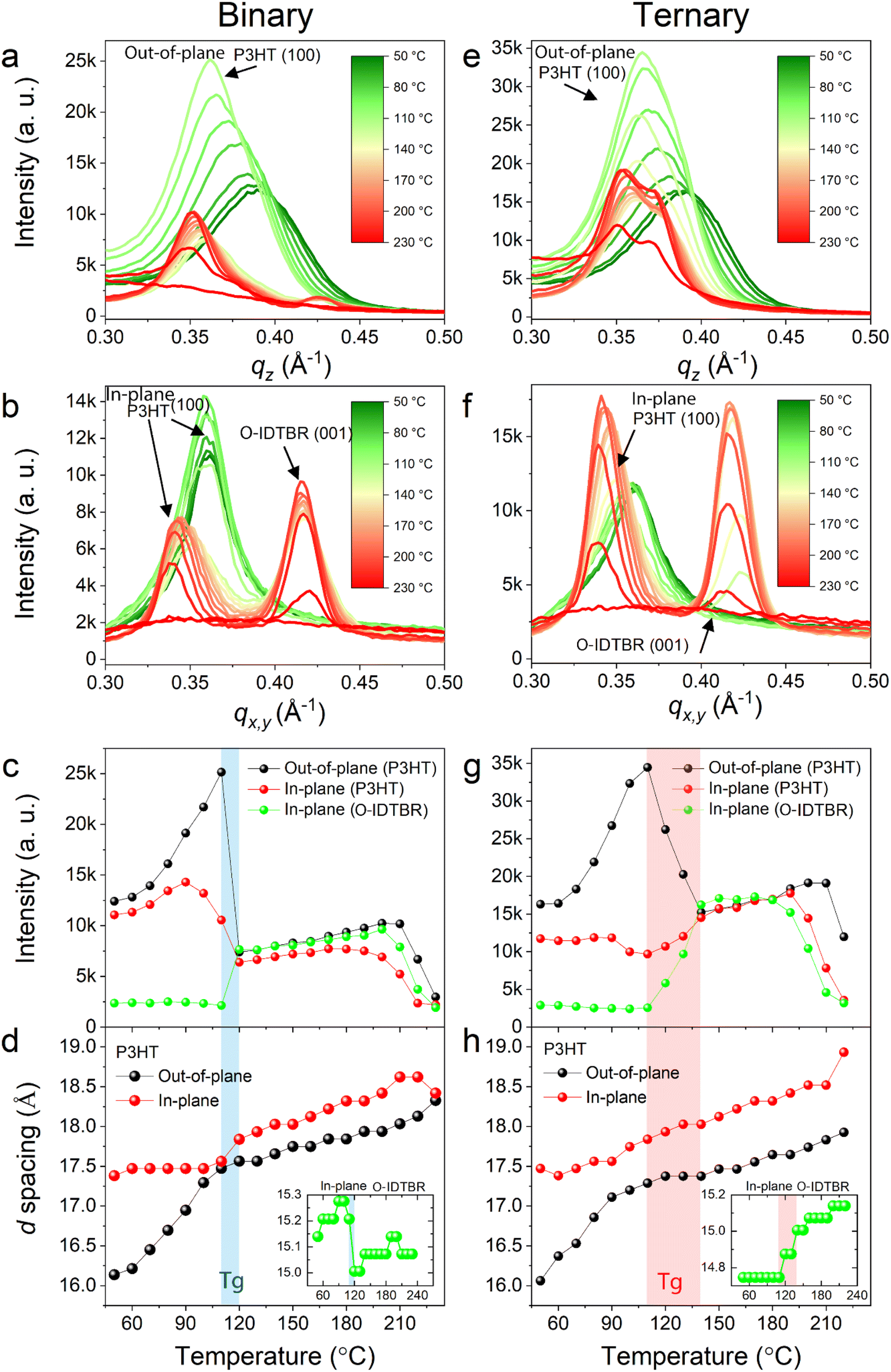 | ||
| Fig. 3 (a) and (b) Temperature-dependent one-dimensional (1-D) GIWAXS profiles of the binary blend along the OOP and IP directions, respectively. (c) and (d) Intensities and d spacings of the diffraction peaks for P3HT and O-IDTBR in the binary film along the OOP and IP directions. (e) and (f) Temperature-dependent one-dimensional (1-D) GIWAXS profiles of the ternary blend along the OOP and IP directions, respectively. (g) and (h) Intensities and d spacings of the diffraction peaks for P3HT and O-IDTBR in the binary film along the OOP and IP directions. The shaded areas in (c), (d), (g) and (h) represent the glass transitions for the binary (blue) and ternary (red) blends. | ||
At 50 °C, diffraction peaks of the P3HT (100) plane are observed at 0.361 Å−1 (d(100) = 2π/0.361 = 17.4 Å) and 0.391 Å−1 (d(100) = 16.1 Å) in IP and OOP profiles, respectively. These peaks correspond to lamellar packing of P3HT with face-on (IP peak) and edge-on (OOP peak) orientations. Additionally, the diffraction peak of the O-IDTBR (001) plane is predominantly observed in the IP profile at qx,y = 0.416 Å−1 (d(100) = 15.1 Å) at 50 °C, indicating that a face-on orientation is preferred for O-IDTBR but its intensity is extremely weak below 120 °C. We note that the O-IDFBR peaks do not appear in these measurements, consistent with the amorphous nature of this acceptor in thin films.36
The intensities and d-spacings of the diffraction peaks for P3HT and O-IDTBR in the binary film are plotted as a function of temperature to study their thermal stability (Fig. 3c and d). From 50 °C to 117 °C, the d-spacing of the IP P3HT peak remains constant, while its intensity slightly increases up to 90 °C, after which there is a significant drop in intensity until 120 °C. We suggest that this intensity drop is due to the glass transition at which the P3HT side chains becomes more mobile and less ordered, compared to the initial state.39 Above 120 °C, the intensity of the IP P3HT peak remains nearly constant, whereas its d spacing continually increases. Conversely, the OOP P3HT peak presents different features: its intensity is doubled and its d-spacing linearly increases as temperature increases from 50 °C to 117 °C. At 120 °C, the peak intensity of OOP P3HT abruptly drops but remains virtually constant with further temperature increases, while its d-spacing linearly increases at a slower rate with temperature. Moreover, at 120 °C, the peaks of the (001) O-IDTBR and acceptor π–π stacking appear at qx,y = 0.422 Å−1 (d(100) = 14.9 Å) and ∼1.6 Å−1 (dππ = 3.93 Å) in the IP direction, respectively, showing that the crystallinity of O-IDTBR is suddenly enhanced at this temperature with a favored face-on orientation. Finally, the two phases (P3HT and O-IDTBR) melt at 190–210 °C after which their intensities diminish.
The ternary blend X-ray peak changes with temeprature are similar to those of the binary blend, except for a few important distinctions (Fig. 3g and h). Unlike the binary blend, at lower temperatures (50–117 °C), the d-spacing of IP P3HT in the ternary blend gradually increases while its peak intensity remains virtually constant. The OOP P3HT peak behaves differently, with a significant increase in intensity and an increasing d-spacing up to 117 °C. Above 117 °C, three events take place – a large drop in the OOP P3HT peak intensity, a slight increase in the IP P3HT peak intensity and the appearance of the IP O-IDTBR peak. These trends continue up to 137 °C, demonstrating much broader OOP P3HT glass transition and O-IDTBR crystallization temepratures compared to the binary blend. These features can be related to an intermolecular interaction between O-IDFBR and IP P3HT, which inhibits the glass transition of IP P3HT and promotes the slow crystallization of O-IDTBR. Intriguingly, all of the three peaks in the ternary blend in this regime are higher than those in the binary blend by two-fold, indicating that the crystallinity of the ternary blend is superior to that of the binary blend. The two phases (P3HT and O-IDTBR) melt at a similar range of temperatures to those in the binary blend. We note that the GIWAXS data of the π–π stacking of the binary and ternary blends follow similar trends as those of the alkyl stacking (Fig. S7†) and all these results remain identical after cooling to room temperature, indicating that the changes in crystallinity are irreversible.
In situ STEM measurements during annealing
To comprehend how the temperature dependent molecular packing evolves at the nanoscale, we conducted temperature dependent in situ STEM at 25–160 °C. Fig. 4 shows a series of plan-view high-angle annular dark-field scanning TEM (HAADF-STEM) images of binary and ternary films obtained at four designated temperatures with insets of corresponding selected area electron diffraction (SAED) patterns. The binary and ternary films show no significant morphological differences at 50 °C (Fig. 4a and e) and the diffused rings in the SAED patterns show that these films are amorphous with no detectable long-range molecular ordering. As the temperature increases, a gradual increase in crystallinity (via molecular ordering) occurs in both films as proven by diffraction spots and their associated rings in the SAED patterns (see insets of Fig. 4b, c, d, f, g and h). Above 135 °C, the outermost ring pattern of both blends, which correspond approximately to P3HT and O-IDTBR becomes obvious as their π–π stacking distances are ∼3.80 and ∼3.65 Å, respectively (see Fig. S6†). Also, the contrast of the ring pattern of the ternary blend is stronger than that of the binary blend, indicating that the crystallinity of the two phases (P3HT and O-IDTBR) in the ternary blend is superior to that in the binary blend, in agreement with the GIWAXS results. We presume that other spots and rings in the patterns originate from the unexpected ordering of misaligned molecular stacks or formation of tiny polymorphs (that are not detectible in GIWAXS), and the diffraction spots from alkyl stacks are hidden due to the strong transmitted beam. | ||
| Fig. 4 A series of plan-view high-angle annular dark-field scanning TEM (HAADF-STEM) images of binary (a), (b), (c) and (d) and ternary films (e), (f), (g) and (h) obtained at the four designated temperatures (50 °C, 80 °C, 135 °C, and 160 °C) with the insets of the corresponding selected area electron diffraction (SAED) patterns. (i) and (j) Cross-sectional STEM images and electron dispersive spectroscopy (EDS) line profiles of the binary and ternary blends annealed at 135 °C, respectively. Each red dotted line indicates the position of the EDX line scan. | ||
Interestingly, large grains whose sizes are in a range of ∼2 μm are shown in the binary blend at 135 °C and the grains continue to grow up to 4 μm as the temperature increases to 160 °C due to grain coarsening (Fig. 4c and d). A larger view image reveals detailed morphologies of individual grains and the SAED pattern taken from a region 250 nm in diameter (the smallest aperture size) in a single grain (marked by a yellow circle) presents a signature of polycrystallinity, indicating that the grain is made up of many small domains of different phases of weakly-ordered molecules in a variety of orientations (Fig. S8†). However, the ternary blend features a fine-grained nanostructure with domains in the order of tens-of-nanometers and its morphological change is negligible with temperature, implying that the three phases (P3HT, O-IDTBR and O-IDFBR) in the film are randomly mixed and thermally stable (Fig. 4e–h).
To probe the composition throughout the depth of the film, the cross sections of the binary and ternary blend films annealed at 135 °C were examined using STEM and electron dispersive spectroscopy (EDS). The STEM image of the binary blend presents two vertically separated phases, identified by using two areas with different contrasts (Fig. 4i). The EDS line scan shows that the nitrogen contents of the two layers are different: 18% for the top layer (∼78 nm in thickness) versus 5% for the bottom layer (∼22 nm in thickness). The nitrogen in the blend is due to O-IDTBR, so the top layer is O-IDTBR rich, whilst the bottom layer is P3HT-rich. Differently, the image of the ternary blend shows a uniform contrast and the composition of nitrogen is constant throughout the blend, indicating that the phases of P3HT and O-IDTBR are homogeneously mixed (Fig. 4j). We note that the results shown above remain identical after cooling to room temperature, indicating that the phase and morphological changes are irreversible.
Models for phase stability of the two blends at elevated temperatures
From the in situ TEM and GIWAXS analyses discussed above, schematics illustrating the molecular-level structural evolution of binary and ternary blends during annealing (before melting) are proposed in Fig. 5. The phases in the binary blend change in the following way (Fig. 5a): at 50 °C, there are randomly orientated tiny domains of weakly crystallized IP and OOP P3HT phases and an amorphous O-IDTBR phase. At 90 °C, the crystallinity of P3HT is enhanced but O-IDTBR remains non-ordered, this is consistent with the increase in JSC and EQE for these devices, in which a more ordered polymer would have a higher absorption coefficient due to enhanced chain persistent lengths in the crystalline polymer.40 At 110–120 °C there is a sharp transition temperature at which IP and OOP P3HT crystallinities are reduced and IP O-IDTBR crystallinity sharply increases, forming domains with random orientations. These domains are grouped in large grains in which P3HT-rich and O-IDTBR-rich phases are vertically separated. Therefore, the enhanced JSC and reduced VOC of devices annealed at 125 °C result from the improved crystallinity of O-IDTBR which enhances both charge generation and transport. Above this transition temperature, the grains continue to grow, and this vertical phase separation is exacerbated, demonstrating an unstable morphology and resulting in a significant drop in device performance. For example, the difference in the nitrogen compositions of the separated layers at 160 °C becomes greater compared to that at 135 °C as shown in Fig. S9.† | ||
| Fig. 5 Detailed mechanism of the molecular-level structural evolution of (a) the binary and (b) ternary blend systems at the designated temperatures of 50 °C and 90 °C and above 120 °C. | ||
On the other hand, the phases in the ternary blend vary with the following sequence (Fig. 5b): at 50 °C, similar to the binary blend, there are randomly orientated tiny domains of weakly crystallized IP and OOP P3HT phases with amorphous acceptor phases. At 90 °C, only the crystallinity of OOP P3HT is enhanced with that of the other phases remaining constant. Unlike the binary blend, such an improvement in P3HT crystallinity results in a much improved JSC and EQE, resulting in improved charge generation from the more planar P3HT, and better charge transport. As the temperature increases further, there is a broad transition (110–140 °C) in which the crystallinity of OOP P3HT is reduced, crystallinity of IP P3HT is slightly improved and O-IDTBR crystallinity is dramatically improved. For the devices annealed at 135 °C, there is a significant improvement in the FF, suggesting improved charge extraction, likely coming from the better charge transport properties of the more crystalline acceptor, in conjunction with maintaining P3HT crystallinity due to the slower broad transition temperature. It is important to note that although O-IDTBR crystallinity is improved at this temperature (see Fig. 3g), there appear to be well mixed nanoscale domain distributions (see Fig. 4j). At temperatures above 140 °C, crystallinity of all three components is maintained and no large grains form, suggesting a much more stable morphology than the binary blend. This is evident in the temperature dependent device performance in which ternary devices annealed at 160 °C essentially maintain the performance of devices annealed at 135 °C.
Conclusions
Using in situ STEM, SAED, GIWAXS and EDX measurements, detailed information on the phase and morphology of the selected binary and ternary blends upon thermal annealing is attained and compared with the OPV device performance at the corresponding annealing temperatures. Tracking the intensities of both alkyl and π-stacking spectra from GIWAXS data is effective for quantitatively estimating the change in crystallinity at varied temperatures and comparing the crystallinities of the two blends. Moreover, STEM imaging combined with electron diffraction obtained at localized areas (from 250 nm to a few micrometers) and EDX analyses provide essential information on phase crystallinity, domain structure and phase separation. Such comprehensive information allows us to interpret the characteristics of the binary and ternary blend OPVs annealed at various temperatures. Our approach utilizing multiple in situ techniques is demonstrated to be a highly effective tool in optimizing the performance of polymer blend based OPVs by manipulating the crystallinity and morphology of the blend via thermal annealing. This provides us with key information on understanding the role of the third component in determining overall phase behavior, morphological stability, and device performance. Our results may extend to other ternary blends, particularly those that demonstrate improved morphological stability compared to their binary counterparts. In order to confirm the generality of our results it is important to apply similar in situ temperature dependent measurements to a variety of ternary systems, particularly the high efficiency blends incorporating the Y6 family of acceptors.Methods
Materials
High-purity electronic-grade semiconducting poly(3-hexyl thiophene) (P3HT) as a donor (∼98%) was synthesized by 1-Materials, Canada and was used as received. (5Z,5′Z)-5,5′-((7,7′-(4,4,9,9-Tetraoctyl-4,9-dihydro-s-indaceno[1,2-b:5,6-b′]dithiophene-2,7-diyl)bis(benzo[c][1,2,5]thiadiazole-7,4-diyl))bis(methanylylidene))bis(3-ethyl-2-thioxothiazolidin-4-one) (O-IDTBR) and 5,5′-[(6,12-dihydro-6,6,12,12-tetraoctylindeno[1,2-b]fluorene-2,8-diyl)bis(2,1,3-benzothiadiazole-7,4-diylmethylidyne)]bis[3-ethyl-2-thioxo-; (5Z,5′Z)-5,5′-((7,7′-(6,6,12,12-tetraoctyl-6,12-dihydroindeno[1,2-b]fluorene-2,8-diyl)bis(benzo[c][1,2,5]thiadiazole-7,4-diyl))bis(methanylylidene))bis(3-ethyl-2-thioxothiazolidin-4-one) (O-IDFBR) NFAs were synthesized by the McCulloch group at Imperial College London. To establish the binary and ternary system, we used a blend ratio of P3HT:O-IDTBR = 1:1 (w/w) and P3HT:O-IDTBR:O-IDFBR = 1:0.7:0.3 (w/w), respectively.36,41
Film characterization
The morphologies, and structural and chemical properties of the prepared samples were examined by using a field-emission transmission electron microscope (Tecnai G2 F30 S-Twin, 300 keV, FEI) equipped with a scanning transmission electron microscope (STEM) and energy dispersive X-ray spectrometer (EDS) using an in situ heating holder (model 652, Gatan). The plan-view samples were obtained by peeling the pre-deposited film (t ≈ 70 nm) from a glass substrate, and the films were transferred onto carbon-coated 200-mesh copper grids (Electron Microscopy Sciences). The cross-sectional samples (t ≈ 100 nm) were prepared by using the focused ion beam (FIB) milling technique.Structural analyses
In situ GIWAXS measurements were performed at the 3C-SAXSl beam line in the Pohang Accelerator Laboratory (PAL) using a monochromatized X-ray radiation source at an energy of 10.55 eV (λ = 0.117 nm) and a 2-D charge-coupled device (CCD) detector (Mar165 CCD). C8-BTBT rod samples were mounted onto a z-axis goniometer equipped with a vacuum chamber (≈10−3 Torr) and a Peltier plate, which provided excellent temperature accuracy along with a reliable cooling/heating rate (10 °C min−1). The samples were placed at a distance of 0.201 m from the CCD detector. The incident angle of each X-ray beam was set as 0.1°, and the scattering angles were determined from the positions of the X-ray beam reflected from the silicon substrate using pre-calibrated silver behenate. In situ scanning transmission electron microscopy (STEM) imaging and energy dispersive X-ray spectroscopy (EDS) measurements were performed using a high resolution transmission electron microscope (TEM, Tecnai™ G2, F30 S-Twin, operating at 80–300 keV, FEI) which was equipped with an in situ heating holder (652 double tilt, Gatan).Device and film preparation
ITO-coated glass substrates with a sheet resistance of ∼15 ohm per square were cleaned by sequentially ultrasonicating the material with detergent, deionized water, acetone, and isopropanol. Subsequently, the material was dried for 1 hour in an oven. A 125 mg mL−1 solution of zinc acetate dehydrate (Zn(OAc)2·2H2O, Sigma-Aldrich) in methanol, was spin coated on an ITO substrate at 2500 rpm for 60 s, followed by annealing at 200 °C for 10 min to obtain a ZnO layer with a thickness of 80 nm. A solution of P3HT:O-IDTBR (1:1) or P3HT:O-IDTRBR:O-IDFBR (1:0.7:0.3) in chlorobenzene with a concentration of 1 wt% was spin-cast on top of the ITO/ZnO layer in the clean room. The resulting BHJ film with a thickness of ∼100 nm was dried at 50, 80, 135, or 160 °C for 10 min. Finally, a MoOx (10 nm)/Ag (70 nm) electrode was thermally deposited under vacuum (10−7 Torr; 1 Torr ∼ 133 Pa) on top of the BHJ layer.
Calibration and device characterization
The spectrum obtained from the xenon (Xe) lamp (300 W Oriel) of a solar simulator was calibrated using a calibrated standard silicon solar cell with a protective window comprising KG5 filter glass produced by the National Renewable Energy Laboratory (NREL). The current–voltage (J–V) characteristics of the devices were measured using a Keithley 236 SMU, and simulated 100 mW cm−2 sunlight from the calibrated Xe lamp was employed. In the measurements, an AM 1.5-G filter was utilized under a N2 atmosphere.Conflicts of interest
The authors declare no conflict of interests.Acknowledgements
J. L. and Y. J. contributed equally to this work. We thank Dr Andrew Wadsworth and Prof. Iain McCulloch for providing the non-fullerene acceptor materials. This work was supported by the National Research Foundation of Korea (NRF) grant funded by the Korea government (MSIT) (No. NRF-2021R1A2C4001904 and No. NRF-2021R1A2C1005741). J. L. and J. S. K. would also like to acknowledge funding from the Global Research Laboratory Program of the NRF funded by MSIT (NRF-2017K1A1A2013153), and additionally the UK EPSRC for funding through both the ATIP Programme Grant (EP/T028513/1), and the Plastic Electronics Centre for Doctoral Training (EP/L016702/1).References
- C. Li, J. Zhou, J. Song, J. Xu, H. Zhang, X. Zhang, J. Guo, L. Zhu, D. Wei, G. Han, J. Min, Y. Zhang, Z. Xie, Y. Yi, H. Yan, F. Gao, F. Liu and Y. Sun, Nat. Energy, 2021, 6, 605 CrossRef CAS.
- N. Chaturvedi, N. Gasparini, D. Corzo, J. Bertrandie, N. Wehbe, J. Troughton and D. Baran, Adv. Funct. Mater., 2021, 31, 2009996 CrossRef CAS.
- L. Ma, S. Zhang, J. Wang, Y. Xu and J. Hou, Chem. Commun., 2020, 56, 14337 RSC.
- S. Dong, T. Jia, K. Zhang, J. Jing and F. Huang, Joule, 2020, 4, 2004 CrossRef CAS.
- S. Jeong, B. Park, S. Hong, S. Kim, J. Kim, S. Kwon, J. H. Lee, M. S. Lee, J. C. Park, H. Kang and K. Lee, ACS Appl. Mater. Interfaces, 2020, 12, 41877 CrossRef CAS.
- Q. Kang, L. Ye, B. Xu, C. An, S. J. Stuard, S. Zhang, H. Yao, H. Ade and J. Hou, Joule, 2019, 3, 227 CrossRef CAS.
- R. Xue, J. Zhang, Y. Li and Y. Li, Small, 2018, 14, 1801793 CrossRef PubMed.
- M. Riede, D. Spoltore and K. Leo, Adv. Energy Mater., 2021, 11, 2002653 CrossRef CAS.
- Y. Lin, M. I. Nugraha, Y. Firdaus, A. D. Scaccabarozzi, F. Aniés, A. H. Emwas, E. Yengel, X. Zheng, J. Liu, W. Wahyudi, E. Yarali, H. Faber, O. M. Bakr, L. Tsetseris, M. Heeney and T. D. Anthopoulos, ACS Energy Lett., 2020, 5, 3663 CrossRef CAS.
- J. Yuan, Y. Zhang, L. Zhou, G. Zhang, H. L. Yip, T. K. Lau, X. Lu, C. Zhu, H. Peng, P. A. Johnson, M. Leclerc, Y. Cao, J. Ulanski, Y. Li and Y. Zou, Joule, 2019, 3, 1140 CrossRef CAS.
- Q. Liu, Y. Jiang, K. Jin, J. Qin, J. Xu, W. Li, J. Xiong, J. Liu, Z. Xiao, K. Sun, S. Yang, X. Zhang and L. Ding, Sci. Bull., 2020, 65, 272 CrossRef CAS.
- Y. Chen, T. Liu, L. K. Ma, W. Xue, R. Ma, J. Zhang, C. Ma, H. K. Kim, H. Yu, F. Bai, K. S. Wong, W. Ma, H. Yan and Y. Zou, J. Mater. Chem. A, 2021, 9, 7481 RSC.
- Y. Wang, L. Yan, G. Ji, C. Wang, H. Gu, Q. Luo, Q. Chen, L. Chen, Y. Yang, C. Q. Ma and X. Liu, ACS Appl. Mater. Interfaces, 2019, 11, 2243 CrossRef CAS PubMed.
- C. Wang, S. Ni, S. Braun, M. Fahlman and X. Liu, J. Mater. Chem. C, 2019, 7, 879 RSC.
- J. Wei, G. Ji, C. Zhang, L. Yan, Q. Luo, C. Wang, Q. Chen, J. Yang, L. Chen and C. Q. Ma, ACS Nano, 2018, 12, 5518 CrossRef CAS.
- Y. Lin, Y. Firdaus, F. H. Isikgor, M. I. Nugraha, E. Yengel, G. T. Harrison, R. Hallani, A. El-Labban, H. Faber, C. Ma, X. Zheng, A. Subbiah, C. T. Howells, O. M. Bakr, I. McCulloch, S. De Wolf, L. Tsetseris and T. D. Anthopoulos, ACS Energy Lett., 2020, 5, 2935 CrossRef CAS.
- Y. Cai, L. Chang, L. You, B. Fan, H. Liu and Y. Sun, ACS Appl. Mater. Interfaces, 2018, 10, 24082 CrossRef CAS.
- R. Zhou, Z. Jiang, C. Yang, J. Yu, J. Feng, M. A. Adil, D. Deng, W. Zou, J. Zhang, K. Lu, W. Ma, F. Gao and Z. Wei, Nat. Commun., 2019, 10, 1 CrossRef CAS.
- W. Zhao, S. Zhang, Y. Zhang, S. Li, X. Liu, C. He, Z. Zheng and J. Hou, Adv. Mater., 2018, 30, 1704837 CrossRef.
- Z. Zhou, W. Liu, G. Zhou, M. Zhang, D. Qian, J. Zhang, S. Chen, S. Xu, C. Yang, F. Gao, H. Zhu, F. Liu and X. Zhu, Adv. Mater., 2020, 32, 1906324 CrossRef CAS PubMed.
- K. Weng, L. Ye, L. Zhu, J. Xu, J. Zhou, X. Feng, G. Lu, S. Tan, F. Liu and Y. Sun, Nat. Commun., 2020, 11, 1 CrossRef.
- F. Liu, L. Zhou, W. Liu, Z. Zhou, Q. Yue, W. Zheng, R. Sun, W. Liu, S. Xu, H. Fan, L. Feng, Y. Yi, W. Zhang and X. Zhu, Adv. Mater., 2021, 33, 2100830 CrossRef CAS.
- H. Meng, C. Liao, M. Deng, X. Xu, L. Yu and Q. Peng, Angew. Chem., Int. Ed., 2021, 60, 22554 CrossRef CAS.
- Y. Cai, Y. Li, R. Wang, H. Wu, Z. Chen, J. Zhang, Z. Ma, X. Hao, Y. Zhao, C. Zhang, F. Huang and Y. Sun, Adv. Mater., 2021, 33, 2101733 CrossRef CAS PubMed.
- P. Bi, S. Zhang, Z. Chen, Y. Xu, Y. Cui, T. Zhang, J. Ren, J. Qin, L. Hong, X. Hao and J. Hou, Joule, 2021, 5, 2408 CrossRef CAS.
- Y. Cui, Y. Xu, H. Yao, P. Bi, L. Hong, J. Zhang, Y. Zu, T. Zhang, J. Qin, J. Ren, Z. Chen, C. He, X. Hao, Z. Wei and J. Hou, Adv. Mater., 2021, 33, 2102420 CrossRef CAS.
- Z. Zhou, S. Xu, J. Song, Y. Jin, Q. Yue, Y. Qian, F. Liu, F. Zhang and X. Zhu, Nat. Energy, 2018, 3, 952 CrossRef CAS.
- T. Ameri, P. Khoram, J. Min and C. J. Brabec, Adv. Mater., 2013, 25, 4245 CrossRef CAS.
- B. V. K. Naidu, J. S. Park, S. C. Kim, S. M. Park, E. J. Lee, K. J. Yoon, S. Joon Lee, J. Wook Lee, Y. S. Gal and S. H. Jin, Sol. Energy Mater. Sol. Cells, 2008, 92, 397 CrossRef CAS.
- S. Honda, H. Ohkita, H. Benten and S. Ito, Chem. Commun., 2010, 46, 6596 RSC.
- D. H. Wang, K. H. Park, J. H. Seo, J. Seifter, J. H. Jeon, J. K. Kim, J. H. Park, O. O. Park and A. J. Heeger, Adv. Energy Mater., 2011, 1, 766 CrossRef CAS.
- J. Zhang, Y. Zhang, J. Fang, K. Lu, Z. Wang, W. Ma and Z. Wei, J. Am. Chem. Soc., 2015, 137, 8176 CrossRef CAS PubMed.
- W. Zhao, D. Qian, S. Zhang, S. Li, O. Inganäs, F. Gao and J. Hou, Adv. Mater., 2016, 28, 4734 CrossRef CAS PubMed.
- M. A. Pan, T. K. Lau, Y. Tang, Y. C. Wu, T. Liu, K. Li, M. C. Chen, X. Lu, W. Ma and C. Zhan, J. Mater. Chem. A, 2019, 7, 20713 RSC.
- Q. An, X. Ma, J. Gao and F. Zhang, Sci. Bull., 2019, 64, 504 CrossRef CAS.
- D. Baran, R. A. S. Ashraf, D. A. Hanifi, M. Abdelsamie, N. Gasparini, J. A. Röhr, S. Holliday, A. Wadsworth, S. Lockett, M. Neophytou, C. J. M. Emmott, J. Nelson, C. J. Brabec, A. Amassian, T. Kirchartz, J. R. Durrant, I. Mcculloch, D. Baran, R. A. S. Ashraf, S. Holliday, A. Wadsworth, S. Lockett and P. J. R. Durrant, Nat. Mater., 2016, 16, 363 CrossRef.
- S. Hong, J. Lee, H. Kang, G. Kim, S. Kee, J. H. Lee, S. Jung, B. Park, S. Kim, H. Back, K. Yu and K. Lee, Sci. Adv., 2018, 4, eaat3604 CrossRef CAS.
- A. J. Trindade and L. Pereira, Int. J. Photoenergy, 2017, 2017, 1364152 CrossRef.
- C. Müller, Chem. Mater., 2015, 27, 2740 CrossRef.
- M. S. Vezie, S. Few, I. Meager, G. Pieridou, B. Dörling, R. S. Ashraf, A. R. Goñi, H. Bronstein, I. McCulloch, S. C. Hayes, M. Campoy-Quiles and J. Nelson, Nat. Mater., 2016, 15, 746 CrossRef CAS.
- A. Harillo-Baños, X. Rodríguez-Martínez and M. Campoy-Quiles, Adv. Energy Mater., 2020, 10, 1902417 CrossRef.
Footnotes |
| † Electronic supplementary information (ESI) available. See DOI: https://doi.org/10.1039/d2ta07209b |
| ‡ J. L. and Y. J. contributed equally to this work. |
| This journal is © The Royal Society of Chemistry 2023 |