
 Open Access Article
 This Open Access Article is licensed under a Creative Commons Attribution-Non Commercial 3.0 Unported Licence
Indirect-to-direct bandgap transition in layered metal halide perovskite – CsPb2Br5†
Xiao
Wu
 a,
Xiangyu
Zhang
ab,
Wei
Yu
a,
Yongxiang
Zhou
ab,
Walter
Wong
a,
Weixin
He
a,
Kian Ping
Loh
a,
Xiao-Fang
Jiang
*c and
Qing-Hua
Xu
*ab
a,
Xiangyu
Zhang
ab,
Wei
Yu
a,
Yongxiang
Zhou
ab,
Walter
Wong
a,
Weixin
He
a,
Kian Ping
Loh
a,
Xiao-Fang
Jiang
*c and
Qing-Hua
Xu
*ab
aDepartment of Chemistry, National University of Singapore (NUS), 3 Science Drive 3, Singapore 117543, Singapore. E-mail: chmxqh@nus.edu.sg
bNUS (Suzhou) Research Institute, Suzhou 215123, China
cLaboratory of Quantum Engineering and Quantum Material, School of Physics and Telecommunication Engineering, South China Normal University, Guangzhou 510006, China. E-mail: jiangxf@scnu.edu.cn
First published on 25th January 2023
Abstract
All-inorganic layered halide perovskite CsPb2Br5 has many potential applications due to its interesting optical properties and long-term stability. However, its photoluminescence mechanism remains controversial due to the contradiction between its indirect bandgap nature and experimental observation of efficient green emission. The optical properties of CsPb2Br5 are highly dependent on the sample quality and preparation method, which is partially responsible for the controversy. Here, we prepared high-quality millimeter sized CsPb2Br5 single crystals using a saturated solvent evaporation crystallization method. The non-emissive CsPb2Br5 single crystals were found to convert into highly efficient green emitters with emission enhancement of up to four orders of magnitude by a simple thermal annealing process or irradiation with UV light or femtosecond laser pulses via multi-photon absorption. Through comprehensive characterization studies and theoretical calculations, a mechanism of the thermally induced indirect-to-direct bandgap transition associated with defect formation was proposed to explain the dramatic change in the optical properties of CsPb2Br5.
1 Introduction
Metal halide perovskites (MHPs) have found a wide range of applications in solar cells,1,2 light-emitting diodes,3–6 photodetectors,7,8 and lasers9–11 owing to their intriguing optoelectronic properties such as large absorption coefficients, high photoluminescence (PL) quantum efficiencies and long carrier diffusion lengths.12,13 CsPb2Br5, a novel layered MHP with a quasi-2D structure, displays interesting optoelectronic properties with a lot of potential applications10,14,15 thanks to its excellent water resistance and long-term chemical stability compared to traditional MHPs such as CsPbBr3.16–18 However, the PL mechanism of CsPb2Br5 remains highly controversial.19–23 Theoretical calculations predicted that CsPb2Br5 is an indirect bandgap semiconductor and should be PL-inactive,23,24 which is supported by some experimental results.24,25 However, CsPb2Br5 nanocrystals,26–28 microplates,10 and films14,17 have been found to display strong green emissions and can act as promising candidates for light-emitting diodes and laser devices. Several mechanisms have been proposed to explain this controversy, such as the emissive CsPbBr3 impurity,19,22,29 surface defects composed of different amorphous lead bromide ammonium complexes,21 and intrinsic defects in the CsPb2Br5 crystal lattice induced by the synthesis process.23 The optical properties of CsPb2Br5, similar to those of other MHPs,30,31 have been found to strongly depend on the sample quality and preparation method.19,20,25,26 For example, CsPb2Br5 prepared by a hot-injection method, in which the CsPbBr3 phase was an intermediate, displayed strong green emission primarily arising from the embedded CsPbBr3 phase.19,22,25 Preparation of high-quality CsPb2Br5 single crystals (SCs) is critical for understanding their intrinsic optical properties to explore their potential optoelectronic applications.High-quality CsPb2Br5 SCs have been previously synthesized using an anti-solvent vapor crystallization (AVC) method.24 The AVC method relies on diffusion of methanol (anti-solvent) into dimethyl sulfoxide solvent to initiate nucleation, which is very time-consuming and may take up to a few weeks. The saturated solvent evaporation crystallization (SSEC) method, which is known to be timesaving, straightforward, and highly repeatable, has been successfully utilized to prepare high-quality organic–inorganic hybrid and all-inorganic MHPs such as MAPbI3 (ref. 32) and CsPbBr3.33 Given the good solubility of PbBr2 and CsBr in HBr solution and excellent volatility of HBr, the SSEC method could be a good alternative for synthesizing CsPb2Br5 SCs.
Herein, we have successfully synthesized high-quality CsPb2Br5 SCs with a size of up to 2 × 2 × 0.5 mm within 6 hours using the SSEC method. The high quality of the prepared CsPb2Br5 SCs allowed us to fully investigate their intrinsic optical properties. A simple thermal annealing treatment was found to result in conversion of CsPb2Br5 SCs from PL-inactive materials to efficient green light emitters. Comprehensive investigation and characterization suggest a mechanism of indirect-to-direct bandgap transition associated with thermally induced defects, which was also verified by theoretical first-principles calculations. The PL inactive-to-active transition of CsPb2Br5 SCs has also been activated by photothermal effects by using UV light irradiation or femtosecond (fs) laser pulses via three-photon-absorption. This unique thermally driven indirect-to-direct bandgap transition allows remarkable optoelectronic tunability of CsPb2Br5, facilitating its potential applications in anti-counterfeiting, micro–nano light fabrication, and information storage.
2 Experimental section
2.1 Preparation of CsPb2Br5 single crystals
1 mmol cesium bromide (CsBr, 99.99%, Sigma-Aldrich), 2 mmol lead(II) bromide (PbBr2, ≥98%, Sigma-Aldrich), and 10 mL of hydrobromic acid (HBr, 48 wt% in H2O, ≥99.99%, Sigma-Aldrich) were mixed in a round-bottomed flask and subsequently heated at 100 °C under magnetic stirring for 2 hours until the solution gradually became transparent. The reaction mixture was then quickly transferred to a Petri dish. Upon gradually cooling the mixture solution and evaporation of the HBr solvent, CsPb2Br5 SCs gradually nucleated and grew to 2 × 2 × 0.5 mm within 6 hours. CsPb2Br5 SCs were annealed using a DHG-9055A hot air-drying oven.2.2 Characterization of pristine and annealed CsPb2Br5 single crystals
Absorption spectra were measured on a UV-vis spectrophotometer (UV3600, SHIMANZU). Photoluminescence (PL) and photoluminescence excitation (PLE) spectra were measured on a HORIBA FluoroMax-4 spectrofluorometer. The XRD patterns were collected using a Bruker-AXS D8 Advance X-ray diffractometer with Cu-Kα (λ = 1.5418 Å) in the 2θ range of 10°–70° with a step size of 0.02° and a time setting of 0.05 s per step. Transmittance electron microscopy (TEM) and high-resolution TEM (HR-TEM) measurements were conducted in a high vacuum at 7 × 10⁻⁷ torr using an FEI Titan 80–300 with a beam voltage of 15 and 200 kV for TEM and HRTEM, respectively. CsPb2Br5 SCs were crushed into powder and then dispersed in cyclohexane before dropping onto an ultrathin carbon film supported copper grid (300 mesh) for TEM and HRTEM measurements. Scanning electron microscopy (SEM) and energy dispersive X-ray spectroscopy (EDS) were conducted in a high vacuum at 9 × 10⁻⁵ Pa using a JEOL JSM-6701f with beam voltages of 5 and 15 kV for SEM and EDS, respectively. CsPb2Br5 SCs for SEM and EDS measurements were transferred to a SiO2/Si substrate followed by a 10 nm Pt spray treatment. In situ X-ray photoelectron spectroscopy (XPS) measurement was performed using a SPECS system with an XR-50 X-ray Mg Kα (1253.7 eV) source. The sample was grown on a SiO2/Si substrate and annealed at 200 °C in a chamber with a vacuum pressure of 5.0 × 10⁻¹⁰ mbar. Data were collected separately at annealing times of 15, 30, and 60 min. Time-resolved photoluminescence (TRPL) decay profiles were measured on a HORIBA Fluorolog system under excitation at 375 nm using a NanoLED. The emission signals were detected using an R928P PMT and processed using a time-correlated single photon-counting (TCSPC) system.2.3 First-principles calculations
DFT calculations were performed using the Vienna ab initio simulation package (VASP), followed by data processing with the VASPKIT code.34 The projector augmented wave (PAW) pseudopotentials were used, and the Perdew–Burke–Ernzerhof (PBE) functional of the generalized gradient approximation (GGA) was chosen as an exchange–correlation functional. Note that accurate bandgap calculations require using hybrid functionals (e.g., HSE06). Since we are mainly concerned with the changes in the DOS and band structure of CsPb2Br5 before and after annealing and are limited by computational power, only PBE functional was used in this work. The perfect and defective 2 × 2 × 2 supercells were modeled with Materials Studio 2019. We set a 2 × 2 × 1 Monkhorst–Pack (MP) grid in the first Brillouin zone integrations for geometry optimization. The energy cutoff was set to 320 eV. Four high-symmetric k-points were set for band structure calculations, including: P (1/4, 1/4, 1/4), N (0, 1/2, 0), Γ (0, 0, 0), and M (1/2, 1/2, −1/2). The atoms were relaxed until the energy converged to less than 10−5 eV and the absolute values of maximum force on atoms were less than 0.02 eV Å−1. VESTA was employed to display all crystal structures, and the post-processing VASPKIT code was used to deal with the VASP calculation data.2.4 Laser writing and reading
Laser writing and reading processes and multi-photon absorption measurements were carried out on a homemade microscope imaging system (Fig. S1†) combined with an fs laser. A mode-locked Ti:sapphire laser (Chameleon Ultra II, Coherent) gave output laser pulses with a central wavelength of 800 nm, a repetition rate of 80 MHz, and a pulse duration of 140 fs. The femtosecond laser beam was focused onto the samples using a 50× objective lens (N.A. = 0.3) with a focus radius of ∼1 μm. The emission signals of the samples were collected using the same objective lens and passed through a bundled optical fiber to a monochromator (Acton, Spectra Pro 2300i) coupled with a CCD (Princeton Instruments, Pixis 100B). Laser writing was performed in line sweep mode on a PInano® XYZ Piezo System at a line sweep speed of 1 μm s−1. Laser reading was performed using a square sweep mode for five focus planes. The laser intensities used for laser writing and reading were 3 mJ cm−2 and 0.08 mJ cm−2, respectively.3 Results and discussion
The single crystals (SCs) studied in this work were prepared by a facile and easily reproducible SSEC method as shown in Fig. 1a. The detailed synthesis procedures are described in the Experimental section. Precession images (Fig. S2a†) derived from single crystal XRD (SC-XRD) measurements demonstrate that the pristine SCs were pure single crystals with no signs of additional phase or twinning, matching well with the tetragonal CsPb2Br5 phase with an I4/mcm space group. The R1 value for single crystal structure refinement is as low as 2.2%. The powder XRD results are consistent with the SC-XRD results. The XRD pattern of the pristine SC-powder matches well with that of tetragonal phase CsPb2Br5 (JCPDS no. 25-0211) without diffraction peaks corresponding to other phases (Fig. 2a). The obtained pristine CsPb2Br5 SCs were transparent under daylight and non-emissive under ultraviolet (UV) light illumination (Fig. 1b(i and ii)). The non-emissive properties are consistent with the intrinsic indirect bandgap nature of CsPb2Br5, which also confirms the high purity of the obtained CsPb2Br5 SCs. The pristine CsPb2Br5 SCs displayed strong absorption in the UV range with an onset at 365 nm (Fig. 1d). An indirect bandgap of 3.4 eV was obtained by using the Tauc method (Fig. S3†),35,36 which is in good agreement with the result obtained from density functional theory (DFT) calculations (3.41 eV).23 | ||
| Fig. 1 (a) Schematic diagram of the synthesis of CsPb2Br5 SCs. (b) Photographs of CsPb2Br5 SCs before (i and ii) and after (iii and iv) thermal annealing under daylight (i and iii) and UV light illumination (ii and iv); the scale bar is 4 mm. (c) PL intensity contour mapping of CsPb2Br5 SCs after thermal annealing at different temperatures for different time periods; λex = 375 nm. (d and e) Absorption (d) and fluorescence (e) spectra of CsPb2Br5 SCs before and after annealing treatment. The annealing condition in (b), (d), and (e) is 150 °C for 8 h. | ||
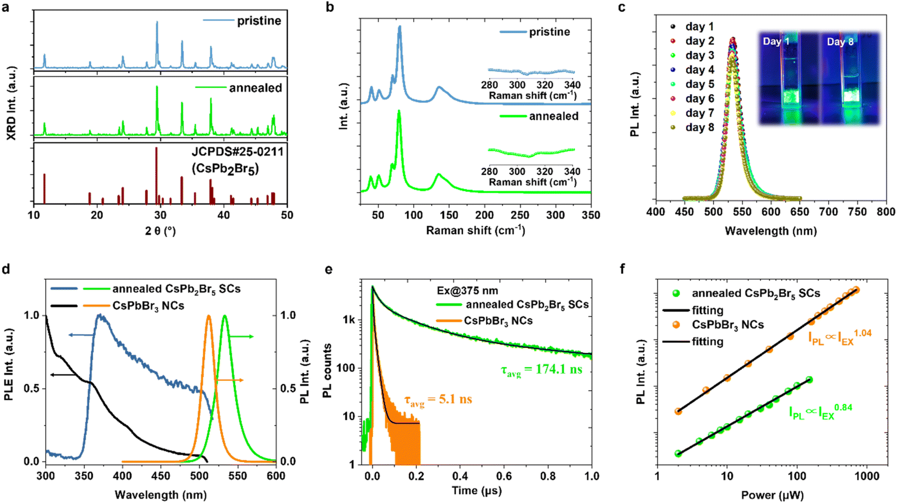 | ||
| Fig. 2 (a) Powder-XRD patterns of CsPb2Br5 SCs before and after annealing at 150 °C for 8 h. (b) Raman spectra of the pristine and annealed CsPb2Br5 SCs. (c) PL spectra of the annealed CsPb2Br5 SCs after immersion in water for 8 days. Insets show photographs of the annealed CsPb2Br5 SCs under UV light excitation on day 1 and day 8. (d) PL and PLE spectra of the annealed CsPb2Br5 SCs and CsPbBr3 NCs. (e) TRPL decay curves of the annealed CsPb2Br5 SCs and CsPbBr3 NCs. (f) Power dependent emission intensities of the annealed CsPb2Br5 SCs and CsPbBr3 NCs. | ||
It is interesting to observe that the PL-inactive pristine CsPb2Br5 SCs became PL-active after a simple thermal annealing treatment (Fig. 1b, c and e). Fig. 1b shows photographs of the annealed CsPb2Br5 SCs under daylight (iii) and UV light (iv) illumination after annealing at 150 °C for 8 h. The annealed CsPb2Br5 SCs appeared yellow under daylight and emitted strong green light under UV light illumination. Fig. 1c and S4† show the PL intensity contour mapping and the corresponding PL spectra of CsPb2Br5 SCs after thermal annealing treatment at different temperatures for different times. Effective conversion was observed at an annealing temperature above 100 °C. The optimum PL emission was achieved under annealing at 150 °C for 8 h with the integrated intensity enhanced by a factor of 11![[thin space (1/6-em)]](https://www.rsc.org/images/entities/char_2009.gif) 000. Further annealing resulted in a reduction in PL intensities. For annealing temperatures higher than 200 °C, the PL intensity reached the optimum within two hours and quickly decreased with prolonged annealing. Fig. 1d shows that the absorption spectrum of the annealed CsPb2Br5 SCs (150 °C, 8 h) was distinctly different from that of the pristine sample. Although both pristine and thermally annealed CsPb2Br5 SCs displayed strong absorption in the UV range, the annealed CsPb2Br5 SCs exhibited an additional absorption shoulder from 365 to 515 nm, suggesting a reconfiguration of the electronic structure. Under excitation at 375 nm, the annealed CsPb2Br5 SCs displayed a strong green light emission peaking at 534 nm with a corresponding PL quantum yield (PLQY) of 32%, in striking contrast with the extremely weak emission from the pristine CsPb2Br5 SCs (Fig. 1e).
000. Further annealing resulted in a reduction in PL intensities. For annealing temperatures higher than 200 °C, the PL intensity reached the optimum within two hours and quickly decreased with prolonged annealing. Fig. 1d shows that the absorption spectrum of the annealed CsPb2Br5 SCs (150 °C, 8 h) was distinctly different from that of the pristine sample. Although both pristine and thermally annealed CsPb2Br5 SCs displayed strong absorption in the UV range, the annealed CsPb2Br5 SCs exhibited an additional absorption shoulder from 365 to 515 nm, suggesting a reconfiguration of the electronic structure. Under excitation at 375 nm, the annealed CsPb2Br5 SCs displayed a strong green light emission peaking at 534 nm with a corresponding PL quantum yield (PLQY) of 32%, in striking contrast with the extremely weak emission from the pristine CsPb2Br5 SCs (Fig. 1e).
It has been previously shown that non-emissive CsPb2Br5 could convert to green-emitting CsPbBr3 at high temperatures (>400 °C).29,37 We indeed observed the conversion of CsPb2Br5 SCs to CsPbBr3 under annealing at 400 °C (Fig. S5†), resulting from melt-recrystallization of CsPb2Br5 SCs. However, the results obtained under annealing at 400 °C are totally different from those obtained under moderate thermal annealing conditions (<250 °C) as in our current work. The precession images of annealed CsPb2Br5 SCs (150 °C, 8 h) (Fig. S2b†) derived from SC-XRD measurement were almost identical to those of pristine CsPb2Br5 SCs (Fig. S2a†), indicating that the single crystal structure of CsPb2Br5 did not change after 150 °C annealing. The only difference in SC-XRD is the slight increase in the R1 value from 2.2% to 3.2% after thermal annealing, indicating reduced crystal quality after thermal annealing. The decreased crystallinity caused by thermal annealing was also supported by the powder XRD results as shown in Fig. S2c.† The full width at half maximum (FWHM) of the diffraction peak (002) located at 11.75° gradually increased from 0.067 to 0.136 as the annealing time gradually increased from 0 to 8 h at 150 °C. However, the powder XRD results showed no change in the overall XRD pattern and no additional diffraction peaks (Fig. 2a and S2c†) after thermal annealing, suggesting that the overall crystal structure of CsPb2Br5 did not change after thermal annealing at 150 °C, in agreement with the SC-XRD results. CsPb2Br5 SCs also displayed identical powder-XRD patterns to pristine CsPb2Br5 even after thermal annealing treatments for 24 h at different temperatures (25–250 °C) (Fig. S6†). Rietveld refinement of powder XRD indicates that the thermal annealing of CsPb2Br5 SCs at 200 °C for 4 h did not produce any new phase (Fig. S7†). These XRD results prove that the mild thermal annealing treatment in our experiments (<250 °C) did not prominently change the crystal structure of CsPb2Br5. In addition to the XRD measurements, the Raman spectra of CsPb2Br5 SCs did not change significantly before and after thermal annealing (150 °C, 8 h) (Fig. 2b). The CsPbBr3 phase typically shows a characteristic Raman peak at 310 cm−1,22 which was not observed in both the pristine and annealed CsPb2Br5 SCs (Fig. 2b). Furthermore, both the transmission electron microscope (TEM) images of CsPb2Br5 SCs-powder before and after annealing treatment (150 °C, 8 h) did not show any nanocrystals embedded in the host CsPb2Br5 framework (Fig. S8a and b†). Only the cystal lattice planes corresponding to CsPb2Br5 were observed in the high-resolution TEM (HRTEM) images (Fig. S8c†). It is well known that CsPbBr3 is sensitive to humidity and will decompose easily in water, leading to PL quenching.38,39 However, the green emission of the annealed CsPb2Br5 SCs (150 °C, 8 h) retained 90% of the original intensity even after 8 days of immersion in water (Fig. 2c and S9†). These results indicate that the observed dramatic changes in UV and PL spectra under mild thermal annealing (<250 °C) did not result from possible conversion from CsPb2Br5 SCs to CsPbBr3.
As XRD measurements may not be sensitive enough to the trace amount of embedded nanocrystals in the host CsPb2Br5 crystal framework and TEM measurements may not reflect the overall characteristics, methods that are more sensitive to trace impurities are needed to investigate the annealed CsPb2Br5 SCs to clarify the controversy. PL excitation (PLE) spectroscopy is a sensitive optical technique that allows the detection of small amounts of emissive species. Pure CsPbBr3 NCs were also prepared and characterized under the same conditions for direct comparison. Fig. 2d shows that the PL and PLE spectra of the annealed CsPb2Br5 SCs were distinctly different from those of pure CsPbBr3 NCs. The PL peak of the annealed CsPb2Br5 SCs appeared at 534 nm versus 515 nm for CsPbBr3 NCs. PLE spectra show that the green light emission of the annealed CsPb2Br5 SCs primarily arises from the excitation in the 365–515 nm range, corresponding to the thermal annealing-induced new emissive species, with little contribution from the excitation with wavelengths shorter than 350 nm. The absorption spectra (Fig. S10†) and time-resolved PL (TRPL) decay curves (Fig. 2e) of the annealed CsPb2Br5 SCs and pure CsPbBr3 NCs were also distinctly different from each other. The absorption spectrum of CsPbBr3 NCs exhibited an excitonic resonance at ∼510 nm and strong absorption in the UV range associated with the transition to higher energy bands.40 In contrast, the absorption of annealed CsPb2Br5 SCs in the visible range appeared more like the Urbach tail caused by defects.41,42 The annealed CsPb2Br5 SCs displayed a much longer PL lifetime (174 ns) than CsPbBr3 NCs (5.1 ns) (Fig. 2e). The short PL lifetime of CsPbBr3 NCs is consistent with their origin of exciton emission with large oscillator strengths.43 The much longer PL lifetime of the annealed CsPb2Br5 SCs implies their defect origin. Point defects such as vacancies can be formed easily in the Cs–Pb–Br compounds due to low formation energies.44–46 These defect-induced energy levels are expected to locate near the conduction band (CB)/valence band (VB)44–46 and may form a new extended bandgap for the larger bandgap CsPb2Br5. Furthermore, the PL excitation power-dependencies are also different for the annealed CsPb2Br5 SCs and pure CsPbBr3 NCs (Fig. 2f and S11†). The slope of log–log plot of emission intensity against excitation power was 1.04 for pure CsPbBr3 NCs, consistent with the fact of the exciton origin of the PL.43,47 In contrast, the corresponding slope for the annealed CsPb2Br5 SCs was 0.84, suggesting a defect-related nature of the observed PL emission.48 These results demonstrate that the observed green emission in the annealed CsPb2Br5 SCs had totally different origins from that of CsPbBr3 NCs. The thermally induced CsPbBr3 NCs impurity phase, if present, played a minor role in the observed green emission of the annealed CsPb2Br5 SCs.
It is interesting to note that the annealed CsPb2Br5 SCs exhibited remarkable stability in the ambient atmosphere. No obvious changes were observed in the powder-XRD patterns (Fig. 3a) and absorption spectrum (Fig. 3b) after storage for up to 400 days in the ambient atmosphere, indicating no apparent sign of decomposition for CsPb2Br5 SCs. The PLQY of the annealed CsPb2Br5 SCs remained nearly unchanged before and after storage for 400 days (Fig. 3c). Unlike CsPbBr3, which can be easily decomposed in water, the excellent stability of CsPb2Br5 against moisture prevents its decomposition in the ambient atmosphere. The stability of CsPb2Br5 lies in its unique layered structure, in which the interionic forces between Cs+ and [Pb2Br5]− are stronger than the ion-dipole forces between Cs+ and H2O, allowing CsPb2Br5 to stay stable even after immersion into water. Based on the XRD measurement results, it was found that thermal annealing did not change the crystal structure of CsPb2Br5 SCs. Consequently, CsPb2Br5 SCs retained their layered structure and maintained excellent water stability to display stable photoluminescence. The excellent stability of the annealed CsPb2Br5 SCs suggests their potential applications in highly stable single-crystal optoelectronic devices.
 | ||
| Fig. 3 (a) Powder-XRD patterns of the annealed CsPb2Br5 SCs after exposure in the ambient atmosphere for 0/100/200/400 days; (b) Absorption spectra of annealed CsPb2Br5 SCs after exposure in the ambient atmosphere for 0/100/200/400 days; (c) PL spectra and the corresponding PLQYs of annealed CsPb2Br5 SCs after exposure in the ambient atmosphere for 0 and 400 days. | ||
To understand the thermal annealing induced change in the electronic structure of CsPb2Br5 SCs, in situ X-ray photoelectron spectroscopy (XPS) of CsPb2Br5 SCs was utilized to monitor the evolution of surface elements during thermal annealing (Fig. 4a, b and S12†). The binding energies of Cs 4d3/2, Cs 4d5/2, Br 3d3/2, Br 3d5/2, Pb 4f5/2, and Pb 4f7/2 of the pristine CsPb2Br5 SCs were 77.3, 75.1, 69.5, 68.4, 143.8, and 138.9 eV, respectively, consistent with a previous report.15 After annealing at 200 °C for 1 h, the intensities of Br (3d3/2 & 3d5/2) and Pb (4f5/2 & 4f7/2) decreased while those of Cs (4d3/2 & 4d5/2) increased. The decreased intensities of Pb and Br indicate the release of Pb and Br from the surface, leaving Pb vacancies (VPb), Br vacancies (VBr), and highly uncoordinated Pb2+ (Fig. 4a and b).49–52 These uncoordinated Pb2+ ions exhibit characteristics of metallic Pb, as manifested by the Pb0 shoulder at the lower binding energy side of Pb 4f (Fig. 4b).53,54 On the other hand, the increased intensity of Cs suggests that the Cs+ ions inside the crystal gradually moved to the surface after annealing, resulting in a new shoulder at the lower binding energy side of Cs 4d5/2 (Fig. 4a).55 The possible origin of this new shoulder due to metallic Cs0 can be excluded as metallic Cs0 has a higher binding energy than Cs+.56 In the XPS measurements, the position and shape of binding energy can be influenced by factors such as charge accumulation at interfaces and surface charge accumulation.57 The accumulation of Cs+ on the surface induced by thermal annealing could lead to generation of dipole fields and deviations in photoelectron energies, resulting in a new shoulder at the lower energy side.58 The decrease in the molar ratios of Br and Pb and increase in Cs were also supported by the data of SEM-energy dispersive X-ray spectroscopy (SEM-EDS) (Fig. S13†). The excess Cs+ tends to fill up the Pb vacancies due to electrostatic attraction, forming Cs–Pb anti-sites (CsPb). Furthermore, the binding energies of Cs, Pb, and Br were found to shift towards the higher energy side (Fig. 4a and b), suggesting that the crystal surface became more n-type after annealing,59,60 resulting from the formation of donor-like VBr defects. The ultraviolet photoemission spectroscopy (UPS) results showed that the Fermi level of the annealed CsPb2Br5 SCs shifted upward to near the CB after thermal annealing at 200 °C for 1 h (Fig. S14†), indicating that the crystal surface of the annealed CsPb2Br5 became more n-type. These results demonstrated that thermal annealing resulted in formation of a significant amount of surface defects (VBr and CsPb).
 | ||
| Fig. 4 (a and b) In situ XPS patterns of Cs, Br, and Pb elements during thermal annealing (200 °C, 1 h). (c) DOS of CsPb2Br5 with different defect concentrations. Defect concentrations of (CsPb and VBr) are marked in the upper left corner of each panel in cm−3. The VBM energy is set to 0 eV for convenience in comparison. (d and e) The charge density of perfect CsPb2Br5 at the CBM and VBM. (f and g) The charge density of defective CsPb2Br5 near the defect VBr and CsPb. Yellow represents charge distribution, and the iso-surface value is set to 0.001 e Å−3 for all four cases. | ||
These defects may alter the electronic structure of CsPb2Br5 and affect its optical properties. The influence of defects on the electronic structure of CsPb2Br5 was explored by conducting DFT calculations with the Vienna ab initio simulation package (VASP) code, followed by data post-processing with the VASPKIT code.34 Calculation details are described in the Experimental section. Fig. 4c shows the calculated projected density of states (DOS) of CsPb2Br5 with different defect concentrations of CsPb and VBr. The corresponding band structures are shown in Fig. S15.† For pristine CsPb2Br5 without any defect, the valence band maximum (VBM) consists of the hybridization of Br 4p and Pb 6s states; the conduction band minimum (CBM) mainly consists of Pb 6p states, resulting in a calculated bandgap of 3.1 eV (Fig. 4c, top panel). The calculated bandgap was smaller than the experimental value due to the limitation of the generalized gradient approximation (GGA) scheme in DFT calculations.61–63 Despite underestimating the bandgap, DFT calculations can demonstrate the trend of variation in the electronic structure of CsPb2Br5 with defect concentrations. After introducing a low concentration of CsPb and VBr (1017, 1017), defect energy levels appear at 0.35 eV above the VBM and 0.44 eV below the CBM, respectively. With a gradual increase in the defect concentration from (1017, 1017) to (4 × 10¹⁷, 1018), the localized defect energy levels progressively broaden and eventually evolve into two defect energy bands that extend into the original VB and CB (Fig. 4c). As the defect concentration increases, the evolution of the defect energy levels into defect energy bands is also reflected in band structures (Fig. S15†). Besides, the original CB tends to move downward and deeper with the increasing defect concentration (Fig. 4c), because defect-induced lattice disorder influences the original band structures. A similar trend has also been previously reported in the double perovskite Cs2AgBiBr6.64 High-temperature synthesis of Cs2AgBiBr6 induces more anti-site defects that can cause lattice disorder, resulting in a downward shift of the CB and a reduced bandgap.64 The presence of VBr and CsPb will therefore result in formation of two defect energy bands and the downward shift of the original CB, leading to a reduction in the bandgap of CsPb2Br5, which is responsible for the additional absorption shoulder in the 365–515 nm range of the annealed CsPb2Br5 SCs (Fig. 1d).
An impressive feature of this additional absorption shoulder is the dramatic increase of the absorption near the band edge with a factor of more than 200 within 0.1 eV photon energy (Fig. S16†). In contrast, the absorbance near the band edge of pristine CsPb2Br5 increases by a factor of only 30 within 0.4 eV. Such a dramatic increase in the absorbance slope near the band edge suggests a transition from an indirect to a direct bandgap.65,66 The absorbance near the band edge follows a very different formula for direct and indirect bandgap semiconductors (see details in the ESI†). Direct bandgap semiconductors show a dramatic increase in absorbance when photon energy is just above the bandgap. In contrast, the absorbance near the band edge increases slowly with photon energy for indirect bandgap semiconductors, followed by a speedy increase due to photon energy being high enough to allow direct optical absorption. The second signature of the indirect-to-direct bandgap transition of CsPb2Br5 SCs is the significant PL enhancement after thermal annealing. Due to the indirect bandgap nature of pristine CsPb2Br5 SCs, the radiative transition requires participation of phonons to satisfy momentum conservation, which is very inefficient with hardly detectable emission. In contrast, the PLQY of the annealed CsPb2Br5 SCs achieves 32%, suggesting that direct radiative transition occurs without phonon participation in the annealed CsPb2Br5 SCs. A similar indirect-to-direct bandgap transition induced significant PL enhancement of 104-fold was found in MoS2 undergoing a transition from the indirect bandgap of bulk MoS2 to the direct bandgap of monolayer MoS2.67 The third piece of evidence for the indirect-to-direct bandgap transition of CsPb2Br5 is variation of k-vectors of the CBM and VBM during the optical transition. The CBM and VBM of a direct bandgap have the same electron momentum (k-vector) in the first Brillouin zone, while the k-vectors of the CBM and VBM are different in indirect bandgaps. The k-vectors of the VBM (N) and CBM (Γ) of pristine CsPb2Br5 are different in k-space (Fig. S17a†), indicating its indirect bandgap nature. The square of the transition dipole moment (TMD2) for pristine CsPb2Br5 is zero at the VBM and CBM (Fig. S17c†), indicating that the direct optical transitions at the VBM and CBM are forbidden, consistent with the indirect bandgap nature of pristine CsPb2Br5. Fig. 4d and e show that the charge densities (wavefunctions) of pristine CsPb2Br5 at the VBM and CBM are also separated in real space and located around Br atoms and Pb atoms, respectively. In contrast, the VBM and CBM of the annealed (defective) CsPb2Br5 move to the same k-vector (N) (Fig. S17b†), suggesting a transition from the indirect bandgap of pristine CsPb2Br5 to a direct bandgap for CsPb2Br5 with a high concentration of defects. The moderate TMD2 value at the N point indicates that the direct optical transitions between the CBM and VBM become allowed (Fig. S17d†) in the defective CsPb2Br5. The charge density of the defective CsPb2Br5 enriches around the CsPb and VBr (Fig. 4f and g). The highly localized charge distribution enhances the wavefunction overlap between electrons and holes on the two defect states, thus promoting the radiative recombination between the electrons and holes, rationalizing the efficient green emission of the annealed CsPb2Br5 SCs.
Apart from thermal annealing treatment, the PL enhancement of CsPb2Br5 SCs can also be achieved by photothermal effects, including normal UV light and femtosecond (fs) laser irradiation-induced photothermal effects. Fig. 5a and S18† show that the UV light irradiation of CsPb2Br5 SCs with a 150 W xenon-lamp can gradually induce a green light emission, while the CsPb2Br5 SCs without UV light irradiation have no light emission. Powder XRD measurements showed no additional diffraction peaks corresponding to other phases after UV light irradiation (Fig. S18b†), consistent with the result of thermal annealing treatment. Water stability (Fig. S18c†) and time-resolved PL measurements (Fig. S18d†) were also performed on UV light irradiated CsPb2Br5 SCs. The PL of UV light irradiated CsPb2Br5 SCs was stable in water for 48 hours (Fig. S18c†). If the PL comes from the transformed CsPbBr3, it will be quickly quenched as CsPbBr3 is unstable in water. Besides, the UV light irradiated CsPb2Br5 SCs exhibited an average PL lifetime of 708 ns (Fig. S18d†), much longer than the PL lifetime of CsPbBr3 nanocrystals (5.1 ns), which also excludes the possibility of PL origin of the UV light irradiated CsPb2Br5 SCs due to CsPbBr3 nanocrystals. The fs laser irradiation can also activate the PL of CsPb2Br5 SCs due to the multi-photon absorption-induced photothermal effect (Fig. 5b). A microscopy system integrated with an fs laser system at 800 nm (Fig. S1†) was employed to initiate multi-photon absorption. Under irradiation with laser pulses at 800 nm, CsPb2Br5 SCs can be excited via three-photon absorption to emit very weak broadband emissions from 450 to 750 nm (Fig. S19a†). The excitation nature of three-photon-absorption can be verified by the slope of ∼3 for a log–log plot of the emission intensity versus the excitation power (Fig. S19b†). Fig. 5b and c show that under continuous irradiation with an 800 nm fs laser beam, green emission from CsPb2Br5 SCs appeared rapidly within the first few minutes and reached the optimum after 10 min with an enhancement of nearly four orders of magnitude, followed by a slight decrease in the emission intensity with further prolonged irradiation time. As the CsPb2Br5 SC under fs laser irradiation was localized at the area of submicron level, the fs laser irradiated sample is not suitable for XRD measurements. However, water stability and PL-lifetime measurements (Fig. S18e and f†) exclude the possibility of the laser induced conversion from CsPb2Br5 to CsPbBr3. The observed PL enhancement of CsPb2Br5 SCs induced by UV light and fs laser irradiation is believed to originate from the same mechanism as thermal annealing due to photothermal effects. Taking advantage of the significant emission enhancement and the sub-micron scale localized excitation of three-photon absorption, the fs-laser-induced PL enhancement of CsPb2Br5 SCs could be utilized to demonstrate data storage and anti-counterfeiting in a sub-micron size. As shown in Fig. 5d, customized patterns or information can be ‘written’ on a specific focal plane and ‘read’ only on the same focal plane. An example is shown in Fig. 5e. An ‘NUS’ pattern with a resolution of sub 1 μm was directly ‘written’ on a CsPb2Br5 SC using a focused fs laser pulse at 800 nm (3.0 mJ cm−2). The obtained pattern was read out by two-photon excitation fluorescence mapping with identical resolution under excitation with a weaker fs laser beam at 800 nm (0.08 mJ cm−2). The two-photon excitation nature of the emission from the irradiated CsPb2Br5 SC was verified by its nearly squared excitation power dependency (Fig. S19c and d†). The fluorescence mapping results became blurred significantly when the ‘reading’ plane moved away from the ‘writing’ plane for 5 μm and almost totally disappeared for 10 μm (Fig. 5d and e). This simple demonstration suggests potential applications of CsPb2Br5 SCs in 3D optical data storage, micro–nano light source fabrication, and optical anti-counterfeiting.
 | ||
| Fig. 5 PL spectral evolution of CsPb2Br5 SCs under irradiation with (a) 350 nm xenon-lamp (150 W) and (b) 800 nm fs laser pulses with a power intensity of 3 mJ cm−2; (c) evolution of integrated PL intensity (450–600 nm) versus the irradiation time under 800 nm fs laser irradiation; (d) schematic diagram of laser writing and reading, and the optical image of CsPb2Br5 SC used for laser writing and reading. (e) An ‘NUS’ pattern is ‘written’ using a 3 mJ cm−2 focused 800 nm fs pulsed laser at a specific focus plane (focus = 0 μm) and read out at different focus planes (from −10 to 10 μm) using a focused 0.08 mJ cm−2 800 nm fs pulsed laser. The scale bar (white line) is 5 μm. | ||
4 Conclusions
In summary, we have utilized a saturated solvent evaporation crystallization method to prepare millimeter sized high-quality layered perovskite CsPb2Br5, which was found to undergo PL-inactive-to-active transition under mild thermal annealing. The distinct changes in the optical properties of CsPb2Br5 SCs were confirmed to arise from thermally induced VBr and CsPb, as verified by XRD, XPS, SEM-EDS, and DFT calculations. These defects generate additional defect energy bands that extended from the VBM and CBM and make direct optical transitions possible, resulting in bandgap reduction and indirect-to-direct bandgap transition. A similar transition was also observed by photothermal effects by irradiation with UV light or femtosecond laser pulses via multi-photon absorption. Our findings provide new insights on understanding the optoelectronic properties of CsPb2Br5, which may facilitate its applications in anti-counterfeiting, micro–nano light sources, information storage, and optoelectronic devices.Author contributions
X. Wu and Prof. Q. H. Xu conceptualized the project. X. Wu designed the experiments. X. Wu and X. Zhang performed the experiments under the guidance of Prof. Q. H. Xu; W. Yu, W. Wong and W. He performed the experiments under the guidance of Prof. K. P. Loh. X. Wu drafted the manuscript with Prof. X. F. Jiang. Prof. Q. H. Xu revised the manuscript. All authors contributed to the analysis of the results.Conflicts of interest
There are no conflicts of interest to declare.Acknowledgements
This research was supported by financial support from the Ministry of Education, Singapore (MOE Tier 1 A-8000013-00-00 and Tier 2 2018-T2-1-119), and National Natural Science Foundation of China (Grant No. 62075065 and 51603069).References
- Z. Wu, A. Y. Alsalloum, O. F. Mohammed and O. M. Bakr, Joule, 2022, 6, 951–952 CrossRef.
- Q. Xiao, J. Tian, Q. Xue, J. Wang, B. Xiong, M. Han, Z. Li, Z. Zhu, H.-L. Yip and Z. a. Li, Angew. Chem., Int. Ed., 2019, 58, 17724–17730 CrossRef CAS PubMed.
- J. Song, J. Li, X. Li, L. Xu, Y. Dong and H. Zeng, Adv. Mater., 2015, 27, 7162–7167 CrossRef CAS PubMed.
- W. Mao, J. Zheng, Y. Zhang, A. S. R. Chesman, Q. Ou, J. Hicks, F. Li, Z. Wang, B. Graystone, T. D. M. Bell, M. U. Rothmann, N. W. Duffy, L. Spiccia, Y.-B. Cheng, Q. Bao and U. Bach, Angew. Chem., Int. Ed., 2017, 56, 12486–12491 CrossRef CAS PubMed.
- G. Zou, Z. Li, Z. Chen, L. Chu, H.-L. Yip and Y. Cao, Adv. Funct. Mater., 2021, 31, 2103219 CrossRef CAS.
- A. Dey, J. Ye, A. De, E. Debroye, S. K. Ha, E. Bladt and L. Polavarapu, ACS Nano, 2021, 15, 10775–10981 CrossRef CAS PubMed.
- Q. Ou, Y. Zhang, Z. Wang, J. A. Yuwono, R. Wang, Z. Dai, W. Li, C. Zheng, Z.-Q. Xu, X. Qi, S. Duhm, N. V. Medhekar, H. Zhang and Q. Bao, Adv. Mater., 2018, 30, 1705792 CrossRef PubMed.
- X. Li, C. Meng, B. Huang, D. Yang, X. Xu and H. Zeng, Adv. Opt. Mater., 2020, 8, 2000273 CrossRef CAS.
- G. Xing, N. Mathews, S. S. Lim, N. Yantara, X. Liu, D. Sabba, M. Grätzel, S. Mhaisalkar and T. C. Sum, Nat. Mater., 2014, 13, 476–480 CrossRef CAS PubMed.
- X. Tang, Z. Hu, W. Yuan, W. Hu, H. Shao, D. Han, J. Zheng, J. Hao, Z. Zang, J. Du, Y. Leng, L. Fang and M. Zhou, Adv. Opt. Mater., 2017, 5, 1600788 CrossRef.
- J. Yang, Z. Liu, M. Pi, H. Lin, F. Zeng, Y. Bian, T. Shi, J. Du, Y. Leng and X. Tang, Adv. Opt. Mater., 2020, 8, 2000290 CrossRef CAS.
- G. Xing, N. Mathews, S. Sun, S. L. Swee, M. L. Yeng, M. Grätzel, S. Mhaisalkar and C. S. Tze, Science, 2013, 342, 344–347 CrossRef CAS PubMed.
- Q. Wei, J. Yin, O. M. Bakr, Z. Wang, C. Wang, O. F. Mohammed, M. Li and G. Xing, Angew. Chem., Int. Ed., 2021, 60, 10957–10963 CrossRef CAS PubMed.
- C. Qin, T. Matsushima, A. S. D. Sandanayaka, Y. Tsuchiya and C. Adachi, J. Phys. Chem. Lett., 2017, 8, 5415–5421 CrossRef CAS PubMed.
- R. Wang, Z. Li, S. Li, P. Wang, J. Xiu, G. Wei, H. Liu, N. Jiang, Y. Liu and M. Zhong, ACS Appl. Mater. Interfaces, 2020, 12, 41919–41931 CrossRef CAS PubMed.
- G. Jiang, C. Guhrenz, A. Kirch, L. Sonntag, C. Bauer, X. Fan, J. Wang, S. Reineke, N. Gaponik and A. Eychmüller, ACS Nano, 2019, 13, 10386–10396 CrossRef CAS PubMed.
- G. Tong, H. Li, D. Li, Z. Zhu, E. Xu, G. Li, L. Yu, J. Xu and Y. Jiang, Small, 2018, 14, 1702523 CrossRef PubMed.
- B. Qiao, P. Song, J. Cao, S. Zhao, Z. Shen, G. Di, Z. Liang, Z. Xu, D. Song and X. Xu, Nanotechnology, 2017, 28, 445602 CrossRef PubMed.
- T. Zhang, Z. Chen, Y. Shi and Q.-H. Xu, Nanoscale, 2019, 11, 3186–3192 RSC.
- Y. Jiang, B. Li, T. Zhang, Y. Shi and Q.-H. Xu, ChemNanoMat, 2020, 6, 327–335 CrossRef CAS.
- P. Acharyya, P. Pal, P. K. Samanta, A. Sarkar, S. K. Pati and K. Biswas, Nanoscale, 2019, 11, 4001–4007 RSC.
- C. Wang, Y. Wang, X. Su, V. G. Hadjiev, S. Dai, Z. Qin, H. A. C. Benavides, Y. Ni, Q. Li, J. Jian, M. K. Alam, H. Wang, F. C. R. Hernandez, Y. Yao, S. Chen, Q. Yu, G. Feng, Z. Wang and J. Bao, Adv. Mater., 2019, 31, 1902492 CrossRef PubMed.
- Y.-Q. Zhou, J. Xu, J.-B. Liu and B.-X. Liu, J. Phys. Chem. Lett., 2019, 10, 6118–6123 CrossRef CAS PubMed.
- I. Dursun, M. De Bastiani, B. Turedi, B. Alamer, A. Shkurenko, J. Yin, A. M. El-Zohry, I. Gereige, A. AlSaggaf, O. F. Mohammed, M. Eddaoudi and O. M. Bakr, ChemSusChem, 2017, 10, 3746–3749 CrossRef CAS PubMed.
- G. Li, H. Wang, Z. Zhu, Y. Chang, T. Zhang, Z. Song and Y. Jiang, Chem. Commun., 2016, 52, 11296–11299 RSC.
- K.-H. Wang, L. Wu, L. Li, H.-B. Yao, H.-S. Qian and S.-H. Yu, Angew. Chem., Int. Ed., 2016, 55, 8328–8332 CrossRef CAS PubMed.
- J. Lv, L. Fang and J. Shen, Mater. Lett., 2018, 211, 199–202 CrossRef CAS.
- L. Ruan, W. Shen, A. Wang, A. Xiang and Z. Deng, J. Phys. Chem. Lett., 2017, 8, 3853–3860 CrossRef CAS PubMed.
- J. Li, H. Zhang, S. Wang, D. Long, M. Li, Y. Guo, Z. Zhong, K. Wu, D. Wang and T. Zhang, RSC Adv., 2017, 7, 54002–54007 RSC.
- C. Otero-Martínez, D. García-Lojo, I. Pastoriza-Santos, J. Pérez-Juste and L. Polavarapu, Angew. Chem., Int. Ed., 2021, 60, 26677–26684 CrossRef PubMed.
- C. Otero-Martínez, M. Imran, N. J. Schrenker, J. Ye, K. Ji, A. Rao, S. D. Stranks, R. L. Z. Hoye, S. Bals, L. Manna, J. Pérez-Juste and L. Polavarapu, Angew. Chem., Int. Ed., 2022, e202205617 Search PubMed.
- Q. Dong, Y. Fang, Y. Shao, P. Mulligan, J. Qiu, L. Cao and J. Huang, Science, 2015, 347, 967–970 CrossRef CAS PubMed.
- C. C. Stoumpos, C. D. Malliakas, J. A. Peters, Z. Liu, M. Sebastian, J. Im, T. C. Chasapis, A. C. Wibowo, D. Y. Chung, A. J. Freeman, B. W. Wessels and M. G. Kanatzidis, Cryst. Growth Des., 2013, 13, 2722–2727 CrossRef CAS.
- V. Wang, N. Xu, J.-C. Liu, G. Tang and W.-T. Geng, Comput. Phys. Commun., 2021, 267, 108033 CrossRef CAS.
- J. Tauc, R. Grigorovici and A. Vancu, Phys. Status Solidi B, 1966, 15, 627–637 CrossRef CAS.
- P. Makuła, M. Pacia and W. Macyk, J. Phys. Chem. Lett., 2018, 9, 6814–6817 CrossRef PubMed.
- G. Maity and S. K. Pradhan, J. Alloys Compd., 2020, 816, 152612 CrossRef CAS.
- K. Sandeep, K. Y. Gopika and M. R. Revathi, Phys. Status Solidi RRL, 2019, 13, 1900387 CrossRef CAS.
- B. Akbali, G. Topcu, T. Guner, M. Ozcan, M. M. Demir and H. Sahin, Phys. Rev. Mater., 2018, 2, 034601 CrossRef CAS.
- J. Aneesh, A. Swarnkar, V. K. Ravi, R. Sharma, A. Nag and K. V. Adarsh, J. Phys. Chem. C, 2017, 121, 4734–4739 CrossRef CAS.
- A. Meeder, D. F. Marrón, A. Rumberg, M. C. Lux-Steiner, V. Chu and J. P. Conde, J. Appl. Phys., 2002, 92, 3016–3020 CrossRef CAS.
- K. Boubaker, Eur. Phys. J. Plus, 2011, 126, 10 CrossRef.
- M. A. Becker, R. Vaxenburg, G. Nedelcu, P. C. Sercel, A. Shabaev, M. J. Mehl, J. G. Michopoulos, S. G. Lambrakos, N. Bernstein, J. L. Lyons, T. Stöferle, R. F. Mahrt, M. V. Kovalenko, D. J. Norris, G. Rainò and A. L. Efros, Nature, 2018, 553, 189–193 CrossRef CAS PubMed.
- J. Bao and V. G. Hadjiev, Nano-Micro Lett., 2019, 11, 26 CrossRef CAS PubMed.
- J. Yin, H. Yang, K. Song, A. M. El-Zohry, Y. Han, O. M. Bakr, J.-L. Brédas and O. F. Mohammed, J. Phys. Chem. Lett., 2018, 9, 5490–5495 CrossRef CAS PubMed.
- M. V. Kovalenko, L. Protesescu and M. I. Bodnarchuk, Science, 2017, 358, 745–750 CrossRef CAS PubMed.
- M. Gao, H. Liu, S. Yu, S. Louisia, Y. Zhang, D. P. Nenon, A. P. Alivisatos and P. Yang, J. Am. Chem. Soc., 2020, 142, 8871–8879 CrossRef PubMed.
- T. Schmidt, K. Lischka and W. Zulehner, Phys. Rev. B: Condens. Matter Mater. Phys., 1992, 45, 8989–8994 CrossRef PubMed.
- Y.-H. Seo, J. H. Kim, D.-H. Kim, H.-S. Chung and S.-I. Na, Nano Energy, 2020, 77, 105164 CrossRef CAS.
- G. Divitini, S. Cacovich, F. Matteocci, L. Cinà, A. Di Carlo and C. Ducati, Nat. Energy, 2016, 1, 15012 CrossRef CAS.
- E. Bi, H. Chen, F. Xie, Y. Wu, W. Chen, Y. Su, A. Islam, M. Grätzel, X. Yang and L. Han, Nat. Commun., 2017, 8, 15330 CrossRef CAS PubMed.
- M. Long, T. Zhang, M. Liu, Z. Chen, C. Wang, W. Xie, F. Xie, J. Chen, G. Li and J. Xu, Adv. Mater., 2018, 30, 1801562 CrossRef PubMed.
- W. Zhang, S. Pathak, N. Sakai, T. Stergiopoulos, P. K. Nayak, N. K. Noel, A. A. Haghighirad, V. M. Burlakov, D. W. deQuilettes, A. Sadhanala, W. Li, L. Wang, D. S. Ginger, R. H. Friend and H. J. Snaith, Nat. Commun., 2015, 6, 10030 CrossRef CAS PubMed.
- D. Wei, F. Ma, R. Wang, S. Dou, P. Cui, H. Huang, J. Ji, E. Jia, X. Jia, S. Sajid, A. M. Elseman, L. Chu, Y. Li, B. Jiang, J. Qiao, Y. Yuan and M. Li, Adv. Mater., 2018, 30, 1707583 CrossRef PubMed.
- C. S. Dandeneau, T. Hong, K. S. Brinkman, E. R. Vance and J. W. Amoroso, J. Nucl. Mater., 2018, 502, 113–122 CrossRef CAS.
- R. C. E. Hamlyn, M. Mahapatra, I. Orozco, I. Waluyo, A. Hunt, J. A. Rodriguez, M. G. White and S. D. Senanayake, J. Phys. Chem. C, 2020, 124, 3107–3121 CrossRef CAS.
- G. Greczynski and L. Hultman, Prog. Mater. Sci., 2020, 107, 100591 CrossRef CAS.
- D. R. Baer, K. Artyushkova, H. Cohen, C. D. Easton, M. Engelhard, T. R. Gengenbach, G. Greczynski, P. Mack, D. J. Morgan and A. Roberts, J. Vac. Sci. Technol., A, 2020, 38, 031204 CrossRef CAS.
- H. Xie, X. Liu, L. Lyu, D. Niu, Q. Wang, J. Huang and Y. Gao, J. Phys. Chem. C, 2016, 120, 215–220 CrossRef CAS.
- Y. Li, X. Xu, C. Wang, B. Ecker, J. Yang, J. Huang and Y. Gao, J. Phys. Chem. C, 2017, 121, 3904–3910 CrossRef CAS.
- F. Locardi, E. Sartori, J. Buha, J. Zito, M. Prato, V. Pinchetti, M. L. Zaffalon, M. Ferretti, S. Brovelli, I. Infante, L. De Trizio and L. Manna, ACS Energy Lett., 2019, 4, 1976–1982 CrossRef CAS.
- Z. Zeng, B. Huang, X. Wang, L. Lu, Q. Lu, M. Sun, T. Wu, T. Ma, J. Xu, Y. Xu, S. Wang, Y. Du and C.-H. Yan, Adv. Mater., 2020, 32, 2004506 CrossRef CAS PubMed.
- X. Cheng, Z. Xie, W. Zheng, R. Li, Z. Deng, D. Tu, X. Shang, J. Xu, Z. Gong, X. Li and X. Chen, Adv. Sci., 2022, 9, 2103724 CrossRef CAS PubMed.
- F. Ji, J. Klarbring, F. Wang, W. Ning, L. Wang, C. Yin, J. S. M. Figueroa, C. K. Christensen, M. Etter, T. Ederth, L. Sun, S. I. Simak, I. A. Abrikosov and F. Gao, Angew. Chem., Int. Ed., 2020, 59, 15191–15194 CrossRef CAS PubMed.
- E. Rosencher and B. Vinter, Optoelectronics, Cambridge University Press, Cambridge, 2002 Search PubMed.
- J. I. Pankove, Optical Processes in Semiconductors, Courier Corporation, 1975 Search PubMed.
- K. F. Mak, C. Lee, J. Hone, J. Shan and T. F. Heinz, Phys. Rev. Lett., 2010, 105, 136805 CrossRef PubMed.
Footnote |
| † Electronic supplementary information (ESI) available. CCDC 2234755 and 2234756. For ESI and crystallographic data in CIF or other electronic format see DOI: https://doi.org/10.1039/d2ta06697a |
| This journal is © The Royal Society of Chemistry 2023 |