
 Open Access Article
 This Open Access Article is licensed under a
 Creative Commons Attribution 3.0 Unported Licence
An effective modulation of bulk perovskite by V2CTx nanosheets for efficient planar perovskite solar cells†
Chen
Tian‡
ab,
Yajie
Yan‡
c,
Shanglei
Feng‡
ab,
Jiaou
Wang
d,
Yingchun
Niu
e,
Xiaoxi
Li
c,
Huanxin
Ju
f,
Quan
Xu
 e,
Yang
Huang
g,
Hua
Dong
h,
Ziqi
Liang
c,
Bitao
Dong
*i,
Lina
Li
*ab and
Yingguo
Yang
*abc
e,
Yang
Huang
g,
Hua
Dong
h,
Ziqi
Liang
c,
Bitao
Dong
*i,
Lina
Li
*ab and
Yingguo
Yang
*abc
aShanghai Synchrotron Radiation Facility (SSRF), Zhangjiang Lab, Shanghai Institute of Applied Physics, Shanghai Advanced Research Institute, Chinese Academy of Sciences, Shanghai 201204, China. E-mail: lilina@sinap.ac.cn; yangyingguo@sinap.ac.cn
bUniversity of Chinese Academy of Sciences, Beijing 100049, China
cSchool of Microelectronics, Fudan University, Shanghai 200433, China
dInstitute of High Energy Physics, Chinese Academy of Sciences, Beijing 100049, China
eState Key Laboratory of Heavy Oil Processing, China University of Petroleum, Beijing, 102249, China
fPHI China Analytical Laboratory, CoreTech Integrated Limited, 402 Yinfu Road, Nanjing 211111, China
gCollege of Materials Science and Engineering, Shenzhen University, Shenzhen 518055, China
hKey Laboratory for Physical Electronics and Devices of the Ministry of Education & Shaanxi, Xi'an Jiaotong University, China
iDepartment of Chemistry, Ångström Laboratory, Uppsala University, Box 523, SE-751 20 Uppsala, Sweden. E-mail: bitao.dong@kemi.uu.se
First published on 31st January 2023
Abstract
Crystallization modulation and defect passivation are key for high performance perovskite solar cells (PSCs) through suppressing defects in the surface and/or near the grain boundaries (GBs) of solution-processed perovskite films. In this work, we report simultaneous modulation of crystallization and passivation of defects for perovskites through a new vanadium carbide (V2CTx) MXene that is employed in an anti-solvent. The final modified perovskite film showed an improved crystallization, better energy level alignment and higher hole injection with a hole-transporting layer, leading to an increased power conversion efficiency from 20.1% up to 23.47% for planar PSCs, with enhanced device stability retaining over 90% of the initial PCE after 1000 hours exposure under 40–60% relative humidity at 25 °C. We have further employed the synchrotron radiation in situ grazing-incidence wide-angle X-ray scattering (GIWAXS) equipment to monitor the kinetic process of crystallization during spin-coating; it is notable that a lower dimensional perovskite structure (n < 3) was observed in the modified perovskite film during the process of dropping the antisolvent CB with V2CTx, which helps explain the enhanced device stability.
Introduction
The power conversion efficiency (PCE) of organic–inorganic hybrid perovskite solar cells (PSCs) has increased rapidly to 25.7% in the last decade.1–5 To commercialize the advanced PSC technique, a few challenges remain, including limited charge carrier extraction and transport6 and the relatively poorer operational stability of PSCs (e.g., against moisture, oxygen, heat and light).6,7A lot of studies have been reported to have improved the performance of PSCs, including modifications of the electron/hole transport layer (ETL/HTL)8–11 and passivation of defects. Nevertheless, a highly crystalline perovskite absorbing layer remains challenging for fabricating efficient and stable PSCs. Previous studies revealed that crystallization modulation can effectively eliminate the defects and increase the stability of the corresponding perovskite films, and consequently improve the performance of PSCs.1–3
State-of-the-art high crystallinity perovskite films can be obtained using an anti-solvent assisted one-step deposition process.12 However, the solution process will inevitably introduce defects in the bulk and/or near the surface region of the perovskite film,13 which hinder the charge carrier transportation or induce trap states. Furthermore, the uncoordinated Pb2+ ions and the corresponding dangling bonds near the perovskite grain boundaries14 can cause loss of charge carriers and eventually degradation of PSCs.15
Precursor additives including polar-solvents,16 polymers,17 perovskite nanoparticles,18 hydrogen iodide19 and halide salts20 have been proved to be effective in improving the performance of the PSCs by adding them to anti-solvents. In this work, we employed V2CTx MXene dispersed into chlorobenzene (CB) as an antisolvent to suppress the defects at the surface layer and modulate the crystallinity of the perovskite film, yielding an increased PCE of 23.47% for planar PSCs as well as better long-term stability of the PSCs.
MXenes generally have the composition MX, where M is a transition metal, X refers to C and/or N. V2CTx MXene is obtained by selectively etching the A (Al, Sn, etc.) layer of the MAX phase with hydrofluoric acid (HF), and it has a highly conductive surface similar to that of graphene and metals (∼8000 s cm−1).21 The resulting V2CTx, a member of the MXene family, has a wide range of potential applications due to its unique opto-electronic and plasmonic properties. Notably, the accordion-like V2CTx, stacked from a large number of V–C–V monolayers, exhibits numerous ordered nanochannels to facilitate charge transport. The excellent properties of V2C ensure the varied applications of MXenes in catalysts, supercapacitors, ion batteries, energy storage and PSCs.22–25 For instance, A. Agresti et al.26 used MXenes with different termination groups (Tx) to adjust the work function (WF) of the perovskite light-absorbing layer and the TiO2 electron transport layer, and modified the interface of the perovskite/ETL, which significantly improved the performance of the perovskite solar cells and reduced the hysteresis. However, addition of V2CTx MXene into the antisolvent of PSCs has been rarely reported.
Herein, we fabricated a typical planar device with the device architecture of ITO/SnO2/Cs0.042FA0.763MA0.195Pb(I0.928Br0.056Cl0.016)3/spiro-OMeTAD/Ag. By adding different amounts of V2CTx in the antisolvent, the surface defects of the perovskite film are simultaneously reduced at the GBs and the surface of the perovskite active layer. With an optimized V2CTx concentration of 0.01 mg mL−1, our champion PSC reached a PCE of 23.47%, with outstanding stability retaining over 90% of its initial PCE after 1000 hours exposure under 40–60% relative humidity at 25 °C.
Results and discussion
The V2CTx MXene nanosheets were synthesized by selectively etching the Al atom layers from the V2AlC MAX phase.21 The detailed synthesis of V2CTx MXene nanosheets can be found in the Experimental section of the ESI.† Fig. S1A† shows the top-view scanning electron microscopy (SEM) image of the as-prepared V2CTx MXene, which exhibited an accordion-like two-dimensional (2D) layer structure similar to lamellar graphite.27 The energy-dispersive spectrometer (EDS) elemental mapping (Fig. S1B and C†) demonstrated a homogeneous distribution of V, C and Al in the V2CTx 2D nanosheets. The Fig. 1A shows the structural composition of V2CTx MXene. In addition, the composition of V2CTx MXene was further studied by X-ray photoelectron spectroscopy (XPS). In Fig. S2A,† typical peaks of V 2p, C 1s, O 1s, F 1s and Al 2p are observed. The spectrum of C 1s (Fig. S2B†) has five bands at 284.6, 282.3, 286.3, 290.4 and 288.5 eV, which are attributed to the C–C, C–V, C–O, C–F and O–C![[double bond, length as m-dash]](https://www.rsc.org/images/entities/char_e001.gif) O groups, respectively. The V 2p spectrum of V2CTx (Fig. S2C†) can be fitted into eight peaks, V–C/V2+ (513.5 eV and 521.1 eV), V3+ (515.2 eV and 523.0 eV), V4+ (516.8 eV and 524.4 eV), and V5+ (517.6 eV and 525.8 eV). It indicates that V2CTx MXene has a variety of chemical groups (Tx: –OH, –O, –F, …) on the surface after HF etching. It indicated that V2CTx MXene had CO and C–F surface groups after etching. A possible explanation for the mechanism of V2CTx in perovskite film is that V2CTx can effectively passivate the perovskite film via the chelation of CO with Pb and F atoms forming hydrogen bonds with the H atom. 4,6,21 Using the X-ray energy @10 keV with high energy resolution ∼1 × 10⁻⁴, the synchrotron-based X-ray diffraction (XRD) pattern of V2CTx MXene powder is shown in Fig. 1B. The two sharp diffraction peaks at 2θ of 13.466° and 41.265° can be indexed to the (002) and (103) planes of V2AlC (JCPDS No. 29-0101). Two more peaks at 2θ of 12.03° and 43.93°, attributed to the (002) and (103) planes of V2C, indicate the successful preparation of V2CTx MXene. The high-resolution transmission electron microscopy (HRTEM) image of V2CTx MXene is presented in Fig. 1C, which clearly illustrates an interlayer spacing of 0.7663 nm, being well consistent with the (002) diffraction plane revealed by the XRD measurement. Fig. S3† displays the photos of chlorobenzene (CB) solution and V2CTx MXene dissolved in CB solution (V2CTx–CB) with different concentrations of V2CTx MXene. It is observed that V2C is evenly dispersed in the CB solution (0.01 mg mL−1) with negligible number of aggregates or precipitation. As shown in Fig. S4A–C,† the SEM images of the evenly distributed V2CTx–CB film spin-coated on the ITO substrate also prove the meta-stable dispersion state of the V2CTx–CB solution.
O groups, respectively. The V 2p spectrum of V2CTx (Fig. S2C†) can be fitted into eight peaks, V–C/V2+ (513.5 eV and 521.1 eV), V3+ (515.2 eV and 523.0 eV), V4+ (516.8 eV and 524.4 eV), and V5+ (517.6 eV and 525.8 eV). It indicates that V2CTx MXene has a variety of chemical groups (Tx: –OH, –O, –F, …) on the surface after HF etching. It indicated that V2CTx MXene had CO and C–F surface groups after etching. A possible explanation for the mechanism of V2CTx in perovskite film is that V2CTx can effectively passivate the perovskite film via the chelation of CO with Pb and F atoms forming hydrogen bonds with the H atom. 4,6,21 Using the X-ray energy @10 keV with high energy resolution ∼1 × 10⁻⁴, the synchrotron-based X-ray diffraction (XRD) pattern of V2CTx MXene powder is shown in Fig. 1B. The two sharp diffraction peaks at 2θ of 13.466° and 41.265° can be indexed to the (002) and (103) planes of V2AlC (JCPDS No. 29-0101). Two more peaks at 2θ of 12.03° and 43.93°, attributed to the (002) and (103) planes of V2C, indicate the successful preparation of V2CTx MXene. The high-resolution transmission electron microscopy (HRTEM) image of V2CTx MXene is presented in Fig. 1C, which clearly illustrates an interlayer spacing of 0.7663 nm, being well consistent with the (002) diffraction plane revealed by the XRD measurement. Fig. S3† displays the photos of chlorobenzene (CB) solution and V2CTx MXene dissolved in CB solution (V2CTx–CB) with different concentrations of V2CTx MXene. It is observed that V2C is evenly dispersed in the CB solution (0.01 mg mL−1) with negligible number of aggregates or precipitation. As shown in Fig. S4A–C,† the SEM images of the evenly distributed V2CTx–CB film spin-coated on the ITO substrate also prove the meta-stable dispersion state of the V2CTx–CB solution.
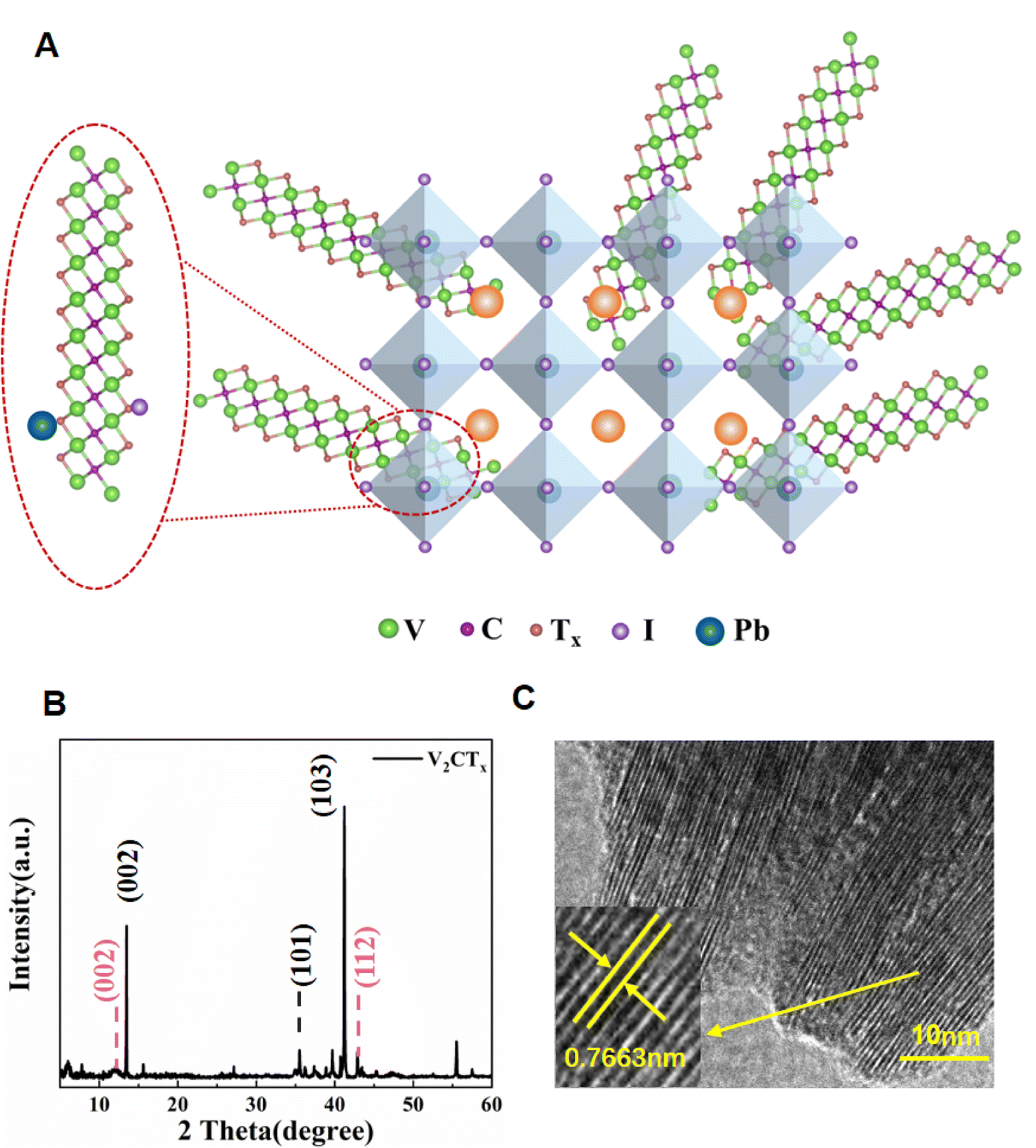 | ||
| Fig. 1 (A) Schematic illustration of the V2CTx MXene effect on the perovskite film. (B) XRD spectra of V2CTx MXene. (C) High-resolution TEM image of V2CTx MXene. | ||
To investigate the morphology change induced by V2CTx, top view SEM images of the perovskite film washed only with CB (control) are shown in Fig. 2A and S5A,† and those for the V2CTx-washed (0.01 mg mL−1) perovskite film (target) are shown in Fig. 2B and S5B,† respectively. All the perovskite film surfaces are quite smooth, which is consistent with previous studies indicating that employing CB anti-solvent is an efficient method to improve the perovskite film quality.28Fig. 2C shows an average grain size of ∼600 nm for the target perovskite film which is obviously larger than that (∼450 nm) of the control sample. The atomic force microscopy (AFM) images of the reference and target perovskite films are shown in Fig. 2D and E, and height analysis in Fig. 2F, respectively. The root mean square roughness (RMS) of the target perovskite film is 17.7 nm, which is smaller than 25.6 nm for the control perovskite film. The reduced roughness of the target perovskite film is believed to be beneficial to avoid shunt and defect in the perovskite/HTL interface. The more conducive interface additive will facilitate hole injections from the perovskite to the HTL. Fig. S6A and B† show the cross-sectional SEM images of perovskite/SnO2 interfaces. Compared with the obvious GBs and cracks in the control perovskite layer, the target film layer becomes dense after treatment, and the GBs and cracks are significantly reduced.
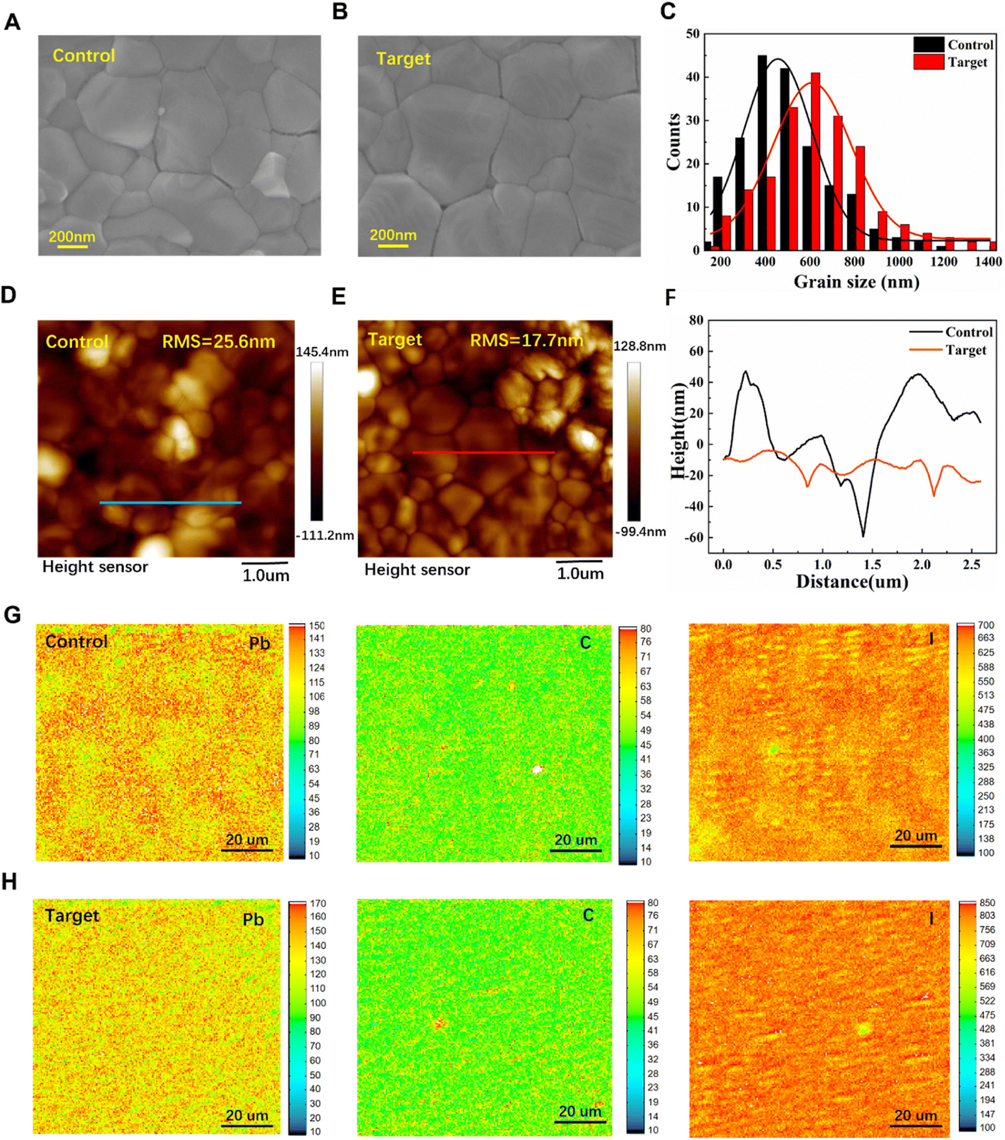 | ||
| Fig. 2 (A) and (B) Top view SEM images of the (A) control perovskite film (0 mg mL−1 V2CTx) and (B) target perovskite film (0.01 mg mL−1 V2CTx). (C) Statistical distribution of the grain sizes for control and target perovskite films on a SnO2 substrate. (D)–(E) AFM images of the control perovskite film and target perovskite film. (F) Height analysis of the line in the two AFM images. (G) and (H) EPMA elemental mapping for Pb, I and C, scanning kelvin probe microscopy image for the control and target films on SnO2 substrates, respectively. | ||
The distribution of Pb, I and C in the two perovskite films can be analyzed by electron probe microanalysis (EPMA). As shown in Fig. 2G and H, there are obvious differences between the control and target films, with Pb and I being the most obvious cases. In the target film, the distribution of the three elements is very uniform. In Fig. 2G, it can be seen that Pb and I are randomly distributed in different places on the control film, and this phenomenon is also observed in C element, but its segregation is less severe. A C-rich region was found in the target film, and a small amount of V2CTx was presumed to be distributed in this region. In addition, we also analyzed the distribution of V and F elements in the target film shown in Fig. S7A and B.† The distribution of V2CTx on the target film is very small and uniform. In fact, this result is also consistent with the XPS and SEM analysis. In conclusion, the V2CTx additive can effectively improve the chemical uniformity of I, Pb and C in the film.
Fig. 3A illustrates the fabrication process of the perovskite Cs0.042FA0.763MA0.195Pb(I0.928Br0.056Cl0.016)3 films via an antisolvent assisted one-step deposition with anti-solvent washing and annealing treatments. The blue box shows the spin-coating stage and the anti-solvent dropping stage, and the red box represents the annealing stage of the film. In order to further study the nucleation and crystallization process of the perovskite, the spin coating stage and annealing stage of perovskite films were studied by in situ GIWAXS experiments, respectively. In this work, the V2C additive was introduced into CB anti-solvent for the first time, and then dropped onto the perovskite films during spin-coating. Fig. 3B–E show the 2D-GIWAXS patterns and the corresponding integrated curves of the control and target perovskite films collected from the spin-coating stage and anti-solvent dropping stage, respectively, which could visually illustrate the structural evolution in the process from the perovskite precursor solution to the as-deposited film. During the first ∼10 s, there are no obvious diffraction peaks in both samples, indicating that the amorphous phase occurred in the first stage of the spin-coating process; beginning at ∼20 s, several slight peaks located at q < 10 nm−1 gradually increased before dropping the anti-solvent, which implied the existence of a small amount of precursor phases in wet films; after dropping the CB anti-solvent, both samples show obvious peaks located at q ∼ 8.6 nm−1 and q ∼ 9.1 nm−1, assigned to the intermediate phase of perovskite and PbI2 phase, which is well consistent with the previous report.11 The yellow δ-phase of the perovskite in the target film demonstrated a higher intensity and a narrower peak width compared with those of the control film, indicating the higher crystallinity of the δ-phase perovskite induced by the V2CTx MXene additive in CB. Compared with the control film, it is notable that a series of diffraction spots appeared after the anti-solvent spin-coating stage (from 25 to 40 s), indicating the appearance of a low-dimensional perovskite structure (n < 3), which might contribute to improving the structural stability of the final film and devices. In addition, further in situ GIWAXS measurements for the annealing stage of these two perovskite films are summarized in Fig. S8,† which visually reveal the structural evolution of intermediate perovskite phases, including the low-dimensional perovskite structures, converting from the yellow phase to the final black phase.
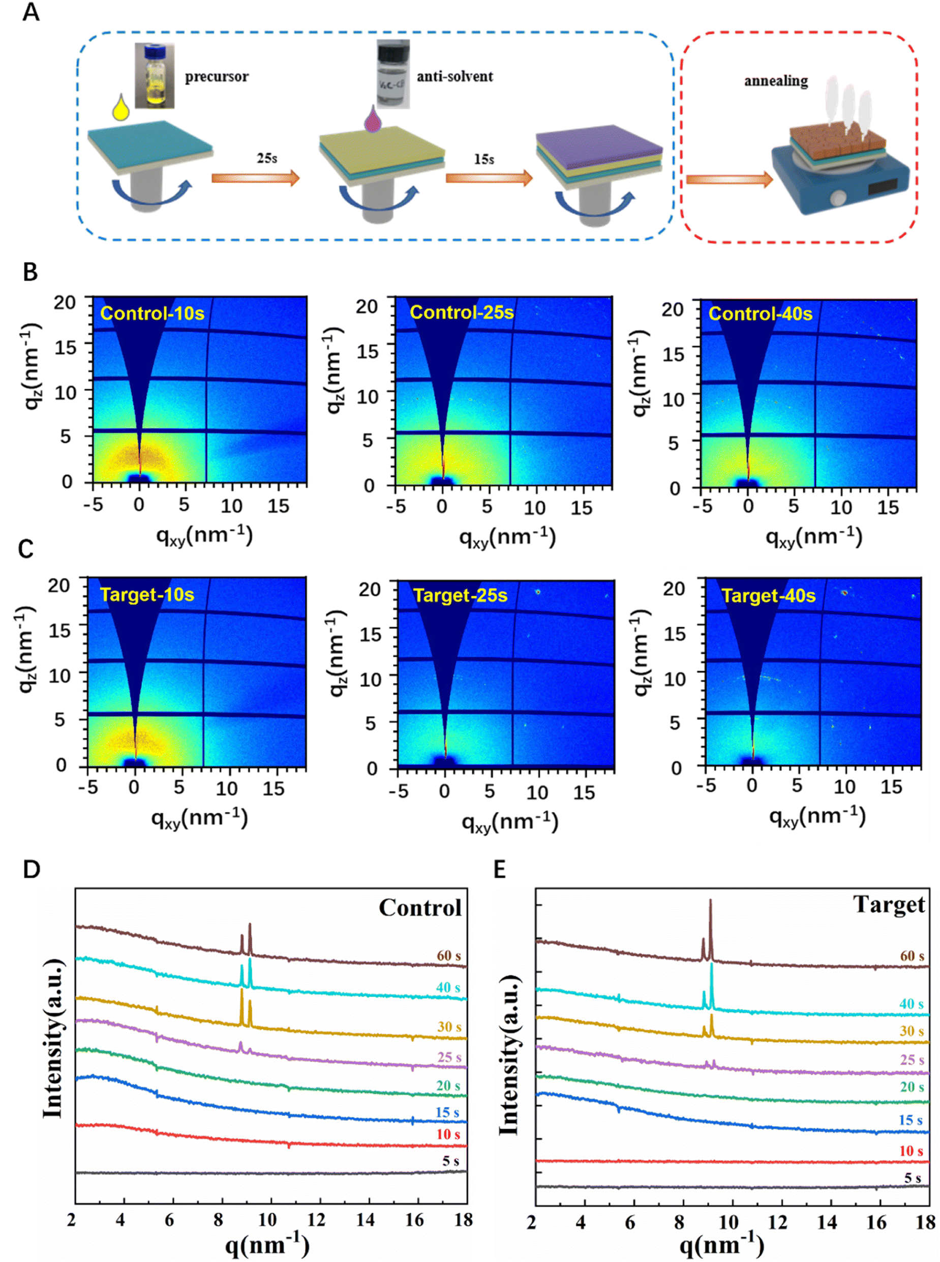 | ||
| Fig. 3 (A) The fabrication process of the Cs0.042FA0.763MA0.195PbI0.928Br0.056Cl0.016 film. (B) and (C) 2D-GIWAXS patterns and (D) and (E) the corresponding integrated curves of the control and target perovskite films collected from the spin-coating stage and anti-solvent dropping stage, respectively. | ||
Orientation and crystallization of the sintered perovskite films are characterized by 2D-GIWAXS as shown in Fig. 4A and B. The crystallographic structures of the control perovskite film and target perovskite film deposited on SnO2 substrates are collected at X-ray incident angles of 0.2° (surface) and 0.4° (bulk). All images have similar diffraction rings and spotty patterns, indicating that both films have high crystallinity and similar in-plane and out-of-plane orientations. Both perovskite films show typical diffraction rings at q ≈ 10, 20, 22.2 nm−1, where q is the scattering vector, corresponding to (110), (220) and (310) crystal planes. Obviously, it can be noted that the intensity of the diffraction rings of (110) and (220) planes increased both on the target-0.2 and target-0.4 perovskite film. In addition, the peak of PbI2 (001) at q ≈ 9 nm−1 is not observed in all 2D-GIWAXS images. To obtain specific information about the crystallinity, the high-resolution X-ray diffraction integral diagram (shown in Fig. 4C) and the radially integrated intensity plot along the (110) ring at q ≈ 10 nm−1 derived from 2D-GIWAXS patterns collected at two different incidence angles for both the control and target perovskite films, respectively, were obtained. It shows that the (110) diffraction peak from the target perovskite film is higher than that from the control perovskite film indicating that the V2CTx additive improves the degree of crystallinity of perovskite films, which is in agreement with the results observed by SEM. Meanwhile, it is noticed that all the (110) diffraction peaks show an asymmetrical intensity distribution comprised of two or three overlapping components, indicating that there were complex phases in the thin films. In addition, Fig. 4C shows that the control-0.2 film and control-0.4 film have small wide peaks at q ≈ 9 nm−1, which correspond to the residue of PbI2 on the surface and bulk of the control perovskite film. The presence of PbI2 implies that the perovskite film might begin to degrade, indicating the lower structural stability of the control film compared with the target perovskite film with V2CTx passivation.
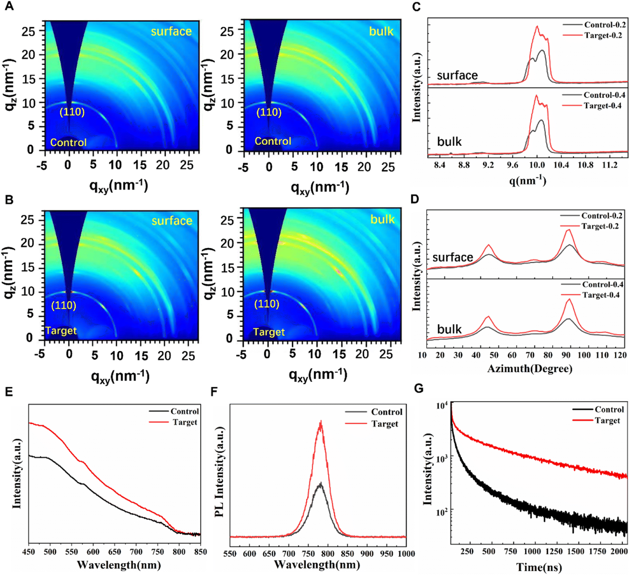 | ||
| Fig. 4 2D-GIWAXS images of the control perovskite film and V2C-washed target perovskite film deposited on SnO2 substrates (incident angle of (A) 0.2° and (B) 0.4°), respectively. (C) High-resolution X-ray diffraction integral diagram of the two perovskite films (incident angle of 0.2° and 0.4°). (D) Radially integrated intensity plots along the ring at q = 10 nm−1, assigned to the (110) plane of the two perovskite films (incident angle of 0.2° and 0.4°). (E) Ultraviolet-visible (UV-vis) absorption spectra, (F) PL spectra and (G) time-resolved PL spectrum of the control perovskite film and target perovskite film deposited on glass substrates. | ||
We also noticed that the small peak at q ≈ 8.6 nm−1 in the control-0.4 film corresponded to the presence of the yellow δ-phase in the bulk of the thin film, which was not completely transformed into the black α-phase. The radially integrated intensities of different 2D-GIWAXS patterns along the ring at q = 10 nm−1 plotted as a function of azimuth angle are exhibited in Fig. 4D, which are assigned to the (110) plane of the perovskite film. The intensity of the sharp and narrow peaks at the azimuth angle of 90° and 42.5° both increased, suggesting the preferential orientation of the perovskite after V2CTx addition.19,29 In addition, additional weak peaks at the azimuth angles of 70° (180°–70°) were observed for the target perovskite film. This demonstrates the multiple preferential orientation of the perovskite film after V2CTx addition, which achieved efficient charge transport along multiple directions within the perovskite active layer.30
Fig. 4E shows the UV-vis absorption spectra of the reference and target perovskite films deposited on the glass substrates. The two perovskite films showed similar absorption edges, suggesting that the band gap (∼1.54 eV) of the perovskite remained unchanged after the addition of V2CTx shown in Fig. S9.† Compared with the control perovskite film, an obvious higher absorbance is observed in the 400–750 nm region for the target perovskite film, indicating the better film quality of the perovskite deposited with the V2CTx MXene dopant.
As shown in Fig. 4F, the steady-state photoluminescence (PL) intensity of the target perovskite film was significantly stronger compared with the control perovskite film, indicating that nonradiative recombination in the target perovskite film is suppressed.
Time-resolved photoluminescence (TRPL) spectra were measured to evaluate the carrier's lifetime for perovskites with and without V2CTx MXene on glass substrates (Fig. 4G). The TRPL spectra can be well fitted by the biexponential function below:31
Y = A1![[thin space (1/6-em)]](https://www.rsc.org/images/entities/char_2009.gif) exp(−t/τ1) + A2exp(−t/τ2) + y0 exp(−t/τ1) + A2exp(−t/τ2) + y0 | (1) |
The XPS of I 3d and Pb 4f collected for both the reference and target perovskite films are shown in Fig. 5A and B respectively. The I 3d spectrum of the target perovskite film shifted towards the high binding energy compared with that of the reference film, suggesting the chemical interaction between V2CTx and perovskite. Compared with the control perovskite film, the Pb 4f spectra of the target perovskite film showed a slight shift to the higher binding energy side. As previously reported, the Pb2+ peaks were assigned at ≈143.3 eV (4f5/2) and ≈138.4 eV (4f7/2), and two shoulder peaks assigned at ≈141.6 eV (4f5/2) and ≈136.8 eV (4f7/2) were from the Pb0 metal,33–35 respectively. In addition, no obvious peaks of metallic Pb0 were observed in the target perovskite film, indicating that the Pb2+ on the surface of the perovskite film has been effectively stabilized by the addition of V2CTx.34,35 The metallic Pb defects also indicate the existence of iodide vacancies in the control perovskite lattice and act as nonradiative recombination centers, hindering carrier transfer and collection.36 The results prove that the defects in the perovskite film were significantly suppressed due to the Tx treatment and the PL life time increased, which is consistent with the results of TRPL spectra. The C 1s and O 1s spectra are shown in Fig. S10A–C.† For the C 1s spectra of the target film, a new peak appeared at 282.58 eV attributed to C–V bands in V2CTx. The O 1s spectrum of the target film was taller and narrower than that of the control film, which demonstrated that V2CTx can interact with organic cations and inhibit ion migration. We can't find the V signal in XPS results, indicating that very little V2CTx was present on the surface of the film. To further verify the incorporation of V2CTx MXene and the surface of the thin perovskite film successfully, Fig. S10D† shows the soft X-ray absorption spectroscopy (sXAS) spectra of the control perovskite film and target perovskite film. Clearly, only the surface of the target perovskite film can detect the signal of vanadium. The overall spectra can be divided into two parts, the L3-edge at the energy range of 513–520 eV and the L2-edge at 520–528 eV, which originated from the 2p core hole spin–orbital splitting of vanadium as reported previously.37 Fig. S11† shows the IR spectra of the control film, target film and V2CTx. The two perovskite films did not show any obvious difference, which indicates that very little V2CTx remained in the perovskite.
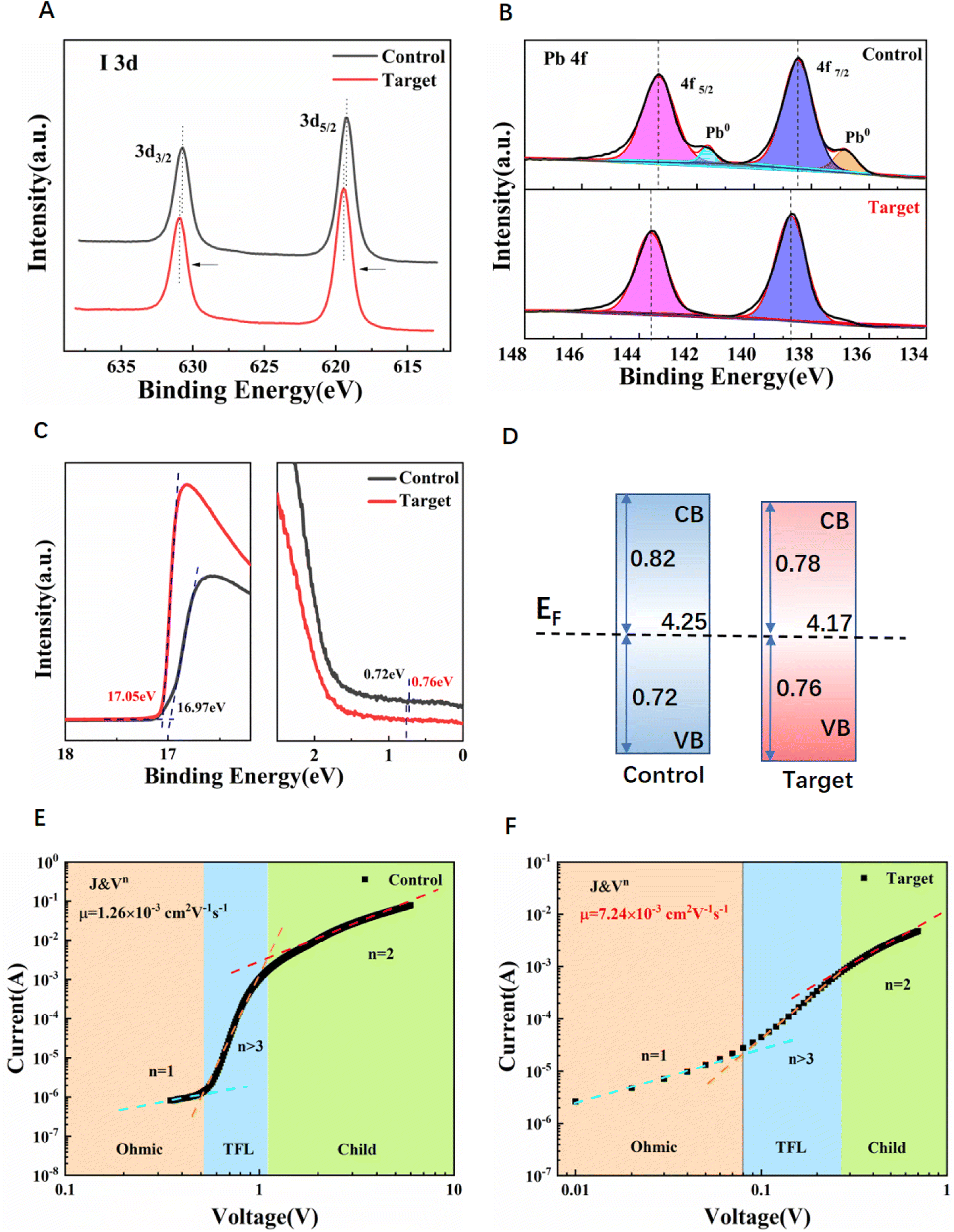 | ||
| Fig. 5 (A) and (B) XPS of I 3d and Pb 4f from control and target perovskite films on the SnO2 substrate. (C) UPS of control and target perovskite films on SnO2 substrates. Work function was calculated by subtracting 21.22 eV from the spectrum edge. (D) Energy level alignment of control and target perovskites. (E) and (F) Space charge limit current (SCLC) of control and target perovskite films. | ||
Fig. 5C shows the ultraviolet photoelectron spectroscopy (UPS) spectra of both the control and target perovskite films on SnO2 substrates. The work function (WF) is the energy difference between the vacuum level and the Fermi level. According to the secondary electron cutoff edge, the WF of the control and target films can be calculated as −4.25 eV and −4.17 eV, respectively. In the binding energy region, the distances between the valence-band maximum (VBM) and the Fermi level of the control film and the target film are 0.72 eV and 0.76 eV, respectively. Consequently, the VBM of the control film and target film was calculated to be −4.97 eV and −4.93 eV. Based on the Tauc plot (Fig. S9†), the conduction band minimum (CBM) is estimated to be around −3.43 eV and −3.39 eV for the control and target films, respectively. The energy level diagrams of the control film and the target film shown in Fig. 5D show that the band alignment between the perovskite and transport layer is improved after V2CTx passivation, which is more conducive to carrier extraction from the perovskite to the transport layer. Improved interface level matching is also a method for enhanced interface carrier extraction and performance improvement of the device.
For further study the electron mobility (μe) and trap density (ntrap) of perovskite films, and space charge limit current (SCLC) measurement with the structure of ITO/SnO2/Cs0.042FA0.763MA0.195PbI0.928Br0.056Cl0.016/PC61BM/BCP/Ag (electron-only device) are shown in Fig. 5E and F. ntrap can be obtained by this formula as follows:38
 | (2) |
μ e of the samples can be calculated as follows:39,40
 | (3) |
μ e of the target perovskite film is 7.24 × 10⁻³ cm2 V−1 s−1, which is four times higher than 1.76 × 10⁻³ cm2 V−1 s−1 for the control perovskite film. The increased electron mobility can be attributed to the reduction of defects of perovskite films, thus facilitating electron transport.
As shown in Fig. S12A and B,† the contact angles of spiro-OMeTAD on the control perovskite film and V2CTx-washed target perovskite film on SnO2 surfaces show a slight difference, indicating the similar affinity between the active perovskite layer and the hole transport layer.31
We fabricated the PSCs with a planar structure ITO/SnO2/perovskite/spiro-OMeTAD/Ag (Fig. 6A). The current density versus voltage (J–V) curves of the different concentrations of V2CTx doped devices are shown in Fig. 6B. When the concentration of V2CTx in the CB solution increased from 0 to 0.005, 0.01, 0.015 and 0.02 mg mL−1, the PCEs of PSCs also increased from 19.5% to 21.1%, 23.47%, and then decreased to 22%, 21%. Therefore, the V2CTx concentration of the champion PSC is determined to be 0.01 mg mL−1. Fig. 6C demonstrates the best J–V characteristics of the corresponding PSC devices based on the control perovskite film and target perovskite film. The control device exhibits a remarkable PCE of 20.1%, with a Voc of 1.144 V, short-circuit current density (Jsc) of 24.21 mA cm−2, and fill factor (FF) of 72.5%, while the target device delivers a significantly improved PCE of 23.47%, with Voc of 1.175 V, Jsc of 25.03 mA cm−2, and FF of 79.9%. We noticed that negligible hysteresis was found between the forward scan and reverse scan of the target device compared with the control device as shown in Fig. 6D, which may be related to the improvement of electron mobility and carrier lifetime. The detailed photovoltaic performance parameters of the control and target PSCs under both forward and reverse scans are shown in Table S2.† As shown in Fig. 6E, the integrated current densities of control and target devices calculated from the incident photon-to-electron conversion efficiency (IPCE) were 22.51 and 24.69 mA cm−2. The target device based on the V2CTx-modified perovskite film exhibited strong light-harvesting capability in the same spectral range. In addition, in order to further study the recombination of photogenerated carriers in the device, the Voc curves of two perovskite devices with different light intensities were tested (Fig. 6F). The ideality factor α was obtained according to the following formula (4):
 | (4) |
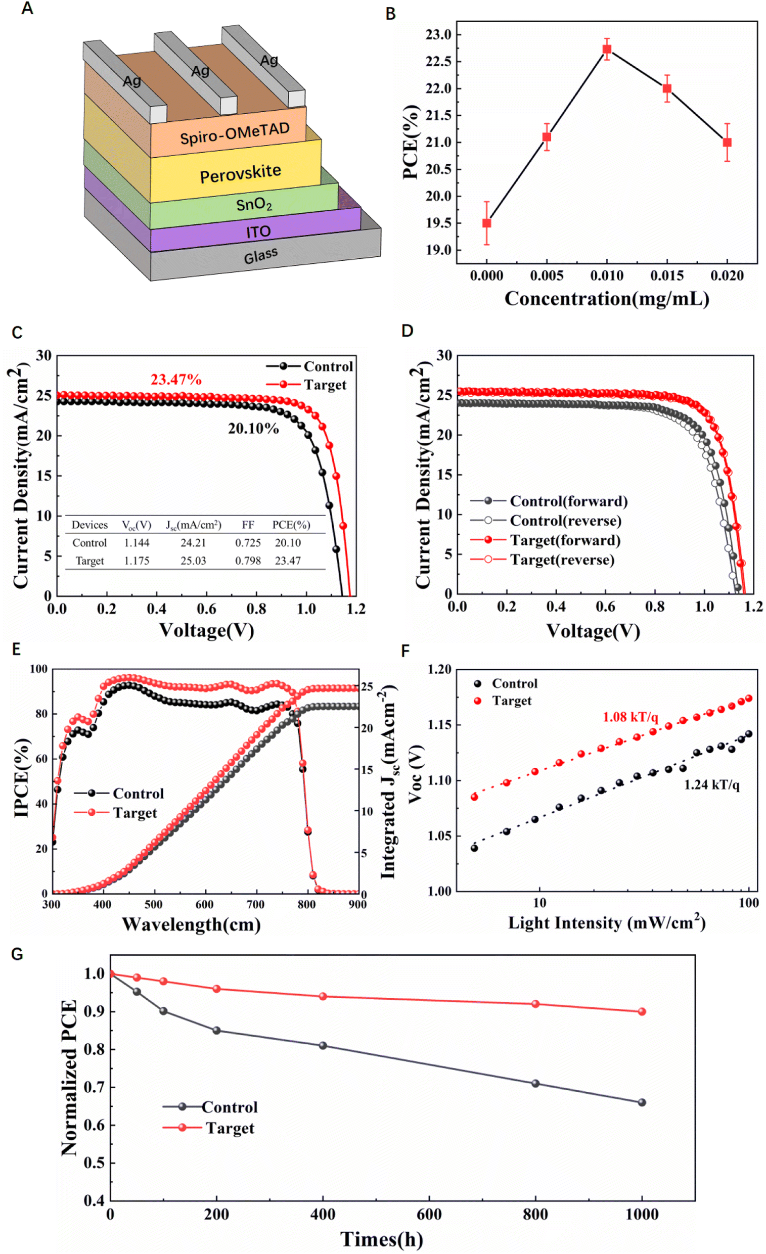 | ||
| Fig. 6 (A) Device structure of the perovskite solar cells. (B) J–V curves of the different concentrations of V2C doped devices. (C) J–V curves of the best-performing PSCs based on the control and target device. (D) The J–V curves of control and target devices under forward and reverse scans. (E) The IPCE curves and integrated Jsc of control and target devices. (F) Voc and the relevant fitting curves under different illuminated light intensities for the control and target devices. (G) The device stability of the control and target PSC exposure under 40–60% environmental humidity at room temperature in N2 for 1000 h. | ||
To further confirm that the addition of V2CTx improved the device performance, the device stability was monitored in the dark in N2 at room temperature under 40–60% environmental humidity as shown in Fig. 6G. The target device retains 90% of its original PCE after 1000 h exposure, while the control device only retains 75% of its original PCE after the same treatment. This significant improvement of the stability of PSC could be attributed to the decrease of GBs and high crystallinity of the perovskite film. As shown in Fig. S13,† in order to study the stability of modified perovskite films in air, the control and target films were placed on a heating plate in 60–70% ambient air at 100 °C for 0 h, 5 h, 24 h and 48 h to test the UV-vis absorption spectra and steady-state PL spectra of the two films, respectively. In Fig. S13A and B,† the target film still has good and stable absorption after 48 h compared with the control film. Interestingly, the PL intensity of both perovskite films increased and then decreased after heating as shown in Fig. S13C and D.† In addition, the PL mapping of the control and target films are shown in Fig. S14.† The target film had a stronger and more uniform fluorescence. After two hours of heating at 100 °C in air, the PL mapping images of the two perovskite films were all relatively enhanced, corresponding to the steady-state PL results. Furthermore, in situ GIWAXS measurements (Fig. S15A and C†) were performed on two perovskite films heated at 100 °C at a relative humidity of 50–70% in an ambient environment. Due to the relatively high humidity in the experimental environment, a small amount of PbI2 appeared in both perovskite films at the beginning of the measurement. During the heating process, the perovskite diffraction peak of the target film is more stable and decreases more slowly than the control film, which indicates that the V2CTx additive makes the perovskite film have better thermal stability.44 We also performed the GIWAXS experiments of the two perovskite films in an ambient environment with 30–50% humidity for 0 h and 14 h as shown in Fig. S15B and D.† The peak intensity of q = 10 nm−1 was weakened after the two perovskite films were placed for 14 h. A small amount of PbI2 was present in the control film, but no significant PbI2 was present in the target film. The above stability tests further prove that the addition of V2CTx MXene is an effective method to improve the efficiency and stability of PSCs.
Conclusion
In summary, we have introduced a novel CB anti-solvent with V2C MXene to prepare high-quality Cs0.042FA0.763MA0.195Pb(I0.928Br0.056Cl0.016)3-based PSCs with an increased PCE up to 23.47% from 20.1% of the control device. Notably, the V2C additive not only increased the grain size of the perovskite and reduced charge carrier recombination via GB passivation, but also reduced the Pb0 defect in the perovskite active layer and increased the charge carrier life and mobility, thus greatly improving the photovoltaic performance of PSCs. As a result, the control PSC had good device stability against humidity. This work provided a new insight for the crystallization modulation and surface passivation of perovskite films to improve the stability and PCE of PSCs, which is also conducive to the application of MXenes in PSCs.Conflicts of interest
The authors declare no conflicts of interest.Acknowledgements
We would like to thank Prof. Anders Hagfeldt for helping with the discussion, the accelerator scientists and the staff of beamlines BL17B1, BL14B1, BL11B1, BL19U2, BL15U and BL01B1 at SSRF for providing the beam time and User Experiment Assist System of SSRF for their help. We also thank the accelerator scientists and the staff of beamline 4B7B at BSRF for providing the beam time. We acknowledge the Photonics Science Center of CO2, National Key Research and Development Program of China (2017YFA0403400), the National Natural Science Foundation of China (Grant No. 12175298, 12075309, 11605278, 11705271, U1932119, U1632268, U1632121), the research grant (No. 17YF1423700) from the Shanghai Sailing Program, Shanghai Municipal Commission for Science and Technology (No. 20ZR1464100), Youth Innovation Promotion Association CAS (2021284), Shanghai Large Scientific Facilities Center, and Fudan University Talent Introduction Project. We also thank TILON Group Technology Limited (Division of China) for their help in the characterization.References
- Y. Yang, H. Lu, S. Feng, L. Yang, H. Dong, J. Wang, C. Tian, L. Li, H. Lu, Y. Liu, M. Gratzel and A. Hagfeldt, Energy Environ. Sci., 2021, 14, 3447 RSC.
- H. Lu, Y. Liu, P. Ahlawat, A. Mishra, W. R. Tress, F. T. Eickemeyer, Y. Yang, F. Fu, Z. Wang, C. E. Avalos, B. I. Carlsen, A. Agarwalla, X. Zhang, X. Li, Y. Zhan, S. M. Zakeeruddin, L. Emsley, U. Rothlisberger, L. Zheng, A. Hagfeldt and M. Gratzel, Science, 2020, 370, eabb8985 CrossRef CAS PubMed.
- J. Jeong, M. Kim, J. Seo, H. Lu, P. Ahlawat, A. Mishra, Y. Yang, M. A. Hope, F. T. Eickemeyer, M. Kim, Y. J. Yoon, I. W. Choi, B. P. Darwich, S. J. Choi, Y. Jo, J. H. Lee, B. Walker, S. M. Zakeeruddin, L. Emsley, U. Rothlisberger, A. Hagfeldt, D. S. Kim, M. Gratzel and J. Y. Kim, Nature, 2021, 592, 381 CrossRef CAS PubMed.
- J. Yang, C. Liu, C. Cai, X. Hu, Z. Huang, X. Duan, X. Meng, Z. Yuan, L. Tan and Y. Chen, Adv. Energy Mater., 2019, 9, 1900198 CrossRef.
- N R E Laboratory, https://www.nrel.gov/pv/cell-efficiency.html, accessed February 2022.
- N. Li, S. Tao, Y. Chen, X. Niu, C. K. Onwudinanti, C. Hu, Z. Qiu, Z. Xu, G. Zheng, L. Wang, Y. Zhang, L. Li, H. Liu, Y. Lun, J. Hong, X. Wang, Y. Liu, H. Xie, Y. Gao, Y. Bai, S. Yang, G. Brocks, Q. Chen and H. Zhou, Nat. Energy, 2019, 4, 408 CrossRef CAS.
- D. Z. Chen, H. Dong, S. Z. Pang, W. D. Zhu, H. Xi, Z. H. Lin, J. J. Chang, J. C. Zhang, C. F. Zhang and Y. Hao, Org. Electron., 2019, 70, 300 CrossRef CAS.
- H. Lu, A. Krishna, S. M. Zakeeruddin, M. Gratzel and A. Hagfeldt, iScience, 2020, 23, 101359 CrossRef CAS PubMed.
- Y. Wu, X. Yang, W. Chen, Y. Yue, M. Cai, F. Xie, E. Bi, A. Islam and L. Han, Nat. Energy, 2016, 1, 16148 CrossRef CAS.
- M. Jeong, I. W. Choi, E. M. Go, Y. Cho, M. Kim, B. Lee, S. Jeong, Y. Jo, H. W. Choi, J. Lee, J.-H. Bae, S. K. Kwak, D. S. Kim and C. Yang, Science, 2020, 369, 1615 CrossRef CAS PubMed.
- K. Zhang, Z. Wang, G. Wang, J. Wang, Y. Li, W. Qian, S. Zheng, S. Xiao and S. Yang, Nat. Commun., 2020, 11, 1–11 CrossRef PubMed.
- N. J. Jeon, J. H. Noh, Y. C. Kim, W. S. Yang, S. Ryu and S. Seok, Nat. Mater., 2014, 13, 897 CrossRef CAS PubMed.
- W. Li, M. U. Rothmann, Y. Zhu, W. Chen, C. Yang, Y. Yuan, Y. Y. Choo, X. Wen, Y.-B. Cheng, U. Bach and J. Etheridge, Nat. Energy, 2021, 6, 624 CrossRef CAS.
- K. Wang, Y. Yang, Y. Lou, M. Li, F. Igbari, J. Cao, J. Chen, W. Yang, C. Dong, L. Li, R. Tai and Z. Wang, eScience, 2021, 1, 53 CrossRef.
- C. Liu, Z. Huang, X. Hu, X. Meng, L. Huang, J. Xiong, L. Tan and Y. Chen, ACS Appl. Mater. Interfaces, 2018, 10, 1909 CrossRef CAS PubMed.
- L. Li, Y. Chen, Z. Liu, Q. Chen, X. Wang and H. Zhou, Adv. Mater., 2016, 28, 9862 CrossRef CAS PubMed.
- D. Bi, C. Yi, J. Luo, D. Décoppet, F. Zhang, S. M. Zakeeruddin, X. Li, A. Hagfeldt and M. Grätzel, Nat. Energy, 2016, 1, 16142 CrossRef CAS.
- Y. Gao, Y. Wu, H. Lu, C. Chen, Y. Liu, X. Bai, L. Yang, W. Yu, Q. Dai and Y. Zhang, Nano Energy, 2019, 59, 517 CrossRef CAS.
- Y. Yang, S. Feng, M. Li, F. Li, C. Zhang, Y. Han, L. Li, J. Yuan, L. Cao, Z. Wang, B. Sun and X. Gao, Nano Energy, 2018, 48, 10 CrossRef CAS.
- W. Xu, Y. Gao, W. Ming, F. He, J. Li, X.-H. Zhu, F. Kang, J. Li and G. Wei, Adv. Mater., 2020, 32, 2003965 CrossRef CAS PubMed.
- X. Li, C. Wang, Y. Cao and G. Wang, Chem.–Asian J., 2018, 13, 2742 CrossRef CAS PubMed.
- X. Zhang, J. Lei, D. Wu, X. Zhao, Y. Jing and Z. Zhou, J. Mater. Chem. A, 2016, 4, 4871 RSC.
- O. Mashtalir, M. Naguib, V. N. Mochalin, Y. Dall'Agnese, M. Heon, M. W. Barsoum and Y. Gogotsi, Nat. Commun., 2013, 4, 1716 CrossRef PubMed.
- Q. Hu, D. Sun, Q. Wu, H. Wang, L. Wang, B. Liu, A. Zhou and J. He, J. Phys. Chem. A, 2013, 117, 14253 CrossRef CAS PubMed.
- L. Huang, X. Zhou, R. Xue, P. Xu, S. Wang, C. Xu, W. Zeng, Y. Xiong, H. Sang and D. Liang, Nano-Micro Lett., 2020, 12, 44 CrossRef CAS PubMed.
- A. Agresti, A. Pazniak, S. Pescetelli, A. Di Vito, D. Rossi, A. Pecchia, M. A. D. Maur, A. Liedl, R. Larciprete, D. V. Kuznetsov, D. Saranin and A. Di Carlo, Nat. Mater., 2019, 18, 1264 CrossRef CAS PubMed.
- M. Naguib, J. Halim, J. Lu, K. M. Cook, L. Hultman, Y. Gogotsi and M. W. Barsoum, J. Am. Chem. Soc., 2013, 135, 15966 CrossRef CAS PubMed.
- M. Xiao, F. Huang, W. Huang, Y. Dkhissi, Y. Zhu, J. Etheridge, A. Gray-Weale, U. Bach, Y.-B. Cheng and L. Spiccia, Angew. Chem., Int. Ed., 2014, 53, 9898 CrossRef CAS PubMed.
- S. Feng, Y. Yang, M. Li, J. Wang, Z. Cheng, J. Li, G. Ji, G. Yin, F. Song, Z. Wang, J. Li and X. Gao, ACS Appl. Mater. Interfaces, 2016, 8, 14503 CrossRef CAS PubMed.
- S. Wang, P. Wang, B. Chen, R. Li, L. Ren, Y. Li, B. Shi, Q. Huang, Y. Zhao, M. Grätzel and X. Zhang, eScience, 2022, 2, 339 CrossRef.
- J. Yang, C. Liu, C. Cai, X. Hu, Z. Huang, X. Duan, X. Meng, Z. Yuan, L. Tan and Y. Chen, Adv. Energy Mater., 2019, 9, 1900198 CrossRef.
- F. Ye, J. Ma, C. Chen, H. Wang, Y. Xu, S. Zhang, T. Wang, C. Tao and G. Fang, Adv. Mater., 2021, 33, 2007126 CrossRef CAS PubMed.
- N. Chen, X. Yi, J. Zhuang, Y. Wei, Y. Zhang, F. Wang, S. Cao, C. Li and J. Wang, Nano-Micro Lett., 2020, 12, 177 CrossRef CAS PubMed.
- S. Song, E. Y. Park, B. S. Ma, D. J. Kim, H. H. Park, Y. Y. Kim, S. S. Shin, N. J. Jeon, T.-S. Kim and J. Seo, Adv. Energy Mater., 2021, 11, 2003382 CrossRef CAS.
- F. Li, X. Deng, F. Qi, Z. Li, D. Liu, D. Shen, M. Qin, S. Wu, F. Lin, S.-H. Jang, J. Zhang, X. Lu, D. Lei, C.-S. Lee, Z. Zhu and A. K. Y. Jen, J. Am. Chem. Soc., 2020, 142, 20134 CrossRef CAS PubMed.
- D. Bi, C. Yi, J. Luo, J.-D. Decoppet, F. Zhang, S. M. Zakeeruddin, X. Li, A. Hagfeldt and M. Grätzel, Nat. Energy, 2016, 1, 16142 CrossRef CAS.
- S.-M. Bak, R. Qiao, W. Yang, S. Lee, X. Yu, B. Anasori, H. Lee, Y. Gogotsi and X.-Q. Yang, Adv. Energy Mater., 2017, 7, 1700959 CrossRef.
- T. Niu, J. Lu, M.-C. Tang, D. Barrit, D.-M. Smilgies, Z. Yang, J. Li, Y. Fan, T. Luo and I. McCulloch, Energy Environ. Sci., 2018, 11, 3358 RSC.
- H. Zhu, Z. Shen, L. Pan, J. Han, F. T. Eickemeyer, Y. Ren, X. Li, S. Wang, H. Liu, X. Dong, S. M. Zakeeruddin, A. Hagfeldt, Y. Liu and M. Grätzel, ACS Energy Lett., 2021, 6, 208 CrossRef CAS.
- Q. F. Han, S. H. Bae, P. Y. Sun, Y. T. Hsieh, Y. Yang, Y. S. Rim, H. X. Zhao, Q. Chen, W. Z. Shi and G. Li, Adv. Mater., 2016, 28, 2253 CrossRef CAS PubMed.
- X. Du, O. Lytken, M. S. Killian, J. Cao, T. Stubhan, M. Turbiez, P. Schmuki, H. Steinrück, L. Ding, R. H. Fink, N. Li and C. J. Brabec, Adv. Energy Mater., 2017, 7, 1601959 CrossRef.
- T. Singh, S. Öz, A. Sasinska, R. Frohnhoven, S. Mathur and T. Miyasaka, Adv. Funct. Mater., 2018, 28, 1706287 CrossRef.
- D. B. Khadka, Y. Shirai, M. Yanagida, J. W. Ryan and K. Miyano, J. Mater. Chem. C, 2017, 5, 8819 RSC.
- S. Yu, J. Meng, Q. Pan, Q. Zhao, T. Pullerits, Y. Yang, K. Zheng and Z. Liang, Energy Environ. Sci., 2022, 15, 3321 RSC.
Footnotes |
| † Electronic supplementary information (ESI) available. See DOI: https://doi.org/10.1039/d2ta05836g |
| ‡ These authors (Chen Tian, Yajie Yan and Shanglei Feng) contributed equally to this paper. |
| This journal is © The Royal Society of Chemistry 2023 |