Electrodeposited CuSbTe thin films with enhanced thermoelectric performance†
Received
27th April 2023
, Accepted 16th July 2023
First published on 17th July 2023
Abstract
Antimony telluride (Sb2Te3) based alloys are well known as promising thermoelectric materials for near-room temperature applications. In this work, we present a simple and cost effective electrodeposition approach for developing CuSbTe films with enhanced thermoelectric characteristics. Amorphous CuSbTe solid solutions of varied compositions are electrodeposited by adjusting the [Cu2+] concentration in the electrolytes. The increasing copper content in the films resulted in a crystalline to amorphous phase transition. This Cu-induced phase transition creates anti-site defects, resulting in lower carrier concentration, increased Hall mobility, and a higher Seebeck coefficient. The CuSbTe film with 5.7 at% Cu has an extraordinarily high power factor of 2.8 mW m−1 K−2, which originates from a high Seebeck coefficient of −382 μV K−1 and a good electrical conductivity of 2.05 × 10⁴ S m−1. To demonstrate the feasibility of applying this material as an n-type leg, the film is electrodeposited onto flexible Nylon cloth and validated for device fabrication. By delivering a maximum power output of 120 nW for a temperature difference of 30 K, our flexible device confirmed the prospective of this material in flexible thermoelectric device applications.
1. Introduction
The dramatic rise in energy consumption, combined with climate change caused by the extensive use of traditional fossil fuels, has motivated a quest for environmentally acceptable and renewable energy sources. Thermoelectric (TE) energy conversion is a potentially sustainable energy source and a viable method to achieve global carbon neutrality because of its ability to transform waste heat into power. The thermoelectric energy conversion efficiency is determined by a material's dimension-less figure of merit, zT = S2σk−1T,1 where σ, S, k and T are the electrical conductivity, Seebeck coefficient, thermal conductivity and absolute temperature, respectively.2 To maximize the thermoelectric efficiency, it is necessary to increase the power factor, S2σ while decreasing the thermal conductivity, k. However, these σ, S, and k are all inter-related and therefore, increasing the energy efficiency presents considerable challenges. To address this inherent disadvantage, many researchers attempted to tune these parameters via quantum confinement, phonon scattering, and energy filtering effects.3 To date, two different approaches have been followed to improve the thermoelectric performance of a material, such as introducing complex lattice structures and incorporating metallic or semiconducting nanoparticles into thermoelectric matrices.4,5 This work investigates a more traditional strategy for optimizing the thermoelectric performance by tuning the electron configuration or varying the carrier density near the Fermi-level through the doping process as reported earlier.3 The anomalies in the density of states cause a drastic rise in the Seebeck coefficient without lowering electrical conductivity, thus increasing the power factor.3
Thin films of antimony telluride (Sb2Te3) are one of the well-established thermoelectric materials for room temperature applications, because of their viable thermoelectric characteristics.56 This telluride has been extensively investigated and numerous groups have demonstrated that a marginal change in the chemical composition by doping Na,7 Bi,8 Ag,9 Cu10 and Sn11 can greatly improve its thermoelectric performance. Copper-doped multinary thermoelectric materials are gaining prominence due to their outstanding electronic transport characteristics and low inherent thermal conductivity.12 To obtain low dimensional films with these elements by conventional methods such as sputtering, thermal evaporation, and epitaxial growth is still challenging and of interest due to their phase transformation during the growth process.13,14 As a result, high-quality Sb2Te3 thin films prepared via a more traditional deposition approach are required for practical applications. Various methods have been used for the fabrication of thermoelectric materials with different elemental doping methods, such as solvothermal synthesis,15 chemical vapour deposition (CVD),16 atomic layer deposition (ALD),17 hydrothermal processes18 and electrodeposition methods.19 Electrodeposition is a highly productive and adaptable method that offers high deposition rates, scalability, ease of operation, low cost, and precise control over a variety of parameters such as composition and morphology.6 Padmanathan et al. reported that increasing the Cu content in electrodeposited CuBiTe20 or even in the Te film21 improved the power factor. The Cu-doping reduced the carrier concentration, leading to a larger Seebeck coefficient at room temperature. In 2021, Kim et al.22 reported controlled doping of Cu in n-type BiTeSe, observing that doped Cu generates one electron and acts as an electron connector, increasing the zT by 30% in the temperature range of 360–400 K. It is also reported that Cu doping in Ba8Ga16Sn30 enhanced its thermoelectric performance and showed a zT of 1.45 at around 500 K,23. Li et al.24 reported the effects of Cu2+ in the BiSbTe thin film and demonstrated an increase in the Seebeck coefficient. Park et al.25 investigated the thermoelectric properties of the intermetallic copper telluride thin film, and the band offset between the copper telluride and Te metal increases the Seebeck coefficient without sacrificing the film's conductivity due to carrier filtering. These aforementioned chemical strategies are well established and have been effectively utilized for various forms of chalcogenides, all of which show promise for applications in thermoelectric power generation. Another potentially effective technique for increasing the power factor is to modify the materials' intrinsic defects. This concept has been utilized extensively for IV–VI compounds (i.e. PbTe, SnTe, etc.) when alloying with I–V–VI2 (CuSbTe2, NaSbTe2) and has achieved excellent thermoelectric performance.26,27 The same approach has been adopted for V–VI compounds (i.e. Bi2Te3) when alloying with group I (Cu) elements and thus greatly enhanced the power factor because of disordered crystal structure. Surprisingly, the co-deposition of Cu with chalcogenides destroys the base crystal structure and the film becomes amorphous.20,28 This may be due to the transformation of the Bi2Te3 crystalline phase to the amorphous CuBiTe alloy during Cu co-deposition.29 This crystalline-to-amorphous transition increases the number of defects, including anion/cation (Bi/Te) vacancies, anti-site defects, grain boundaries, dislocations, etc., and strongly influences the carrier concentration, electrical conductivity and mobility.29 As a result of increased vacancy concentration, the power factor is greatly enhanced.20 However, the mechanism involved in Cu co-deposition and the formation of an amorphous ternary alloy is not clear yet. In addition, it is very challenging to investigate their intrinsic thermoelectric characteristics along with the base crystallite structure. Thus, more research is required to understand the effect of Cu on the formation of an amorphous electrodeposit during co-deposition.
To understand the effect of the amorphous CuSbTe alloy on the defect chemistry and thermoelectric properties of Sb2Te3, we performed a detailed study of co-deposited CuSbTe by varying Cu-concentrations. The as-deposited thin films are characterized using a combination of spectro-analytical techniques. The structural characterisation demonstrates that the films become completely amorphous after Cu addition while the underlying base crystalline structure persists. The formation of amorphous CuSbTe increases the Te vacancies, which in turn increases the electron charge carrier. Room temperature Hall measurements explain the effect of amorphous CuSbTe embedded with Sb2Te3 nanocrystallites, revealing low carrier concentration and good mobility for films deposited from a 0.4 mM Cu concentration bath. Thermoelectric transport property measurements reveal that the as-deposited films containing 5.7 atomic % Cu have a high Seebeck coefficient (−382 μV K−1) and outstanding power factor of 2.8 mW m−1 K−2 at room temperature. This investigation emphasizes the significance of intrinsic defects, such as atomic vacancies, grain boundaries in disordered crystal structure and their influence on thermoelectric performance. The film produced on a flexible Nylon substrate further validates the material's practical applicability in power generation.
2. Experimental
2.1 Fabrication of thin films
The electrolyte solutions for Sb2Te3 and ternary CuSbTe electrodeposition are prepared by using Sb2O3 (Sigma-Aldrich, 99.99%), TeO2 (Sigma-Aldrich, 99.995%), CuSO4·5H2O (Fisher Scientific, ≥99.0%), tartaric acid (ACS reagent ≥99.5%) and HNO3 (Sigma-Aldrich, ≥70%). For the binary Sb2Te3 electrolyte, two separate solutions are prepared in order to dissolve the salts. First, 2.4 mM Sb2O3 is dissolved in a 50 mM tartaric acid solution at 60 °C and then 3.6 mM TeO2 in 1 M HNO3. Then both prepared solutions are mixed together and DI water is added to reach the final 200 ml solution. The same procedure is followed to prepare the CuSbTe electrolyte solution by adding different concentrations of CuSO4·5H2O (0, 0.2, 0.4, 0.6, 0.8, 1.0 mM) in the above mixed solution. To determine the co-deposition potential, cyclic voltammetry is used using a CHI660C potentiostat in a three-electrode configuration with Ag/AgCl as the reference electrode, a standard gold electrode as the working electrode, and a platinized titanium mesh as a counter electrode. The Sb2Te3 and ternary CuSbTe films are electrodeposited onto a 20/10 nm Au/Ti coated Si/SiO2 substrate with an area of 32 × 32 mm2 in a three-electrode configuration. The deposition is carried out for 5 hours (h) at a constant potential of −150 mV. Following deposition, all the films are rinsed with DI water and dried with a nitrogen (N2) jet.
2.2 Thin film characterisation
The sample thickness is measured with a Dektak surface profilometer, within a ±0.1 μm tolerance. A scanning electron microscope (SEM Quanta FEG 450) with an attached energy-dispersive spectrometer (EDX) (Oxford laboratory EDX) is used to examine the morphology and composition of the deposited samples. The X-ray diffraction (XRD) patterns of the films are recorded using a Philips PW3710-MPD diffractometer using the Cu Kα radiation (λ = 1.54 Å). The Raman spectra are captured using a Renishaw (RA100) inVia confocal Raman microscope at 514.5 nm excitation. X-ray photoelectron spectroscopy (XPS) is carried out on a Kratos Ultra DLD spectrometer using the Al Kα source (1486.6 eV). The lamella is prepared in an FIB STEM [TESCAN SOLARIS] and examined by high-angle annular dark field scanning TEM (TITAN THEMIS S/TEM) and high resolution transmission electron microscopy (JEOL 2100FE HRTEM at 200 kV).
The Seebeck coefficient is measured using a custom-made Seebeck measurement system, where all the measurements are performed in the in-plane orientation.21 The temperature gradient is established along the two ends of a 5 × 32 mm2 long strip for the Seebeck measurement. The Seebeck coefficient is determined from the slope of the plotted thermo-voltage as a function of the temperature gradient in increments of 2 °C across the sample (S = ΔV/ΔT). The electrical conductivity, Hall mobility and carrier concentration of the films are measured using the van der Pauw geometry with four-point probes on a 1 cm2 sample using the LakeShore fully integrated system (LakeShore 8400) in a magnetic field of 1.7 T.
3. Results and discussion
3.1 Electrochemical co-deposition of CuSbTe
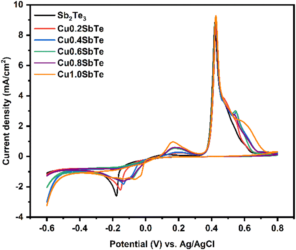
The cyclic voltammetry (CV) of Sb2Te3 and CuSbTe solutions is performed to investigate the oxidation–reduction potential for the electrodeposition process. A standard Au working electrode with a radius of 1 mm is employed for this study with a scan rate of 10 mV s−1 as shown in Fig. 1. The reduction peak at –180 mV vs. Ag/AgCl corresponds to the formation of the Sb2Te3 film, while two oxidation peaks at +490 and +450 mV can be assigned to the stripping/oxidation of Sb and Te, respectively.
 |
| | Fig. 1 Cyclic voltammograms of Sb2Te3 and ternary CuSbTe electrolytes at a scan rate of 10 mV s−1. | |
The reaction during the Sb2Te3 deposition can be expressed by the following chemical reaction:30
| | | 3HTeO+2 + 18e− + 2SbO+ + 13H+ ↔ Sb2Te3 + 8H2O | (1) |
The ternary CuSbTe films are deposited by gradually increasing the concentration of Cu in the electrolyte by adding CuSO4·5H2O from 0.2 to 1 mM concentration. The CVs are generally similar in shape as the Cu concentration increases, but the reduction peaks shift towards the positive direction, indicating the formation of Cu+ or Cu2+. The deposition of CuSbTe can be expressed by the following equation:20
| | | nCu+ + 2ne− + 2Sb3+ + 3Te2+ ↔ CunSb2Te3 + ne− | (2) |
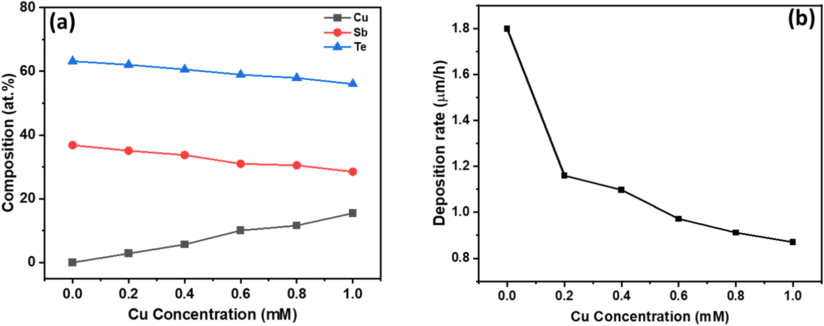
Based on these voltammetry studies, a fixed potential of −150 mV is chosen for the co-deposition from all the baths. The homogeneous distribution of constituent elements is critical for the formation of the CuSbTe ternary alloy and its optimized thermoelectric properties such as the Seebeck coefficient and electrical conductivity. EDX spectral analysis is used to validate the uniform distribution and elemental compositions of the binary and ternary alloys. Fig. S1 of the ESI† depicts the corresponding EDX spectra of each sample. Table S1† shows typical atomic composition values for the EDX spectra captured at five different regions of the films. The average chemical composition of the electrodeposited films as a function of bath Cu concentration is shown in Fig. 2(a). In the absence of Cu in the electrolyte, the deposited Sb2Te3 film has a composition of 36.83 at% Sb and 62.17 at% Te, which is close to the Sb2Te3 ideal stoichiometry.30 As the Cu concentration increased in the electrolyte, the Cu content in the deposited film increased gradually (almost linearly), while the Sb and Te contents significantly decreased. In the film deposited from the 1 mM Cu bath, the amount of Sb is reduced by 22.7%, while the Te content is lowered by 11.3%. This finding is consistent with the anomalous co-deposition of the CuSbTe ternary alloy. These EDX results support the hypothesis that during co-deposition, Sb is replaced by Cu in the Sb2Te3 lattice. However, the mechanism of Cu co-deposition is still unknown, necessitating further investigation. Fig. 2(b) illustrates the deposition rate of different films as a function of Cu concentration in the electrolytes. The rate at which the films are being deposited is substantially reduced as the Cu content rises. The deposition rate in the Sb2Te3 bath is 1.8 μm h−1, but it is 0.87 μm h−1 in the 1 mM Cu-content bath, which infers that the less noble Cu deposit limits the growth of Sb2Te3 during co-deposition. Thus, as the amount of Cu content in the electrolyte increases, the reverse sweep current density decreases as can be seen in the CV curves. This result demonstrates that the addition of Cu causes the dissolution of Sb and Te in the bath, thus significantly weakening the Sb2Te3 formation process. On the other hand, the deposition of more noble Sb/Te is suppressed in the presence of less noble Cu ions by co-deposition and thereby the deposition rate of Sb2Te3 decreases to a certain extent at higher Cu concentration.31–33
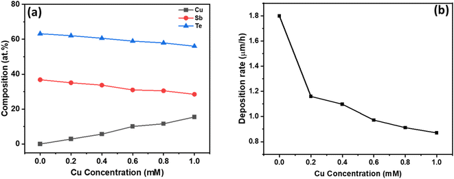 |
| | Fig. 2 (a) Elemental composition of electrodeposited films with respect to Cu concentration in the electrolyte, (b) deposition rate of electrodeposited films with respect to different Cu concentrations. | |
3.2 Structural properties
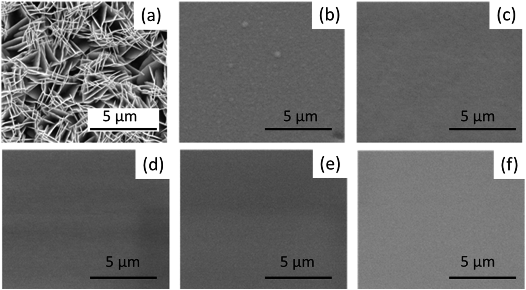
Fig. 3(a–f) show the surface morphology of the Sb2Te3 and the CuSbTe films containing different Cu concentrations. The Sb2Te3 films appear to be porous with plate-like morphology (Fig. 3(a)). Ternary CuSbTe films (b–f), on the other hand, are denser and uniform. The Cu co-deposition increases ultra-disperse characteristic features in the deposit and forms the supersaturated solid solutions (SSS).34 The ability of alloys to form the SSS structure is related to the atomic radius mismatch between the constituent ions and their valence electron range. This means that the attraction between different atoms is higher than similar atoms, which changes the reaction kinetics and is prone to form SSS. Therefore, the extensity of the base Sb2Te3 structure is observed during Cu co-deposition.34
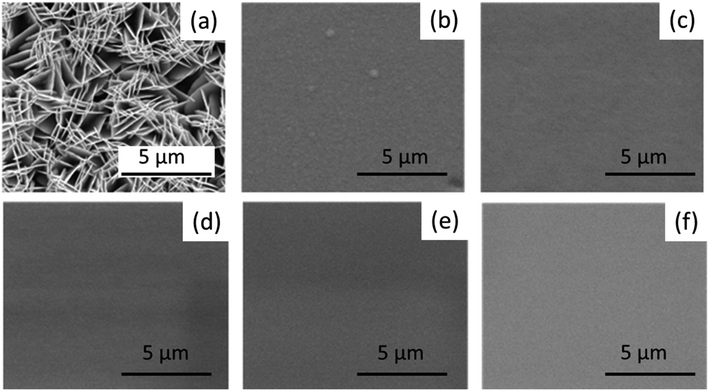 |
| | Fig. 3 (a–f) SEM images of Sb2Te3 and ternary CuSbTe thin films: (a) Sb2Te3, (b) Cu0·2SbTe, (c) Cu0·4SbTe, (d) Cu0·6SbTe, (e) Cu·8SbTe, and (f) Cu1·0SbTe. | |
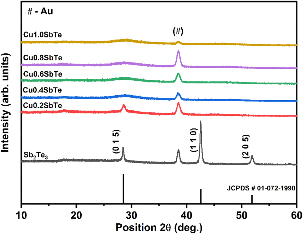
To further investigate the effect of Cu incorporation, all the samples are subjected to X-ray diffraction analysis. The typical X-ray diffraction patterns for as-deposited binary Sb2Te3 and ternary CuSbTe thin films are shown in Fig. 4. The binary Sb2Te3 film exhibits diffraction peaks at 28°, 42° and 52° confirming the formation of a thermoelectrically favourable c-axis oriented rhombohedral (R![[3 with combining macron]](https://www.rsc.org/images/entities/char_0033_0304.gif) m space group) crystal structure.35,36 The film is strongly orientated in the (110) direction as compared to the (015) direction and can be indexed to the corresponding standard pattern of the crystalline Sb2Te3 hexagonal closed pack layered structure (JCPDS #01-072-1990). The other peak at 38° is due to the Au seed layer used for the electrodeposition,20 which is observed in each film. In the case of ternary Cu0·2SbTe, the preferential orientation of the (110) plane disappears, and only a less intense (015) orientation is observed, indicating that Cu co-deposition inhibits the growth of Sb2Te3 crystallites at the (110) plane.37 The (015) peak shifts toward higher 2θ and broadens due to the addition of more Cu, implying anomalous variation in the lattice parameter. It is interesting to note that as the copper content in the film increased, the crystal structure completely collapsed, implying that the film had transitioned from crystalline to amorphous. This is primarily due to the small ionic radius of Cu, which enters the Sb2Te3 lattice, particularly in the (110) plane direction, and creates extra lattice stress along the layers, resulting in the observed crystalline to amorphous phase transition. According to Hoang et al.,38 the inclusion of Cu in the Sb–Te–Sb chains may disturb the hybridized Sb and Te p bands, resulting in a rearrangement in the density of states by dragging states at the Fermi level to lower energy. As a result, abnormal crystal structures emerge during co-deposition.38
m space group) crystal structure.35,36 The film is strongly orientated in the (110) direction as compared to the (015) direction and can be indexed to the corresponding standard pattern of the crystalline Sb2Te3 hexagonal closed pack layered structure (JCPDS #01-072-1990). The other peak at 38° is due to the Au seed layer used for the electrodeposition,20 which is observed in each film. In the case of ternary Cu0·2SbTe, the preferential orientation of the (110) plane disappears, and only a less intense (015) orientation is observed, indicating that Cu co-deposition inhibits the growth of Sb2Te3 crystallites at the (110) plane.37 The (015) peak shifts toward higher 2θ and broadens due to the addition of more Cu, implying anomalous variation in the lattice parameter. It is interesting to note that as the copper content in the film increased, the crystal structure completely collapsed, implying that the film had transitioned from crystalline to amorphous. This is primarily due to the small ionic radius of Cu, which enters the Sb2Te3 lattice, particularly in the (110) plane direction, and creates extra lattice stress along the layers, resulting in the observed crystalline to amorphous phase transition. According to Hoang et al.,38 the inclusion of Cu in the Sb–Te–Sb chains may disturb the hybridized Sb and Te p bands, resulting in a rearrangement in the density of states by dragging states at the Fermi level to lower energy. As a result, abnormal crystal structures emerge during co-deposition.38
 |
| | Fig. 4 XRD patterns of Sb2Te3 films with increased copper content. | |
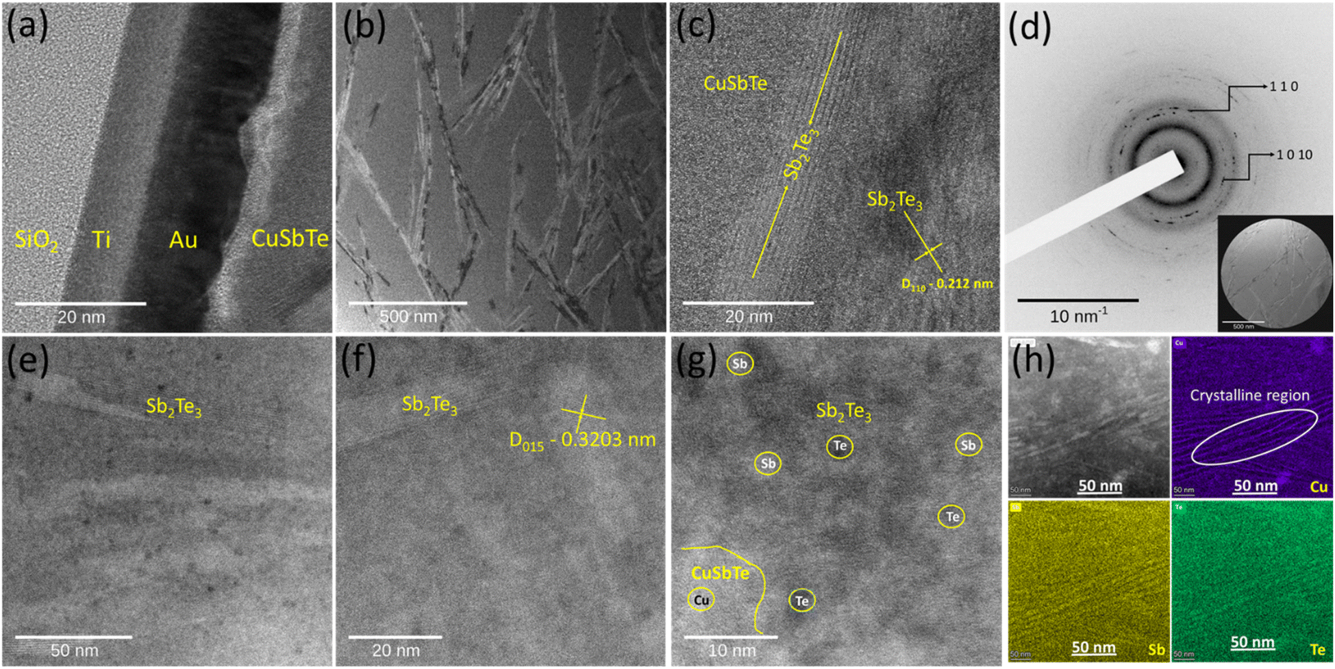
The localized microstructure of ternary CuSbTe and the crystalline to amorphous transformation of the sample are further analysed using a high-resolution transmission electron microscope (JEOL 2100FE HRTEM). An ultrathin, Cu0·4SbTe lamella is prepared in an FIB STEM [TESCAN SOLARIS] and examined by high-angle annular dark field scanning TEM (TITAN THEMIS S/TEM). Fig. 5(a–c) illustrate the HRTEM images of the Cu0·4SbTe lamella with different magnifications. During Cu co-deposition, Cu creates lattice disorder in Sb2Te3 lattices, which breaks the crystal symmetry. Fig. 5(a) shows the order of thin film layers on a Si substrate followed by electrodeposited CuSbTe thin films. HR-TEM images in Fig. 5(b) and (c) show the presence of needle like Sb2Te3 nano-crystallites within the amorphous matrix. In contrast to the crystalline region, the amorphous region has a higher volume fraction as shown in Fig. 5(b). This indicates that the amorphization happens as a result of competing transformation kinetics, in which the stable crystalline phase and the metastable amorphous phase both grow simultaneously. However, because the rate of creation of the amorphous phase is substantially higher than that of the crystalline phase, the resultant phase is amorphous in the initial stage of transition. This results in the formation of supersaturated solid solutions (SSS) with low range crystalline order.34 A basic crystalline structure may be seen in Fig. 5(c), where distinct lattice fringes are connected by tiny parallel lines. The measured d-spacing value of 3.2 Å is consistent with the (015) orientation of pristine Sb2Te3 [JCPDS #01-072-1990], further confirming the existence of a stable crystalline phase along with a metastable amorphous phase. The corresponding selected area electron diffraction (SAED) pattern shown in Fig. 5(d) further reveals the formation of diffused rings along with intense dots confirming that the films are more amorphous in nature with polycrystalline Sb2Te3 crystallites at the grain boundaries. The comprehensive HRTEM observation of the CuSbTe shown in Fig. S2(a–f)† further demonstrates the presence of structural defects in the form of dislocations. As shown in Fig. S2a,† some base crystalline regions separated by grain boundaries still exist in the film. A random change in image contrast, depicted in Fig. S2b,† indicates the disordered crystal structure. The dark contrast region, however, exhibits lattice fringes connected to the underlying Sb2Te3 crystalline structure. Fig. S2c† reveals the presence of dislocations in the crystalline region, which may be due to the induced stress during co-deposition. According to the Fast-Fourier Transform (FFT) pattern seen in Fig. S2(a–c),† the base crystalline structure is rhombohedral Sb2Te3. Fig. S2(d–e)† resemble amorphous-crystalline features with dislocations at grain boundaries. In contrast to crystalline diffraction, the Cu-rich region exhibits a diffused diffraction pattern in Fig. S2f,† confirming the large volume fraction of amorphous structure. Further investigation in the SSS region (Fig. 5(e–g)) reveals the presence of Sb2Te3 crystallites. The HAADF-STEM image (Fig. 5f & g) further validates the distribution of heavy metal (Cu & Sb) in the films. Fig. 5(h) depicts the corresponding elemental mapping in the Cu0·4SbTe sample and confirms the distribution of Cu throughout the amorphous matrix except in needle-like Sb2Te3 crystallites. This means that the created dimensional vacancy leads to local distortions (i.e. dislocations) in the crystal lattice. When the lattice deformation is considerably changed the atom stable positions result in the formation of metastable phases.34 The observed structural disordering can therefore be primarily attributed to substantial lattice dislocations, which result in crystalline-to-amorphous phase change during co-deposition.
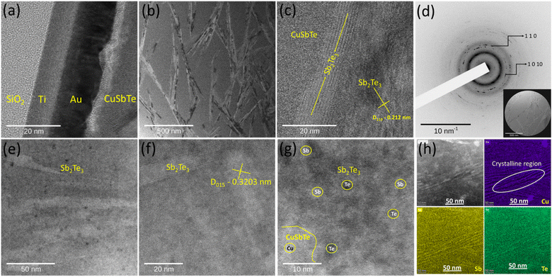 |
| | Fig. 5 (a) HRTEM image of the Cu0·4SbTe film on the Si/SiO2/Ti/Au Substrate, (b) distribution of amorphous and crystalline fractions of CuSbTe, (c) individual lattice fringes of the base Sb2Te3 crystalline structure within the amorphous matrix, (d) SAED pattern of Cu0·4SbTe in the spotted region of the inset, (e) HAADF-STEM image showing Sb2Te3 in CuSbTe, (f) d-spacing value of (0 1 5) orientation, (g) high magnification image showing selected crystalline spots and (h) selected HAADF_STEM image and the corresponding EDS mapping of elements Cu, Sb and Te. | |
3.2.1 Raman analysis.
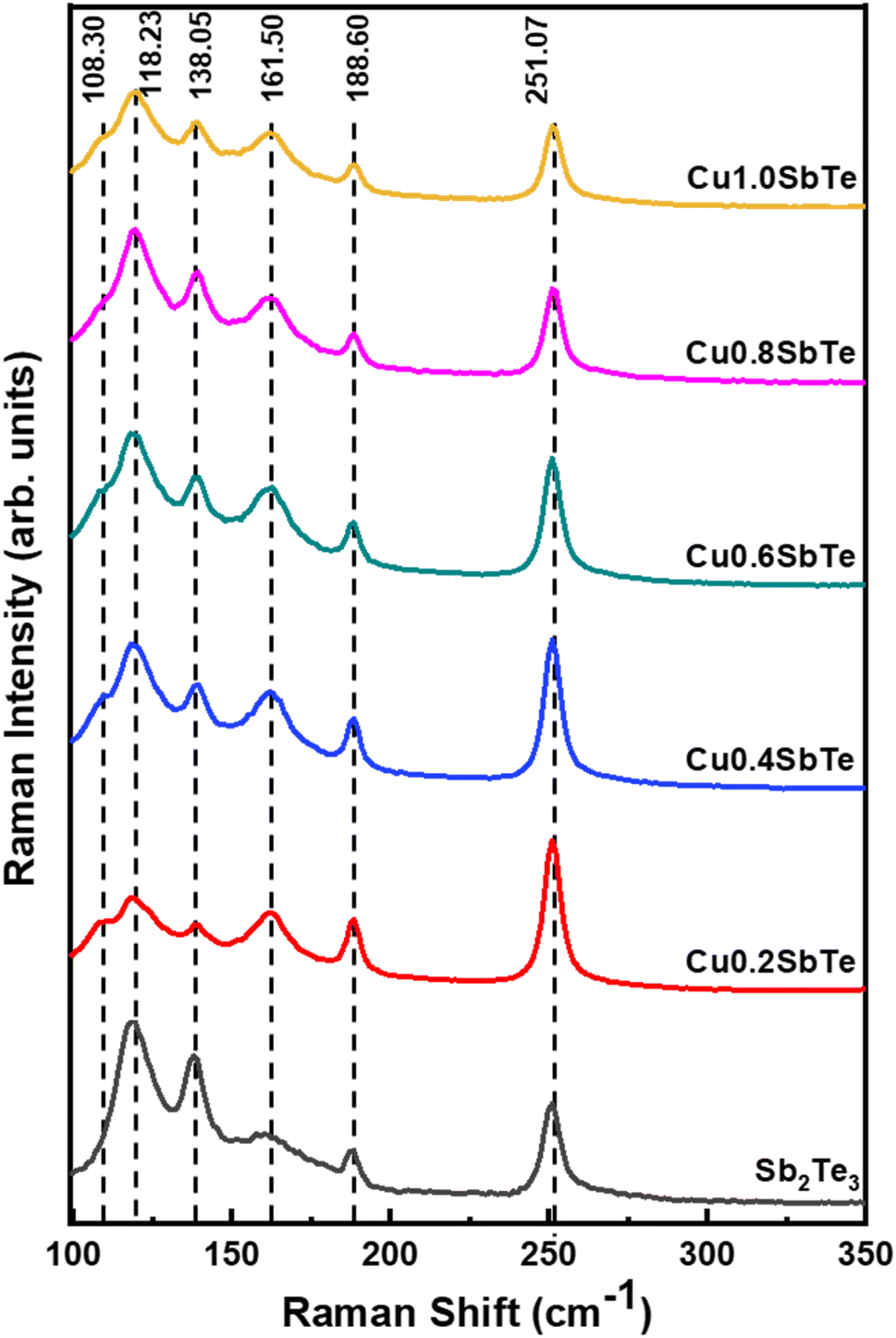
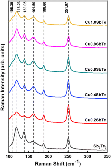
The surface oxidation and purity of the electrodeposited films could be further evaluated using Raman measurements ranging from 100 cm−1 to 350 cm−1 for all films, as shown in Fig. 6. Binary Sb2Te3 and ternary CuSbTe have very similar Raman spectra, indicating an underlying Sb2Te3 rhombohedral crystal structure. For the binary Sb2Te3, six peaks are noticed at 108, 118, 138, 161, 188, and 251 cm−1. The two peaks at 108 and 161 cm−1 are closely related to the Sb2Te3 E2g and A1g modes.13 The peak at 138 cm−1 corresponds to the Te–Te E2 mode,39 while the peak at 118 cm−1 represents the Te–Te A1 mode. The two peaks at 188 and 251 cm−1 should be associated with the Sb–O vibration mode of the surface oxide layer formed by antisite defects.39,40 The Raman spectra show no discernible change with the addition of Cu, indicating the anomalous co-deposition of CuSbTe. However, varied intensity of the Raman peaks is found because of the creation of a disordered or amorphous structure. The intensity of the Sb–O bond vibrations is particularly high at low Cu concentrations up to 0.4 mM and weakens as the Cu concentration increases. This suggests that the diffusion of Cu into the Sb lattice site along the c-axis results in the creation of antisite defects by producing more Sb2O3 up to that concentration.40 Beyond 0.4 mM, the intensity of the Sb–O vibrations decreases as Cu-rich phase formation takes place in the deposited films. These results are consistent with XRD results as discussed earlier.
 |
| | Fig. 6 Room temperature Raman scattering spectra of Sb2Te3 and ternary CuSbTe thin films. | |
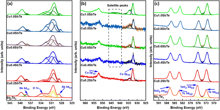
3.2.2 XPS analysis.
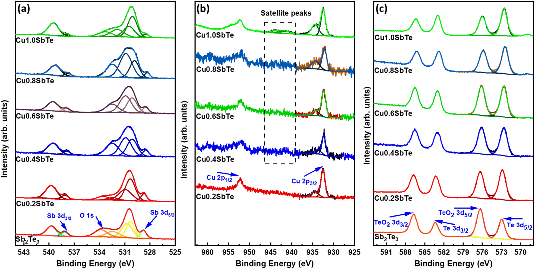
The XPS analysis is an effective method for determining the oxidation states and stoichiometry of elements. Fig. S3† of the ESI† shows XPS survey spectra of Sb2Te3 and other CuSbTe, confirming the presence of Cu 2p, Sb 3d, and Te 3d energy levels. The core-level Sb 3d XPS spectra are depicted in Fig. 7(a). Because of the overlaying binding energies, it is difficult to distinguish the Sb 3d and O1s energy states. Two significant deconvoluted peaks with binding energies of 538.10 and 528.70 eV (an energy split of 9.4 eV) are consistent with Sb3+ in the Sb2Te3 (Sb 3d3/2 and Sb 3d5/2, respectively).41 Meanwhile, the two peaks at 539.7 and 530.5 eV are caused by Sb2O3 formation at the surface and can be assigned to the O 1s energy level.42,43 The creation of a native oxide layer, on the other hand, was verified further by the core level Te 3d XPS spectra, as shown in Fig. 7(c). It shows two peaks at binding energies of 583.37 and 572.92 eV, corresponding to the Te 3d3/2 and 3d5/2, respectively with a spin–orbit splitting of 10.5 eV. These finding are consistent with the literature.20,44,45 The Cu addition significantly shifts the Te3d binding energies to the lower side; obviously, the shift is larger for high Cu concentrations. This is owing to the fact that the less electronegative atoms replace any of the high electronegative atoms in the crystal lattice.35 Obviously, Cu has a lower electronegativity of 1.90 than Sb (2.05) and Te (2.1), and therefore it can easily replace either Sb or Te in the Sb–Te lattices.36 Other prominent Te 3d peaks at 586.72 and 576.32 eV indicate the native surface oxide layer of TeO2.46 The figure clearly illustrates that as the Cu concentration increases, the intensity ratio of Te–O binding energies decreases while metallic Te increases. However, the predicted Sb![[thin space (1/6-em)]](https://www.rsc.org/images/entities/char_2009.gif) :Te ratio is 2:3, which indicates that an excess of Sb and Te is present in the film surface in their oxide form. This suggests that the Cu-induced amorphous phase transition generates a more native oxide layer in addition to surface oxidation caused by atmospheric exposure.41,47 As a result, the films should be stored and handled under inert gas conditions to avoid surface oxidation processes. To better understand the Cu-energy states within the Sb2Te3 lattices, the core level Cu 2p XPS spectra are collected and shown in Fig. 7(b). The primary energy level splitting for Cu 2p3/2 and Cu 2p1/2 is 932.48 and 952.28 eV, respectively, separated by 19.8 eV, implying a prominent Cu+ state.43 With higher Cu concentrations, the Cu 2p3/2 binding energies split into two peaks, with a new peak at 934.5 eV representing the Cu2+ oxidation state, whereas, the corresponding 2p1/2 peaks exhibit higher broadening due to the Auger process associated with the decay of the core hole state present in the main 2p shell or simply Coster–Kronig effect.48 The Cu2+/1+ splitting is more prevalent in Cu1·0SbTe, indicating that there is excess Cu oxidation. Furthermore, satellite peaks between 940 and 944 eV imply a high ratio of the Cu2+ oxidation state. Therefore, Cu may easily replace either Sb or Te, and an excess of native oxide layer forms on the film surface.20
:Te ratio is 2:3, which indicates that an excess of Sb and Te is present in the film surface in their oxide form. This suggests that the Cu-induced amorphous phase transition generates a more native oxide layer in addition to surface oxidation caused by atmospheric exposure.41,47 As a result, the films should be stored and handled under inert gas conditions to avoid surface oxidation processes. To better understand the Cu-energy states within the Sb2Te3 lattices, the core level Cu 2p XPS spectra are collected and shown in Fig. 7(b). The primary energy level splitting for Cu 2p3/2 and Cu 2p1/2 is 932.48 and 952.28 eV, respectively, separated by 19.8 eV, implying a prominent Cu+ state.43 With higher Cu concentrations, the Cu 2p3/2 binding energies split into two peaks, with a new peak at 934.5 eV representing the Cu2+ oxidation state, whereas, the corresponding 2p1/2 peaks exhibit higher broadening due to the Auger process associated with the decay of the core hole state present in the main 2p shell or simply Coster–Kronig effect.48 The Cu2+/1+ splitting is more prevalent in Cu1·0SbTe, indicating that there is excess Cu oxidation. Furthermore, satellite peaks between 940 and 944 eV imply a high ratio of the Cu2+ oxidation state. Therefore, Cu may easily replace either Sb or Te, and an excess of native oxide layer forms on the film surface.20
 |
| | Fig. 7 XPS spectra for (a) Sb 3d, (b) Cu 2p and (c) Te 3d for the as-deposited binary Sb2Te3 and ternary CuSbTe thin films. | |
To validate the formation of the native oxide layer, the depth profile XPS spectra of Cu0·4SbTe are recorded after Ar-etching at different times, and the results are shown in Fig. S4 of the ESI.† The core level XPS spectra of Sb 3d indicate that the intensity of the O 1s peak decreases as the etching progresses, and after about 750 seconds (s) of surface etching, the oxygen intensity at 531–532 eV is minimal, indicating that the oxide is present within only a few tens of nanometres from the film's surface. On the other hand, the Cu 2p depth profile reveals that the Cu2+ state decreases with increasing etching time, implying that the Cu2+ state is only available near the film's surface. Similarly, in Te 3d spectra, the intensity of peaks related to TeO2 decreases with etching time and completely disappears after 750 S. Thus, from the depth profile, it can be concluded that oxide states of Cu, Sb and Te only exist at the surface of the films as a result of the Cu-induced crystalline to amorphous phase transformation and the prolonged exposure of the films to the atmosphere.
3.3 Thermoelectric properties
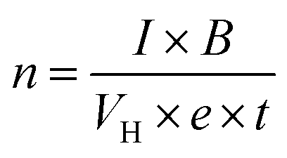
The electrical and thermal transport properties of the pristine Sb2Te3 and CuSbTe thin films are assessed by employing in-plane Hall and Seebeck measurements at room temperature. Fig. 8(a–c) depict the thermoelectric transport properties of all the films as a function of Cu concentration in the electrolytes. The Hall measurement determines the carrier concentration, carrier mobility and electrical conductivity of the films. Obviously, the measured negative Hall voltage suggests the majority of n-type charge carriers in the as deposited films. The carrier concentration (n) is derived from eqn (3):49| |  | (3) |
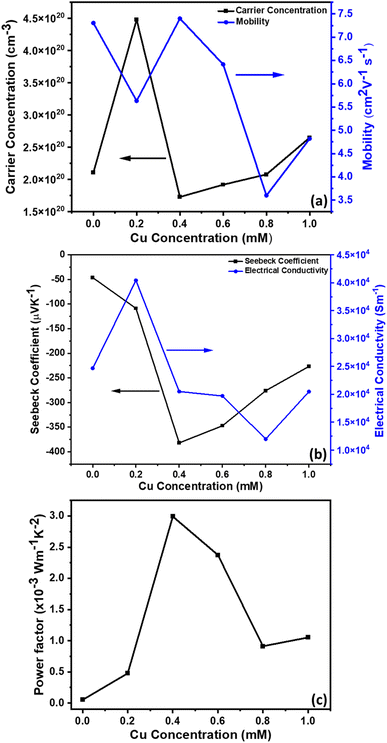 |
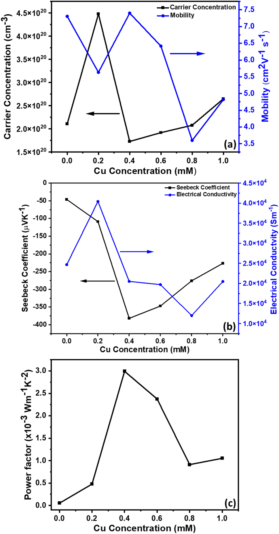
| | Fig. 8 (a) Carrier concentration and hall mobility with respect to Cu concentration, (b) in-plane Seebeck and electrical conductivity vs. Cu concentration and (c) calculated power factor of the films for different Cu concentrations. | |
In eqn (3), n denotes the charge carrier concentration, I the current, B the magnetic field, VH the Hall voltage, e the electron charge and t the film thickness. The variations of charge carrier concentration (n) and mobility (μ) with the Cu concentrations are shown in Fig. 8(a). It is worth noting that the addition of Cu during co-deposition results in a dramatic change in carrier concentration and mobility due to the change in various concentrations of defects by Cu inclusion. As-deposited binary Sb2Te3 shows a high mobility of 7.30 cm2 V−1 s−1 with a carrier concentration of 2.1 × 1020 cm−3. As the Cu content increases, the crystallinity of the films decreases as shown in the XRD results (Fig. 4). The disordered crystal structure varies with the concentration of antisite defects and grain boundaries, which results in the formation of trapping states. These trapping states are capable of trapping carriers and thus lead to a decrease in the mobility.50 Moreover, the creation of these antisite defects leads to an increase in the carrier concentration. Thus, films with 0.2 mM Cu concentration show slightly low mobility and the highest carrier concentration of 4.48 × 1020 cm−3. In the 0.4 mM Cu concentration film, the VTe vacancies are more dominant defects than the antisite one. Therefore, the mobility increases again, whereas the carrier concentration decreases sharply. Beyond 0.4 mM Cu concentration, the mobility starts to fall down and shows a slight increment for 1 mM Cu concentration, which might be again due to the formation of the CuSbTe alloy with large volume fraction.
The electrical conductivities of these films are calculated from the carrier concentration and mobility using the following equation:19
where
σ is the electrical conductivity,
n is the carrier concentration,
e is the electron charge and
μ is the mobility.
Fig. 8(b) shows that the electrical conductivity of the binary Sb
2Te
3 and ternary CuSbTe films ranges in the order of 1.3 × 10
−4- 4.0 × 10
−4 S m
−1. Due to its high carrier concentration and adequate mobility, Cu0·2SbTe has the highest electrical conductivity (4.0 × 10
−4 S m
−1) when compared to other ternary CuSbTe alloys. To our surprise, larger Cu concentrations result in lowered electrical conductivity due to their low carrier concentration and limited mobility. The observed physical attributes could be directly connected to the Cu-induced structural disorder. During co-deposition, the random arrangement of Cu and Sb atoms in the lattices, as well as the creation of antisite defects, result in nonlinear fluctuations in the physical properties. Tailoring of the Cu/Sb ratio in the CuSbTe system can regulate the density of states near the Fermi level, resulting in differences in the electrical and thermoelectric properties. The electrical transport of the disordered semiconductor can be explained using the Anderson–Mott model.
14 According to this model, the disordered electron states exhibit carrier transport in their localized states
via hopping, resulting in low conductivity and carrier mobility at higher Cu concentrations. It has been recognized that pristine Sb
2Te
3 is fundamentally p-type due to native antisite (Sb
Te) imperfections.
10,51 These faults, however, are extremely sensitive to the fabrication process. The used electrodeposition leads to the formation of a native oxide phase at grain boundaries, which may affect the primary carrier type in Sb
2Te
3, resulting in an n-type carrier for our binary Sb
2Te
3 with considerably low carrier concentration and high mobility. As is generally known, carrier concentration is extremely sensitive to atomic-scale point defects. It has been experimentally proven that the insertion of Cu under various conditions into 2D layered structures such as Sb
2Te
3, Bi
2Te
3, or Bi
2Se
3 can result in various kinds of lattice defects.
52 The Cu atom may easily diffuse through the basal plane direction of the Sb
2Te
3 crystal structure during the electrodeposition process and acts as a donor. After entering the lattice, Cu atoms can exist as interstitial defects or as substitutes for Sb and/or Te atoms. However, because of a small difference in electronegativity between Te (2.1) and Sb (2.05), Sb may easily move from Sb-sites to Te-sites to produce antisite defects, each of which contributes one hole as a free carrier.
10 However, our experimental results contradict the preceding assumptions by exhibiting n-type characteristics regardless of Cu concentration. This suggests that acceptor-like antisite defects are not significant in our case. On the other hand, the rapid diffusion of Cu into SbTe and the formation of Sb
2O
3 may have a considerable effect on the Seebeck coefficient and power factor.
40 The surface Sb
2O
3 limits the formation of Sb
Te antisite defects, and more Cu diffusion leads to the Te sublimation by forming CuSbTe and creates excess V
Te, which contributes two electron carriers. Thereby, all the samples behave as n-type, and show a high negative Seebeck coefficient. Similarly, after the inclusion of Cu, all the films exhibited more n-type features with significant swings in carrier concentrations and mobility. Among the various Cu-concentrations, Cu0·4SbTe has the lowest carrier concentration (1.73 × 10
20 cm
−3) and the maximum mobility (7.39 cm
2 V
−1 s
−1), both of which have an effect on electrical conductivity. The Cu co-deposition generated non-stoichiometry in Sb
2Te
3, probably changing the defect density
via the formation of disordered structure at higher Cu concentrations, and thereby causing further reduction in carrier mobility and electrical conductivity.
14 This could be attributed to Cu-induced complex bond formation in Sb–Te lattices, driven by Cu substitution in both Sb and Te sites, which results in the disordered crystal structure, as supported by XRD studies.
53 As shown in
Fig. 8(b), Seebeck coefficients (
S) of all the samples exhibit negative values indicating n-type thermoelectric transport. Generally, the amorphous thin films show higher Seebeck coefficient values as compared to single crystalline bulk materials. Because in the amorphous materials, the density of states is localized at the Fermi level so the carrier movements happen only by hopping from one localized state to another. The Seebeck coefficient for an amorphous thin film is given by:
54| |  | (5) |
where
S is the Seebeck coefficient,
kB is the Boltzmann constant,
e is the electronic charge,
T is the absolute temperature and
σ (
E) is the electrical conductivity determined as a function of energy (
E). The binary Sb
2Te
3 film shows the lowest Seebeck coefficient of −46 μV K
−1. Interestingly, the addition of Cu increases the
S for samples deposited up to 0.4 mM, and decreases with further increase of Cu. A maximum
S of −382 μV K
−1 was observed for Cu0·4SbTe and this may be due to the inverse effect of the carrier concentration. The carrier concentration of the 0.4 mM sample is 1.7 × 10
20 cm
−3, which is almost 3 times lower than that of Cu0·2SbTe, resulting in the highest Seebeck coefficient of −382 μV K
−1 among all the films. The large volume fraction of the crystalline to amorphous phase transition induced microstructure in CuSbTe actively reduces this carrier concentration and thus leads to a high Seebeck value. The formation of Cu-rich amorphous CuSbTe with underlying grain boundary Sb
2Te
3 precipitates (as seen from TEM in
Fig. 5) results in enriched Te vacancies (V
Te) and free electrons, which resulted in n-type Seebeck coefficients for all the samples.
10 To further validate the materials' thermoelectric applications, the power factor (
S2σ) is calculated for all the electrodeposited films at room temperature.
Fig. 8(c) depicts the calculated power factor values for the samples as a function of Cu concentration in the baths. It demonstrates that Cu-alloyed Sb
2Te
3 possesses higher power factor values than the binary Sb
2Te
3 film. The film with 5.7 at% Cu (Cu0·4SbTe) has the maximum power factor of 2.8 mW m
−1 K
−2, which is almost 20 times greater than the Sb
2Te
3 film at ambient temperature. So, adjusting the carrier concentration with a change in the Cu level in the Sb
2Te
3 films helps to optimize the power factor by balancing the Seebeck coefficient and electrical conductivity.
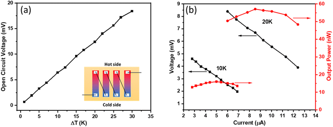
3.4 Flexible thermoelectric generator (TEG)
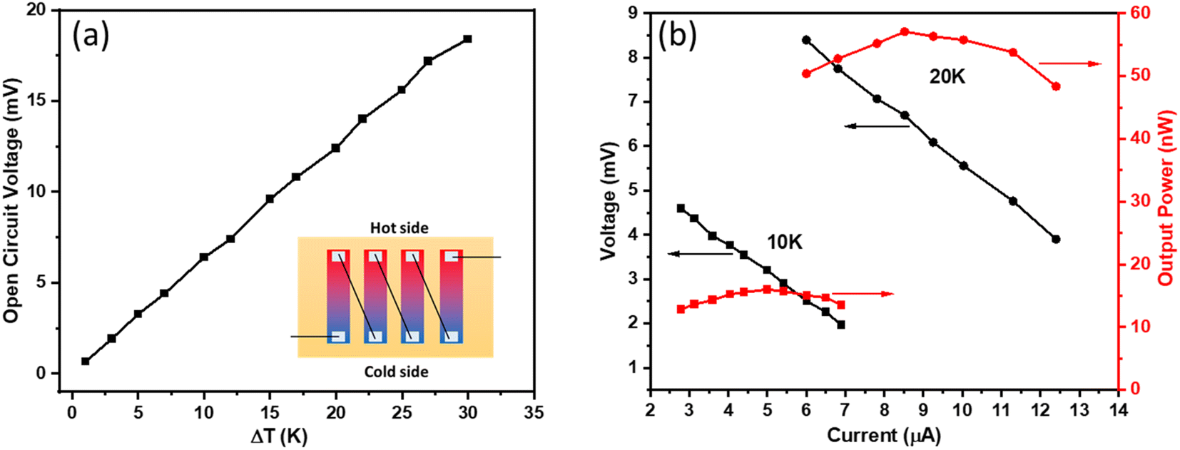
The Cu0·4SbTe film is grown directly onto a conductive Nylon fiber to test its performance as a uni-leg TEG. The Fig. 9(a) inset shows the schematic of a simple prototype of a flexible TEG made up of four legs (each with a 20 × 5 mm2 area) connected by copper wires coated with Ag paste. A temperature gradient (ΔT) is created by placing this thermoelectric device on top of two Peltier modules and by keeping the temperature at 20 °C at the cold side. Fig. 9(a) shows the open circuit voltage as a function of temperature gradient (ΔT), which increases linearly as ΔT increases.
 |
| | Fig. 9 (a) The open circuit voltage at different temperature gradients (ΔT), and (b) the output voltage and power versus current at different ΔT. | |
An open circuit voltage of 3.2, 6.4, 12.4 and 18.4 mV is achieved for a ΔT of 5, 10, 20, and 30 K, respectively. Fig. 9(b) shows the output voltage and power versus current for two different temperature gradients of 10 and 20 K; where the output voltage is inversely proportional to the output current. Here, the output power (P) is calculated using the following equation:55
| |  | (6) |
where
Rin is the internal resistance of the device and
Rex is the load resistance. A maximum power (
Pmax) is obtained when the external load resistance matches the internal resistance of the TEG devices. The
Pmax values for a Δ
T of 10, 20 and 30 K are 16, 57 and 120 nW, respectively. The output power of our flexible device is comparable to the previously reported work, as shown in
Table 1. The output voltage and power can be raised further by improving the electrodeposition conditions on the nylon membrane and by increasing the number of legs.
Table 1 Comparison of thermoelectric performances of flexible films (all measurements are done at room temperature)
| Materials |
V
oc (mV) |
P
max (nW) |
ΔT(K) |
N (No. of legs) |
Ref. |
| PC/Cu7Te4/PC/Te |
31.2 |
94.7 |
39.1 |
8 |
56
|
| PI/AgBiSbTe |
18.3 |
55.9 |
30 |
4 |
57
|
| Kapton PI/Cu2Se |
3.84 |
3.31 |
38 |
10 |
58
|
| MWCNTs-SnSe/PEDOT:PS |
2.7 |
13.5 |
30 |
4 |
59
|
| Sb2Se3/β-Cu2Se/PANI |
7.9 |
80.1 |
30 |
5 |
60
|
| PVDF/Ag2Se |
5.86 |
4.9 |
30 |
5 |
61
|
| Nylon/Cu0.4SbTe |
18.4 |
120 |
30 |
4 |
This work |
4. Conclusions
In summary, Cu-alloyed Sb2Te3 films are successfully grown using an electrodeposition technique. With increasing Cu concentrations, a co-deposition driven crystalline to amorphous phase transition is demonstrated. The substantial amount of amorphous CuSbTe microstructure integrated with Sb2Te3 nanocrystallites tailors the carrier concentration and mobility. Adding excess Cu into Sb and Te sites can increase the Te vacancies and leads to strong n-type semiconducting nature. The film deposited from the 0.4 mM Cu containing bath shows a high Seebeck coefficient of −382 μV K−1 and power factor of 2.8 mW m−1 K−2. A prototype TEG is fabricated by depositing Cu0·4SbTe on a flexible Nylon fiber, which shows a power output of 120 nW at a temperature difference of 30 K. Thus, CuSbTe can be a promising candidate as an n-type thermoelectric material for near room temperature thermoelectric device applications.
Conflicts of interest
There are no conflicts to declare.
Acknowledgements
This work received funding from the European Union's Horizon 2020 Research and Innovation Programme under Grant Agreement No. 825114 (SmartVista). This publication has emanated from research supported in part by a research grant from Science Foundation Ireland (SFI) and is co-funded under the European Regional Development Fund under Grant Number 12/RC/2276.
References
- T. Ghosh, S. Roychowdhury, M. Dutta and K. Biswas, High-Performance Thermoelectric Energy Conversion: A Tale of Atomic Ordering in AgSbTe2, ACS Energy Lett, 2021, 6(8), 2825–2837, DOI:10.1021/acsenergylett.1c01184.
- G. J. Snyder and E. S. Toberer, Complex thermoelectric materials, Nat. Mater., 2008, 7(2), 105–114, DOI:10.1038/nmat2090.
- T. Wu, J. Kim, J.-H. Lim, M.-S. Kim and N. V Myung, Comprehensive Review on Thermoelectric Electrodeposits: Enhancing Thermoelectric Performance Through Nanoengineering, Front. Chem., 2021, 9, 762896, DOI:10.3389/fchem.2021.762896.
- M. Dutta, D. Sarkar and K. Biswas, Intrinsically ultralow thermal conductive inorganic solids for high thermoelectric performance, Chem. Commun., 2021, 57(39), 4751–4767, 10.1039/D1CC00830G.
- S. Prasad K,
et al., Tuning the thermoelectric properties by manipulating copper in Cu2SnSe3 system, J. Alloys Compd., 2018, 748, 273–280, DOI:10.1016/j.jallcom.2018.03.136.
- T. Shi, J. Zheng, X. Wang, P. Zhang, P. Zong and K. M. Razeeb, Recent advances of electrodeposition of Bi2Te3 and its thermoelectric applications in miniaturized power generation and cooling, Int. Mater. Rev., 2022, 1–35, DOI:10.1080/09506608.2022.2145359.
- B. L. Du, H. Li and X. F. Tang, Enhanced thermoelectric performance in Na-doped p-type nonstoichiometric AgSbTe2 compound, J. Alloys Compd., 2011, 509(5), 2039–2043, DOI:10.1016/j.jallcom.2010.10.131.
- R. Mohanraman, R. Sankar, F. C. Chou, C. H. Lee and Y.-Y. Chen, Enhanced thermoelectric performance in Bi-doped p-type AgSbTe2 compounds, J. Appl. Phys., 2013, 114(16), 163712, DOI:10.1063/1.4828478.
- L. Ferrer-Argemi, Z. Yu, J. Kim, N. V Myung, J.-H. Lim and J. Lee, Silver content dependent thermal conductivity and thermoelectric properties of electrodeposited antimony telluride thin films, Sci. Rep., 2019, 9(1), 9242, DOI:10.1038/s41598-019-45697-9.
- W.-S. Liu,
et al., Thermoelectric Property Studies on Cu-Doped n-type CuxBi2Te2.7Se0.3 Nanocomposites, Adv. Energy Mater., 2011, 1(4), 577–587, DOI:10.1002/aenm.201100149.
- R. Bhardwaj,
et al., Tin doped Cu3SbSe4: A stable thermoelectric analogue for the mid-temperature applications, Mater. Res. Bull., 2019, 113, 38–44, DOI:10.1016/j.materresbull.2019.01.010.
- Y. Sadia, D. Lumbroso and Y. Gelbstein, High-ZT Due to the Influence of Copper in Ti(Ni(1-x)Cu(x))Sn, Mater., 2023, 16(5) DOI:10.3390/ma16051902.
- S. Guo,
et al., Enhanced Crystallization Behaviors of Silicon-Doped Sb2Te Films: Optical Evidences, Sci. Rep., 2016, 6(1), 33639, DOI:10.1038/srep33639.
- J. Kim, J.-Y. Lee, J.-H. Lim and N. V Myung, Optimization of Thermoelectric Properties of p-type AgSbTe2 Thin Films via Electrochemical Synthesis, Electrochim. Acta, 2016, 196, 579–586, DOI:10.1016/j.electacta.2016.02.206.
- Y. Kimura,
et al., Solvothermal synthesis of n-type Bi2(SexTe1−x)3 nanoplates for high-performance thermoelectric thin films on flexible substrates, Sci. Rep., 2020, 10(1), 6315, DOI:10.1038/s41598-020-63374-0.
- D. W. Newbrook,
et al., Selective Chemical Vapor Deposition Approach for Sb2Te3 Thin Film Micro-thermoelectric Generators, ACS Appl. Energy Mater., 2020, 3(6), 5840–5846, DOI:10.1021/acsaem.0c00766.
- L. Yan,
et al., Highly Thermoelectric ZnO@MXene (Ti3C2Tx) Composite Films Grown by Atomic Layer Deposition, ACS Appl. Mater. Interfaces, 2022, 14(30), 34562–34570, DOI:10.1021/acsami.2c05003.
- P. Nieroda, A. Kusior, J. Leszczyński, P. Rutkowski and A. Koleżyński, Thermoelectric Properties of Cu2Se Synthesized by Hydrothermal Method and Densified by SPS Technique, Mater., 2021, 14(13) DOI:10.3390/ma14133650.
- S. Lal, D. Gautam and K. M. Razeeb, Optimization of annealing conditions to enhance thermoelectric performance of electrodeposited p-type BiSbTe thin films, APL Mater., 2019, 7(3), 31102, DOI:10.1063/1.5049586.
- N. Padmanathan, S. Lal, D. Gautam and K. M. Razeeb, Amorphous Framework in Electrodeposited CuBiTe Thermoelectric Thin Films with High Room-Temperature Performance, ACS Appl. Electron. Mater., 2021, 3(4), 1794–1803, DOI:10.1021/acsaelm.1c00063.
- S. Lal, K. M. Razeeb and D. Gautam, Enhanced Thermoelectric Properties of Electrodeposited Cu-Doped Te Films, ACS Appl. Energy Mater., 2020, 3(4), 3262–3268, DOI:10.1021/acsaem.9b02153.
- M. Y. Kim,
et al., Control of Cu-doping behavior in n-type Cu0.01Bi1.99Te2.7Se0.3 polycrystalline bulk via fabrication technique change, J. Mater. Res. Technol., 2021, 14, 765–771, DOI:10.1016/j.jmrt.2021.06.106.
- Y. Saiga, B. Du, S. K. Deng, K. Kajisa and T. Takabatake, Thermoelectric properties of type-VIII clathrate Ba8Ga16Sn30 doped with Cu, J. Alloys Compd., 2012, 537, 303–307, DOI:10.1016/j.jallcom.2012.05.049.
- F. Li, G. Jinghan, W. Wang and Y. Gong, Potentiodynamic Deposition of Cu Doped BixCuySb2 x yTez Thin Film as Thermoelectric Materials, Int. J. Electrochem. Sci., 2022, 17, 221055, DOI:10.20964/2022.10.57.
- J. Park, J. Seo, J.-H. Lim and B. Yoo, Synthesis of Copper Telluride Thin Films by Electrodeposition and Their Electrical and Thermoelectric Properties, Front. Chem., 2022, 10 DOI:10.3389/fchem.2022.799305.
- W. He,
et al., Multiple Effects Promoting the Thermoelectric Performance of SnTe by Alloying with CuSbTe2 and CuBiTe2, ACS Appl. Mater. Interfaces, 2021, 13(44), 52775–52782, DOI:10.1021/acsami.1c15614.
- T. J. Slade,
et al., Contrasting SnTe–NaSbTe2 and SnTe–NaBiTe2 Thermoelectric Alloys: High Performance Facilitated by Increased Cation Vacancies and Lattice Softening, J. Am. Chem. Soc., 2020, 142(28), 12524–12535, DOI:10.1021/jacs.0c05650.
- M. R. Burton, A. J. Naylor and I. S. Nandhakumar, Electrochemically copper-doped bismuth tellurium selenide thin films, Electrochem. Commun., 2018, 97, 56–59, DOI:10.1016/j.elecom.2018.10.006.
- L. I. Soliman, E. Soad, A. M. Abo, H. A. Zayed and S. A. El Ghfar, Structural and electrical properties of CuSbTe2, CuSbSe2 and CuSbS2 chalcogenide thin films, J. Exp. Theor. Phys., 2002, 11(4), 139–152 CAS.
- C. Schumacher,
et al., Optimization of Electrodeposited p-Doped Sb2Te3 Thermoelectric Films by Millisecond Potentiostatic Pulses, Adv. Energy Mater., 2012, 2(3), 345–352, DOI:10.1002/aenm.201100585.
- E. Vernickaite, N. Tsyntsaru and H. Cesiulis, Electrochemical co-deposition of tungsten with cobalt and copper: Peculiarities of binary and ternary alloys coatings formation, Surf. Coat. Technol., 2016, 307, 1341–1349, DOI:10.1016/j.surfcoat.2016.07.025.
- H. Nakano, M. Matsuno, S. Oue, M. Yano, S. Kobayashi and H. Fukushima, Mechanism of Anomalous Type Electrodeposition of Fe-Ni Alloys from Sulfate Solutions, Mater. Trans., 2004, 45(11), 3130–3135, DOI:10.2320/matertrans.45.3130.
- H. Dahms and I. M. Croll, The Anomalous Codeposition of Iron-Nickel Alloys, J. Electrochem. Soc., 1965, 112(8), 771, DOI:10.1149/1.2423692.
- V. V Povetkin and O. V Devyatkova, Formation of Metastable Phases in the Process of Electrodeposition of Metals and Alloys, Trans. IMF, 1996, 74(5), 177–178, DOI:10.1080/00202967.1996.11871121.
- Z. Zheng, P. Fan, J. Luo, G. Liang and D. Zhang, Enhanced Thermoelectric Properties of Antimony Telluride Thin Films with Preferred Orientation Prepared by Sputtering a Fan-Shaped Binary Composite Target, J. Electron. Mater., 2013, 42(12), 3421–3425, DOI:10.1007/s11664-013-2779-5.
- M. H. Jang,
et al., Effect of In incorporated into SbTe on phase change characteristics resulting from changes in electronic structure, Appl. Phys. Lett., 2010, 96, 52112 CrossRef.
- M. Xia, K. Ding, F. Rao, X. Li, L. Wu and Z. Song, Aluminum-Centered Tetrahedron-Octahedron Transition in Advancing Al-Sb-Te Phase Change Properties, Sci. Rep., 2015, 5(1), 8548, DOI:10.1038/srep08548.
- K. Hoang, S. D. Mahanti, J. R. Salvador and M. G. Kanatzidis, Atomic Ordering and Gap Formation in Ag-Sb-Based Ternary Chalcogenides, Phys. Rev. Lett., 2007, 99(15), 156403, DOI:10.1103/PhysRevLett.99.156403.
- K. A. Kokh, V. V Atuchin, T. A. Gavrilova, N. V Kuratieva, N. V Pervukhina and N. V Surovtsev, Microstructural and vibrational properties of PVT grown Sb2Te3 crystals, Solid State Commun., 2014, 177, 16–19, DOI:10.1016/j.ssc.2013.09.016.
- Z.-W. Sun,
et al., Stoichiometric Effect of Sb2Te3 Thin Film on Thermoelectric Property, ACS Appl. Energy Mater., 2022, 5(6), 7026–7033, DOI:10.1021/acsaem.2c00657.
- N. Kraft, G. Wang, H. Bryja, A. Prager, J. Griebel and A. Lotnyk, Phase and grain size engineering in Ge-Sb-Te-O by alloying with La-Sr-Mn-O towards improved material properties, Mater. Des., 2021, 199, 109392, DOI:10.1016/j.matdes.2020.109392.
- N. Theekhasuk,
et al., Improving the thermoelectric properties of thick Sb2Te3 film via Cu doping and annealing deposited by DC magnetron sputtering using a mosaic target, Curr. Appl. Phys., 2021, 31, 7–15, DOI:10.1016/j.cap.2021.07.011.
- T. J. Whittles,
et al., Core Levels, Band Alignments, and Valence-Band States in CuSbS2 for Solar Cell Applications, ACS Appl. Mater. Interfaces, 2017, 9(48), 41916–41926, DOI:10.1021/acsami.7b14208.
- J. Kim, K. H. Lee, S.-D. Kim, J.-H. Lim and N. V Myung, Simple and effective fabrication of Sb2Te3 films embedded with Ag2Te nanoprecipitates for enhanced thermoelectric performance, J. Mater. Chem. A, 2018, 6(2), 349–356, 10.1039/C7TA09013G.
- A. Singh,
et al., Systematic Study of Ferromagnetism in CrxSb2−xTe3 Topological Insulator Thin Films using Electrical and Optical Techniques, Sci. Rep., 2018, 8(1), 17024, DOI:10.1038/s41598-018-35118-8.
- L. V. R. Marcos, S. M. P. Kalaiselvi, O. Bin Leong, P. K. Das, M. B. H. Breese and A. Rusydi, Optical constants and absorption properties of Te and TeO thin films in the 13-14 nm spectral range, Opt. Express, 2020, 28(9), 12922–12935, DOI:10.1364/OE.381883.
- J. Schaumann,
et al., Improving the zT value of thermoelectrics by nanostructuring: tuning the nanoparticle morphology of Sb2Te3 by using ionic liquids, Dalton Trans., 2017, 46(3), 656–668, 10.1039/C6DT04323B.
- R. Nyholm, N. Martensson, A. Lebugle and U. Axelsson, Auger and Coster-Kronig broadening effects in the 2p and 3p photoelectron spectra from the metals 22Ti-30Zn, J. Phys. F: Met. Phys., 1981, 11(8), 1727, DOI:10.1088/0305-4608/11/8/025.
- N. K. Singh, S. Bathula, B. Gahtori, K. Tyagi, D. Haranath and A. Dhar, The effect of doping on thermoelectric performance of p-type SnSe: Promising thermoelectric material, J. Alloys Compd., 2016, 668, 152–158, DOI:10.1016/j.jallcom.2016.01.190.
- Z.-L. Wang, T. Araki, T. Onda and Z.-C. Chen, Effect of annealing on microstructure and thermoelectric properties of hot-extruded Bi–Sb–Te bulk materials, J. Mater. Sci., 2018, 53(12), 9117–9130, DOI:10.1007/s10853-018-2211-x.
- H.-J. Wu and W.-T. Yen, High thermoelectric performance in Cu-doped Bi2Te3 with carrier-type transition, Acta Mater., 2018, 157, 33–41, DOI:10.1016/j.actamat.2018.07.022.
- A. Vaško, L. Tichý, J. Horák and J. Weissenstein, Amphoteric nature of copper impurities in Bi2Se3 crystals, Appl. Phys., 1974, 5(3), 217–221, DOI:10.1007/BF00928132.
- J. Sun, H. Shi, T. Siegrist and D. J. Singh, Electronic, transport, and optical properties of bulk and mono-layer PdSe2, Appl. Phys. Lett., 2015, 107(15), 153902, DOI:10.1063/1.4933302.
- V. Damodara Das, N. Soundararajan and M. Pattabi, Electrical conductivity and thermoelectric power of amorphous Sb2Te3 thin films and amorphous-crystalline transition, J. Mater. Sci., 1987, 22(10), 3522–3528, DOI:10.1007/BF01161452.
- M. M. Mallick,
et al., High Figure-of-Merit Telluride-Based Flexible Thermoelectric Films through Interfacial Modification via Millisecond Photonic-Curing for Fully Printed Thermoelectric Generators, Adv. Sci., 2022, 9(31), 2202411, DOI:10.1002/advs.202202411.
- Y. Lu,
et al., Preparation and Characterization of Te/Poly(3,4-ethylenedioxythiophene):Poly(styrenesulfonate)/Cu7Te4 Ternary Composite Films for Flexible Thermoelectric Power Generator, ACS Appl. Mater. Interfaces, 2018, 10(49), 42310–42319, DOI:10.1021/acsami.8b15252.
- H. Shang,
et al., High-Performance Ag-Modified Bi0.5Sb1.5Te3 Films for the Flexible Thermoelectric Generator, ACS Appl. Mater. Interfaces, 2020, 12(6), 7358–7365, DOI:10.1021/acsami.9b21771.
- X.-L. Huang,
et al., High-performance copper selenide thermoelectric thin films for flexible thermoelectric application, Mater. Today Energy, 2021, 21, 100743, DOI:10.1016/j.mtener.2021.100743.
- D. Liu,
et al., Facile MWCNTs-SnSe/PEDOT:PSS ternary composite flexible thermoelectric films optimized by cold-pressing, J. Mater. Res. Technol., 2021, 15, 4452–4460, DOI:10.1016/j.jmrt.2021.10.075.
- M. Kim, D. Park and J. Kim, Thermoelectric Generator Using Polyaniline-Coated Sb2Se3/β-Cu2Se Flexible Thermoelectric Films, Polymers, 2021, 13, 1518, DOI:10.3390/polym13091518.
- H. Zhou, Z. Zhang, C. Sun, H. Deng and Q. Fu, Biomimetic Approach to Facilitate the High Filler Content in Free-Standing and Flexible Thermoelectric Polymer Composite Films Based on PVDF and Ag2Se Nanowires, ACS Appl. Mater. Interfaces, 2020, 12(46), 51506–51516, DOI:10.1021/acsami.0c15414.
|
| This journal is © The Royal Society of Chemistry 2023 |
Click here to see how this site uses Cookies. View our privacy policy here. 
 Open Access Article
 This Open Access Article is licensed under a Creative Commons Attribution-Non Commercial 3.0 Unported Licence
 *
*