
 Open Access Article
 This Open Access Article is licensed under a Creative Commons Attribution-Non Commercial 3.0 Unported Licence
An efficient approach for controlling the crystallization, strain, and defects of the perovskite film in hybrid perovskite solar cells through antisolvent engineering†
Nikolaos
Tzoganakis
a,
Konstantinos
Chatzimanolis
a,
Emmanuel
Spiliarotis
a,
George
Veisakis
a,
Dimitris
Tsikritzis
 *ab and
Emmanuel
Kymakis
ab
*ab and
Emmanuel
Kymakis
ab
aDepartment of Electrical & Computer Engineering, Hellenic Mediterranean University (HMU), Heraklion 71410, Crete, Greece. E-mail: dtsikritzis@hmu.gr
bInstitute of Emerging Technologies (i-EMERGE) of HMU Research Center, Heraklion 71410, Crete, Greece
First published on 26th July 2023
Abstract
The efficiency and stability of perovskite solar cells are regulated by defects at the grain boundaries and at the surface of organic–inorganic halide perovskite films. Various methods have been proposed to improve the quality of the perovskite film, but most of these approaches complicate the fabrication procedure. Here, we show an efficient and simple engineering approach for regulating the crystallization, strain, and defects of the perovskite film by adding the organic salt octylammonium bromide (OABr) in the antisolvent solution. The proposed treatment improves the crystallization of the perovskite film, controls the strain in the film, and efficiently passivates defects of the hybrid quadruple cation perovskite, reducing the charge trap density and non-radiative recombination. Consequently, the non-radiative losses in the optimized OABr treated devices were considerably mitigated by 43.6%, allowing a Voc of 1.16 V and efficiency up to 20.4% to be achieved. In addition, the stability of the OABr treated devices was improved, retaining 80% of their initial performance under ambient conditions for more than 1400 hours.
1. Introduction
Perovskite solar cells (PSCs) have made significant advances during the last ten years, and their power conversion efficiency (PCE) has increased from 3.8% to 25.7%.1,2 The high absorption coefficient, long carrier diffusion length, and variable band gap are only a few of the outstanding photoelectric features of hybrid organic–inorganic halide perovskite materials that contributed to such remarkable efficiency.3,4 Following the generation of light-induced charge carriers inside the perovskite layer in a typical PSC, these carriers are separated and transported to charge transport layers (CTLs).5–7 In order for this mechanism to be efficient, a low density of bulk and interfacial trap states is required. Extensive research has shown that although the perovskite is defect tolerant,8 the interfaces with CTLs exhibit a high density of defects that induce high surface recombination velocity, limiting the open circuit voltage, Voc, and the performance of PSCs.9,10 An effective method to reduce the recombination at perovskite/CTLs interfaces is to postprocess the pre-formed perovskite layer's surface with a suitable material. Surface traps are typically eliminated by forming a passivation layer consisting of organic or inorganic materials.11–14 However, this approach adds an extra layer in the device, complicating the fabrication procedure, increasing the cost, and limiting the selection of suitable layers that can be deposited over the perovskite film. Another engineering approach is to create a two-dimensional (2D) Ruddlesden–Popper perovskite on top of a three-dimensional (3D) perovskite.15–17 Creating 2D–3D perovskite heterojunctions on the surfaces of 3D perovskites via cation exchange has recently been shown to be an excellent method for improving the performance and stability of PSCs.18–20 Moreover, various alkali chain organic salts such as n-butylammonium bromide, n-hexylammonium bromide, and n-octylammonium bromide, were employed as precursors to form 2D perovskites through the post-treatment of 3D perovskite surfaces.21–23 Although numerous efforts have been made, it is still difficult to form a high-quality 2D/3D interconnection.24 In addition, treatment of the perovskite surface with hydrophobic long chain alkylammonium salts can reduce surface energy of the perovskite that can affect the overlayer growth.25The effective passivation of defects along with improved stability under ambient conditions has been demonstrated through the incorporation of large alkyl-ammonium spacer cations, such as alkylammonium, butylammonium, and phenylethylammonium, on the perovskite surface.26–28 Among the plethora of available alkylammonium halide salts, octylammonium iodide (OAI) was used for surface treatment of perovskites forming 2D/3D perovskite phases29 increasing PCE and stability.30,31 Octylammonium bromide (OABr) has been used in normal PSCs as a passivation agent by surface treatment of the perovskite layer. Specifically, N. Mozaffari et al. have shown that using OABr in conjunction with guanidinium bromide for the surface treatment of perovskites increased the performance via the formation of 1D/2D phases and defect passivation.21 Furthermore, OABr, OAI, and octylammonium chloride (OACl) were compared in the article by M. A. Mahmud et al. and it was shown that they increased the performance, although OACl proved more efficient.32 Similarly, OABr, OAI and phenethylammonium iodide (PEAI) were used for the treatment of the perovskite surface.33 The authors showed that the surface treatment slightly increased the performance of PSCs, but the thermal stress of the devices can promote diffusion of cations, forming 1D/2D phases, and prolonging thermal stress can lead to a loss in crystallinity near the perovskite surface, increased non-radiative recombination, and reduced performance. In the work of J. J. Yoo et al. OABr and shorter alkylammonium bromide salts were used in normal PSCs, which resulted in 2D phases on the perovskite surface and higher PCE. The OABr treated devices exhibited a champion Voc of 1.17 V.34 In a similar approach, OABr and salts with varying alkylammonium chain lengths were used as surface passivation agents on wide band-gap PSCs.35 The authors identified the formation of various phases at the perovskite surface upon the application of the passivation agents. At the topmost layer, an ultrathin unreacted alkylammonium organic cation resides, whereas beneath it exists a thin pure two-dimensional (2D) perovskite intermixed with the three-dimensional (3D) perovskite. The best performing devices were achieved with OABr. The article by S. Y. Kwon et al. describes the application of OABr, OAI, and OACl on the perovskite surface under regulated humidity conditions.36 The authors found that the application of octylammonium salts had a small positive effect on the device performance, and at high humidity, the Cl− ions can cause serious damage to the device. It is noteworthy that all these studies feature the application of alkylammonium halide salts as a surface treatment of perovskite surface only in normal PSCs. Our findings demonstrate that the conventional method of utilizing OABr as a surface passivation layer on the perovskite has an adverse effect on the growth of PC61BM and it cannot be adopted in inverted PSCs. However, we show that OABr can be implemented in inverted PSCs through antisolvent engineering.
Antisolvent engineering consists of adding a functional molecule in the antisolvent in order to improve the quality of the perovskite layer.37 Organic molecules and polymers were the first functional additives that were added in the antisolvent due to their good solubility in Chlorobenzene (CB) and toluene, the most common antisolvents. For example, the polymer PMMA was dissolved in mixed CB/toluene solvents as a templating agent to control nucleation and crystal growth, forming perovskite films with high electrical quality.38 In 2016, Han et al. utilized PCBM for the first time to create a graded heterojunction between a perovskite and PCBM, using a one-step antisolvent fabrication method to achieve a controlled fullerene distribution.39 Subsequently, other approaches were presented, including mainly organic molecules40–42 and perovskite quantum dots,43–45 but also polymers.46
In the present study, we employ OABr for the first time in inverted PSCs, by inserting OABr in an antisolvent mixture. This approach does not interfere with the growth of PC61BM and increases the performance and stability of inverted PSCs. Specifically, we introduced the organic halide salt octylammonium bromide (OABr) in the antisolvent solution and dropped it onto the perovskite to promote crystallization with the aim of regulating the top region of the perovskite film during the crystallization process. The OABr in the antisolvent affected the crystallization of the perovskite, greatly enhancing the crystallinity of the resulting layer and increasing the grain size. In addition, this strategy reduced the trap density and regulated strain in the perovskite film. As a result, the non-radiative recombination was suppressed, the device's Voc was raised from 1.023 to 1.160 V, and the PCE improved from 17.73% to 20.40%. Furthermore, the perovskite surface was made more hydrophobic with the OABr treatment, thus significantly increasing the humidity and heat stability of the PSCs.
2. Materials and methods
2.1 Device fabrication
Prepatterned glass/Indium Tin Oxide (ITO) substrates were cleaned using an ultrasonic bath with deionized water, acetone, and isopropyl alcohol, respectively, for 15 min in each step. The samples were then transferred to an N2 glove box, where they underwent UV ozone treatment for 15 min. A poly[bis(4-phenyl)(2,4,6-trimethylphenyl)amine (PTAA) layer (Solaris, Mw = 20–70 kDa) was prepared by spin coating a PTAA solution in toluene (2 mg mL−1), at an angular speed of 6000 rpm for 30 s, and afterwards films were annealed at 110 °C for 10 min. The perovskite solution was prepared with the nominal stoichiometry Rb0.05Cs0.04(MA0.15FA0.85)0.91Pb(I0.90Br0.10)3 as in our previous studies.47,48 The perovskite layers were dynamically spin-coated onto the PTAA substrates at 6000 rpm for 45 s. At 20 s before the end of the spinning process, 200 mL of an anhydrous chlorobenzene (CB): isopropanol (IPA) (9![[thin space (1/6-em)]](https://www.rsc.org/images/entities/char_2009.gif) :1 v/v) (99.8%, Sigma Aldrich, 99.8%, Acros Organics) mixture was dropped onto the spinning perovskite film. For OABr (TCI) treated samples, solutions with different concentrations of OABr (0.01–0.25 mg mL−1) in CB/IPA (9:1 v/v) were prepared and used as antisolvent. The devices that implement OABr as a surface passivation layer over the perovskite were prepared by dispensing 50 μL of OABr solutions prepared in anhydrous IPA at concentrations of 1 and 2 mg mL−1 on the perovskite surface and spin coating at a rotating speed of 4000 rpm for 45 s. Then the samples were annealed at 100 °C for 10 minutes on a preheated hotplate. Next, the samples were immediately annealed for 45 min on a preheated hotplate at 100 °C. A thin layer of PC61BM (99%, Solenne), approximately 30 nm thick, was deposited by spin coating a 20 mg mL−1 PC61BM solution in anhydrous CB onto the perovskite at 2000 rpm for 60 s. Afterwards, 45 μL of a 0.5 mg mL−1 bathocuproine (BCP) solution (96%, Sigma Aldrich) prepared in IPA (99.5% extra dry, ACROS Organics) was dispersed and spin coated onto PC61BM at 4000 rpm for 45. Finally, a 100 nm-thick Ag top electrode was deposited by thermal evaporation in a high vacuum of 10−6 mbar.
:1 v/v) (99.8%, Sigma Aldrich, 99.8%, Acros Organics) mixture was dropped onto the spinning perovskite film. For OABr (TCI) treated samples, solutions with different concentrations of OABr (0.01–0.25 mg mL−1) in CB/IPA (9:1 v/v) were prepared and used as antisolvent. The devices that implement OABr as a surface passivation layer over the perovskite were prepared by dispensing 50 μL of OABr solutions prepared in anhydrous IPA at concentrations of 1 and 2 mg mL−1 on the perovskite surface and spin coating at a rotating speed of 4000 rpm for 45 s. Then the samples were annealed at 100 °C for 10 minutes on a preheated hotplate. Next, the samples were immediately annealed for 45 min on a preheated hotplate at 100 °C. A thin layer of PC61BM (99%, Solenne), approximately 30 nm thick, was deposited by spin coating a 20 mg mL−1 PC61BM solution in anhydrous CB onto the perovskite at 2000 rpm for 60 s. Afterwards, 45 μL of a 0.5 mg mL−1 bathocuproine (BCP) solution (96%, Sigma Aldrich) prepared in IPA (99.5% extra dry, ACROS Organics) was dispersed and spin coated onto PC61BM at 4000 rpm for 45. Finally, a 100 nm-thick Ag top electrode was deposited by thermal evaporation in a high vacuum of 10−6 mbar.
2.2 Material characterization
Atomic force microscopy (AFM) images were captured using an XE7 microscope (Park Systems) by operating in tapping mode. Water contact angle measurements were performed on an Ossila L2004A1 goniometer. Ambient photoemission spectroscopy (APS) and Kelvin probe measurements were performed with an APS04 N2-RH system (KP Technology) to estimate the work function (WF) and the valence band (VB). More specifically, the contact potential difference (CPD) was measured using a vibrating Kelvin probe tip coated with a gold alloy (2 mm in diameter). The absolute WF of the tip was estimated to be around 4.54 ± 0.06 eV, which was calibrated by measuring a silver reference and calculating its absolute WF by APS. The VB of the materials was determined using a UV light excitation source (D2) in the range of 3.8–6 eV and extrapolating the cube root of the photoemission signal to zero. The conduction band (CB) level of the perovskite was calculated using the equation: CB = VB + Eg,PV where Eg,PV is the photovoltaic band gap as estimated from the external quantum efficiency (EQE) measurements. The samples were kept and prepared in the dark for surface photovoltage (SPV) measurements. First, the WF in the dark was monitored until a stable signal was reached. Then, the sample was illuminated with white light (20 mW cm−2) for 100 s and the SPV decay was recorded for another 100 s. Steady-state and time-resolved photoluminescence measurements (PL and TRPL) were performed using an FS5 spectrofluorometer (Edinburgh Instruments). A pulsed laser diode (l = 478.4 nm, pulse full-width at half maximum 70 ps, and repetition rate 200 kHz–40 MHz) was used to excite the samples. Transient photovoltage and transient photocurrent measurements were performed with a commercial apparatus (Arkeo, Cicci Research s.r.l.) based on a high-speed waveform generator that drives a high-speed LED (5000 K). The device is connected to a trans-impedance amplifier and a differential voltage amplifier to monitor short-circuit current or open-circuit voltage. The light intensity from the pulse is varied between 0.001 and 2 suns equivalent. The hole trap density of perovskite films without and with the OABr cation was measured by the space-charge-limited-current (SCLC) method using a hole only diode configuration of ITO/PTAA/Perovskite/Spiro-OMeTAD/Au. For transient photovoltage, the perturbation produced using the LED was less than 10% of the background-applied light bias. Transient photocurrent measurements were performed under large perturbations (duty cycle 0.3) for a time duration of 400 μs. The devices were connected to a 50 Ω and 1 MΩ resistor for TPC and TPV measurements, respectively. J–V characteristics of devices were measured using a solar simulator (Oriel), equipped with a 450 W Xenon lamp and an AM1.5G filter. The intensity of the lamp was calibrated at 100 mW cm−2 using a KG-5 windowed Si reference cell. The devices were evaluated inside an N2 filled glovebox and the J–V curves were recorded with a multiplexor test board system (Ossila) by scanning from −0.1 V to 1.2 V, with a scan rate of 10 mV s−1 and a voltage step of 10 mV. A metal mask was used to define the active area of the solar cells (0.04 cm2). EQE was measured with the QE-R2 system from Enlitech, at a chopping frequency of 65 Hz. The X-ray diffraction (XRD) measurements were obtained using a RIGAKU D/MAX 2500 powder diffractometer with Cu Ka radiation. The scanning electron microscopy (SEM) images were acquired using a JEOL 700F system. The stability measurements were conducted with the InfinityPV ISOS testing laboratory equipment, operating in ISOS-L2 mode. The devices were encapsulated using a piece of glass and a UV-curable epoxy as an adhesive (Ossila E132). Then, the devices were transferred to a testing chamber where they were exposed to continuous illumination at 1 sun and a temperature above 65 °C. Humidity was kept at 10–15%. The apparatus is equipped with a solar simulator using a metal halide source simulating the AM1.5G spectrum in the range 300–900 nm. The light intensity was calibrated at 100 mW cm−2 using a Si reference cell. The devices were held in an open circuit between measurements.3. Results
3.1 Characterization of PSCs
The proposed engineering approach that employs OABr during perovskite crystallization is depicted in Fig. 1a. The OABr powder was dissolved in the CB/IPA solvent mixture and dripped over the perovskite layer during the final stages of the spin-coating procedure. This antisolvent step initiated the crystallization of the perovskite layer, which was finalized with the annealing step that followed. The treatment of the perovskite with OABr during the antisolvent step affected the crystallization of the perovskite layer, the surface morphology, and the energetics at the interfaces with the charge transport layers. Thus, the OABr treatment influenced the performance of the PSCs, depending on the concentration of OABr in the antisolvent solution.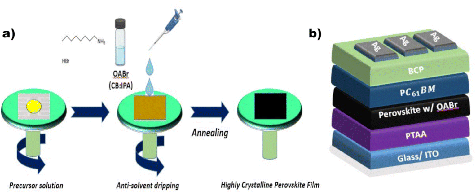 | ||
| Fig. 1 (a) Experimental procedure for the preparation of a perovskite film employing the organic salt OABr in the antisolvent step. (b) Schematic structure of the inverted perovskite solar cell manufactured in this work. | ||
To assess the direct impact of OABr on the photovoltaic performance, we fabricated inverted PSC devices (Fig. 1b) in which different percentages of OABr were diluted in the antisolvent mixture. Fig. 2 shows the performance of the resulting devices along with the main photovoltaic parameters: power conversion efficiency (PCE), fill factor (FF), open circuit voltage (Voc), and short circuit current density (Jsc) in panels a–d, respectively. Moreover, in Table 1 the mean photovoltaic parameters and the best performing devices are listed. The photovoltaic parameters were extracted from the corresponding J–V curves. Fig. S1a† shows the forward and the reverse J–V scans of the reference and best performing OABr devices and in Fig. S1b† the stabilized current density curves at fixed voltage are shown. The hysteresis is minimal in both devices.
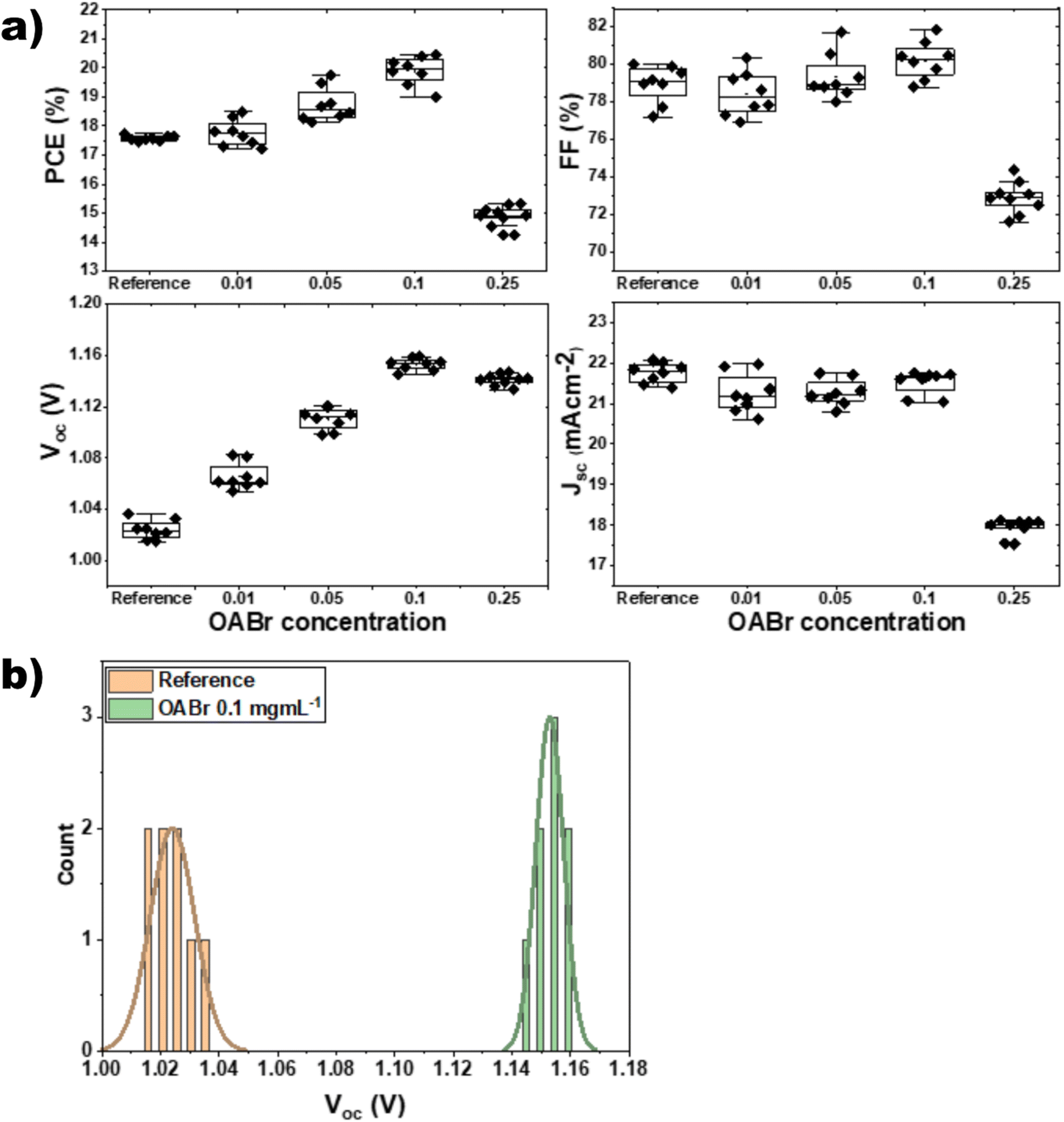 | ||
| Fig. 2 (a) Evolution of the photovoltaic parameters with increasing OABr concentrations in the antisolvent mixture. (b) Statistical distribution of Voc from eight reference and OABr treated PSCs. | ||
| Sample | PCE [%] | FF [%] | V oc [V] | J sc [mA cm−2] |
|---|---|---|---|---|
| Reference | 17.58 ± 0.09 | 78.91 ± 0.99 | 1.020 ± 0.002 | 21.75 ± 0.24 |
| (17.86) | (79.99) | (1.023) | (21.83) | |
| OABr 0.01 mg mL−1 | 17.75 ± 0.46 | 78.40 ± 1.17 | 1.061 ± 0.020 | 21.24 ± 0.48 |
| (18.49) | (77.80) | (1.082) | (21.97) | |
| OABr 0.05 mg mL−1 | 18.73 ± 0.59 | 79.31 ± 1.20 | 1.110 ± 0.002 | 21.27 ± 0.32 |
| (19.75) | (81.68) | (1.113) | (21.73) | |
| OABr 0.1 mg mL−1 | 19.89 ± 0.49 | 80.19 ± 0.99 | 1.150 ± 0.012 | 21.51 ± 0.29 |
| (20.40) | (81.14) | (1.160) | (21.68) | |
| OABr 0.25 mg mL−1 | 14.91 ± 0.34 | 72.90 ± 0.84 | 1.140 ± 0.002 | 17.93 ± 0.22 |
| (15.33) | (74.36) | (1.142) | (18.06) |
As shown in Fig. 2a and Table 1 the addition of OABr in the antisolvent mixture up to a concentration of 0.1 mg mL−1 increases PCE. For an optimal OABr concentration of 0.1 mg mL−1 the average PCE increases from 17.58 to 19.89% and the champion device achieves up to 20.4%. According to Table 1, the improvement in PCE is the result of a significant increase in Voc from 1.023 to 1.160 V, a 13.4% increase and a slight increase in the FF from 79.99 to 81.14%. The improvement in Voc is better visualized in Fig. 2b, where the histogram of the Voc values of the reference and the optimal OABr concentration are presented. With OABr treatment, the Voc increases, and the distribution is narrower compared to that of the reference. Interestingly, the Jsc of the best performing devices seems to decline with the addition of OABr. We will discuss this later. EQE measurements were performed to elucidate the photo-response of the devices. As shown in Fig. 3a, the EQE spectra of the reference and OABr treated samples exhibit different photo-responses at short and long wavelengths. The EQE spectrum of the 0.1 mg mL−1 OABr treated perovskite shows a lower photo-response at wavelengths around 700 nm, related to the interface recombination and low diffusion lengths at the perovskite/PC61BM interface.49,50 In contrast, at short wavelengths, the photo-response is enhanced, which indicates that light absorption is enhanced near the PTAA/perovskite interface. The EQE analysis indicates that the development of the PC61BM layer over the OABr treated perovskite is negatively affected, limiting the amount of OABr that can be added in the antisolvent mixture. Later in the manuscript we show that a high OABr concentration results in dewetting of PC61BM solution and to poor PC61BM film. However, the better photo-response of the OABr treated devices at shorter wavelengths is associated with the enhanced crystallinity of the perovskite and the better formation of the PTAA/perovskite interface, as will be shown next with the XRD and SEM measurements. The photovoltaic band gap (Eg,pv) can be estimated from the infection point of the EQE spectrum in the absorption threshold region, as shown in Fig. 3b.51 Interestingly, Eg,pv increases from 1.59 to 1.61 eV with OABr treatment, which collaborates with the reduction of Jsc. The absorption spectra of a perovskite film and a perovskite film treated with 0.1 mg mL−1 OABr are shown in Fig. S2a.† The Tauc plots (Fig. S2b†) derived from the absorption spectra confirm that the band gap of the perovskite increases with OABr treatment.
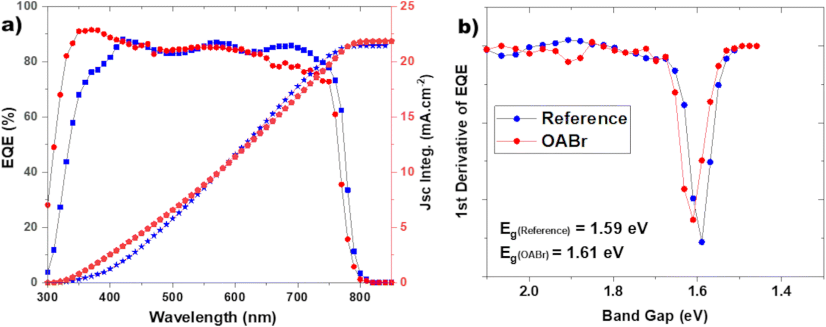 | ||
| Fig. 3 (a) EQE spectra of the reference and OABr treated champion devices. The integrated current density of the device's spectral response with the AM1.5G photon flux spectrum is depicted on the right axis. The integrated current density was calculated at 21.84 and 21.86 and mA cm−2 for the reference and OABr 0.1 mg mL−1, respectively. Panel (b) shows the first derivative of EQE. The Eg,pv for the reference and the 0.1 mg mL−1 OABr PSCs was estimated at 1.59 and 1.61 eV, respectively. | ||
3.2 Thin-film characterization
The significant improvement in the performance of PSCs with OABr must be correlated to the perovskite film. To this end, XRD measurements were performed to study the impact of OABr on perovskite film crystallization. Fig. 4a presents the diffraction pattern of the reference perovskite layer and of the 0.1 mg mL−1 OABr treated sample. The reference perovskite does not show a preferred orientation of the crystallites. In contrast to the reference sample, the optimum OABr sample shows higher peak intensity and preferential orientation for the (100) and (200) reflections. The sharp and narrow full width at half maximum (FWHM) of the (100) diffraction peak also supports the improved crystallinity of the OABr treated sample. The FWHM values with OABr were reduced to 0.15° compared to 0.35° for a pristine film. The average crystallite size D was calculated according to the Scherrer equation: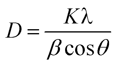 | (1) |
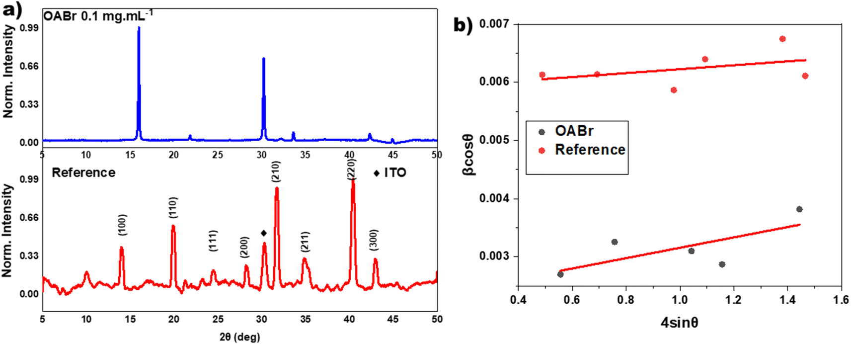 | ||
| Fig. 4 (a) The XRD diffraction pattern of a pristine perovskite film and the perovskite film treated with 0.1 mg mL−1 OABr and (b) the respective Williamson–Hall plots. The crystallite size was estimated at 24.6 and 63.8 nm for the reference and OABr samples, respectively. The strain was estimated at 3.4 × 10⁻³ for the reference and 8.9 × 10⁻³ for OABr. | ||
The morphological characteristics of the perovskite films were studied by SEM measurements. Fig. 5a and b show the top view SEM images of the reference and optimal OABr 0.1 mg mL−1 treated perovskite films, respectively. More top-view SEM images of perovskite films treated with increasing OABr concentrations are shown in Fig. S3.† It is evident that the morphology and grain size of the perovskite are affected by the OABr concentration. With increasing concentrations of OABr, grain boundaries are harder to distinguish and grain size increases. This is clearly visible at a maximum concentration of 0.25 mg mL−1 OABr, where the grain boundaries are barely distinguishable. The OABr concentration of 0.25 mg mL−1 resulted in a perovskite film with a very distinct morphology, large grains and almost no grain boundaries (Fig. S3e†). The mean grain size was calculated using the intersection count method. As shown in Table S1,† the mean grain size of the reference perovskite was around 180 ± 14 nm and increased to 244 ± 23 nm for the optimal OABr concentration and reached up to 487 ± 25 nm for the 0.25 mg mL−1 OABr concentration, which is twice the grain size of the reference. The cross-sectional SEM images in Fig. S3f and g† underline the improvement in perovskite layer formation with OABr. The reference sample shows poor perovskite formation close to the PTAA layer with pin-holes that limit the Voc and PCE. On the other hand, the 0.1 mg mL−1 OABr sample exhibits better grain formation and improved interface growth near PTAA. As we showed earlier, the higher EQE response of the 0.1 mg mL−1 OABr device at shorter wavelengths agrees with the morphology revealed from the SEM images.
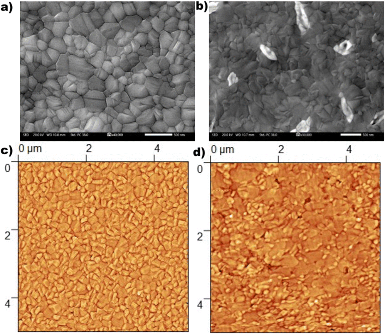 | ||
| Fig. 5 Top-view SEM images of (a) reference and (b) OABr 0.1 mg mL−1 treated perovskite films. The scale bar is 500 nm. 5 × 5 μm AFM topography images of (c) reference and (d) OABr 0.1 mg mL−1 treated perovskite films. The AFM images were processed to better visualize the perovskite grains. | ||
Complementary AFM topological measurements were conducted for complete morphological characterization of the perovskite films. Fig. S4† shows the AFM topography images of the reference sample and the perovskites treated with different percentages of OABr. In Fig. 5c and d the AFM images of the reference sample and of the 0.1 mg mL−1 OABr sample are presented, respectively. The topography of the films reveals the great impact of OABr in perovskite formation. The optimized OABr sample exhibited grains considerably larger than those of the reference. The surface roughness and the mean grain size values are tabulated in Table S2.† The mean grain size of the reference perovskite was estimated at 160 ± 12 nm and increased with the addition of OABr, reaching 270 ± 10 nm for the optimal 0.1 mg mL−1 concentration, in accordance with SEM analysis. However, the raw AFM images in Fig. S5† revealed that the perovskite layers with an OABr concentration greater than 0.05 mg mL−1 show a wave pattern with discrete hills and valleys, which indicate compression strain in the film. The XRD analysis also showed compressive strain in the perovskite film. Therefore, to observe the hill-valley morphology in the AFM images, the perovskite film is stressed uniformly parallel and perpendicular to the substrate. The AFM and SEM analyses indicate that OABr treatment increases the grain size, and therefore the grain boundaries, which act as recombination centers, are reduced. As a result, the non-radiative recombination and the charge extraction losses are expected to be considerably reduced, increasing Voc and PCE.
The surface of the perovskite samples was characterized with XPS to probe the chemical structure of the perovskite surface. Fig. S6† depicts the C 1s XPS core peak of the reference perovskite and of the perovskite treated with 0.1 mg mL−1 OABr. All the XPS spectra were referenced to the C 1s peak at 288.5 eV, which is assigned to C![[double bond, length as m-dash]](https://www.rsc.org/images/entities/char_e001.gif) N bonds of FA ions.54 The C 1s XPS core peak is analyzed for 3 major peak components, i.e., the peak assigned to C–C/CC bonds at 284.8 eV, the peak assigned to C–N bonds at 286.1 eV, and the peak assigned to CN bonds at 288.5 eV. Fig. S6c† shows the C 1s XPS core peak for the OABr sample. Interestingly, the C–C/CC peak is shifted to higher binding energies at 285.2 eV and the C–N peak at 286.5 eV due to the positively charged octylammonium cations. Fig. S7† shows the N 1s XPS core peaks of the reference sample and OABr. The reference sample shows one broad peak, which is ascribed to double and single carbon–nitrogen bonds due to the organic part of the perovskite, located at around 400.7 eV. In the N 1s spectrum of the OABr sample, in addition to the carbon–nitrogen peak, a contribution at higher BEs, at around 402.3 eV, is evident, which is ascribed to positively charged carbon–nitrogen bonds. XPS analysis of C 1s and N 1s peaks indicates that OABr treatment results in a high concentration of octylammonium cations at the surface of the perovskite layer. A high concentration of positive ions on the surface of the perovskite should decrease the WF, but we observed that the WF increases with the OABr concentration, as we will show next with the APS measurements. This can be rationalized if there is a dipole on the perovskite layer with the dipole moment facing toward the perovskite, i.e. there are negative Br− or I− ions over the octylammonium cations. CPD 2D mapping of the sample surface strengthens this argument. As shown in Fig. S8,† the CPD is unevenly distributed on the reference surface caused by the complex chemical structure of the perovskite. In contrast, the perovskite sample treated with OABr 0.1 mg mL−1 exhibits a higher WF and is more evenly disturbed on the surface, indicating a uniform potential and chemical environment. Therefore, based on XPS and CPD measurements, we postulate that near the perovskite surface (≈10 nm) there is a high concentration of octylammonium cations and at the outer surface of the perovskite there are Br− or I− counterions.
N bonds of FA ions.54 The C 1s XPS core peak is analyzed for 3 major peak components, i.e., the peak assigned to C–C/CC bonds at 284.8 eV, the peak assigned to C–N bonds at 286.1 eV, and the peak assigned to CN bonds at 288.5 eV. Fig. S6c† shows the C 1s XPS core peak for the OABr sample. Interestingly, the C–C/CC peak is shifted to higher binding energies at 285.2 eV and the C–N peak at 286.5 eV due to the positively charged octylammonium cations. Fig. S7† shows the N 1s XPS core peaks of the reference sample and OABr. The reference sample shows one broad peak, which is ascribed to double and single carbon–nitrogen bonds due to the organic part of the perovskite, located at around 400.7 eV. In the N 1s spectrum of the OABr sample, in addition to the carbon–nitrogen peak, a contribution at higher BEs, at around 402.3 eV, is evident, which is ascribed to positively charged carbon–nitrogen bonds. XPS analysis of C 1s and N 1s peaks indicates that OABr treatment results in a high concentration of octylammonium cations at the surface of the perovskite layer. A high concentration of positive ions on the surface of the perovskite should decrease the WF, but we observed that the WF increases with the OABr concentration, as we will show next with the APS measurements. This can be rationalized if there is a dipole on the perovskite layer with the dipole moment facing toward the perovskite, i.e. there are negative Br− or I− ions over the octylammonium cations. CPD 2D mapping of the sample surface strengthens this argument. As shown in Fig. S8,† the CPD is unevenly distributed on the reference surface caused by the complex chemical structure of the perovskite. In contrast, the perovskite sample treated with OABr 0.1 mg mL−1 exhibits a higher WF and is more evenly disturbed on the surface, indicating a uniform potential and chemical environment. Therefore, based on XPS and CPD measurements, we postulate that near the perovskite surface (≈10 nm) there is a high concentration of octylammonium cations and at the outer surface of the perovskite there are Br− or I− counterions.
The wettability and growth of overlayers are significantly influenced by the hydrophilicity of the substrate surface.32,33 Contact angle measurements were performed to characterize the wetting properties of the perovskite surface upon treatment with OABr. These measurements involve a droplet of PC61BM solution in CB (10 μL) being tracked as it changes over time on the test surface. Fig. S9† depicts the contact angle of the PC61BM solution in contact with thin films of (a) neat perovskite and perovskite treated with (b) 0.01 mg mL−1 OABr, (c) 0.5 mg mL−1 OABr, (d) 0.1 mg mL−1 OABr, and (e) 0.25 mg mL−1 OABr, respectively. As can be observed, the PC61BM droplet exhibits a contact angle of 29.1° on the reference perovskite, indicating the good wetting properties of the perovskite surface for the PC61BM layer formation. However, with an increasing amount of OABr in the anti-solvent solution the contact angle of the PC61BM droplet increases to 45.1° for the lowest OABr concentration and to 91.2° for the highest OABr concentration, which can lead to extensive PC61BM dewetting.
3.3 Steady state and transient measurements
Fig. 6 shows the steady-state photoluminescence (PL) and space-charge-limited current (SCLC) measurements, which were carried out to further investigate the light absorption and charge carrier behaviors in perovskite films. Notably, as seen in the PL data in Fig. 6a, the perovskite films treated with 0.1 mg mL−1 OABr antisolvent exhibited significantly higher peak intensity than the pristine film, implying that non-radiative recombination was dramatically decreased with OABr antisolvent treatment and is consistent with the higher Voc that is exhibited by the OABr treated devices. Additionally, the PL peak of the OABr-treated perovskite film shows a minor blue shift, indicating an increase in the band gap, in accordance with EQE measurements. The SCLC method was employed to probe the defect density of the perovskite films, and the dark J–V plots are shown in Fig. 6b. The defect density was determined using the following equation: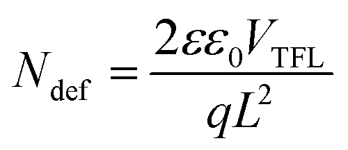 | (2) |
 | ||
| Fig. 6 (a) Steady state photoluminescence, (b) dark J–V plots, (c) transient photovoltage (TPV), (d) transient photocurrent (TPC), (e) Mott–Schottky analysis, and (f) Nyquist plots of reference and OABr 0.1 mg mL−1 treated samples. | ||
TPV and TPC measurements of PSCs were obtained as shown in Fig. 6c and d. The experimental data were fitted using a biexponential decay function to quantify the charge carrier dynamics in the PSCs treated with OABr. PSCs with OABr increased their TPV decay periods from 0.6 μs (pristine) to 1.4 μs, showing an enhanced charge carrier recombination lifetime and decreased charge carrier recombination. Furthermore, the TPC decay times of PSCs with OABr were 2.3 μs, and TPC decay durations of PSCs were longer than those of pristine PSCs (1.4 μs). These findings suggest that OABr treatment induces more effective charge transport and extraction.55–57
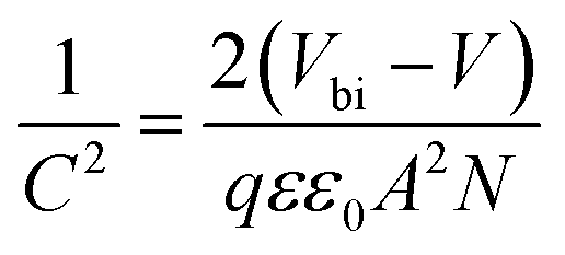
The built-in potentials (Vbi) of the two devices were further described using the Mott–Schottky analysis, as illustrated in Fig. 6e. The following equation describes the relationship between capacitance and DC voltage bias:
 | (3) |
To examine the impact of OABr on energy levels of perovskite, APS, Kelvin probe in the dark, and SPV measurements were carried out in order to reveal changes in valence band maximum, VBM, WF and Fermi level. The APS analysis shown in Fig. S10a and b† revealed a decrease in the VBM by 0.23 eV from −5.45 eV (reference) to −5.68 eV (OABr), which in practice, would favor the transport of charge carriers to the HTL due to an optimum energy level offset of about 0.28 eV between the VBM of the perovskite and the HOMO of PTAA.64,65 The XPS measurements of the VB region presented in Fig. S10c† show that the VBM is located at −1.2 eV below the Fermi level or at −5.4 eV with respect to the vacuum level, in excellent agreement with the APS measurements. However, a shift in the VBM was not detected for OABr, which can be explained by the lower resolution of XPS compared to that of APS in the VB region and/or the different information depths of the two techniques, i.e., APS is more surface sensitive. Kelvin-probe measurements were carried out in the dark to estimate the WF. The Kelvin probe measurements are presented in Fig. S11† and the WF values are summarized in Table S3.† Clearly, a significant increase in the WF is observed as the percentage of OABr increases, up to +0.6 eV for OABr 0.1 mg mL−1. The increase in the WF is associated with an interface dipole induced at the surface of the OABr molecules and not with a weak p-type transformation of the perovskite. The alignment of the energy level in the device is sketched in Fig. 7 and shows a downward shift of the energy level of the perovskite after applying OABr at a concentration of 0.1 mg mL−1 in the antisolvent solution. The conduction band minimum, CBM, of the perovskite was reduced, causing a “spike” configuration at the perovskite/PC61BM interface of approximately 0.14 eV. A “spike” configuration has been shown to reduce interface recombination and to increase the PCE.66–68 We have shown in our previous work that a “spike” configuration at the perovskite/ETL interface is beneficial for the performance of inverted PSCs.69
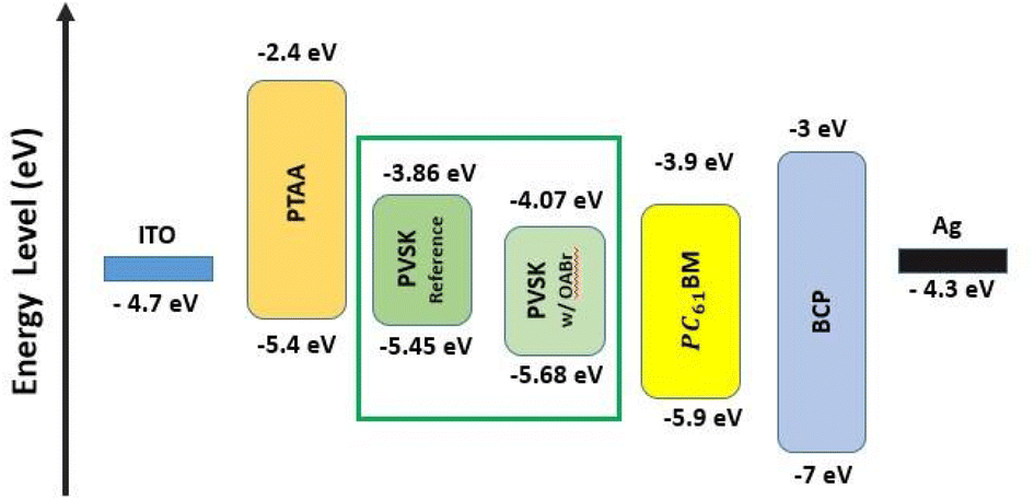 | ||
| Fig. 7 Energy level alignment in the device layer stack. | ||
Fig. S12† shows the normalized SPV spectra of perovskite films treated with OABr and compared with that of the reference. The samples were kept in the dark and then illuminated with white light, causing an SPV response. The difference in surface potential between the light and dark states was used to characterize the perovskite layer's carrier separation capabilities.70,71 The perovskite film treated with an optimal OABr concentration exhibited the highest SPV difference with respect to the reference, which correlates with the higher Voc of the corresponding devices.34 Moreover, after the light was turned off, the SPV decayed to its initial value. The SPV decay was fitted to a simple exponential function as discussed in the ESI.† The decay rate parameter decreases as the OABr concentration increases in the antisolvent solution, indicating that the total density of traps in the perovskite film was reduced with the OABr treatment.72
3.4 Stability measurements
The stability of the reference and OABr treated PSCs was examined under diverse environmental circumstances. Fig. 8a shows successive optical images of perovskite films treated with OABr compared to the reference, aged at room temperature and 60% relative humidity (RH). The reference perovskite film exhibited poor humidity stability and rapidly degraded after 24 hours to the yellow PbI2 phase. In contrast, the OABr modified films showed better stability, even for a lower OABr concentration of 0.01 mg mL−1, and the stability of the perovskite increased with higher amounts of OABr in the antisolvent. The perovskite films treated with an OABr concentration greater than 0.1 mg mL−1 remained almost unaffected by humidity after 4 days of exposure, as shown in Fig. 8a (the arrow represents the evolution of time). This experiment reveals the improvement in humidity stability of the perovskite film, which can be attributed to the better quality of the perovskite film and the bigger perovskite grains. The grain boundaries are susceptible to humidity, and it has been shown that the humidity degradation starts from there.73 The increase in grain size with OABr treatment reduces the grain boundaries and enhances the stability of the perovskite to humidity. It is not surprising that the 0.25 mg mL−1 OABr treated perovskite film, which exhibits the largest perovskite grains and indistinguishable grain boundaries, also exhibits the highest stability under humidity. Moreover, the OABr located on the surface of the perovskite could impede water penetration and protect the perovskite from degradation.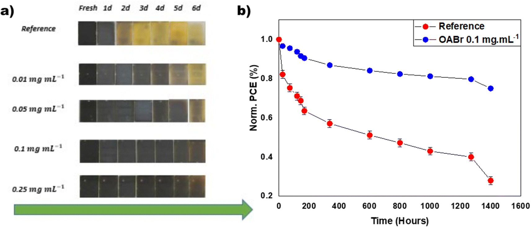 | ||
| Fig. 8 (a) Photographs of perovskite samples that age under ambient conditions with a relative humidity of 65% and a temperature of 25 °C. (b) Long term stability measurements of encapsulated perovskite devices under continuous 1 sun illumination, at 65 °C and 10–15% RH. The normalized PCE of the control device (red points) is compared with that of the optimal OABr treated sample (0.1 mg mL−1) device (blue points). | ||
The long-term operational stability of the PSCs is also an important performance metric for the commercial future of this technology. PSCs degrade when exposed to humidity, thermal stress, and UV light, limiting their lifetime.74–76 The long-term stability of the PSCs was evaluated following the ISOS-L2 protocol, i.e., the samples were tested under continuous 1 sun illumination at temperatures exceeding 65 °C.77 In panel b of Fig. 8, the long-term stability behavior of the reference device is compared to that of the optimal 0.1 mg mL−1 OABr device. After 1400 hours, the OABr treated device retains almost 80% of the initial PCE, while the reference device retains only 25%. The improved stability of OABr treated devices is ascribed to the improved crystallinity and larger grain size of the perovskite film, which prevent perovskite degradation.78,79
4. Discussion
The thin film characterization revealed that adding OABr to the antisolvent mixture alters the nucleation rate and the crystal growth of the perovskite. The XRD measurements indicated the improved crystallinity of the OABr treated sample and the preferential orientation of the perovskite crystal domains toward the (100) direction. Interestingly, OABr treatment induced compressive deformation in the perovskite lattice. This conclusion is additionally supported by the AFM images, which show a wave like pattern that can be associated with compressive strain in the horizontal direction with the OABr treatment. The compressive strain in the perovskite film is beneficial for the stability of the devices and for reducing defects and non-radiative recombination, according to previous reports.80–82 The morphological characterization through SEM and AFM shows that the grain size increases exponentially with the OABr concentration. Therefore, the grain boundaries that are sites for non-radiative recombination decrease with OABr treatment. According to XPS and APS analysis, the OABr molecules are concentrated on the surface of the perovskite, and their dipole moment points toward the substrate. Thus, the WF increases with the OABr concentration to 4.8 eV. The alkylammonium salts exhibit dipole moments in the range of 5–11 Debye83–85 and thus can easily induce a WF increase of +0.6 eV.In addition to morphological changes, the band gap of the perovskite increases by 0.02 eV for the 0.1 mg mL−1 OABr sample. The increase in the band gap probably is not related to the induced compressive strain in the film, because previous studies have shown that compressive strain tends to decrease the band gap.86,87 However, according to a recent theoretical study, a low compressive strain may decrease the band gap, but a high compressive strain could increase the band gap.88 The increase in the band gap may relate to Br− ion exchange, resulting in a bromide-rich perovskite, or to the formation of 2D perovskite phases near the surface of the perovskite. The former is not likely, since the XPS analysis indicated that the Br− ions of the OABr salt are mostly located on the surface. Previous studies have shown the formation of 2D/3D phases with the application of OABr and other octylammonium salts over the perovskite as a surface treatment layer21,32 and therefore the formation of 2D/3D phases is very possible in our OABr treated samples, but we did not find experimental evidence to support this. Hence, with the addition of OABr in the antisolvent mixture we achieve the enhancement of the crystallinity and an increase in the grain size, and possibly the simultaneous formation of 2D/3D perovskite phases near the perovskite surface, which further passivate the perovskite surface, reducing the surface recombination at the interfaces with the CTLs.
A change in the band gap of the perovskite will affect the photovoltaic parameters according to the Shockley–Queisser (SQ) balance limit.89 Consequently, the maximum achievable photovoltaic parameters were acquired from the work of S. Rühle90 using the band gap values estimated from the inflection point of the EQE. Table S4† presents the theoretical SQ photovoltaic parameters compared to the experimental ones. As shown in Table S4,† an increase in the band gap of 0.02 eV should have decreased Jsc to approximately 2.8%, but the experimental Jsc only decreased by 0.7%, indicating that the better crystallization of the perovskite and the reduction of non-radiative recombination limited the reduction in Jsc. In addition, the improved PTAA/perovskite interface increased the light absorption, as also shown from the EQE. The Voc was expected to increase by 1.4% but the Voc was increased by 11.8%. Similarly, the FF increased more than the expected theoretical one. PCE was expected to decrease by about 1.3% but instead we observed an increase by 12.2%. Therefore, the observed improvement in Voc and the FF upon treatment with OABr is not attributed to the increase in Eg,pv of the perovskite, but to the enhanced crystallinity of the perovskite and the reduction of non-radiative recombination.
To estimate the voltage losses due to non-radiative recombination, we adopted the method described in the work of L. Krückemeier et al.91 This method requires the EQE spectra as the input and an assumption of Urbach energy. For our calculations we assumed a typical Urbach energy of 16 meV. The voltage loss due to non-radiative recombination ΔVnradoc was estimated at 0.282 V for the reference device and at 0.159 V for the best performing OABr device; that is, the non-radiative losses are almost halved (43.6% reduction). The total Voc losses, ΔV, considering non-radiative recombination, sub-gap radiative recombination and radiative recombination above the band gap, were estimated at 567 mV for the reference and 450 mV for the optimized OABr devices. More information on the estimation of the ΔV losses is provided in the ESI.†Fig. 9a visualizes the Voc losses and highlights the improvement induced by the OABr treatment. The higher band gap of the perovskite treated with OABr results in slightly higher radiative recombination and thermodynamic loss (about 6 mV more than that of the reference). However, the non-radiative recombination is considerably suppressed. The steady-state and transient analyses proved that the OABr treatment improved the perovskite film quality, significantly lowered the trap density, and suppressed non-radiative recombination, ultimately resulting in a higher Voc and PCE. In Fig. S13 and Table S6† we compare the non-radiative losses of our optimized device with those of the current best performing inverted devices with similar structures i.e., inverted PSCs with only solution processed layers. Electron transport layers evaporated on the perovskite were excluded from the comparison. Our optimized devices, that feature undoped CTLs and no additional passivation layers, exhibit very low non-radiative losses and are ranked close to the best performing devices that employ 2D perovskite and/or passivation layers over/below the perovskite layer.
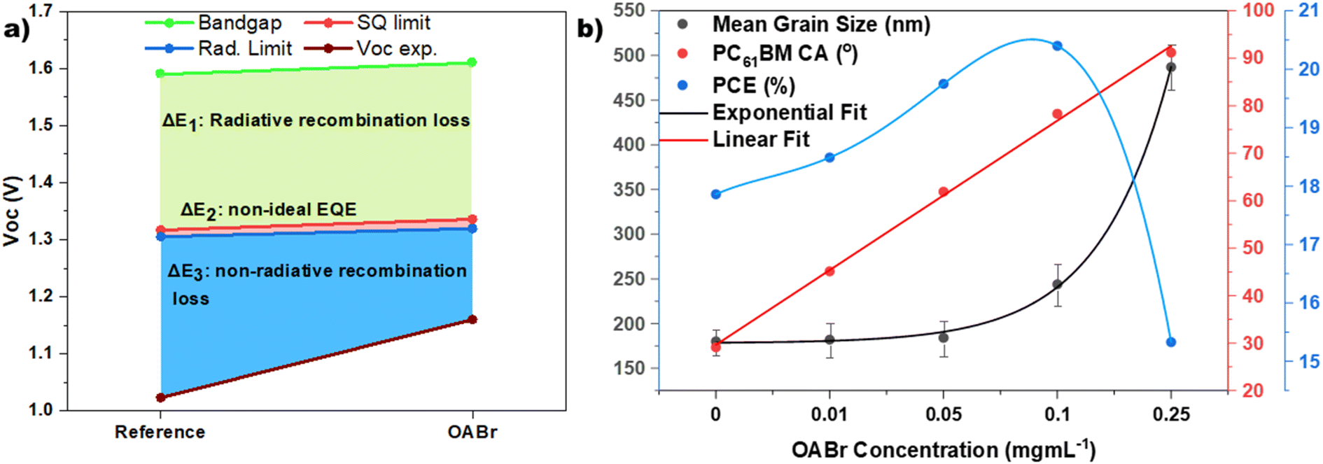 | ||
| Fig. 9 (a) Analysis of Voc loss of the reference and optimized OABr treated devices. The OABr PSCs exhibit significant suppression of the non-radiative recombination. (b) The mean grain size (in nm, left axis), the PC61BM contact angle (CA in degrees, right inner axis), and PCE (in %, right outer axis) are plotted versus the concentration of OABr in the antisolvent. | ||
Despite the excellent improvement in PCE as OABr increases, PCE drops sharply when OABr increases to 0.25 mg mL−1 (Fig. 2). In Fig. 9b the size of the perovskite grains, the contact angle of the PC61BM droplet on the perovskite surface, and the PCE as a function of the OABr mg mL−1 concentration in the antisolvent solution are plotted. Interestingly, the grain size increases exponentially with the OABr concentration, while the contact angle increases linearly. As expected, PCE follows the grain size trend and increases as the OABr concentration increases. However, OABr concentrations greater than 0.1 mg mL−1 resulted in a lower PCE. This is related to the high contact angle, which indicates that severe dewetting of PC61BM occurred and that PC61BM was unable to fully cover the surface of the perovskite. This fact leaves more room for future research with the aim of improving the wetting of PC61BM on the perovskite with the largest grains. Furthermore, OABr was deposited on the perovskite layer through spin coating OABr solutions of 1 and 2 mg mL−1, in order to form a thin passivating film on the perovskite in accordance with the most common approach to passivation of perovskite in the literature. Fig. S14a† shows contact images of a PC61BM droplet on the perovskite layer treated with spin coated OABr. The droplet forms a high contact angle of about 90°, similar to the perovskite layer treated with a high concentration of OABr in the antisolvent, and this can lead to PC61BM dewetting. Devices implementing OABr as a passivation layer were fabricated and the JV curves are shown in Fig. S14b† along with the photovoltaic parameters in Table S7.† As expected, the devices showed low PCE due to poor PC61BM formation. Therefore, a high concentration of OA+ cations on the perovskite surface causes challenges for the growth of a good PC61BM layer, and the common approach of depositing an OABr layer on the perovskite with spin coating is inadequate for inverted PSCs. The proposed approach of using OABr in antisolvent eliminates this problem, exploiting the passivation properties of OABr without affecting the growth of PC61BM.
5. Conclusions
In conclusion, we developed a simple way to produce efficient and stable PSCs by introducing the organic salt OABr in the antisolvent step. The proposed engineering approach is a novel strain-regulating approach to induce a compressive strain in the perovskite film and to improve film properties. This approach enables the fabrication of a high quality perovskite film demonstrating multiple functionalities, including increased crystallization of the perovskite film, larger perovskite grains, reduced trap density, suppressed non-radiative recombination, improved charge extraction, and better humidity stability. An optimal concentration of 0.1 mg mL−1 of OABr in the antisolvent mixture resulted in reducing the non-radiative losses by 43.6%, allowing 137 mV to be recovered; thus the devices exhibited a Voc of 1.16 V and a PCE of 20.4%. It was also shown that the OABr treatment drastically reduced the degradation rate of the perovskite layer under humid conditions and the OABr enabled devices exhibited long-term stability retaining 80% of the initial PCE for 1400 h under the ISOS-L2 protocol. Our proposed engineering approach, without adding an additional manufacturing step, provides a straightforward method for enhancing both the stability and the efficiency of inverted PSCs, which can be further improved by optimizing the PC61BM deposition.Conflicts of interest
There are no conflicts of interest to declare.Acknowledgements
This work was funded by the Greece-China joint R&D project Calypso (T7ΔKI-00039), co-financed by Greece, the EU Regional Development Fund and the Chinese Ministry of Science and Technology. The authors would also like to acknowledge Alexanda Manousaki from the University of Crete, Physics Department, Heraklion, Crete, (Greece), for SEM-EDS characterization.References
- J. Jeong, M. Kim, J. Seo, H. Lu, P. Ahlawat, A. Mishra, Y. Yang, M. A. Hope, F. T. Eickemeyer, M. Kim, Y. J. Yoon, I. W. Choi, B. P. Darwich, S. J. Choi, Y. Jo, J. H. Lee, B. Walker, S. M. Zakeeruddin, L. Emsley, U. Rothlisberger, A. Hagfeldt, D. S. Kim, M. Grätzel and J. Y. Kim, Nature, 2021, 592, 381 CrossRef CAS PubMed.
- M. Kim, J. Jeong, H. Lu, T. K. Lee, F. T. Eickemeyer, Y. Liu, I. W. Choi, S. J. Choi, Y. Jo, H.-B. Kim, S.-I. Mo, Y.-K. Kim, H. Lee, N. G. An, S. Cho, W. R. Tress, S. M. Zakeeruddin, A. Hagfeldt, J. Y. Kim, M. Grätzel and D. S. Kim, Science, 2022, 375, 302 CrossRef CAS PubMed.
- H. S. Jung and N. G. Park, Small, 2015, 11, 10 CrossRef CAS PubMed.
- P. Docampo and T. Bein, Acc. Chem. Res., 2016, 49, 339 CrossRef CAS.
- Q. Liu, Y. Jiang, K. Jin, J. Qin, J. Xu, W. Li, J. Xiong, J. Liu, Z. Xiao, K. Sun, S. Yang, X. Zhang and L. Ding, Sci. Bull., 2020, 65, 272 CrossRef CAS.
- N. E. Courtier, J. M. Cave, J. M. Foster, A. B. Walker and G. Richardson, Energy Environ. Sci., 2019, 12, 396 RSC.
- N. Tzoganakis, D. Tsikritzis, K. Chatzimanolis, X. Zhuang and E. Kymakis, Nanomaterials, 2023, 13, 883 CrossRef CAS PubMed.
- K. X. Steirer, P. Schulz, G. Teeter, V. Stevanovic, M. Yang, K. Zhu and J. J. Berry, ACS Energy Lett., 2016, 1, 360 CrossRef CAS.
- R. Brenes, D. Guo, A. Osherov, N. K. Noel, C. Eames, E. M. Hutter, S. K. Pathak, F. Niroui, R. H. Friend, M. S. Islam, H. J. Snaith, V. Bulović, T. J. Savenije and S. D. Stranks, Joule, 2017, 1, 155 CrossRef CAS.
- P. Schulz, D. Cahen and A. Kahn, Chem. Rev., 2019, 119, 3349 CrossRef CAS PubMed.
- Q. Cao, Y. Li, H. Zhang, J. Yang, J. Han, T. Xu, S. Wang, Z. Wang, B. Gao, J. Zhao, X. Li, X. Ma, S. M. Zakeeruddin, W. E. I. Sha, X. Li and M. Grätzel, Sci. Adv., 2021, 7, eabg0633 CrossRef CAS PubMed.
- Q. Jiang, Y. Zhao, X. Zhang, X. Yang, Y. Chen, Z. Chu, Q. Ye, X. Li, Z. Yin and J. You, Nat. Photonics, 2019, 13, 460 CrossRef CAS.
- D. Tsikritzis, K. Rogdakis, K. Chatzimanolis, M. Petrović, N. Tzoganakis, L. Najafi, B. Martín-García, R. Oropesa-Nuñez, S. Bellani, A. E. Del Rio Castillo, M. Prato, M. M. Stylianakis, F. Bonaccorso and E. Kymakis, Mater. Adv., 2020, 1, 450 RSC.
- K. Chatzimanolis, K. Rogdakis, D. Tsikritzis, N. Tzoganakis, M. Tountas, M. Krassas, S. Bellani, L. Najafi, B. Martín-García, R. Oropesa-Nuñez, M. Prato, G. Bianca, I. Plutnarova, Z. Sofer, F. Bonaccorso and E. Kymakis, Nanoscale Adv., 2021, 3, 3124 RSC.
- P. Liu, N. Han, W. Wang, R. Ran, W. Zhou and Z. Shao, Adv. Mater., 2021, 33, 2002582 CrossRef CAS PubMed.
- H. Tsai, W. Nie, J. C. Blancon, C. C. Stoumpos, R. Asadpour, B. Harutyunyan, A. J. Neukirch, R. Verduzco, J. J. Crochet, S. Tretiak, L. Pedesseau, J. Even, M. A. Alam, G. Gupta, J. Lou, P. M. Ajayan, M. J. Bedzyk, M. G. Kanatzidis and A. D. Mohite, Nature, 2016, 536, 312 CrossRef CAS PubMed.
- C. Liang, D. Zhao, Y. Li, X. Li, S. Peng, G. Shao and G. Xing, Energy Environ. Mater., 2018, 1, 221 CrossRef CAS.
- S. Wang, F. Cao, Y. Wu, X. Zhang, J. Zou, Z. Lan, W. Sun, J. Wu and P. Gao, Mater. Today Phys., 2021, 21, 100543 CrossRef CAS.
- W. Shi and H. Ye, J. Phys. Chem. Lett., 2021, 12, 4052 CrossRef CAS PubMed.
- P. Chen, Y. Bai, S. Wang, M. Lyu, J. H. Yun and L. Wang, Adv. Funct. Mater., 2018, 28, 1706923 CrossRef.
- N. Mozaffari, T. Duong, M. M. Shehata, A. D. Bui, H. T. Pham, Y. Yin, Y. O. Mayon, J. Zheng, M. A. Mahmud, G. D. Tabi, G. G. Andersson, L. E. Black, J. Peng, H. Shen, T. P. White, K. Weber and K. R. Catchpole, Sol. RRL, 2022, 6, 2200355 CrossRef CAS.
- S. Rahmany and L. Etgar, Mater. Adv., 2021, 2, 2617 RSC.
- J. J. Yoo, S. Wieghold, M. C. Sponseller, M. R. Chua, S. N. Bertram, N. T. P. Hartono, J. S. Tresback, E. C. Hansen, J.-P. Correa-Baena, V. Bulović, T. Buonassisi, S. S. Shin and M. G. Bawendi, Energy Environ. Sci., 2019, 12, 2192 RSC.
- A. Krishna, S. Gottis, M. K. Nazeeruddin and F. Sauvage, Adv. Funct. Mater., 2019, 29, 1806482 CrossRef.
- J. Xue, R. Wang, K. L. Wang, Z. K. Wang, I. Yavuz, Y. Wang, Y. Yang, X. Gao, T. Huang, S. Nuryyeva, J. W. Lee, Y. Duan, L. S. Liao, R. Kaner and Y. Yang, J. Am. Chem. Soc., 2019, 141, 13948 CrossRef CAS PubMed.
- L. Fu, H. Li, L. Wang, R. Yin, B. Li and L. Yin, Energy Environ. Sci., 2020, 13, 4017 RSC.
- H. Kim, S. U. Lee, D. Y. Lee, M. J. Paik, H. Na, J. Lee and S. Il Seok, Adv. Energy Mater., 2019, 9, 1902740 CrossRef CAS.
- S. Gharibzadeh, B. Abdollahi Nejand, M. Jakoby, T. Abzieher, D. Hauschild, S. Moghadamzadeh, J. A. Schwenzer, P. Brenner, R. Schmager, A. A. Haghighirad, L. Weinhardt, U. Lemmer, B. S. Richards, I. A. Howard and U. W. Paetzold, Adv. Energy Mater., 2019, 9, 1803699 CrossRef.
- T. M. Koh, V. Shanmugam, X. Guo, S. S. Lim, O. Filonik, E. M. Herzig, P. Müller-Buschbaum, V. Swamy, S. T. Chien, S. G. Mhaisalkar and N. Mathews, J. Mater. Chem. A, 2018, 6, 2122 RSC.
- S. Tan, I. Yavuz, M. H. Weber, T. Huang, C. H. Chen, R. Wang, H. C. Wang, J. H. Ko, S. Nuryyeva, J. Xue, Y. Zhao, K. H. Wei, J. W. Lee and Y. Yang, Joule, 2020, 4, 2426 CrossRef CAS.
- M. Jeong, I. W. Choi, E. M. Go, Y. Cho, M. Kim, B. Lee, S. Jeong, Y. Jo, H. W. Choi, J. Lee, J. H. Bae, S. K. Kwak, D. S. Kim and C. Yang, Science, 2020, 369, 1615 CrossRef CAS PubMed.
- M. A. Mahmud, H. T. Pham, T. Duong, Y. Yin, J. Peng, Y. Wu, W. Liang, L. Li, A. Kumar, H. Shen, D. Walter, H. T. Nguyen, N. Mozaffari, G. D. Tabi, G. Andersson, K. R. Catchpole, K. J. Weber and T. P. White, Adv. Funct. Mater., 2021, 31, 2104251 CrossRef CAS.
- C. A. R. Perini, E. Rojas-Gatjens, M. Ravello, A. F. Castro-Mendez, J. Hidalgo, Y. An, S. Kim, B. Lai, R. Li, C. Silva-Acuña and J. P. Correa-Baena, Adv. Mater., 2022, 34, 2204726 CrossRef CAS PubMed.
- J. J. Yoo, S. Wieghold, M. C. Sponseller, M. R. Chua, S. N. Bertram, N. T. P. Hartono, J. S. Tresback, E. C. Hansen, J. P. Correa-Baena, V. Bulović, T. Buonassisi, S. S. Shin and M. G. Bawendi, Energy Environ. Sci., 2019, 12, 2192 RSC.
- T. Duong, H. Pham, Y. Yin, J. Peng, M. A. Mahmud, Y. L. Wu, H. Shen, J. Zheng, T. Tran-Phu, T. Lu, L. Li, A. Kumar, G. G. Andersson, A. Ho-Baillie, Y. Liu, T. White, K. Weber and K. Catchpole, J. Mater. Chem. A, 2021, 9, 18454 RSC.
- S. Y. Kwon, B. Kang, J. H. Won, C. Y. Lee, K. Hwang, H. H. Kim, D. Park, W. K. Choi, I. S. Kim, G. Y. Kim, Y. H. Jang, P. Lee, S. H. Im and T. Kim, Adv. Mater. Interfaces, 2023, 10, 2202249 CrossRef CAS.
- J. Sun, F. Li, J. Yuan and W. Ma, Small Methods, 2021, 5, 2000744 CrossRef PubMed.
- D. Bi, C. Yi, J. Luo, J. D. Décoppet, F. Zhang, S. M. Zakeeruddin, X. Li, A. Hagfeldt and M. Grätzel, Nat. Energy, 2016, 1, 16142 CrossRef CAS.
- Y. Wu, X. Yang, W. Chen, Y. Yue, M. Cai, F. Xie, E. Bi, A. Islam and L. Han, Nat. Energy, 2016, 1, 16148 CrossRef CAS.
- Y. J. Kang, S. N. Kwon, S. P. Cho, Y. H. Seo, M. J. Choi, S. S. Kim and S. I. Na, ACS Energy Lett., 2020, 5, 2535 CrossRef CAS.
- T. S. Ripolles, P. Serafini, C. Redondo-Obispo, E. Climent-Pascual, S. Masi, I. Mora-Seró and C. Coya, Energy Technol., 2022, 10, 2100890 CrossRef CAS.
- Y. Huang, T. Liu, B. Wang, J. Li, D. Li, G. Wang, Q. Lian, A. Amini, S. Chen, C. Cheng and G. Xing, Adv. Mater., 2021, 33, 2102816 CrossRef CAS.
- M. Cha, P. Da, J. Wang, W. Wang, Z. Chen, F. Xiu, G. Zheng and Z. S. Wang, J. Am. Chem. Soc., 2016, 138, 8581 CrossRef CAS PubMed.
- X. Zheng, J. Troughton, N. Gasparini, Y. Lin, M. Wei, Y. Hou, J. Liu, K. Song, Z. Chen, C. Yang, B. Turedi, A. Y. Alsalloum, J. Pan, J. Chen, A. A. Zhumekenov, T. D. Anthopoulos, Y. Han, D. Baran, O. F. Mohammed, E. H. Sargent and O. M. Bakr, Joule, 2019, 3, 1963 CrossRef CAS.
- D. Ghosh, D. K. Chaudhary, M. Y. Ali, K. K. Chauhan, S. Prodhan, S. Bhattacharya, B. Ghosh, P. K. Datta, S. C. Ray and S. Bhattacharyya, Chem. Sci., 2019, 10, 9530 RSC.
- X. Li, W. Li, Y. Yang, X. Lai, Q. Su, D. Wu, G. Li, K. Wang, S. Chen, X. W. Sun and A. K. K. Kyaw, Sol. RRL, 2019, 3, 1900029 CrossRef.
- N. Tzoganakis, B. Feng, M. Loizos, M. Krassas, D. Tsikritzis, X. Zhuang and E. Kymakis, J. Mater. Chem. C, 2021, 9, 14709 RSC.
- N. Tzoganakis, B. Feng, M. Loizos, K. Chatzimanolis, M. Krassas, D. Tsikritzis, X. Zhuang and E. Kymakis, Energy Technol., 2023, 11, 2201017 CrossRef CAS.
- B. J. Kim, M. cheol Kim, D. G. Lee, G. Lee, G. J. Bang, J. B. Jeon, M. Choi and H. S. Jung, Adv. Mater. Interfaces, 2018, 5, 1800993 CrossRef.
- J. Haddad, B. Krogmeier, B. Klingebiel, L. Krückemeier, S. Melhem, Z. Liu, J. Hüpkes, S. Mathur and T. Kirchartz, Adv. Mater. Interfaces, 2020, 7, 2000366 CrossRef CAS.
- O. Almora, C. I. Cabrera, J. Garcia-Cerrillo, T. Kirchartz, U. Rau, C. J. Brabec, J. Garcia-Cerrillo, T. Kirchartz, U. Rau and C. J. Brabec, Adv. Energy Mater., 2021, 11, 2100022 CrossRef CAS.
- S. Bansal and P. Aryal, 2017 IEEE 44th Photovolt. Spec. Conf., PVSC, 2017, p. 3220 Search PubMed.
- G. Williamson and W. Hall, Acta Metall., 1953, 1, 22 CrossRef CAS.
- J. Rodriguez-Pereira, J. Tirado, A. F. Gualdrón-Reyes, F. Jaramillo and R. Ospina, Surf. Sci. Spectra, 2020, 27, 024003 CrossRef CAS.
- E. L. Unger, E. T. Hoke, C. D. Bailie, W. H. Nguyen, A. R. Bowring, T. Heumüller, M. G. Christoforo and M. D. McGehee, Energy Environ. Sci., 2014, 7, 3690 RSC.
- R. Hidayat, A. A. Nurunnizar, A. Fariz, Herman, E. S. Rosa, Shobih, T. Oizumi, A. Fujii and M. Ozaki, Sci. Rep., 2020, 10, 19197 CrossRef CAS PubMed.
- M. Daboczi, I. Hamilton, S. Xu, J. Luke, S. Limbu, J. Lee, M. A. McLachlan, K. Lee, J. R. Durrant, I. D. Baikie and J. S. Kim, ACS Appl. Mater. Interfaces, 2019, 11, 46808 CrossRef CAS.
- P. Liu, Z. Liu, C. Qin, T. He, B. Li, L. Ma, K. Shaheen, J. Yang, H. Yang, H. Liu, K. Liu and M. Yuan, Sol. Energy Mater. Sol. Cells, 2020, 212, 110555 CrossRef CAS.
- J. Yang, S. Xiong, J. Song, H. Wu, Y. Zeng, L. Lu, K. Shen, T. Hao, Z. Ma, F. Liu, C. Duan, M. Fahlman and Q. Bao, Adv. Energy Mater., 2020, 10, 200687 Search PubMed.
- O. Almora, C. Aranda, E. Mas-Marzá and G. Garcia-Belmonte, Appl. Phys. Lett., 2016, 109, 173903 CrossRef.
- S. M. Abdulrahim, Z. Ahmad, M. Q. Mehmood, S. Paek, J. Bhadra, N. J. Al-Thani, M. K. Nazeeruddin, A. Belaidi and M. Amani, J. Electroanal. Chem., 2021, 902, 115800 CrossRef CAS.
- Y. Feng, J. Bian, S. Wang, C. Zhang, M. Wang and Y. Shi, J. Mater. Chem. C, 2019, 7, 8294 RSC.
- D. Klotz, G. Tumen-Ulzii, C. Qin, T. Matsushima and C. Adachi, RSC Adv., 2019, 9, 33436 RSC.
- M. Stolterfoht, P. Caprioglio, C. M. Wolff, J. A. Márquez, J. Nordmann, S. Zhang, D. Rothhardt, U. Hörmann, Y. Amir, A. Redinger, L. Kegelmann, F. Zu, S. Albrecht, N. Koch, T. Kirchartz, M. Saliba, T. Unold and D. Neher, Energy Environ. Sci., 2019, 12, 2778 RSC.
- Z. Sun, Y. Kang, G. Wang, M. Liang and S. Xue, J. Phys. Chem. C, 2020, 124, 12912 CrossRef CAS.
- T. Minemoto, Y. Hashimoto, W. Shams-Kolahi, T. Satoh, T. Negami, H. Takakura and Y. Hamakawa, Sol. Energy Mater. Sol. Cells, 2003, 75, 121 CrossRef CAS.
- C. Ding, Y. Zhang, F. Liu, Y. Kitabatake, S. Hayase, T. Toyoda, K. Yoshino, T. Minemoto, K. Katayama and Q. Shen, Nano Energy, 2018, 53, 17 CrossRef CAS.
- G. Kapil, T. S. Ripolles, K. Hamada, Y. Ogomi, T. Bessho, T. Kinoshita, J. Chantana, K. Yoshino, Q. Shen, T. Toyoda, T. Minemoto, T. N. Murakami, H. Segawa and S. Hayase, Nano Lett., 2018, 18, 3600 CrossRef CAS PubMed.
- D. Tsikritzis, K. Chatzimanolis, N. Tzoganakis, S. Bellani, M. I. Zappia, G. Bianca, N. Curreli, J. Buha, I. Kriegel, N. Antonatos, Z. Sofer, M. Krassas, K. Rogdakis, F. Bonaccorso and E. Kymakis, Sustainable Energy Fuels, 2022, 6, 5345 RSC.
- X. Ling, J. Yuan, D. Liu, Y. Wang, Y. Zhang, S. Chen, H. Wu, F. Jin, F. Wu, G. Shi, X. Tang, J. Zheng, S. F. Liu, Z. Liu and W. Ma, ACS Appl. Mater. Interfaces, 2017, 9, 23181 CrossRef CAS.
- Q. Lou, Y. Han, C. Liu, K. Zheng, J. Zhang, X. Chen, Q. Du, C. Chen and Z. Ge, Adv. Energy Mater., 2021, 11, 2101416 CrossRef CAS.
- A. B. Walker, L. M. Peter, K. Lobato and P. J. Cameron, J. Phys. Chem. B, 2006, 110, 25504 CrossRef CAS PubMed.
- C. C. Boyd, R. Cheacharoen, T. Leijtens and M. D. McGehee, Chem. Rev., 2019, 119, 3418 CrossRef CAS.
- D. B. Khadka, Y. Shirai, M. Yanagida, K. Uto and K. Miyano, Sol. Energy Mater. Sol. Cells, 2022, 246, 111899 CrossRef CAS.
- Y. Wang, I. Ahmad, T. Leung, J. Lin, W. Chen, F. Liu, A. M. C. Ng, Y. Zhang and A. B. Djurišić, ACS Mater. Au, 2022, 3, 215–236 CrossRef.
- L. Duan and A. Uddin, Mater. Chem. Front., 2022, 6, 400 RSC.
- M. V Khenkin, E. A. Katz, A. Abate, G. Bardizza, J. J. Berry, C. Brabec, F. Brunetti, V. Bulović, Q. Burlingame, A. Di Carlo, R. Cheacharoen, Y.-B. Cheng, A. Colsmann, S. Cros, K. Domanski, M. Dusza, C. J. Fell, S. R. Forrest, Y. Galagan, D. Di Girolamo, M. Grätzel, A. Hagfeldt, E. von Hauff, H. Hoppe, J. Kettle, H. Köbler, M. S. Leite, S. Liu, Y.-L. Loo, J. M. Luther, C.-Q. Ma, M. Madsen, M. Manceau, M. Matheron, M. McGehee, R. Meitzner, M. K. Nazeeruddin, A. F. Nogueira, Ç. Odabaşı, A. Osherov, N.-G. Park, M. O. Reese, F. De Rossi, M. Saliba, U. S. Schubert, H. J. Snaith, S. D. Stranks, W. Tress, P. A. Troshin, V. Turkovic, S. Veenstra, I. Visoly-Fisher, A. Walsh, T. Watson, H. Xie, R. Yıldırım, S. M. Zakeeruddin, K. Zhu and M. Lira-Cantu, Nat. Energy, 2020, 5, 35 CrossRef.
- G. Tumen-Ulzii, C. Qin, D. Klotz, M. R. Leyden, P. Wang, M. Auffray, T. Fujihara, T. Matsushima, J. W. Lee, S. J. Lee, Y. Yang and C. Adachi, Adv. Mater., 2020, 32, 19205035 CrossRef PubMed.
- F. Fu, S. Pisoni, Q. Jeangros, J. Sastre-Pellicer, M. Kawecki, A. Paracchino, T. Moser, J. Werner, C. Andres, L. Duchêne, P. Fiala, M. Rawlence, S. Nicolay, C. Ballif, A. N. Tiwari and S. Buecheler, Energy Environ. Sci., 2019, 12, 3074 RSC.
- H. Zhang, Z. Chen, M. Qin, Z. Ren, K. Liu, J. Huang, D. Shen, Z. Wu, Y. Zhang, J. Hao, C. Lee, X. Lu, Z. Zheng, W. Yu and G. Li, Adv. Mater., 2021, 33, 2008487 CrossRef CAS.
- B. Yang, D. Bogachuk, J. Suo, L. Wagner, H. Kim, J. Lim, A. Hinsch, G. Boschloo, M. K. Nazeeruddin and A. Hagfeldt, Chem. Soc. Rev., 2022, 51, 7509 RSC.
- N. Rolston, K. A. Bush, A. D. Printz, A. Gold-Parker, Y. Ding, M. F. Toney, M. D. McGehee and R. H. Dauskardt, Adv. Energy Mater., 2018, 8, 1802139 CrossRef.
- O. Levy, G. Markovits and A. S. Kertes, J. Phys. Chem., 1971, 75, 542 CrossRef.
- I. P. Gol'dshtein, N. M. Alpatova, Y. M. Kessler, E. N. Gur’yanova and A. I. Gorbanev, Bull. Acad. Sci. USSR, Div. Chem. Sci., 1963, 12, 1543 CrossRef.
- N. M. Sinitsyn, T. M. Buslaeva, G. N. Kartsev, S. I. Ignat'eva and N. V. Egorova, Theor. Exp. Chem., 1978, 14, 301 CrossRef.
- C. Zhu, X. Niu, Y. Fu, N. Li, C. Hu, Y. Chen, X. He, G. Na, P. Liu, H. Zai, Y. Ge, Y. Lu, X. Ke, Y. Bai, S. Yang, P. Chen, Y. Li, M. Sui, L. Zhang, H. Zhou and Q. Chen, Nat. Commun., 2019, 10, 815 CrossRef CAS PubMed.
- D. Ghosh, A. Aziz, J. A. Dawson, A. B. Walker and M. S. Islam, Chem. Mater., 2019, 31, 4063 CrossRef CAS.
- L. Zhang, W. Geng, C. Tong, X. Chen, T. Cao and M. Chen, Sci. Rep., 2018, 8, 7760 CrossRef PubMed.
- W. Shockley and H. J. Queisser, J. Appl. Phys., 1961, 32, 510 CrossRef CAS.
- S. Rühle, Sol. Energy, 2016, 130, 139 CrossRef.
- L. Krückemeier, U. Rau, M. Stolterfoht and T. Kirchartz, Adv. Energy Mater., 2020, 10, 1902573 CrossRef.
Footnote |
| † Electronic supplementary information (ESI) available. See DOI: https://doi.org/10.1039/d3se00435j |
| This journal is © The Royal Society of Chemistry 2023 |