
 Open Access Article
 This Open Access Article is licensed under a Creative Commons Attribution-Non Commercial 3.0 Unported Licence
Porous silicon-nanowire-based electrode for the photoelectrocatalytic production of hydrogen†
Jingxian
Wang
ab,
Caroline
Keller
ac,
Marc
Dietrich
ad,
Paul E.
Olli
a,
Pascal
Gentile
d,
Stéphanie
Pouget
 e,
Hanako
Okuno
e,
Mohamed
Boutghatin
f,
Yan
Pennec
f,
Valérie
Reita
g,
Duc N.
Nguyen
bh,
Hannah
Johnson
i,
Adina
Morozan
b,
Vincent
Artero
*b and
Pascale
Chenevier
*a
e,
Hanako
Okuno
e,
Mohamed
Boutghatin
f,
Yan
Pennec
f,
Valérie
Reita
g,
Duc N.
Nguyen
bh,
Hannah
Johnson
i,
Adina
Morozan
b,
Vincent
Artero
*b and
Pascale
Chenevier
*a
aUniv. Grenoble Alpes, CEA, CNRS, IRIG, SyMMES, 38000 Grenoble, France. E-mail: pascale.chenevier@cea.fr
bUniv. Grenoble Alpes, CEA, CNRS, IRIG, Laboratoire de Chimie et Biologie des Métaux, 38000 Grenoble, France
cUniv. Grenoble Alpes, CEA, LITEN, DEHT, 38000 Grenoble, France
dUniv. Grenoble Alpes, CEA, Grenoble-INP, IRIG, PheLIQS, 38000 Grenoble, France
eUniv. Grenoble Alpes, CEA, IRIG, MEM, 38000 Grenoble, France
fUniv. Lille, CNRS, UMR 8520, IEMN – Institut d'Electronique de Microélectronique et de Nanotechnologie, Lille F-59000, France
gUniv. Grenoble Alpes, CNRS, Institut Néel, 38000 Grenoble, France
hUniversity of Science and Technology of Hanoi, Vietnam Academy of Science and Technology, Hanoi 100000, Vietnam
iToyota Motors Europe, Materials Engineering, Hoge Wei 33, 1930 Zaventem, Belgium
First published on 23rd August 2023
Abstract
Photoelectrochemical water splitting is a sustainable and environmentally friendly way to produce green hydrogen, for which the practical fabrication of low-cost photoelectrodes remains a challenge. Here we report a porous photocathode assembly based on silicon nanowires (SiNW) as a light absorber and non-precious molybdenum sulfide (MoSx) as a hydrogen-evolution catalyst. Tuning the SiNW diameter is key to select the light absorption wavelength range of the system. We demonstrate a facile and robust route to synthesize SiNWs with a controlled diameter from 13 to 48 nm directly on a porous conductive support. The high quality and homogeneity of the SiNWs grown by this method also allowed drawing unprecedented conclusions on the growth process, hinting towards a silylene path. Photocathodes baring SiNWs covered with MoSx perform photoelectrocatalytic production of hydrogen for several hours with a faradaic yield over 98%.
Introduction
Solar-driven water splitting in photoelectrochemical (PEC) cells has gained extensive attention recently to produce green hydrogen with minimal overall greenhouse gas emission.1 PEC cells are based on either a single light absorber or dual light absorbers. The dual absorber system consists of a photocathode for hydrogen evolution and a photoanode for oxygen evolution. With an optimal energetic alignment of the two photoelectrodes, a sufficient overall photovoltage (>1.23 V) can be obtained to dissociate water to H2 and O2.2 Based on the design of polymer electrolyte membrane (PEM) electrolyzers, gas-phase PEM-PEC cells have recently emerged as a scalable design for green hydrogen production.3 This device improves ion conductivity and allows the creation of higher surface area photoelectrodes.4,5Silicon is a promising light-harvesting material for photocathode because of its low cost, and suitable band gap and valence band potential towards the hydrogen evolution reaction (HER).6 Nanostructured Si, like silicon nanowires (SiNWs), attracts great interest for incorporation in PEC cell, as SiNWs have both long optical paths for efficient light absorption and short charge transport distance to the catalyst, which ensures the collection of the photogenerated charge carriers before they recombine.7–10 In addition, adjusting the SiNW diameter allows to tune the band gap,11 and thus the part of sun-light that will be absorbed. To date, SiNW production follows either a top-down approach, like metal assisted catalytic etching (MACE), or a bottom-up approach, like chemical vapour deposition (CVD) and solution growth.12 In MACE, an HF solution dissolves bulk Si at selected area where the Si surface is not masked by metal particles, leading to the formation of SiNW arrays on planar Si9,13,14 or Si powder.15 This method yields SiNWs at low temperature (50 °C) but provides SiNWs only on a Si wafer substrate, and gives better results on flat surfaces.16 CVD and solution growth based on Si crystallization from a silicon precursor are more versatile synthesis methods, as they allow the growth of SiNWs on different materials and support geometries.17 In CVD, a gas precursor, most often SiH4, decomposes at high temperature onto metal droplets in which the Si atom dissolves, and silicon crystallization18 follows at saturation. The surface of SiH4-fed CVD grown SiNWs is however a hydride Si![[thin space (1/6-em)]](https://www.rsc.org/images/entities/char_2009.gif) :H surface, reactive to air and humidity, which cannot be avoided during PEC cell operation. An alternative growth process involves organosilanes19 as silicon source in a vapor20,21 or supercritical22 phase, in which the SiNW surface is passivated by an organic shell from the organosilane.23,24
:H surface, reactive to air and humidity, which cannot be avoided during PEC cell operation. An alternative growth process involves organosilanes19 as silicon source in a vapor20,21 or supercritical22 phase, in which the SiNW surface is passivated by an organic shell from the organosilane.23,24
It is known that PEC hydrogen production at Si/electrolyte interfaces has a slow kinetics,7 therefore the silicon light-harvester has to be supplemented with a HER electrocatalyst. Platinum has been used extensively as catalyst in photoelectrochemical HER systems attaining up to 13% solar conversion efficiency.2 However, its scarcity and high cost limit its large-scale utilization. To compensate for their lower current density, PEC cells will include membrane-electrode-assembly of larger area than electrolyzers, thus consuming a larger amount of platinum for the same production of hydrogen. In this regard, noble-metal free HER catalysts are of particular interest. Molybdenum sulfide already demonstrated high catalytic activity, nontoxicity and chemical stability.25 Hu et al. reported that amorphous molybdenum sulfide (a-MoSx) prepared by electrodeposition from a MoS42− solution is compatible with a wide range of pH (pH = 0 to 13) with a significant geometric current density at low overpotential (15 mA cm−2 at η = 200 mV).26 Tran et al. pointed out that a-MoSx has a [Mo3S13]2− cluster-based polymeric structure and that eliminating terminal disulfide (S22−) ligands generates unsaturated Mo sites for H2 evolution.27 Recently, many methods have been developed to integrate molybdenum sulfides onto SiNWs and prepare photocathodes for H2 evolution, e.g. electrodeposition,28 photo-assisted electrodeposition,13 CVD (direct29 or indirect30), drop-casting,31,32 spin-coating.33 However, the efficient deposition of the a-MoSx catalyst on SiNWs within a porous electrode remains a challenge.
The present paper addresses the issue of building a noble-metal free, porous HER photoelectrode compatible with zero-gap PEM-PEC cells. A robust and tunable solvent-free technique is developed to grow SiNWs on a porous conductive substrate (PCS). The PEC performance of such porous photocathode is evaluated after electrodepositing a-MoSx on SiNWs as HER catalyst. A careful control of SiNW diameter from 13 to 48 nm allows maximizing the photocurrent at diameter 48 nm.
Material and methods
Materials
Gold(III) chloride hydrate (HAuCl4·3H2O, ∼50% Au basis), sodium citrate (99%), ascorbic acid, tetraoctylammonium bromide (TOAB, 98%), sodium borohydride (NaBH4, 99%) and ammonium tetrathiomolybdate ([MoS4](NH4)2, 99.97%) were purchased from Sigma Aldrich. Dodecanethiol (98%) was purchased from Alfa Aesar. Diphenylsilane (Ph2SiH2) was purchased from Chemical Point. The porous conductive support, a carbon paper designed as a gas diffusion layer without microporous layer (Sigracet 39 AA), was purchased from FuelCellStore.Gold nanoparticle synthesis
Gold nanoparticles (AuNPs), as a catalyst for SiNW growth, were synthesized by different methods in order to tune their size.34 The smallest AuNPs were synthesized using the Brust–Schiffrin method.35 Briefly, HAuCl4·3H2O was dissolved in water (12.5 mL, 41 mg mL−1). Toluene (120 mL) was added to the resulting solution along with TOAB (3.5 g) and dodecanethiol (0.6 mL). Then the organic phase was separated and reduced with NaBH4 aqueous solution (7.5 mL, 64 mg mL−1) at room temperature for 6 hours. AuNPs of 1–3 nm were dispersed in 20 mL chloroform after evaporation of toluene and purification by ethanol. The AuNPs from 12 to 50 nm were synthesized using the Turkevich method36 by mixing HAuCl4·3H2O aqueous solution with a sodium citrate solution at 100 °C for 5 minutes. The molar ratio of sodium citrate to HAuCl4 (Ct/Au) was the key factor to control the particle size. By decreasing the molar ratio from Ct/Au = 5.4, to 2.3 and then to 1.4, AuNP average size increased to 12 nm, 30 nm and 40 nm. The sample was let to cool down to room temperature and stored in a dry and clean bottle at 4 °C. The AuNPs of 80 nm were grown from smaller AuNPs according to the Ziegler and Eychmüller method.37 Briefly, HAuCl4·3H2O aqueous solution (60 mL, 3.3 mg mL−1) and the aqueous mixture (60 mL) of sodium citrate (4.1 mg mL−1) and ascorbic acid (2.1 mg mL−1) were slowly added to a seed solution with 12 nm AuNPs (11.5 mg L−1, 0.12 L) whilst stirring, and heated at 92 °C for 1 hour. The AuNPs in water were recovered after cooling down the solution to room temperature and stored in a dry and clean bottle at 4 °C.Silicon nanowire synthesis
SiNWs were grown in a 65 cm3 home-built stainless-steel reactor.24 AuNPs dispersed in water were transferred in an organic solvent, either toluene or ethanol, and drop-cast on a porous carbon substrate. AuNPs were drop-casted on the PCS in controlled amounts from 0.005 to 0.5 mg cm−2 (the area in this paper is meant as the PCS geometric area). The AuNP-loaded PCS placed in alumina crucibles were sealed in the reactor with 6 mL diphenylsilane under vacuum and heated at 430 °C from 1 to 6 h. After cooling down to room temperature, the reactor was carefully opened and the resulting PCS-SiNW were washed with dichloromethane and acetone and dried at 80 °C. For GC-MS analysis, the sub-products were collected by washing the reactor walls with dichloromethane.Electrodeposition of amorphous molybdenum sulfide
a-MoSx thin films were deposited by holding PCS-SiNW at anodic potential of 0.1 or 0.2 V versus the normal hydrogen electrode (NHE), in a deposition bath consisting of 1.0 mM [MoS4](NH4)2 in 1 M pH 7 phosphate buffer. The total density of charges was controlled at desired amount, which passed through the working electrode (1.6 cm2). After the electrodeposition of a-MoSx, the resulting PCS-SiNW-MoSx electrode was thoroughly washed with water and ethanol and dried in air at room temperature. In a control experiment, the same deposition was realized on PCS without SiNWs, yielding PCS-MoSx.Characterization
Scanning Electron Microscopy (SEM) (Zeiss Ultra55) was applied to characterize the nanowire morphology at an acceleration voltage of 5 kV and working distance of 5 mm. A JEOL 3010 high resolution transmission electron microscope operated at 300 kV was used to observe AuNPs. The samples for Transmission Electron Microscopy (TEM) were prepared by the ultrasonication of AuNPs in ethanol. Both the size of AuNPs and the diameter of SiNWs were measured using ImageJ software. Scanning Transmission Electron Microscopy (STEM) measurements were performed using a Cs-corrected Titan Themis (Thermofisher) at 200 kV. High Angle Annular Dark Field (HAADF) images were acquired with a convergence semi-angle of 20 mrad and collecting scattering from 55 mrad. Energy dispersive X-ray spectroscopy (EDX) was performed for elemental mapping using a Bruker EDX system consisting of four silicon drift detector in the Themis microscope. Electron energy loss spectroscopy (EELS) measurements were performed using a Gatan Quantum energy filter equipped with Dual EELS. For absorption spectroscopy, the SiNWs scratched with a blade from the surface of PCS-SiNW (0.25 cm2) were suspended in 2 mL dichloromethane in an ultrasound bath (10 min). The suspension was let to settle for 1 min, then the supernatant was placed in a 2 mm quartz cuvette for spectrophotometry. Powder X-ray diffraction has been carried out on a Panalytical X'Pert powder diffractometer equipped with a copper anode (λKα1 = 1.5406 Å, λKα2 = 1.5444 Å) and an X'Celerator 1D detector. It was configured in Bragg–Brentano geometry, with a variable divergence slit on the primary beam path and a set of antiscattering slits positioned before and after the sample. Axial divergence was limited by 0.02 rad Soller slits. Data analysis were performed using the Panalytical Highscore software. Raman spectra were collected on a WITec alpha 500 spectrometer, collecting the elastically scattered light (resolution < 0.9 cm−1) filtered by an edge filter from the ×100 objective of a confocal microscope, under the excitation of a laser of wavelength 532 nm. The laser intensity was maintained at a low power of 100 μW to avoid SiNW heating.23 Gas chromatography (GC) followed by mass spectroscopy (GC-MS) analyses were performed on a PerkinElmer Clarus 580 instrument using an optima 17 column with a FID detector and a Mass Spectrometer (MS) PerkinElmer Clarus SQ8S. GC-MS analyses were performed with the following temperature program: 65 °C for 3 minutes and a ramp of 16 °C per minute until 200 °C for a total time of 20 minutes. Products were identified by comparison with the same analyses of pure compounds and with referenced MS traces from the NIST database of organic molecules. In the photoelectrochemical tests, the produced gas evolution was regularly analyzed with a PerkinElmer Clarus 580 gas chromatograph equipped with a molecular sieve 5 Å column (30 m to 0.53 mm). The gas chromatograph was set-up in the so-called point injection flow mode. Samples of 50 μl from the headspace of the glass chamber used for the photoelectrochemical measurements, taken with a gas-tight syringe at defined times, were injected into the gas chromatograph. The area under the measured H2 peaks was computed. The faradaic efficiency was calculated from the H2 concentration and the calibration curves.Simulation of SiNW absorption spectra
The optical properties of SiNWs were numerically simulated on a model periodic line of SiNWs suspended in dichloromethane solution in the 1.5–4.5 eV range, using the Finite Element Method (FEM, Comsol Multiphysics). We considered an incident electromagnetic plane wave generated in the dichloromethane medium and launched perpendicularly to the SiNW line (Fig. S1a and b†). The SiNWs of diameter d, separated by the period p, are cylinders, infinite along the z-direction, with periodic boundary conditions (PBC) along the x-direction, and perfect matching layers (PML) along the y-direction to absorb the outgoing waves. Diameters d = 13 to 48 nm were matched with periods p = 60 to 180 nm, as an optimal ratio to limit calculation time and interference between SiNWs. The reflection (R), transmission (T) and absorption (A = 1 − R − T) coefficients are calculated considering the transverse electric (Ez, TE) and transverse magnetic (Hz, TM) polarizations. At the main absorbance peak, the opacity (1 − T), corresponding to the experimentally measured absorbance, is due to both reflection (20%) and absorption (40%) of the electromagnetic wave by the SiNW (Fig. S1c†).Photoelectrochemical measurements
The photoelectrochemical measurements were performed in a degassed electrolyte (0.5 M H2SO4, pH 0.3) by argon bubbling, in a three-electrode configuration purpose-designed cell and using a SP-300 Bio-Logic potentiostat. The photocathodes were used as working electrode and placed in front of the light source. Ag/AgCl in 3 M KCl was used as the reference electrode and either a Pt wire (in linear scan voltammetry tests) or a Ti wire (in chronoamperometry tests) as the counter electrode, both separated from the working electrode compartment by porous glass frits. The voltages reported were calculated versus the reversible hydrogen electrode (RHE) according to the reference electrode calibration results before and after each test. The system was illuminated with a parallel beam from a Newport xenon lamp set at 280 W passing through an AM 1.5 filter and tuned to 100 mW cm−2 to simulate closely the illumination of 1 Sun, and calibrated before each test with a silicon photodiode at the working electrode position.38 The current density–potential (J–V) polarization curve was measured via a linear sweep voltammetry from 0.2 V to −0.5 V vs. RHE. Current density–time (I–t) curve was measured via a chronoamperometry at −0.15 V vs. RHE for at least 1 hour with N2 bubbling or in a tightly closed environment after N2 degas for 20 minutes. The amount of H2 produced under continuous irradiation was quantified by gas chromatography analysis of the headspace after ensuring that all H2 bubbles have moved up to the headspace.Results and discussion
Controlled SiNW growth: SiNW diameter and density
SiNWs were grown on a porous conductive support (PCS) following a process that we described earlier.23 As PCS, we selected a gas diffusion layer developed for fuel cells, made of a macro-porous network of carbon fibers stable to SiNW growth conditions. Diphenylsilane was used as the silicon source and AuNPs as the catalyst, and the growth took place in a closed stainless steel reactor. In our previous work, we synthesized freestanding SiNWs and SiNW-grown-on-graphite composites as lithium battery anode materials,23,24,34 for which a control of the average diameter was found critical.34 In the present case, the use of SiNWs as light absorbers requires not only a controlled average diameter but also a narrow diameter distribution and a high quality of crystalline structure.39 For this purpose, gold was chosen as the growth catalyst because it gives access to SiNW with high crystallinity and a straight morphology.18 We tuned both the gold catalyst size34,40 and the pressure in the reactor18,41 as control parameters known to determine the SiNW diameter.In the reactor, diphenylsilane Ph2SiH2 undergoes thermal decomposition, supposedly following disproportionation towards silane SiH4 in several steps:42,43
| 2Ph2SiH2 → PhSiH3 + Ph3SiH | (1) |
| PhSiH3 + Ph2SiH2 → Ph3SiH + SiH4 | (2) |
| 2PhSiH3 → Ph2SiH2 + SiH4. | (3) |
Then silane decomposes on the catalyst particles, turning the pure Au solid into a melted eutectic Au–Si droplet when attaining the eutectic temperature 363 °C:
| SiH4 + AuNP → SiAu + 2H2 | (4) |
The first parameter we optimized is the amount of light-absorbing semiconductor, i.e. the SiNW areal density. It was tuned by two independent parameters: the loading of seeds (AuNPs of 1–3 nm diameter) on the porous conductive support, CAuNP, and the amount of diphenylsilane in the reactor to tune the SiNW length. The SiNW areal densities are presented on Fig. 1a for 5 series of samples. We checked by SEM (Fig. S2b–g†) that the diameter of the SiNWs remained the same (13 ± 2 nm). The SiNWs obtained here show remarkably high structural quality and uniformity. The SiNW areal density appears to increase with CAuNP, and plateaus above 0.8 mg cm−2. Above this limit, the SiNW coverage was not conformal. Excess SiNWs formed 10–20 μm balls loosely bound to the PCS (Fig. S2g and h†). These SiNW balls absorb light but they are unfit to photoelectrocatalysis, because of their low electrical connexion to the current collector. The SiNW loading was thus set at the highest and most conformal SiNW coverage, 0.8 mg cm−2.
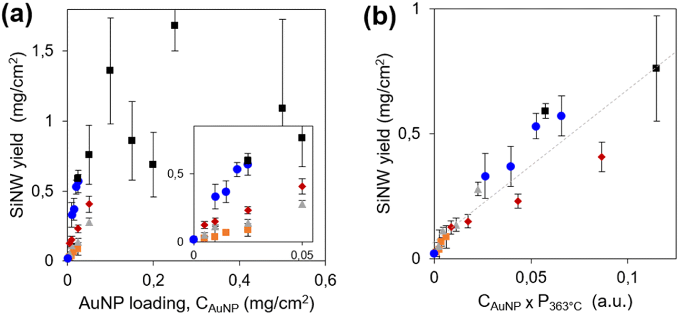 | ||
| Fig. 1 Silicon nanowire yield, expressed as the areal concentration in silicon, as a function of the gold seed loading, CAuNP, (a) and as a function of CAuNP × P363°C where P363°C is the pressure at 363 °C in the reactor (b). Seeds were 1–3 nm AuNPs. Diphenylsilane loading in the reactor: 1 mL (yellow squares), 4 mL (gray triangles, red diamonds), 6 mL (blue circles, black squares). The dotted line is the best linear correlation for all samples with CAuNP < 0.12 mg cm−2 (R2 = 0.91). | ||
Thanks to the very high quality and reproducibility of the growth process in these conditions, we could infer interesting mechanistic details on the growth mechanism. The mass of SiNWs is proportional to their number, determined by the number of seeds CAuNP, and to their average length, determined by the growth rate. Following eqn (4), the growth rate is proportional to the partial pressure of silane,18pSiH4. We estimate pSiH4 from the global pressure P just before growth starts. Indeed, when the temperature attains 363 °C, after 10 minutes heating, the AuNP catalysts are not yet active. Diphenylsilane would turn to silane via the disproportionation reactions (1)–(3), for which we assume a chemical dynamics of global order α in the form pSiH4 ∝ pDPSα, where pDPS is the partial pressure in diphenylsilane. Disproportionation is slow at low temperature42 so that the gas phase consists mainly in diphenylsilane, and the total pressure P363°C is close to pDPS. Thus, pSiH4 at the start of growth would scale as: pSiH4 ∝ (P363°C)α, where α is expected in the range 3–4, depending on the relative rates of reactions (1)–(3). We plot the SiNW areal density vs. CAuNP × (P363°C)α for all growth conditions with various values of α. The 5 series gather onto a common line only for α = 1 (Fig. 1b), showing that the reaction is of apparent first order. A first order dynamics is a very surprising result in view of the disproportionation mechanism, which involves second order steps (1)–(3).
Alternatively, organosilanes can undergo homolytic decomposition,44–47 a first order reaction yielding highly reactive silylenes. Thermal homolysis into silylene was mainly reported at higher temperature (above 600 °C), but the high substitution of Ph2Si could considerably stabilize the di-radical, as for the trityl radical, and thus lower the energy barrier. Additionally, the high pressure in our reactor will increase the rate of homolysis, as previously reported.48 Homolytic decomposition of phenylsilane was reported44,48 to follow two simultaneous paths:
| PhSiH3 → PhSiH + H2 | (5) |
| PhSiH3 → H2Si + C6H6, | (6) |
| Ph2SiH2 → Ph2Si + H2 | (7) |
| Ph2SiH2 → PhSiH + C6H6. | (8) |
Indeed, analysis of the by-products of SiNW growth by GC-MS (Fig. S3†) showed the formation of hydrogen, as expected, and of benzene, the presence of which is not explained by the disproportionation mechanism. Benzene is detected at a low but constant yield, showing that reaction (8) represents about 5% of diphenylsilane decomposition. If the relative frequencies of paths (7) and (8) follow the tendency measured for phenylsilane homolytic paths (5) and (6), it would mean that about 40% of diphenylsilane decomposes by thermal homolysis. Thus, based on our chemical dynamics data and by-product analysis, we propose for SiNW growth from diphenylsilane a mechanism involving homolytic cleavage following reactions (7) and (8) even at the surprisingly low temperature of 430 °C, in addition to the usually cited23,43,49 disproportionation reaction.
As a second parameter, we optimized the SiNW diameter to shift their light absorption in the visible range. The SiNW diameter is known to depend on the AuNP catalyst size in CVD processes.34,40 Using three synthesis methods, we synthesized AuNP colloids within a wide range of sizes, with a narrow size distribution (Fig. 2b). Small AuNPs (3 nm) were synthesized with dodecanethiol stabilization in an organic solvent while bigger AuNPs (12–80 nm) were made in water with citrate stabilization. AuNP solutions were drop cast on the PCS and submitted to SiNW growth. SiNWs of increasing diameters (Fig. 2c and d) grew from all seeds. The PCS-SiNW are homogeneously covered with straight SiNWs, while the samples remain porous (Fig. 2e and f). The SiNW diameter does not increase linearly with the AuNP size. Indeed, the silane pressure in the reactor is a second stringent condition determining the SiNW diameter.18,34 Here the reactor loading, and thus the silane pressure profile during the growth, was set to a medium value, limiting the growth of SiNWs larger than 50 nm, but allowing higher growth rates.
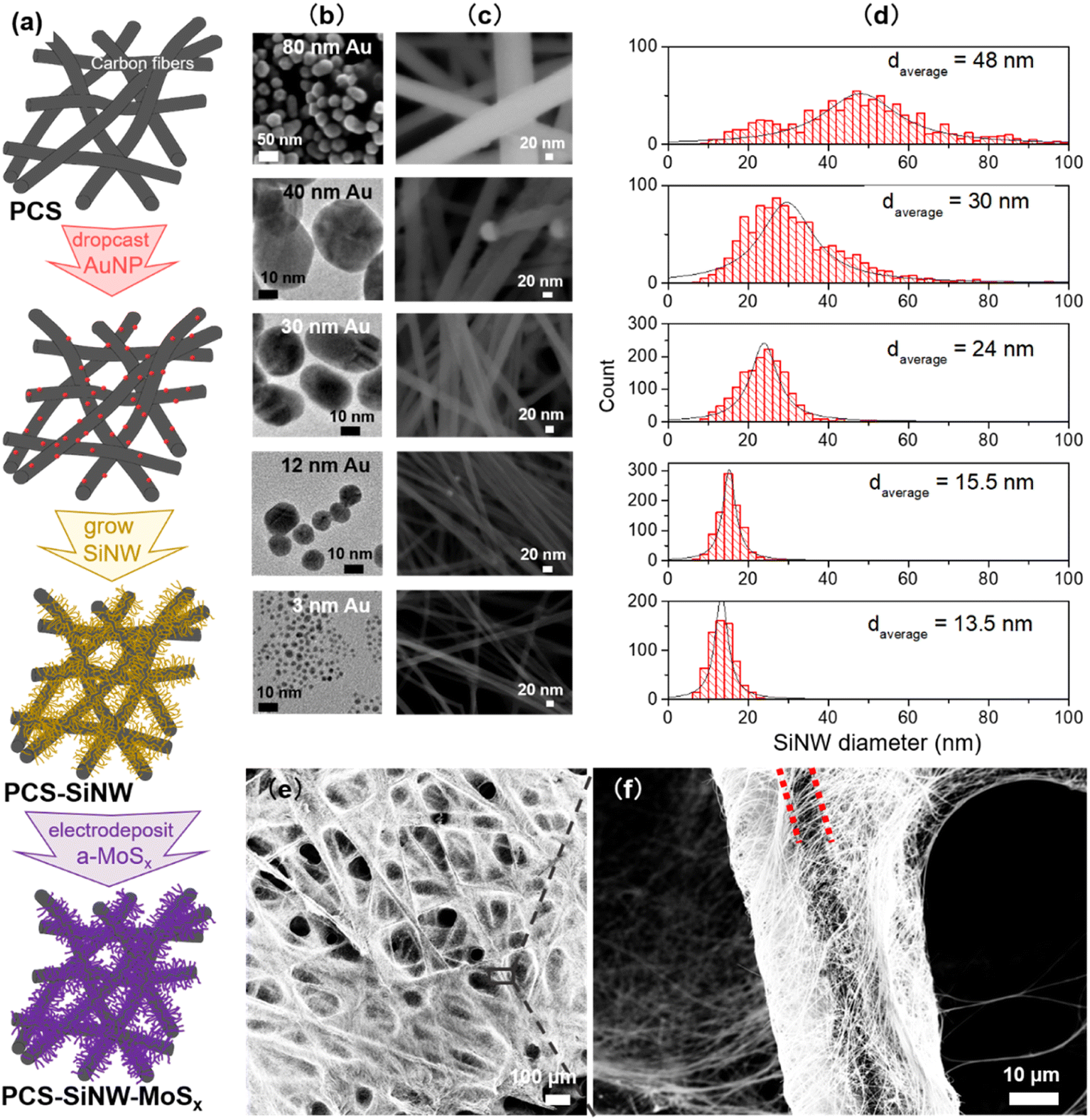 | ||
| Fig. 2 Tuning SiNW diameter by the size of AuNPs: (a) scheme of the PCS-SiNW-MoSx photocathode fabrication. SEM and TEM images of the AuNPs of size 3–80 nm (b) and the subsequent SiNWs grown from them (c); (d) corresponding SiNW diameter histograms (>500 counts); SEM images of the PCS-SiNW (e) and close up view of a single carbon fiber (f). Red dotted lines highlight the diameter of the carbon fiber. | ||
The diameter of the SiNWs determines their absorption wavelength.50 Accordingly, from SiNWs of diameter 13 to 42 nm, PCS-SiNW shifted from a dark bluish to yellowish colour (Fig. 3a), and the absorption spectra of SiNWs, scratched from PCS-SiNW and suspended in dichloromethane, show a progressive blue shift of the plasmon resonance51 band as the SiNW diameter increases (Fig. 3b). Spectrophotometry could however not distinguish light absorption, useful for photoelectrocatalysis, from light diffusion or reflection by the SiNWs. The light absorption of SiNWs was thus simulated numerically using the Finite Element Method (FEM, Comsol Multiphysics) (Fig. S1†), as we previously reported.50 The opacity, corresponding to the non-transmitted light as in the absorbance measurement, was calculated for diameters fitting the experimental SiNW sizes (Fig. 3c). The simulated spectra reproduce well the double-shoulder shape of SiNW absorbance, and the shift of the plasmonic peak position with diameter (Fig. 3d). Additionally, the simulated wave (Fig. S1c†) shows that, at the main absorbance peak, the opacity is due to both reflection (20%) and absorption (40%) of the electromagnetic wave by the SiNW. This confirms the relevance of SiNWs as photosensitizers with a tunable absorption range. PCS-SiNW with SiNW diameter 48 nm, harvesting a larger part in the visible range, was selected for photoelectrocatalysis.
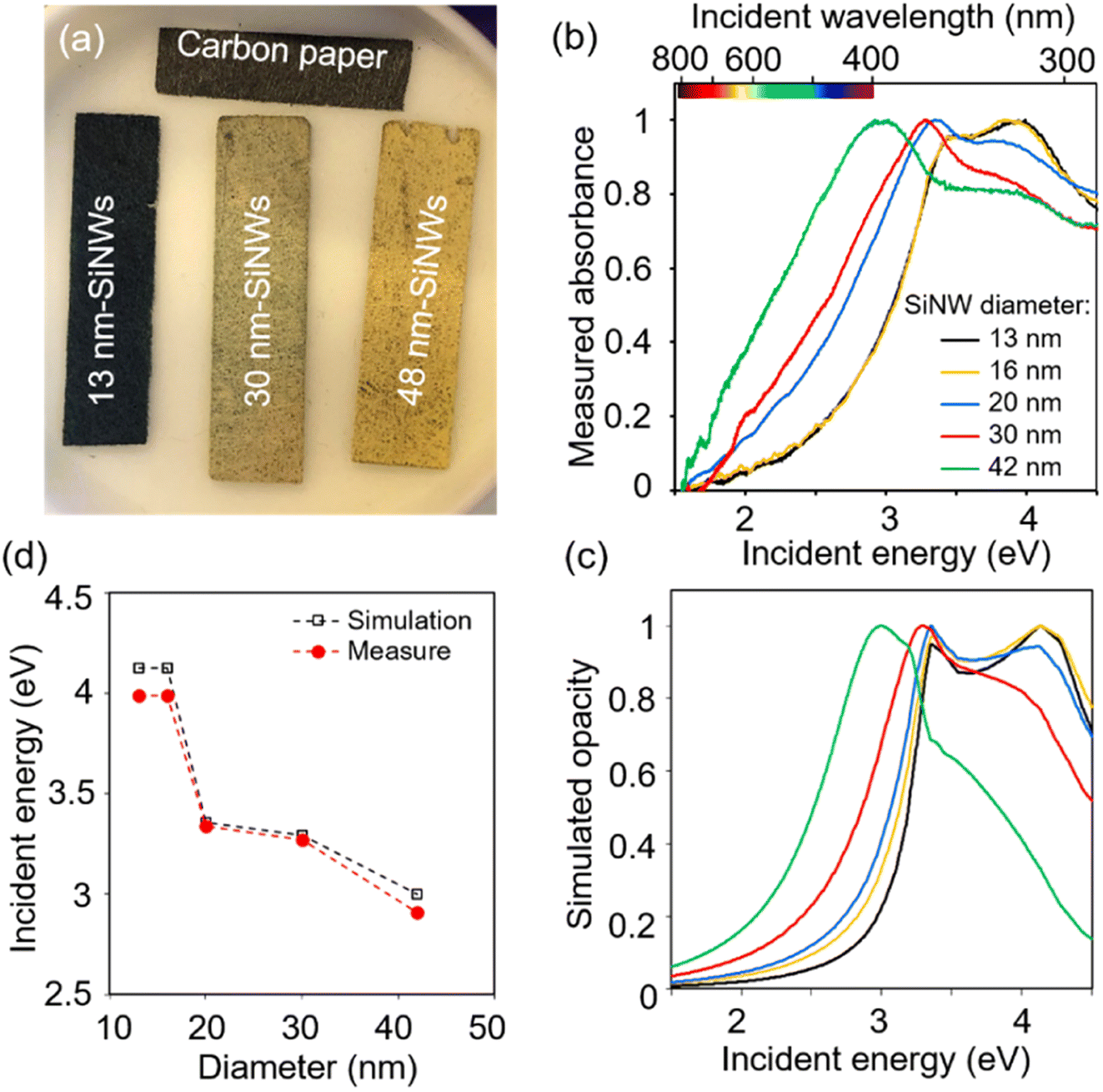 | ||
| Fig. 3 Tuning SiNW absorption wavelength by their diameter: (a) photograph of PCS-SiNW. (b) Normalized spectra of measured absorption for SiNWs from PCS-SiNW with 13, 16, 20, 30 and 42 nm SiNWs. The rainbow indicates the visible range. (c) Normalized spectra of simulated opacity for TE polarization of SiNWs of diameters 13 to 42 nm (same legend as (b)). (d) Position of the plasmonic peak as a function of the SiNW diameter in measured and simulated spectra. | ||
MoSx electrodeposition and sample characterization
a-MoSx was deposited on SiNWs by electrodeposition immediately after nanowire growth. The total charge density that passed through the working electrode (ΔQ) was varied from 0 to 50 mC cm−2 to tune the a-MoSx amount.27 The as-grown 48 nm-SiNWs have a smooth surface (Fig. 4a) which becomes rough after electrodeposition (Fig. 4b). STEM-HAADF imaging shows that a-MoSx forms a shell around the SiNWs (Fig. 4c). Coverage is partly inhomogeneous. EDX (Fig. 4d and e) and EELS (Fig. 4f) confirmed that this layer is composed of Mo and S. The a-MoSx layer can be made thicker by raising the charge passed on SiNWs and reaches several tens of nanometers (Fig. S4†). | ||
| Fig. 4 SEM images of (a) 48 nm-SiNWs, (b) SiNW-MoSx with ΔQ = 6 mC cm−2 (c) HAADF-STEM image of SiNW-MoSx and EDX mapping profile of (d) Si(Kα) and (e) Mo(Kα); (f) STEM-HAADF image and EELS mapping profile of element Si (L edge at 99 eV) and S (L edge at 165 eV); (g, h) High-resolution HAADF-STEM images of a-MoSx. | ||
TEM was used to study the structure of SiNWs and SiNW-MoSx. The as-grown SiNWs present a crystalline silicon core surrounded by an amorphous shell of 1–2 nm (Fig. S5a and b†), which is composed of phenyl moieties23 and a very low degree of oxygen characterized by XPS in our previous work.24 The high-resolution TEM imaging was employed to reveal MoSx atomic structure deposited on this layer. However, conventional TEM would not tell apart the atomic arrangement of MoSx (Fig. S5d†) from the amorphous shell surrounding the SiNWs. With the more sensitive HAADF-STEM technique, images show brighter spots that can be interpreted as Mo atoms on the Si lattice (Fig. 4g and h). Agglomerated a-MoSx particles without well-defined lattice appear in contrast to the silicon core, while fringes present in small regions indicate an amorphous structure with some short-range order (Fig. 4g). The separated nano-sized a-MoSx particles and sub-nano-sized clusters (Fig. 4h) are reminiscent of the a-MoSx structure reported by Tran et al.27 According to their work, a-MoSx particles consist of [Mo3] clusters, in either one-dimensional chains or two-dimensional networks. Here it seems that these particles can scatter over the nanowire surface as in Fig. 4h or agglomerate in a short-range order as in Fig. 4g.
We employed Raman spectroscopy and X-ray diffraction (Fig. 5) to determine the structure of the molybdenum sulfide in PCS-SiNW-MoSx. As the signal from the thin a-MoSx catalytic layer could not be resolved from the signals of PCS and SiNWs, the amount of deposited a-MoSx was increased 100 times for this analysis. Beside the characteristic peak of silicon at 520 cm−1, the Raman spectrum of PCS-SiNW-MoSx (Fig. 5a) shows the full pattern of a-MoSx,27 including S–S vibration bands ν(S–S)t and ν(S–S)br/sh at 510 and 550 cm−1, a bridging ν(Mo3-μS) band at 450 cm−1 and ν(Mo–S) vibration bands at 320, 350 and 370 cm−1.
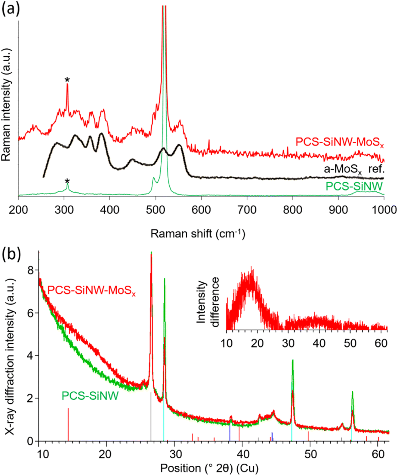 | ||
| Fig. 5 Characterization of electrodeposited a-MoSx: (a) Raman spectra and (b) X-ray diffractograms of PCS-SiNW (green) and PCS-SiNW-MoSx (red). The black line in (a) shows the reference Raman spectrum of a-MoSx (from ref. 27). As collection time was long (10–60 minutes), a known artefact arising from the Raman optics appears on the spectra at 307 cm−1 (labeled as *). Vertical lines in (b) show the reference patterns for graphitic carbon (grey), silicon (cyan), gold (blue) and crystalline MoS2 (red). (b) Inset: X-ray diffraction intensity difference obtained by subtracting the PCS-SiNW from the PCS-SiNW-MoSx diffractogram. | ||
The X-ray diffractogram of PCS-SiNW-MoSx presents the same peaks as the control PCS-SiNW (Fig. 5b), mainly attributed to graphitic carbon from the PCS and crystalline gold and silicon from the SiNWs, except for a wide band at 2θ = 16–19° (Fig. 5b inset). The expected peaks from crystalline MoS2 are not observed. We checked by recording diffractograms both in transmission and reflection that the pattern was the same, showing that the missing MoS2 peaks did not depend on sample orientation. The broad 16–19° band (Fig. 5b inset) indicates a purely amorphous structure with a nearest neighbor distance of 0.26 nm, slightly higher than that of crystalline MoS2 (ref. 52) (0.25 nm) and consistent with Mo–S bond lengths reported for reference a-MoSx catalyst.53
PEC performance of SiNW-MoSx
Photoelectrocatalytic (PEC) performance were measured in 0.5 M H2SO4 under chopped illumination of simulated AM 1.5G sunlight (100 mW cm−2) using a three-electrode configuration. Illuminating PCS-SiNW resulted in a slight positive shift of the open circuit potential, indicating a p-type conductivity that is usually observed in undoped SiNWs.54,55 The current–voltage (J–V) curve of PCS-SiNW-MoSx under chopped illumination was compared with that of PCS-SiNW and PCS-MoSx as controls (Fig. 6a). On one hand, PCS-MoSx shows a high electrocatalytic activity but no photocurrent. On the other hand, PCS-SiNW produces a very low photocurrent (0.02 mA cm−2 at −0.4 V vs. RHE) with an onset at −0.15 V vs. RHE. The PCS-SiNW-MoSx photocathode (ΔQ = 6 mC cm−2 for a-MoSx electrodeposition) exhibits a much higher photocurrent of 0.23 mA cm−2 at −0.15 V vs. RHE and an anodic shift of the onset potential by 0.1 V, demonstrating that a-MoSx catalyst accelerates the electron transport significantly from undoped SiNWs to the electrolyte to convert protons into H2. In general, we observed that the dark current for H2 evolution for PCS-SiNW-MoSx cathode is cathodically shifted with regards to the PCS-MoSx control, highlighting the intrinsic resistance of the undoped SiNWs.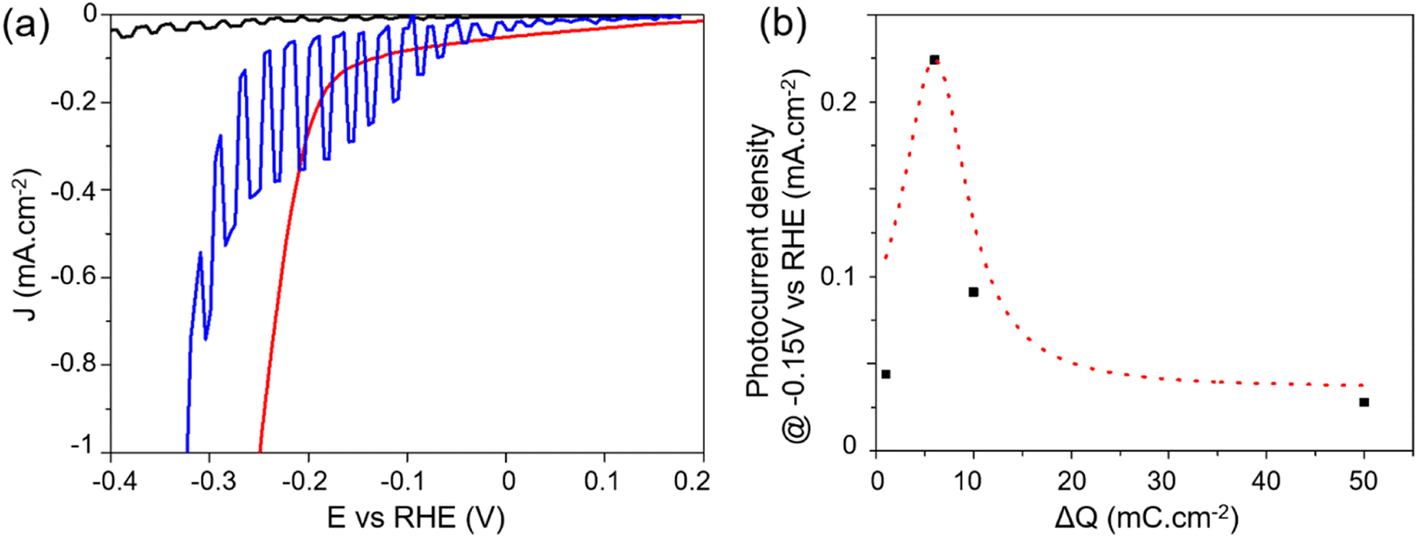 | ||
| Fig. 6 Photoelectrocatalysis performance of PCS-SiNW-MoSx with 48 nm-SiNWs: (a) J–V curves of PCS-SiNW-MoSx (blue), PCS-SiNW (black) and PCS-MoSx (red) electrodes in 0.5 M H2SO4 electrolyte under chopped illumination (a-MoSx deposition: ΔQ = 6 mC cm−2). (b) Photocurrent density of PCS-SiNW-MoSx at −0.15 V vs. RHE as a function of ΔQ during a-MoSx electrodeposition (J–V curves in Fig. S5†). The Gaussian dotted line is a guide to the eye. | ||
A thin passivation layer surrounding the SiNWs proved necessary in producing a PEC photocurrent from silicon-based photocathodes.56,57 Here, the passivation is provided by the native organic shell of phenyls, brought by the diphenylsilane reagents during growth, able to slow down Si oxidation.24,58 We observed a 17% degraded PEC performance (Fig. S6a†) when delaying the a-MoSx deposition 2 weeks after SiNW growth, which lets a limited oxidation happen on the SiNW surface. More, etching the SiNW surface by dissolution in an HF solution before a-MoSx deposition resulted in a complete loss of PEC performance. As a further check, we prepared PCS-SiNW-MoSx electrodes devoid of hydrophobic shell using a conventional SiNW CVD growth method59 fed with SiH4. In this process, the native Si:H surface on SiNWs rapidly turns to oxide once in contact with air. The CVD growth parameters were first optimized to fit the SiNW diameter and areal density with the best PCS-SiNW-MoSx electrodes produced in this study. Then MoSx was deposited on the obtained PCS-SiNW, but no photocurrent was recorded from these samples (Fig. S6b†). Let us note that a much larger current was recorded during the a-MoSx electrodeposition step, probably due to silicon oxidation. These data indicate that an as low as possible SiO2 layer and the presence of a protective shell on the SiNWs play a vital role in the stability of the silicon–catalyst interface.
As expected, comparing PCS-SiNW-MoSx photocathodes with 13 nm- and 48 nm-SiNWs (Fig. S7†) proved that the largest SiNWs provide a 5-fold higher photocurrent than the smaller (0.25 vs. 0.05 mA cm−2 at −0.15 V vs. RHE) while the photocurrent onset is similar (−0.05 V vs. RHE). The optimal areal density of silicon was found similar for all SiNW diameter tested (Fig. S8†). The PEC activity of PCS-SiNW-MoSx photocathode depends much more strongly on the amount of a-MoSx deposited on SiNWs, following a volcano-shaped curve (Fig. 6b). The a-MoSx loading at the optimum ΔQ = 6 mC cm−2 is 31 nmol cm−2 assuming a 2e− oxidation process from [MoS4]2− precursor to a-MoSx. As seen by electron microscopy, this optimal layer consists of an inhomogeneous layer shelling partially the SiNWs. A full coverage of the SiNWs by a-MoSx is obtained at higher loading (Fig. S4d†), but the PEC performance drops, maybe due to a lack of conductivity within thick a-MoSx layers.
The stability of the PCS-SiNW-MoSx photocathode was examined by chronoamperometry analysis at −0.15 V vs. RHE (Fig. 7a and S9b†). The photocurrent dropped by 25–50% after 1 hour, depending on the sample. Gas chromatography analysis of the cell headspace allowed to determine a faradaic yield 98 ± 5% for hydrogen production after 1 hour (Fig. S9†). SEM images of the sample before and after chronoamperometry (Fig. 7b and c) show a change in morphology of the MoSx film: initially wrapping individual SiNWs, the film bundles up substantially the nearby SiNWs after PEC. Detachment and re-aggregation of small a-MoSx nanoparticles was often observed in a-MoSx film as HER catalyst in acid.60,61 This film could clog the electrode porosity and prevent electrolyte access to the internal part. Long-term oxidation of SiNWs by water during PEC could be another reason for the drop in photocurrent.
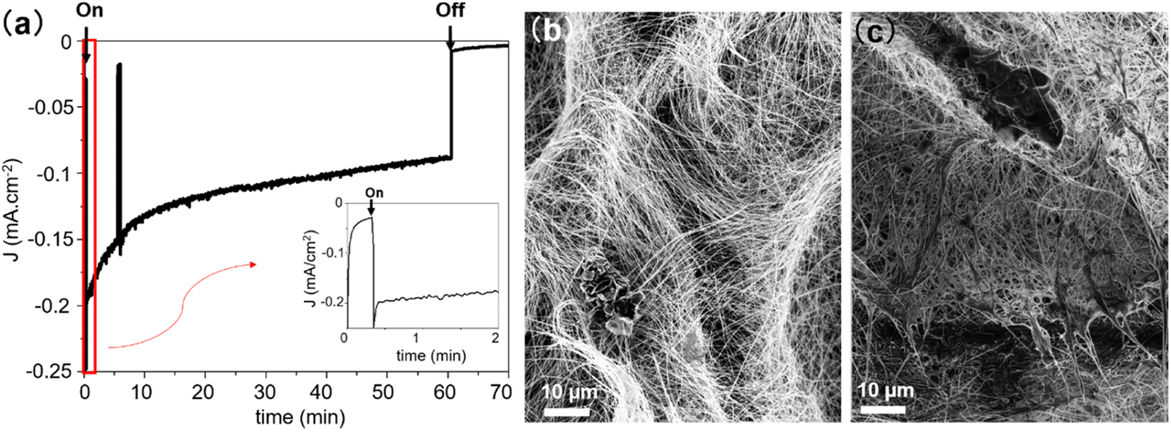 | ||
| Fig. 7 (a) Chronoamperometry of PCS-SiNW-MoSx at −0.15 V vs. RHE in 0.5 M H2SO4 under illumination (48 nm-SiNWs, ΔQMoSx = 6 mC cm−2) with N2 bubbling. SEM images of the electrode before (b) and after (c) the stability test. | ||
Conclusion
In summary, a facile route has been proposed to develop operational porous photocathodes based on SiNWs as light absorbers and MoSx as the HER catalyst. SiNWs were grown in direct contact with the carbon porous conductive support via a low-cost and tunable chemical method, applicable to other porous substrates with various morphology. Our well-controlled growth process allowed optimizing the efficiency of SiNW light absorption by fine-tuning their diameter and thus their absorption spectrum. It also provides a native hydrophobic passivation layer on silicon preventing oxidation, which appears essential in photoelectrocatalysis, probably by ensuring a low-barrier electrical contact between light absorber and catalyst. As compared to other non-noble metal photocatalytic systems on undoped silicon,62 the PCS-SiNW-MoSx photocathode exhibits an interesting photocurrent of 0.23 mA cm−2 at −0.15 V vs. RHE. Further work will focus on doping the SiNWs13 and the a-MoSx catalyst63 to maximize the anodic shift of the onset potential, and design new growth seeds to investigate SiNWs with diameters in the 50–100 nm range. As the hydrophobic protective layer natively grown on the SiNWs proved to prevent oxidation in air and water, we will improve the durability of this shell by enhancing its passivating efficiency, as reported for bulk silicon photocathodes.58 Finally, this work provides a new scalable approach to develop porous photocathode based on easily tunable silicon nanostructures and noble-metal-free HER catalyst.Author contributions
J. W. prepared the samples and wrote the first manuscript. J. W., P. E. O. and C. K. grew the AuNPs of varied sizes. J. W. and H. O. performed the electron microscopy. J. W., P. E. O. and A. M. performed the photoelectrochemical tests. D. N. N. designed the photoelectrochemical tests. M. D. and P. G. designed and realized the CVD growth of the SiNW samples without phenyl protective layer. S. P. designed and performed the XRD characterization. P. C. measured the absorption spectra and wrote the manuscript. V. R. designed and performed the Raman characterization. M. B. and Y. P. designed and realized the finite element simulation of light absorption. H. J., A. M., V. A. and P. C. conceived and designed the experiments, and ensured supervision and funding. All authors discussed the results and commented on the manuscript.Conflicts of interest
There are no conflicts to declare.Acknowledgements
J. W. and P. E. O. acknowledge the financial support from European Horizon 2020's Project Sun-to-X under agreement no. 883264. This work was supported by the Agence Nationale de la Recherche (Labex ARCANE, CBH-EUR-GS, ANR-17-EURE-0003). M. B. and Y. P. acknowledges the financial support from the project PRCE-ANR-POCOMA under agreement ref. ANR-21-CE09-0040-01. The authors thank Adeline Jorge-Robin and Jennifer Fize for GC-MS and GC quantitative analyses.References
- G. Segev, C. Hahn, Z. J. Xu, W.-H. Cheng, T. G. Deutsch, C. Xiang, J. Z. Zhang, L. Hammarström, D. G. Nocera, A. Z. Weber, P. Agbo, T. Hisatomi, F. E. Osterloh, K. Domen, F. F. Abdi, S. Haussener, D. J. Miller, S. Ardo, P. C. McIntyre, T. Hannappel, S. Hu, H. Atwater, J. M. Gregoire, M. Z. Ertem, I. D. Sharp, K.-S. Choi, J. S. Lee, O. Ishitani, J. W. Ager, R. R. Prabhakar, A. T. Bell, S. W. Boettcher, K. Vincent, K. Takanabe, V. Artero, R. Napier, B. R. Cuenya, M. T. M. Koper, R. V. D. Krol and F. Houle, The 2022 Solar Fuels Roadmap, J. Phys. D: Appl. Phys., 2022, 55(32), 323003, DOI:10.1088/1361-6463/ac6f97.
- M. G. Walter, E. L. Warren, J. R. McKone, S. W. Boettcher, Q. Mi, E. A. Santori and N. S. Lewis, Solar Water Splitting Cells, Chem. Rev., 2010, 110(11), 6446–6473, DOI:10.1021/cr1002326.
- M. Caretti, E. Mensi, R.-A. Kessler, L. Lazouni, B. Goldman, L. Carbone, S. Nussbaum, R. A. Wells, H. Johnson, E. Rideau, J. Yum and K. Sivula, Transparent Porous Conductive Substrates for Gas-Phase Photoelectrochemical Hydrogen Production, Adv. Mater., 2208740, DOI:10.1002/adma.202208740.
- G. Zafeiropoulos, H. Johnson, S. Kinge, M. C. M. van de Sanden and M. N. Tsampas, Solar Hydrogen Generation from Ambient Humidity Using Functionalized Porous Photoanodes, ACS Appl. Mater. Interfaces, 2019, 11(44), 41267–41280, DOI:10.1021/acsami.9b12236.
- J. Rongé, S. Deng, S. Pulinthanathu Sree, T. Bosserez, S. W. Verbruggen, N. Kumar Singh, J. Dendooven, M. B. J. Roeffaers, F. Taulelle, M. De Volder, C. Detavernier and J. A. Martens, Air-Based Photoelectrochemical Cell Capturing Water Molecules from Ambient Air for Hydrogen Production, RSC Adv., 2014, 4(55), 29286–29290, 10.1039/C4RA05371K.
- L. Wei, R. Li, Q. Fan, C. Yu and P. Tan, Fabrication of P-Type Silicon Nanowire Array Based Photoelectrodes for the Efficient Photoelectrocatalytic Reduction of CO2 to Fuels and Chemicals, Sustain. Energy Fuels, 2022, 6(8), 1854–1865, 10.1039/D2SE00105E.
- S. W. Boettcher, J. M. Spurgeon, M. C. Putnam, E. L. Warren, D. B. Turner-Evans, M. D. Kelzenberg, J. R. Maiolo, H. A. Atwater and N. S. Lewis, Energy-Conversion Properties of Vapor-Liquid-Solid–Grown Silicon Wire-Array Photocathodes, Science, 2010, 327(5962), 185–187 CrossRef CAS PubMed.
- A. P. Goodey, S. M. Eichfeld, K.-K. Lew, J. M. Redwing and T. E. Mallouk, Silicon Nanowire Array Photoelectrochemical Cells, J. Am. Chem. Soc., 2007, 129(41), 12344–12345 CrossRef CAS PubMed.
- I. Oh, J. Kye and S. Hwang, Enhanced Photoelectrochemical Hydrogen Production from Silicon Nanowire Array Photocathode, Nano Lett., 2012, 12(1), 298–302 CrossRef CAS.
- S. Chandrasekaran, S. J. P. McInnes, T. J. MacDonald, T. Nann and N. H. Voelcker, Porous Silicon Nanoparticles as a Nanophotocathode for Photoelectrochemical Water Splitting, RSC Adv., 2015, 5(104), 85978–85982, 10.1039/c5ra12559f.
- T. Xu, Y. Lambert, C. Krzeminski, B. Grandidier, D. Stiévenard, G. Lévêque, A. Akjouj, Y. Pennec and B. Djafari-Rouhani, Optical Absorption of Silicon Nanowires, J. Appl. Phys., 2012, 112(3) DOI:10.1063/1.4739708.
- K.-Q. Peng, X. Wang, L. Li, Y. Hu and S.-T. Lee, Silicon Nanowires for Advanced Energy Conversion and Storage, Nano Today, 2013, 8(1), 75–97, DOI:10.1016/j.nantod.2012.12.009.
- P. D. Tran, S. S. Pramana, V. S. Kale, M. Nguyen, S. Y. Chiam, S. K. Batabyal, L. H. Wong, J. Barber and J. Loo, Novel Assembly of an MoS 2 Electrocatalyst onto a Silicon Nanowire Array Electrode to Construct a Photocathode Composed of Elements Abundant on the Earth for Hydrogen Generation, Chem.–Eur. J., 2012, 18(44), 13994–13999, DOI:10.1002/chem.201202214.
- S. Chandrasekaran, T. Nann and N. H. Voelcker, Silicon Nanowire Photocathodes for Photoelectrochemical Hydrogen Production, Nanomaterials, 2016, 6(8), 1–7, DOI:10.3390/nano6080144.
- B. M. Bang, H. Kim, H.-K. Song, J. Cho and S. Park, Scalable Approach to Multi-Dimensional Bulk Si Anodes via Metal-Assisted Chemical Etching, Energy Environ. Sci., 2011, 4(12), 5013–5019, 10.1039/C1EE02310A.
- F. J. Wendisch, M. Rey, N. Vogel and G. R. Bourret, Large-Scale Synthesis of Highly Uniform Silicon Nanowire Arrays Using Metal-Assisted Chemical Etching, Chem. Mater., 2020, 32(21), 9425–9434, DOI:10.1021/acs.chemmater.0c03593.
- S. Imtiaz, I. S. Amiinu, D. Storan, N. Kapuria, H. Geaney, T. Kennedy and K. M. Ryan, Dense Silicon Nanowire Networks Grown on a Stainless-Steel Fiber Cloth: A Flexible and Robust Anode for Lithium-Ion Batteries, Adv. Mater., 2021, 2105917, DOI:10.1002/adma.202105917.
- V. Schmidt, J. V. Wittemann and U. Gösele, Growth, Thermodynamics, and Electrical Properties of Silicon Nanowires, Chem. Rev., 2010, 110(1), 361–388, DOI:10.1021/cr900141g.
- H.-Y. Tuan and B. A. Korgel, Importance of Solvent-Mediated Phenylsilane Decompositon Kinetics for High-Yield Solution-Phase Silicon Nanowire Synthesis, Chem. Mater., 2008, 20(4), 1239–1241, DOI:10.1021/cm7033068.
- A. T. Heitsch, D. D. Fanfair, H.-Y. Tuan and B. A. Korgel, Solution−Liquid−Solid (SLS) Growth of Silicon Nanowires, J. Am. Chem. Soc., 2008, 130(16), 5436–5437, DOI:10.1021/ja8011353.
- J. C. Chan, H. Tran, J. W. Pattison and S. B. Rananavare, Facile Pyrolytic Synthesis of Silicon Nanowires, Solid-State Electron., 2010, 54(10), 1185–1191, DOI:10.1016/j.sse.2010.05.011.
- J. D. Holmes, K. P. Johnston, R. C. Doty and B. A. Korgel, Control of Thickness and Orientation of Solution-Grown Silicon Nanowires, Science, 2000, 287, 1471–1473 CrossRef CAS PubMed.
- O. Burchak, C. Keller, G. Lapertot, M. Salaün, J. Danet, Y. Chen, N. Bendiab, B. Pépin-Donat, C. Lombard, J. Faure-Vincent, A. Vignon, D. Aradilla, P. Reiss and P. Chenevier, Scalable Chemical Synthesis of Doped Silicon Nanowires for Energy Applications, Nanoscale, 2019, 11(46), 22504–22514, 10.1039/c9nr03749g.
- S. Karuppiah, C. Keller, P. Kumar, P. H. Jouneau, D. Aldakov, J. B. Ducros, G. Lapertot, P. Chenevier and C. Haon, A Scalable Silicon Nanowires-Grown-On-Graphite Composite for High-Energy Lithium Batteries, ACS Nano, 2020, 14(9), 12006–12015, DOI:10.1021/acsnano.0c05198.
- P. C. K. Vesborg, B. Seger and I. Chorkendorff, Recent Development in Hydrogen Evolution Reaction Catalysts and Their Practical Implementation, J. Phys. Chem. Lett., 2015, 6(6), 951–957, DOI:10.1021/acs.jpclett.5b00306.
- D. Merki, S. Fierro, H. Vrubel and X. Hu, Amorphous Molybdenum Sulfide Films as Catalysts for Electrochemical Hydrogen Production in Water, Chem. Sci., 2011, 2(7), 1262–1267, 10.1039/C1SC00117E.
- P. D. Tran, T. V. Tran, M. Orio, S. Torelli, Q. D. Truong, K. Nayuki, Y. Sasaki, S. Y. Chiam, R. Yi, I. Honma, J. Barber and V. Artero, Coordination Polymer Structure and Revisited Hydrogen Evolution Catalytic Mechanism for Amorphous Molybdenum Sulfide, Nat. Mater., 2016, 15(6), 640–646, DOI:10.1038/nmat4588.
- G.-L. Zang, G.-P. Sheng, C. Shi, Y.-K. Wang, W.-W. Li and H.-Q. Yu, A Bio-Photoelectrochemical Cell with a MoS3-Modified Silicon Nanowire Photocathode for Hydrogen and Electricity Production, Energy Environ. Sci., 2014, 7(9), 3033–3039, 10.1039/C4EE00654B.
- D. Hu, J. Xiang, Q. Zhou, S. Su, Z. Zhang, X. Wang, M. Jin, L. Nian, R. Nözel, G. Zhou, Z. Zhang and J. Liu, One-Step Chemical Vapor Deposition of MoS2 Nanosheets on SiNWs as Photocathodes for Efficient and Stable Solar-Driven Hydrogen Production, Nanoscale, 2018, 10(7), 3518–3525, 10.1039/C7NR09235K.
- G. Paulraj, P. S. Venkatesh, P. Dharmaraj, S. Gopalakrishnan and K. Jeganathan, Stable and Highly Efficient MoS2/Si NWs Hybrid Heterostructure for Photoelectrocatalytic Hydrogen Evolution Reaction, Int. J. Hydrogen Energy, 2020, 45(3), 1793–1801, DOI:10.1016/j.ijhydene.2019.11.051.
- C.-J. Chen, K.-C. Yang, C.-W. Liu, Y.-R. Lu, C.-L. Dong, D.-H. Wei, S.-F. Hu and R.-S. Liu, Silicon Microwire Arrays Decorated with Amorphous Heterometal-Doped Molybdenum Sulfide for Water Photoelectrolysis, Nano Energy, 2017, 32, 422–432, DOI:10.1016/j.nanoen.2016.12.045.
- L. Zhang, C. Liu, A. B. Wong, J. Resasco and P. Yang, MoS2-Wrapped Silicon Nanowires for Photoelectrochemical Water Reduction, Nano Res., 2015, 8(1), 281–287, DOI:10.1007/s12274-014-0673-y.
- Z. Huang, C. Wang, L. Pan, F. Tian, X. Zhang and C. Zhang, Enhanced Photoelectrochemical Hydrogen Production Using Silicon Nanowires@MoS3, Nano Energy, 2013, 2(6), 1337–1346, DOI:10.1016/j.nanoen.2013.06.016.
- C. Keller, A. Desrues, S. Karuppiah, E. Martin, J. P. Alper, F. Boismain, C. Villevieille, N. Herlin-Boime, C. Haon and P. Chenevier, Effect of Size and Shape on Electrochemical Performance of Nano-Silicon-Based Lithium Battery, Nanomaterials, 2021, 11(2), 1–15, DOI:10.3390/nano11020307.
- M. Brust, M. Walker, D. Bethell, D. J. Schiffrin and R. Whyman, Synthesis of Thiol-Derivatised Gold Nanoparticles in a Two-Phase Liquid–Liquid System, J. Chem. Soc. Chem. Commun., 1994, 7, 801–802 RSC.
- J. Turkevich, P. C. Stevenson and J. Hillier, A Study of the Nucleation and Growth Processes in the Synthesis of Colloidal Gold, J. Phys. Chem. Lett., 1951, 11, 55–75, 10.1039/DF9511100055.
- C. Ziegler and A. Eychmuller, Seeded Growth Synthesis of Uniform Gold Nanoparticles with Diameters of 15− 300 Nm, J. Phys. Chem. C, 2011, 115(11), 4502–4506 CrossRef CAS.
- D. N. Nguyen, M. Fadel, P. Chenevier, V. Artero and P. D. Tran, Water-Splitting Artificial Leaf Based on a Triple-Junction Silicon Solar Cell: One-Step Fabrication through Photoinduced Deposition of Catalysts and Electrochemical Operando Monitoring, J. Am. Chem. Soc., 2022, 144(22), 9651–9660, DOI:10.1021/jacs.2c00666.
- P. Reiss, M. Carrière, C. Lincheneau, L. Vaure and S. Tamang, Synthesis of Semiconductor Nanocrystals, Focusing on Nontoxic and Earth-Abundant Materials, Chem. Rev., 2016, 116(18), 10731–10819, DOI:10.1021/acs.chemrev.6b00116.
- U. Langklotz, T. Lein, C. Schulze, M. Weiser, A. Krause and A. Michaelis, Scalable Fabrication of Gold Nanoparticles with Adjustable Size Distribution as Catalytic Nuclei for the CVD Growth of Silicon Nanowires, Appl. Surf. Sci., 2020, 502, 144203 CrossRef CAS.
- F. Dhalluin, P. J. Desré, M. I. den Hertog, J.-L. Rouvière, P. Ferret, P. Gentile and T. Baron, Critical Condition for Growth of Silicon Nanowires, J. Appl. Phys., 2007, 102(9), 94906, DOI:10.1063/1.2811935.
- H. Gilman and D. H. Miles, Disproportionation Reaction of Diphenylsilane in the Absence of Any Added Catalyst, J. Org. Chem., 1958, 23, 326–328, DOI:10.1021/jo01096a626.
- D. C. Lee, T. Hanrath and B. A. Korgel, The Role of Precursor-Decomposition Kinetics in Silicon-Nanowire Synthesis in Organic Solvents, Angew Chem. Int. Ed. Engl., 2005, 44(23), 3573–3577, DOI:10.1002/anie.200463001.
- H. E. O'Neal, M. A. Ring, D. Kim and K. D. King, Primary Reaction Channels and Kinetics of the Thermal Decomposition of Phenylsilane, J. Phys. Chem., 1995, 99, 9397–9402 CrossRef.
- M. A. Ring and H. E. O'Neal, Mechanism of the Thermally Induced Gas-Phase Decomposition of Silane: A Revisitation, J. Phys. Chem., 1992, 96(26), 10848–10855 CrossRef CAS.
- R. E. Jardine, H. E. O'Neal, M. A. Ring and M. E. Beatie, Mechanism of the Thermal Decomposition of Ethylsilane, J. Phys. Chem., 1995, 99(33), 12507–12511 CrossRef CAS.
- K. L. Walker, R. E. Jardine, M. A. Ring and H. E. O'Neal, Mechanisms and Kinetics of the Thermal Decompositions of Trichlorosilane, Dichlorosilane, and Monochlorosilane, Int. J. Chem. Kinet., 1998, 30(1), 69–88 CrossRef CAS.
- J. J. Nájera, J. O. Cáceres and S. I. Lane, Gas-Phase Infrared Laser Photolysis of Phenylsilane, J. Photochem. Photobiol., A, 2000, 131(1), 1–11, DOI:10.1016/S1010-6030(99)00215-4.
- G. Flynn, K. Stokes and K. M. Ryan, Low Temperature Solution Synthesis of Silicon, Germanium and Si–Ge Axial Heterostructures in Nanorod and Nanowire Form, Chem. Commun., 2018, 54(45), 5728–5731, 10.1039/C8CC03075H.
- T. Xu, Y. Lambert, C. Krzeminski, B. Grandidier, D. Stiévenard, G. Lévêque, A. Akjouj, Y. Pennec and B. Djafari-Rouhani, Optical Absorption of Silicon Nanowires, J. Appl. Phys., 2012, 112(3), 033506, DOI:10.1063/1.4739708.
- P. Reiss, M. Carrière, C. Lincheneau, L. Vaure and S. Tamang, Synthesis of Semiconductor Nanocrystals, Focusing on Nontoxic and Earth-Abundant Materials, Chem. Rev., 2016, 116(18), 10731–10819, DOI:10.1021/acs.chemrev.6b00116.
- J. L. Grosseau-Poussard, P. Moine and J. P. Villain, Microstructural and Tribological Characterization of MoSx Coatings Produced by High-Energy Ion-Beam-Assisted Deposition, Thin Solid Films, 1993, 224(1), 52–57, DOI:10.1016/0040-6090(93)90457-Z.
- P. D. Tran, M. Nguyen, S. S. Pramana, A. Bhattacharjee, S. Y. Chiam, J. Fize, M. J. Field, V. Artero, L. H. Wong, J. Loo and J. Barber, Copper Molybdenum Sulfide: A New Efficient Electrocatalyst for Hydrogen Production from Water, Energy Environ. Sci., 2012, 5(10), 8912, 10.1039/c2ee22611a.
- Y. Wang, K.-K. Lew, T.-T. Ho, L. Pan, S. W. Novak, E. C. Dickey, J. M. Redwing and T. S. Mayer, Use of Phosphine as an N-Type Dopant Source for Vapor−Liquid−Solid Growth of Silicon Nanowires, Nano Lett., 2005, 5(11), 2139–2143, DOI:10.1021/nl051442h.
- M. Legallais, T. T. T. Nguyen, M. Mouis, B. Salem, E. Robin, P. Chenevier and C. Ternon, An Innovative Large Scale Integration of Silicon Nanowire-Based Field Effect Transistors, Solid State Electron., 2018, 143, 97–102, DOI:10.1016/j.sse.2017.11.008.
- S. Chandrasekaran, N. Kaeffer, L. Cagnon, D. Aldakov, J. Fize, G. Nonglaton, F. Baleras, P. Mailley and V. Artero, A Robust ALD-Protected Silicon-Based Hybrid Photoelectrode for Hydrogen Evolution under Aqueous Conditions, Chem. Sci., 2019, 10(16), 4469–4475, 10.1039/C8SC05006F.
- D. G. Boucher, K. Kearney, E. Ertekin and M. J. Rose, Tuning P-Si(111) Photovoltage via Molecule|Semiconductor Electronic Coupling, J. Am. Chem. Soc., 2021, 143(6), 2567–2580, DOI:10.1021/jacs.0c12075.
- B. Wu, T. Wang, B. Liu, H. Li, Y. Wang, S. Wang, L. Zhang, S. Jiang, C. Pei and J. Gong, Stable Solar Water Splitting with Wettable Organic-Layer-Protected Silicon Photocathodes, Nat. Commun., 2022, 13(1), 4460, DOI:10.1038/s41467-022-32099-1.
- P. Gentile, T. David, F. Dhalluin, D. Buttard, N. Pauc, M. D. Hertog, P. Ferret and T. Baron, The Growth of Small Diameter Silicon Nanowires to Nanotrees, Nanotechnology, 2008, 19(12), 125608, DOI:10.1088/0957-4484/19/12/125608.
- A. B. Laursen, P. C. K. Vesborg and I. Chorkendorff, A High-Porosity Carbon Molybdenum Sulphide Composite with Enhanced Electrochemical Hydrogen Evolution and Stability, Chem. Commun., 2013, 49(43), 4965–4967, 10.1039/C3CC41945B.
- L. Zhang, L. Wu, J. Li and J. Lei, Electrodeposition of Amorphous Molybdenum Sulfide Thin Film for Electrochemical Hydrogen Evolution Reaction, BMC Chem., 2019, 13(1), 88, DOI:10.1186/s13065-019-0600-0.
- G. Zeng, T. A. Pham, S. Vanka, G. Liu, C. Song, J. K. Cooper, Z. Mi, T. Ogitsu and F. M. Toma, Development of a Photoelectrochemically Self-Improving Si/GaN Photocathode for Efficient and Durable H2 Production, Nat. Mater., 2021, 20(8), 1130–1135, DOI:10.1038/s41563-021-00965-w.
- A. Morozan, H. Johnson, C. Roiron, G. Genay, D. Aldakov, A. Ghedjatti, C. T. Nguyen, P. D. Tran, S. Kinge and V. Artero, Nonprecious Bimetallic Iron-Molybdenum Sulfide Electrocatalysts for the Hydrogen Evolution Reaction in Proton Exchange Membrane Electrolyzers, ACS Catal., 2020, 14336–14348, DOI:10.1021/acscatal.0c03692.
Footnote |
| † Electronic supplementary information (ESI) available. See DOI: https://doi.org/10.1039/d3se00408b |
| This journal is © The Royal Society of Chemistry 2023 |