
 Open Access Article
 This Open Access Article is licensed under a
 Creative Commons Attribution 3.0 Unported Licence
Influence of Mo doping on interfacial charge carrier dynamics in photoelectrochemical water oxidation on BiVO4†
Xiaofeng
Wu
 a,
Freddy E.
Oropeza
b,
Zheng
Qi
c,
Marcus
Einert
a,
Chuanmu
Tian
a,
Clément
Maheu
a,
Kangle
Lv
c and
Jan P.
Hofmann
*a
a,
Freddy E.
Oropeza
b,
Zheng
Qi
c,
Marcus
Einert
a,
Chuanmu
Tian
a,
Clément
Maheu
a,
Kangle
Lv
c and
Jan P.
Hofmann
*a
aSurface Science Laboratory, Department of Materials and Earth Sciences, Technical University of Darmstadt, Otto-Berndt-Strasse 3, 64287 Darmstadt, Germany. E-mail: hofmann@surface.tu-darmstadt.de
bPhotoactivated Processes Unit, IMDEA Energy Institute, Parque Tecnológico de Móstoles, Avda. Ramón de la Sagra 3, 28935 Móstoles, Madrid, Spain
cLaboratory of Catalysis and Materials Science of the State Ethnic Affairs Commission & Ministry of Education, College of Resources and Environment, South-Central Minzu University, Wuhan 430074, China
First published on 17th May 2023
Abstract
The understanding of interfacial charge transfer processes is vital to the design of efficient photoanodes in photoelectrochemical (PEC) water splitting. Bismuth vanadate (BiVO4) is a promising photoanode material to drive the oxygen evolution reaction (OER). However, intrinsic BiVO4 suffers from a slow charge carrier mobility and sluggish OER kinetics, which gives rise to a high charge carrier recombination rate and unsatisfactory photoelectrochemical performance. Although the impact of metal doping of BiVO4 in the field of photocatalysis and photoelectrochemistry has been investigated in literature, a detailed understanding of the interfacial charge carrier dynamics in dependence of surface configuration is still required for further PEC device optimization. In this work, BiVO4 film samples were prepared by a modified metal organic precursor decomposition method. Effects of molybdenum (Mo) doping on the photocurrent density, electrochemical impedance spectra and interfacial charge transfer kinetics of BiVO4 were investigated. Our results indicate: (1) interfacial charge transfer resistances (Rct) of BiVO4 in 0.1 M phosphate buffer solution decrease 2 to 3 orders of magnitude under illumination. (2) Intensity of the photocurrent is predominantly limited by Rct, rather than the semiconductor bulk resistance (Rbulk). (3) Mo doping does not only increase photovoltage, but also obviously decreases Rct. (4) Compared to pristine BiVO4, Mo doping leads to an enhancement of photocurrent density at 1.23 V vs. RHE to 25.3 μA cm−2, i.e., by a factor 2.7.
1. Introduction
Photoelectrochemical water splitting is regarded as a promising approach to convert and store solar energy in H2.1 Compared to the photocathodic half reaction, the oxygen evolution reaction (OER) in photoelectrochemical water splitting is more complex due to involvement of multiple proton-coupled electron transfer steps.2,3 Monoclinic bismuth vanadate (BiVO4), as a promising photoanode material, has drawn significant attention due to its high absorption coefficient, suitable band edge positions for redox reactions, long charge carrier lifetime and chemical stability.4,5 However, intrinsic BiVO4 still suffers from a low charge carrier mobility, which gives rise to a small diffusion length of holes. According to previous literature, the hole diffusion length of BiVO4 is reported to be 70–100 nm.6–8 Nevertheless, recent study based on a more reliable approach indicated that it may be overestimated and only 15 nm.9 On the other hand, the oxygen evolution reaction (OER) process is kinetically sluggish due to the proton-coupled four-electron transfer at the semiconductor–electrolyte interface.10Morphology control of BiVO4 is an effective approach to overcome the drawback of small carrier diffusion length and therefore has been employed for enhancing photoelectrochemical performance. Up to date, plates, dendrite-like, and worm-like shapes of BiVO4 have been synthesized for increasing the number of active sites and reducing the required migration lengths for charge transfer.11–13 For example, Zou et al. confirmed that the charge carrier separation efficiency of porous worm-like BiVO4 films is twice higher than that of dense BiVO4 films due to lower bulk recombination of the charge carriers.14 On the other hand, lots of works have been dedicated to increase the charge carrier concentration and conductivity of semiconductors by metal/non-metal doping, which can alleviate the disadvantage of small charge carrier mobility.6,15,16
In order to solve the problem of slow reaction kinetics of the OER, loading oxidation co-catalysts, such as IrO2, RuO2, and CoOx, is conventionally considered as a superior strategy, as it can change the reaction paths and lower the activation energy barrier of the rate-determining steps in OER.17,18 For instance, Gong and co-workers achieved a photocurrent of 2.71 mA cm−2 at 1.23 V vs. RHE by loading a moderate amount of Co3O4 on BiVO4, which is 5 times higher than the photocurrent of bare BiVO4.19
Although the influence of doping on the photoelectrochemical performance of BiVO4 has been investigated, a concrete and comprehensive understanding on interfacial charge carrier dynamics is still needed.
In this study, Mo doped BiVO4 photoanodes were prepared by a two-step spin coating-calcination approach. The effect of doping on the photoelectrochemical performance of OER are systemically investigated from the aspect of interfacial resistance and interfacial transfer of charge carriers. We believe that insights into the interfacial charge transfer processes is the key to better understand the roles of dopants on BiVO4 photoanodes in order to further improve the overall PEC performance.
2. Experimental details
2.1 Sample preparation
Pristine BiVO4 films were synthesized by a modified metal organic decomposition method according to literature.20 First, ITO substrates (2 × 2 cm2) were cleaned by sonication in distilled water, acetone, and ethanol for 15 min each and then calcined at 470 °C for 2 h to remove adventitious organic compounds. The ITO substrates were covered with tape at the edge to leave a blank area for later conductive connection. To prepare the precursor solutions, 1 mmol of Bi(NO3)3·5H2O (99.99%, Sigma-Aldrich) was dissolved in 4 mL of 2-methoxyethanol (99.5%, Carl Roth), which forms a colourless solution. 1 mmol of vanadyl-acetylacetonate (98%, Sigma-Aldrich) was dissolved in 4 mL of methanol and forms a dark blue solution. Subsequently, the dark blue solution was carefully added into the bismuth-containing colourless solution. 0.5 mL of acetylacetone (99%, Sigma-Aldrich) was added for adjusting the viscosity of the resulting solution. Finally, 50 μL of this solution was spin coated (1800 rpm, 1 min) on the cleaned ITO substrates. After preheated at 150 °C for 10 min, the substrates were calcined in air at 470 °C for 2 h in a muffle furnace. For Mo doped BiVO4 films, bis(acetylacetonato) dioxomolybdenum(VI) (Sigma-Aldrich) was used as Mo source, a stoichiometric ratio of V to Mo compounds (0.97 mmol: 0.03 mmol) in methanol was prepared as precursor solution. The spin coating and calcination processes are the same to those for pristine BiVO4. The obtained samples were denoted as BVO and Mo-BVO.2.2 Materials characterization
XRD pattern was recorded from 10° to 70° on a Bruker D8 Advance diffractometer with monochromatic Cu Kα radiation (λ = 1.54178 Å) at a scan rate of 0.02° min−1. The morphologies of all samples were assessed by field emission scanning electron microscopy (FESEM, SU8010, Hitachi). UV-Vis-NIR spectra were measured on a Cary 7000 universal measurement spectrometer (Agilent Technologies, Santa Clara, USA). The sample orientation was set as 6° and baseline was corrected against air. The transmission and reflectance spectra were recorded and absorption spectra in percentage were obtained by subtracting transmission and reflectance spectra from 1. X-ray photoelectron spectra (XPS) were recorded on a Thermo Fisher Escalab 250 with a monochromic Al Kα X-ray source (hν = 1486.6 eV) operated at 13 mA and 15 kV. The pressure inside the analytical chamber was monitored below 5 × 10⁻⁹ mbar. The high-resolution core-level spectra were acquired with a pass energy of 10 eV, a step size of 0.05 eV, and a dwell time of 50 ms per measurement point. All XP spectra were calibrated by setting Bi 4f7/2 spectrum to 159.0 eV. An electron gun was used to compensate for surface charging. The reflectance FTIR measurements were performed on a Bruker VERTEX 80v spectrometer, equipped with MCT detector, and the incidence angle was set at 60°. A flat aluminum (Al) mirror was used for background correction. FTIR spectra were acquired at a resolution of 2 cm−1 by averaging 100 scans in the range of 400–4000 cm−1. Raman spectra were obtained from 50 to 3000 cm−1 with excitation wavelength of 514 nm on a micro-Raman HR800 spectrometer (Horiba Jobin Yvon, Bensheim, Germany).Photoelectrochemical characterization was performed in three electrode configuration (PECC-2 cell Zahner Elektrik GmbH, Germany). The working electrodes consisting of BiVO4 film samples were electrically connected by copper tape (Fig. S1†). Ag/AgCl and Pt wire were used as reference electrode and counter electrode, respectively. 0.1 M sodium phosphate buffer solution (KPi, pH 6.8) and 0.5 M sodium sulfite solution were used as electrolytes. The photoelectrochemical performance was evaluated by linear sweep voltammetry which was carried out in a bias range of +0.6 VRHE to +1.8 VRHE at a scan rate of 10 mV. EIS measurements were conducted at +1.2 VRHE by applying a sine 10 mV signal AC amplitude in the frequency range of 0.1 Hz to 10 KHz. Modulated illumination was provided by blue emitting diode (435 nm, 100 mW cm−2) and the irradiation active area was 0.283 cm2. Mott Schottky plots were measured from +0.2 V to +1.0 V at a frequency of 1 kHz in 0.1 M KPi solution. Intensity modulated photocurrent spectroscopy (IMPS) spectra were collected at +1.2 VRHE in 0.1 M KPi solution in the range of 0.1 Hz to 10 kHz. Intensity and small AC perturbation of 435 nm LED light were set to 100 mW cm−2 and 10%, respectively.
3. Results and discussion
3.1 Crystal structure, morphology, and light absorption
Pristine BVO and Mo-BVO films were prepared in this work. XRD pattern of all BVO thin film samples are consistent with monoclinic BiVO4 (JCPDS no. 14-0688), indicating that no obvious secondary phases were formed during doping and annealing processes (Fig. 1). The phase purity of BiVO4 films was also confirmed by their Raman spectra (see Fig. 6 and discussion below). Typical morphologies of pristine BVO and Mo-BVO films samples are shown in Fig. 2. The thickness of pristine BVO film is about 500 nm and the width of tightly connected wormlike BiVO4 chains is around 50–100 nm, respectively (Fig. 2(a) and (c)). This chain-like morphology remains after Mo doping (Fig. 2(b)).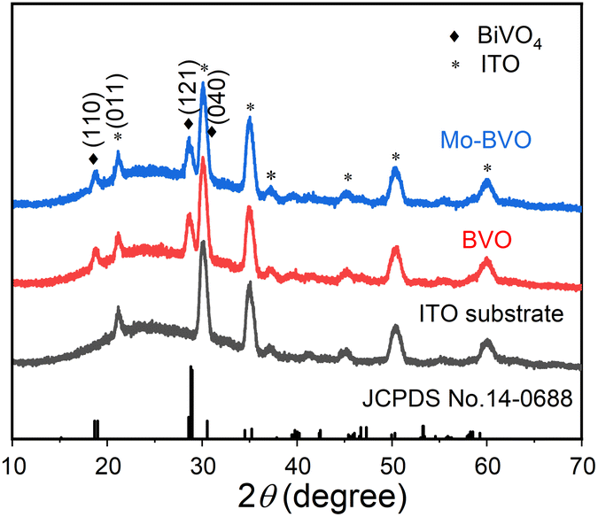 | ||
| Fig. 1 XRD pattern of annealed BVO (red) and Mo-BVO (blue) film samples, ITO substrate was measured as reference. | ||
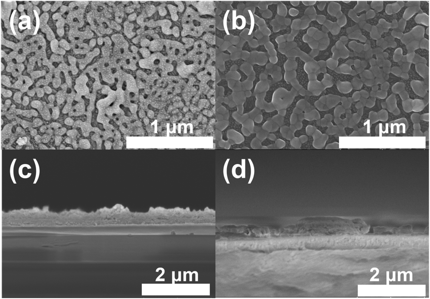 | ||
| Fig. 2 SEM images of BVO (a), Mo-BVO (b) and cross-section of BVO (c) and Mo-BVO (d). | ||
UV-Vis-NIR spectra were recorded to determine the light absorption characteristics of as-prepared BVO samples (Fig. 3(a)). Bare ITO substrate shows an onset of the optical transition energy at 3.0 eV, which does not affect the bandgap determination of BVO samples. Intrinsic BiVO4 is an indirect semiconductor with a bandgap of 2.4 eV, but its direct optical transition occurs only 200 meV above the conduction band minimum (CBM), explaining the high visible light absorption coefficient.21–23 The bandgaps of BVO and Mo-BVO were determined to 2.49 eV and 2.54 eV, respectively. This implies that Mo doping barely affect the optical bandgap of BVO.
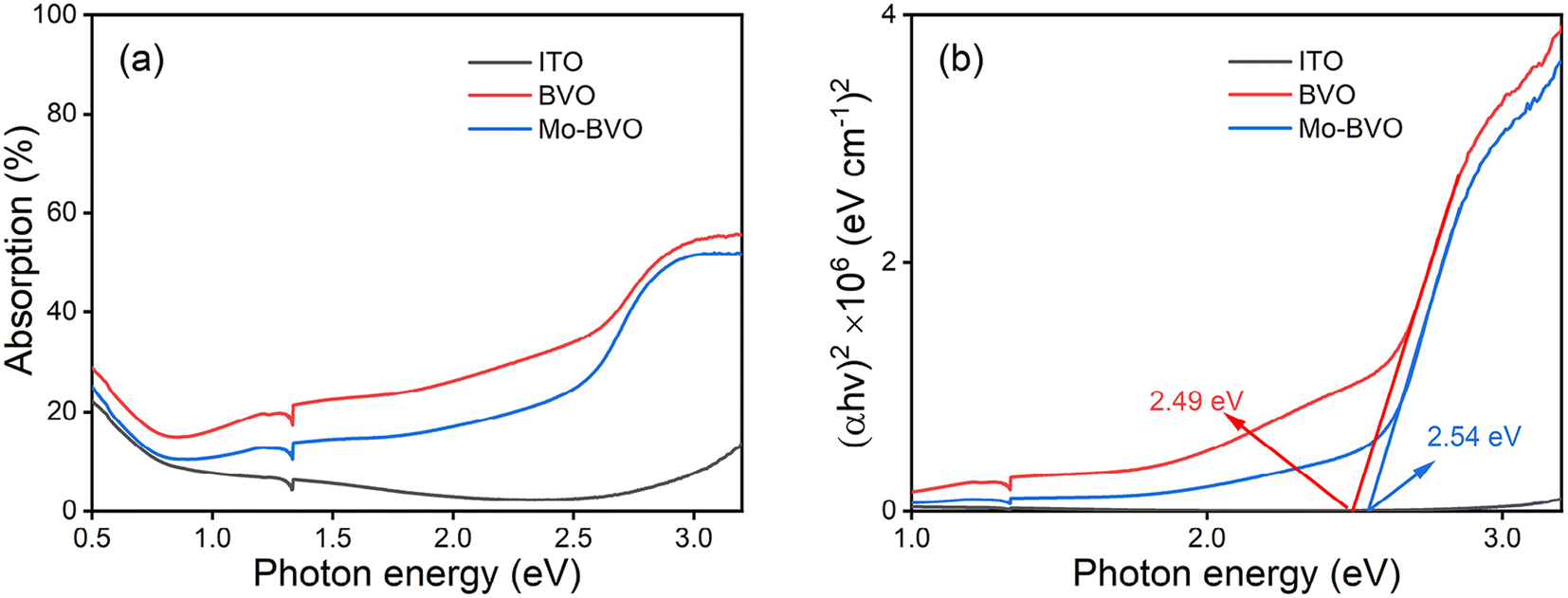 | ||
| Fig. 3 UV-Vis-NIR absorption spectra (a) and corresponding Tauc plots (b) of as-prepared BiVO4 film samples, assuming direct optical absorption. | ||
3.2 Surface analysis of as-prepared BVO samples by X-ray photoemission spectroscopy, specular reflectance FTIR and Raman spectroscopy
To further analyse doping and surface species, X-ray photoemission spectra (XPS) of BiVO4 films were recorded. The emission at a binding energy of 159.0 eV is ascribed to Bi 4f7/2 (Fig. 4(a)).24 The two peaks at 524.2 eV and 516.6 eV are attributed to V 2p1/2 and V 2p3/2, respectively (Fig. 4(b)).25 The binding energies of these states show negligible variation when going from BVO to Mo-BVO. The O 1s emissions located at 529.8 eV, 530.8 eV and 532.5 eV can be ascribed to lattice oxygen, surface –OH groups and adsorbed oxygen species, respectively.15,26,27 Mo 3d3/2 and 3d5/2 states show up at 235.2 eV and 232.1 eV, respectively, indicating that Mo6+ ions are successfully introduced into BiVO4 (Fig. 6(e)).28,29 Additionally, trace N element is observed in BVO and Mo-BVO samples. N 1s binding energy shifts from 400.0 eV of BVO to 398.0 eV of Mo-BVO, implies two kinds of N (Fig. 4(d)). However, peak shifts caused by doping in metal oxides semiconductors are usually small due to limited shifts of the Fermi level. For instance, N 1s binding energy shifts from 400.0 eV to 399.6 eV, when the nitrogen content in N-doped TiO2 increases from 0.5% to 5%.30 Herein, we infer that N originated from Bi(NO3)3 precursor decomposition and only exists at the surface. The four peaks of C 1s at 288.4 eV, 285.5 eV, 284.8 eV and 284.5 eV are assigned to C![[double bond, length as m-dash]](https://www.rsc.org/images/entities/char_e001.gif) O, C–O–C, C–C and CC entities, respectively. The assignment of CO in BVO and Mo-BVO at 288.4 eV mainly originates from adsorbed adventitious carbon. On the other hand, the assignments of C–C in BVO at 284.8 eV and CC in Mo-BVO at 284.5 eV indicate two kinds of carbon species (sp3 and sp2 carbon). Combined with Raman results (see below), we infer that short sp3 carbon chains and short sp2 carbon chains exist on BVO and Mo-BVO, respectively.
O, C–O–C, C–C and CC entities, respectively. The assignment of CO in BVO and Mo-BVO at 288.4 eV mainly originates from adsorbed adventitious carbon. On the other hand, the assignments of C–C in BVO at 284.8 eV and CC in Mo-BVO at 284.5 eV indicate two kinds of carbon species (sp3 and sp2 carbon). Combined with Raman results (see below), we infer that short sp3 carbon chains and short sp2 carbon chains exist on BVO and Mo-BVO, respectively.
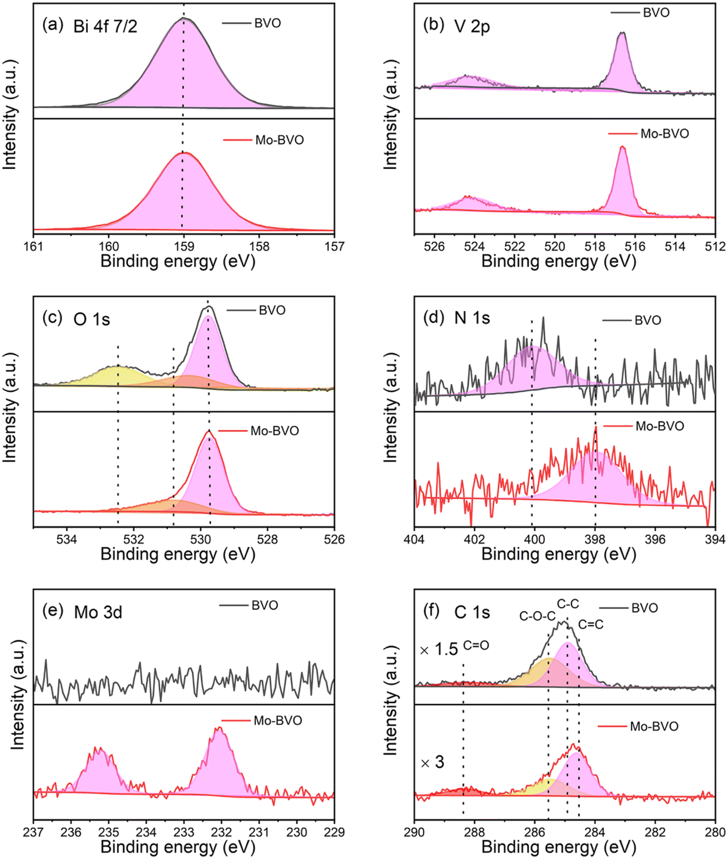 | ||
| Fig. 4 High resolution XPS spectra of Bi 4f7/2 (a), V 2p (b), O 1s (c), N 1s (d), Mo 3d (e) and C 1s (f) of as-prepared BVO samples. | ||
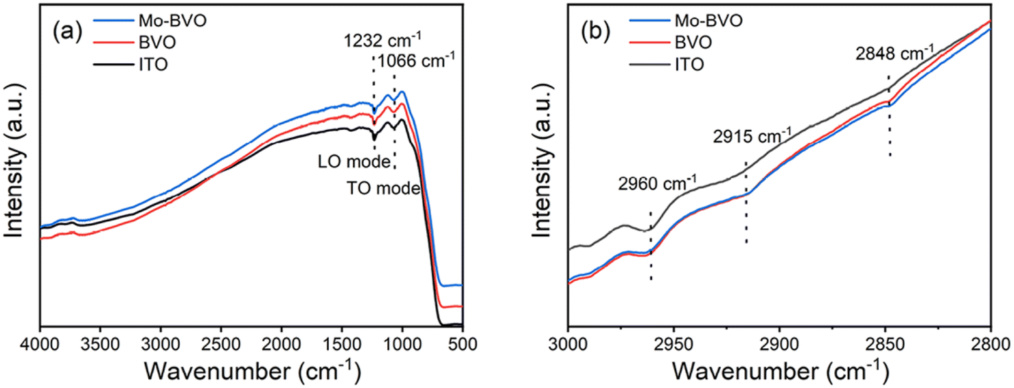
To obtain further insight into the speciation of surface functional groups of as-prepared BVO samples, specular reflectance FTIR spectra were recorded. Characteristic peaks of as-prepared films are displayed in Fig. 5(a). The peaks located at 1232 cm−1 and 1066 cm−1 are ascribed to longitudinal optical (LO) and transversal optical (TO) Si–O–Si vibration mode of ITO glass.31 In the typical C–H stretching vibration ν(C–H) region of 2800–3000 cm−1, 2960 cm−1 is attributed to asymmetric stretching vibration mode of –CH3 functional groups while 2915 cm−1 and 2848 cm−1 are attributed to asymmetric and symmetric stretching of –CH2- groups, respectively.32 As shown in Fig. 5(b), both BVO and Mo-BVO show trace amounts of –CH2- carbon chain species.
 | ||
| Fig. 5 Reflectance FTIR spectra of as-prepared BVO films (a) and enlarged region of 2800–3000 cm−1 (b). | ||
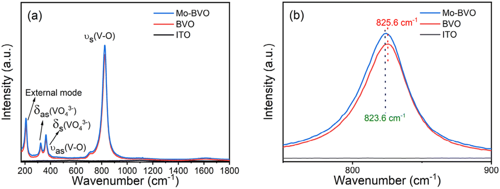
Raman spectra of all samples are presented in Fig. 6(a). The bands located at around 207, 322, 364, 710, 825 cm−1 are attributed to characteristic peaks of monoclinic BiVO4.33,34 The band at 207 cm−1 is assigned to the external mode of VO43− group. The motion frequencies of external modes in polyatomic ions are usually much lower than that of internal modes due to their heavier masses.16 The bands at 322 cm−1 and 364 cm−1 are associated with the asymmetric and symmetric bending vibration modes of the VO43− group, while the bands at 710 cm−1 and 825 cm−1 are attributed to asymmetric and symmetric stretching vibration modes of the V–O bond, respectively. As shown in Fig. 6(b), the main peak of BiVO4 originated from symmetric stretching vibration of V–O band shifts from 825.6 cm−1 to 823.6 cm−1, which is indicative of Mo ions being doped into BiVO4.14
 | ||
| Fig. 6 Raman spectra of as-prepared BVO films (a) and enlarged regions of 750–900 cm−1 (b) and 1000–2000 cm−1. | ||
3.3. Photoelectrochemical measurements
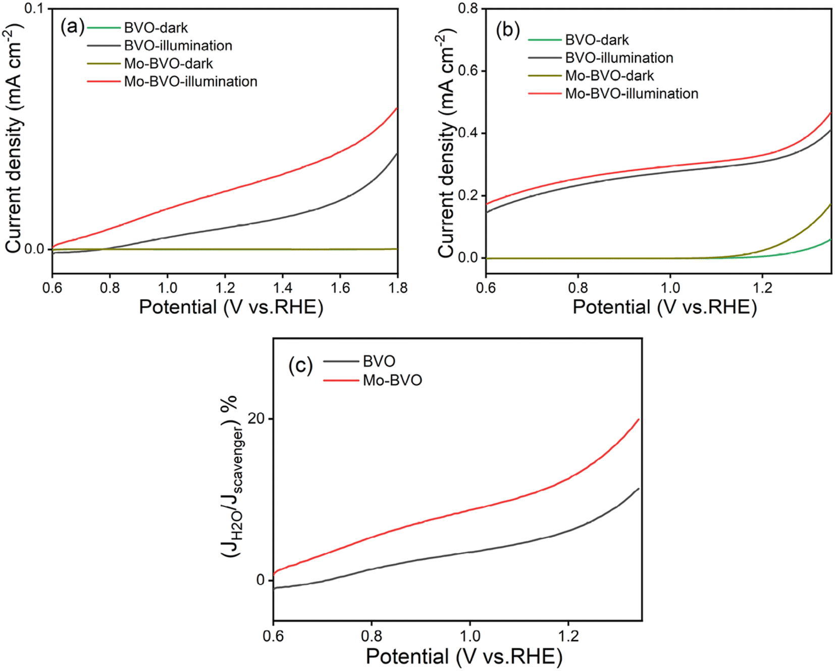 | ||
| Fig. 7 Linear sweep voltammetry (LSV) of as-prepared samples in the dark and under illumination (λexc = 435 nm, 100 mW cm−2), measured in 0.1 M phosphate buffer solution (a) and 0.5 M Na2SO3 solution (b); charge transfer efficiency under illumination, calculated from LSV curves (c). | ||
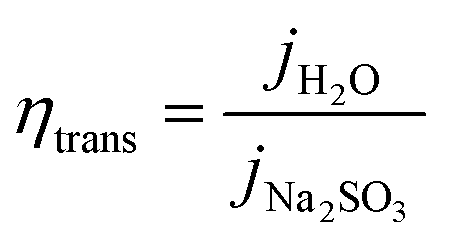
The charge transfer efficiency ηtrans curves of BVO and Mo-BVO can be obtained by using the equation (Fig. 7(c)):
 | (1) |
Charge transfer efficiencies of BVO and Mo-BVO are 6.8% and 13.7%, respectively. It indicates that Mo doping can accelerate charge transfer at the interface by a factor of 2–3.
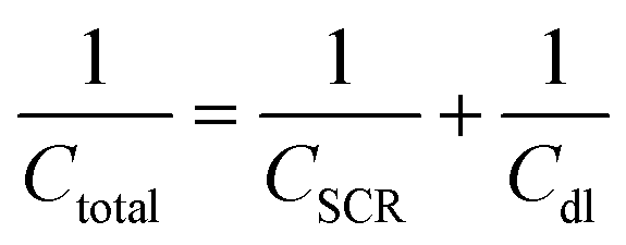 | (2) |
| Rtotal = Rbulk + Rct | (3) |
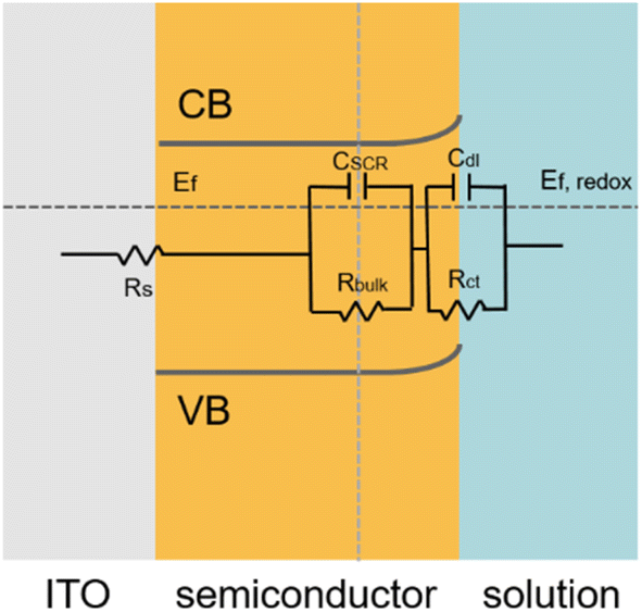 | ||
| Fig. 8 Schematic diagram of semiconductor electrolyte interface. Rs is the solution resistance between working electrode and reference electrode, Rbulk is bulk resistance, CSCR is capacitance of space charge region, Rct is charge transfer resistance, Cdl is capacitance of electric double layer. | ||
Additionally, we assume that charge transfer resistance (Rct) measured in Na2SO3 solution at 1.20 VRHE approximately is zero and bulk resistance is independent of electrolyte. In this case, Rtotal equals to Rct.
The detailed fitting results of the EIS data are summarized in the Fig. S4, Tables S1 and S2.† The total resistances of BVO and Mo-BVO, measured at +1.2 VRHE in 0.1 M phosphate buffer solution in the dark, are 12.6 MΩ and 5.51 MΩ, respectively. This indicates the absence of an oxidation current at 1.2 V vs. RHE, which is consistent with LSV data. Resistances of BVO and Mo-BVO sharply drop to 31.6 kΩ and 19.9 kΩ under illumination. In this case, Rtotal obviously decreases 2–3 orders of magnitude under illumination (Fig. 9(a) and (c)). Therefore, the current density of photoanodes, inversely proportional to Rtotal, is remarkably increased.
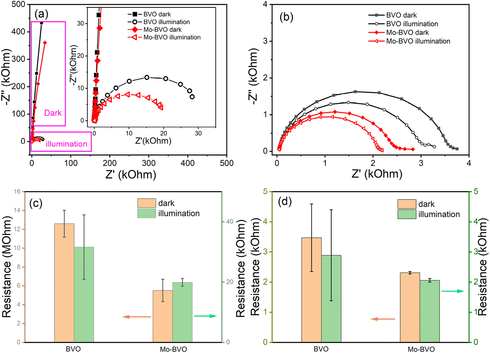 | ||
| Fig. 9 Electrochemical impedance spectra and corresponding interfacial resistances of as-prepared samples in the dark and under illumination (435 nm, 100 mW cm−2), measured in 0.1 M phosphate buffer solution ((a) and (c)) and 0.5 M Na2SO3 solution ((b) and (d)) at the potential of 1.2 V vs. RHE. Error bars originates from repetitive measurements of second samples. | ||
To further calculate the contributions of Rbulk and Rct on the current density, EIS measurements of BVO and Mo-BVO are conducted in 0.5 M Na2SO3 solution at 1.2 V vs. RHE as well. Rbulk of BVO and Mo-BVO slightly decrease from 3.4 kΩ and 2.31 kΩ in the dark to 2.89 kΩ and 2.06 kΩ under illumination, respectively (see Fig. 9(b) and (d)). These decreased resistances originate from increased photoconductivity under illumination.
R ct of OER is thousand times higher than Rbulk in the dark, while Rct of OER is 2.6 to 10 times higher than Rbulk under illumination, which means that both dark current and photocurrent densities of OER are limited by Rct, rather than Rbulk. On the other hand, Mo doping slightly decreases Rbulk but obviously decreases Rct under illumination, which implies that the increase of interface active sites is more important than that of bulk conductivity for photoelectrochemical OER, i.e., bulk concentration of charge carriers.
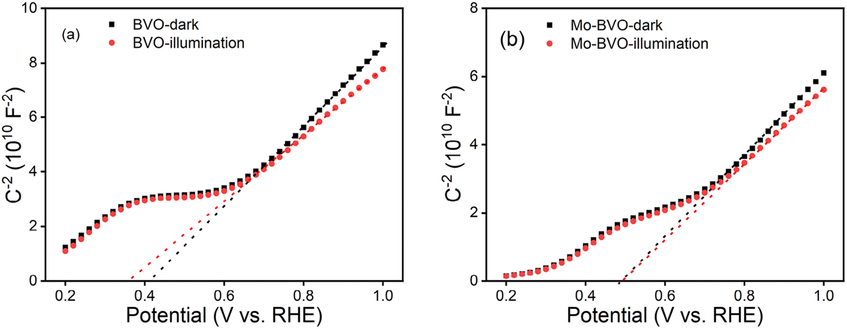 | ||
| Fig. 10 Mott–Schottky plots of BVO (a) and Mo-BVO (b), measured in 0.1 M phosphate buffer solution (pH 6.8) at an applied bias of 1.2 V vs. RHE in the dark and under illumination (435 nm 100 mW cm−2). | ||
The concentrations of charge carriers of BVO and Mo-BVO in the dark were determined to be 1.82 × 1019 cm−3, 2.22 × 1019 cm−3, while the concentrations of charge carriers under illumination were increased to be 2.16 × 1019 cm−3 and 2.46 × 1019 cm−3, according to the following equation.
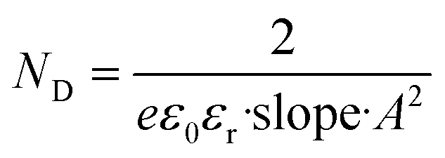 | (4) |
N D is the donor density, e is elementary charge, ε0 is the dielectric constant in vacuum, εr is relative dielectric constant of the material. A is the actual illuminated surface area. The rise in the charge carrier density can be interpreted as an increase of the photoconductivity and thus a reduction of the bulk resistances. The measured flat band potentials, Efb of Mo-BVO, which have found to be at 0.48 V, respectively, showed no changes after illumination. However, the Efb of BVO shifts from 0.41 eV to 0.36 eV (Table 1). This effect is due to trapping of photo-excited holes at surface states.38,39
| Samples | Conditions | E fb (V vs. RHE) | Concentration of charge carriers (cm−3) |
|---|---|---|---|
| BVO | Dark | 0.41 | 1.82 × 10¹⁹ |
| Illumination | 0.36 | 2.16 × 10¹⁹ | |
| Mo-BVO | Dark | 0.48 | 2.22 × 10¹⁹ |
| Illumination | 0.48 | 2.46 × 10¹⁹ |
The presence of surface defect states in the BVO sample is also demonstrated by its low photovoltage as shown in Fig. 11. The photovoltages of BVO and Mo-BVO under illumination (435nm, 100 mW cm−2) are 0.063 eV, 0.216 eV, respectively. It is reported that surface states give rise to Fermi level pinning effects at the solid–electrolyte interface, which obviously limits the photovoltage.40 Because of this, the concentration of photo-generated charge carriers in BVO is much higher than that of Mo-BVO, but the photovoltage of BVO is much lower than that of Mo-BVO (see Fig. 11). Commonly, surface states in BVO arise from V vacancies, so the amount of surface states are reduced after Mo doping into V sites.41
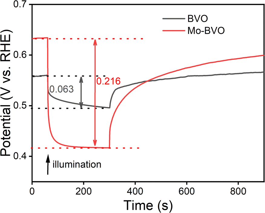 | ||
| Fig. 11 Photovoltage of as-prepared samples under illumination (435 nm, 100 mW cm−2), measured at open circuit potentials in 0.1 M phosphate buffer solution. | ||
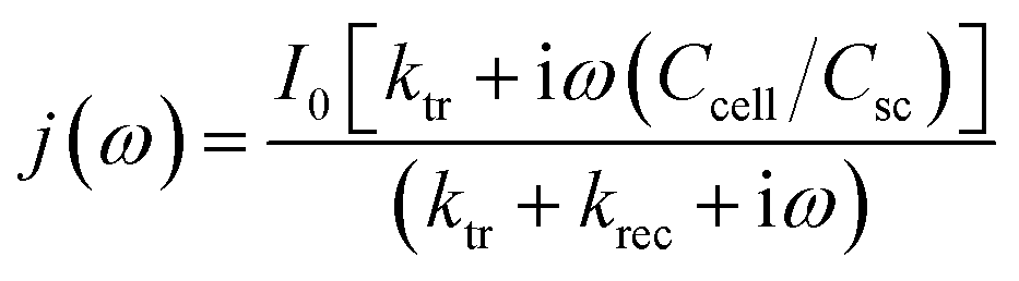
The transfer and recombination kinetics of surface charge carriers of BVO samples are investigated by intensity modulated photocurrent spectroscopy (IMPS) (Fig. 12). The photocurrent can be depicted by the following equation according to Peter's model.42
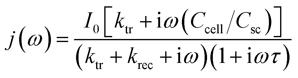 | (5) |
 . Csc and CH are the capacitances of space charge layer and Helmholtz layer. ktr and krec are transfer rate constant and recombination rate constant of photo-generated minority charge carriers, respectively. τ is the time constant of the electrochemical cell38,42
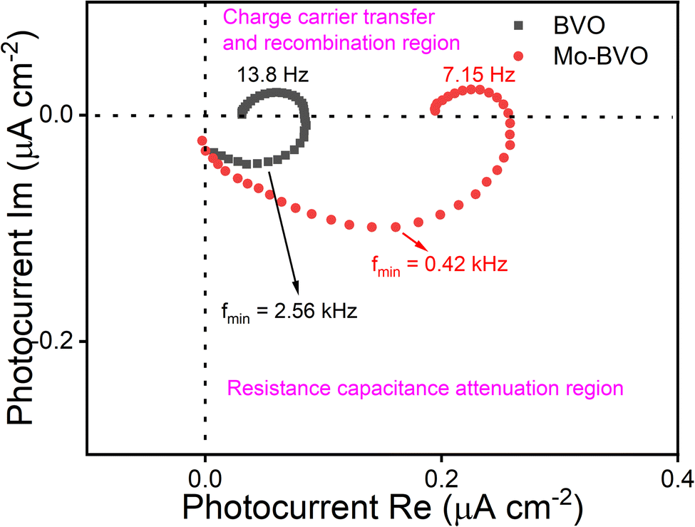 | ||
| Fig. 12 Intensity modulated photocurrent spectroscopy (IMPS) of as-prepared samples under illumination (435 nm 100 mW cm−2), measured at 1.2 V vs. RHE in 0.1 M phosphate buffer solution. | ||
In the case that τ is at least two decades smaller than 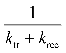 ,43 the above equation can be simplified as follows.
 | (6) |
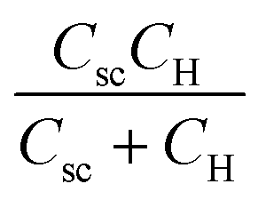
Resistance capacitance (RC) attenuation and competition between charge carrier transfer and recombination usually occur in the 4th and 1st quadrants, respectively.44,45 The angular frequency corresponds to the sum of ktr and krec, when the imaginary part reaches a maximum value in the 1st quadrant, i.e., ωmax = 2πfmax = kt + krec. When the imaginary part is equal to zero, the intercepts of the x axis correspond to 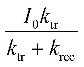 and
and 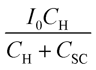 , respectively. Normally, the space charge capacitance is much smaller than the Helmholtz capacitance (Csc ≪ CH). Therefore, the ratio of the x intercepts is equal to
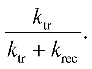
At short circuit conditions, the photo-generated majority charge carriers would migrate to the back layer of the photoanode and recombine with minority charge carriers at the back contact.46 Accordingly, the transit time of electrons reflects their recombination possibility at the back contact and can be obtained from the equation from RC attenuation region.
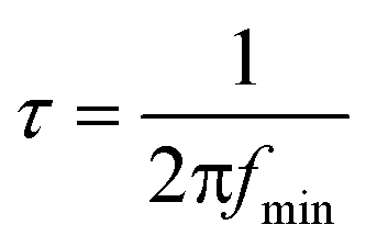 | (7) |
The calculated ktr and krec of photo-excited holes and transit time of photo-generated electrons are summarized in Table 2. The average electron transit times of BVO and Mo-BVO are 0.06 ms and 0.38 ms, respectively, indicating that the photo-generated electrons in BVO transfer much faster, comparing Mo-BVO. This also implies that the PEC water splitting process is limited by the transfer of photo-excited holes, not the photo-excited electrons. The surface recombination rate of Mo-BVO is 5 times lower than that of BVO, verifying that Mo doping can reduce effectively surface recombination of BVO due to an increased amount of surface states.
| Samples | Transfer rate constant of charge carriers ktr (s−1) | Recombination rate constant of charge carriers krec (s−1) | Transit time of electrons τ (ms) |
|---|---|---|---|
| BVO | 31 | 55 | 0.06 |
| Mo-BVO | 34 | 11 | 0.38 |
4. Conclusions
To summarize, the photoelectrochemical activities of semiconductors are closely dependent on their resistance at the semiconductor electrolyte interface. In our study, Mo doping of BVO films was introduced by a spin coating approach. Mo doping are confirmed by XPS and Raman spectra. The influence of Mo doping on BVO is investigated from the aspect of interfacial resistance and charge carrier transfer. Our results show: (1) interfacial charge transfer resistances (Rct) of BiVO4 in 0.1 M phosphate buffer solution decrease 2 to 3 orders of magnitude under illumination. (2) both dark and photo current densities of BVO in OER are dominantly limited by Rct, rather than Rbulk; (3) Mo doping of BVO can not only effectively decrease charge transfer resistance (Rct) under illumination, but also increase photovoltage; (4) in comparison with bare BVO, Mo doped BVO exhibits an enhanced photocurrent density at 1.23 V vs. RHE by a factor of 2.7.Author contributions
Xiaofeng Wu: design, experiments, data analysis & writing – original draft. Freddy E. Oropeza: review & revision. Zheng Qi: SEM measurements and analysis. Marcus Einert: PEC measurements, review and revision. Chuanmu Tian: XRD measurement and analysis. Clément Maheu: XPS measurement and analysis, revision. Kangle Lv: SEM measurements and revision. Jan P. Hofmann: review & editing, conceptualization, supervision.Conflicts of interest
There are no conflicts to declare.Acknowledgements
Xiaofeng Wu and Chuanmu Tian thank for the support of the China Scholarship Council, affiliated to the Ministry of Education of the P.R. of China (Scholarships no. 201708420159 and 202008420222). Marcus Einert acknowledges financial support by the Deutsche Forschungsgemeinschaft (DFG, German Research Foundation, Walter Benjamin Program) under project no. 469377211. Clément Maheu is grateful for financial support from the DFG priority program SPP2196 through project no. 423746744.References
- M. A. Marwat, M. Humayun, M. W. Afridi, H. Zhang, M. R. Abdul Karim, M. Ashtar, M. Usman, S. Waqar, H. Ullah, C. Wang and W. Luo, Advanced Catalysts for Photoelectrochemical Water Splitting, ACS Appl. Energy Mater., 2021, 4, 12007–12031 CrossRef CAS.
- F. Le Formal, E. Pastor, S. D. Tilley, C. A. Mesa, S. R. Pendlebury, M. Gratzel and J. R. Durrant, Rate law analysis of water oxidation on a hematite surface, J. Am. Chem. Soc., 2015, 137, 6629–6637 CrossRef CAS PubMed.
- J. Tang, J. R. Durrant and D. R. Klug, Mechanism of Photocatalytic Water Splitting in TiO2. Reaction of Water with Photoholes, Importance of Charge Carrier Dynamics, and Evidence for Four-Hole Chemistry, J. Am. Chem. Soc., 2008, 130, 13885–13891 CrossRef CAS PubMed.
- K. T. Butler, B. J. Dringoli, L. Zhou, P. M. Rao, A. Walsh and L. V. Titova, Ultrafast carrier dynamics in BiVO4 thin film photoanode material: interplay between free carriers, trapped carriers and low-frequency lattice vibrations, J. Mater. Chem. A, 2016, 4, 18516–18523 RSC.
- F. F. Abdi, T. J. Savenije, M. M. May, B. Dam and R. van de Krol, The Origin of Slow Carrier Transport in BiVO4 Thin Film Photoanodes: A Time-Resolved Microwave Conductivity Study, J. Phys. Chem. Lett., 2013, 4, 2752–2757 CrossRef CAS.
- A. J. Rettie, H. C. Lee, L. G. Marshall, J. F. Lin, C. Capan, J. Lindemuth, J. S. McCloy, J. Zhou, A. J. Bard and C. B. Mullins, Combined charge carrier transport and photoelectrochemical characterization of BiVO4 single crystals: intrinsic behavior of a complex metal oxide, J. Am. Chem. Soc., 2013, 135, 11389–11396 CrossRef CAS PubMed.
- J. H. Kim and J. S. Lee, Elaborately Modified BiVO4 Photoanodes for Solar Water Splitting, Adv. Mater., 2019, 31, 1806938 CrossRef PubMed.
- F. F. Abdi, L. Han, A. H. Smets, M. Zeman, B. Dam and R. van de Krol, Efficient solar water splitting by enhanced charge separation in a bismuth vanadate-silicon tandem photoelectrode, Nat. Commun., 2013, 4, 2195 CrossRef PubMed.
- M. Schleuning, M. Kölbach, F. F. Abdi, K. Schwarzburg, M. Stolterfoht, R. Eichberger, R. van de Krol, D. Friedrich and H. Hempel, Generalized Method to Extract Carrier Diffusion Length from Photoconductivity Transients: Cases of BiVO4, Halide Perovskites, and Amorphous and Crystalline Silicon, PRX Energy, 2022, 1, 023008 CrossRef.
- F. F. Abdi and R. van de Krol, Nature and Light Dependence of Bulk Recombination in Co-Pi-Catalyzed BiVO4 Photoanodes, J. Phys. Chem. C, 2012, 116, 9398–9404 CrossRef CAS.
- R. G. Li, F. X. Zhang, D. E. Wang, J. X. Yang, M. R. Li, J. Zhu, X. Zhou, H. X. Han and C. Li, Spatial separation of photogenerated electrons and holes among {010} and {110} crystal facets of BiVO4, Nat. Commun., 2013, 4, 1432 CrossRef PubMed.
- S. S. Patil, M. G. Mali, M. A. Hassan, D. R. Patil, S. S. Kolekar and S. W. Ryu, One-Pot in Situ Hydrothermal Growth of BiVO4/Ag/rGO Hybrid Architectures for Solar Water Splitting and Environmental Remediation, Sci. Rep., 2017, 7, 8404 CrossRef PubMed.
- W. Kim and K.-S. Choi, Nanoporous BiVO4 Photoanodes with Dual-Layer Oxygen Evolution Catalysts for Solar Water Splitting, Science, 2014, 343, 990–994 CrossRef PubMed.
- X. Zhao, W. Luo, J. Feng, M. Li, Z. Li, T. Yu and Z. Zou, Quantitative Analysis and Visualized Evidence for High Charge Separation Efficiency in a Solid-Liquid Bulk Heterojunction, Adv. Energy Mater., 2014, 4, 1301785 CrossRef.
- Z. Jiang, Y. Liu, T. Jing, B. Huang, X. Zhang, X. Qin, Y. Dai and M.-H. Whangbo, Enhancing the Photocatalytic Activity of BiVO4 for Oxygen Evolution by Ce Doping: Ce3+ Ions as Hole Traps, J. Phys. Chem. C, 2016, 120, 2058–2063 CrossRef CAS.
- W. Luo, J. Wang, X. Zhao, Z. Zhao, Z. Li and Z. Zou, Formation energy and photoelectrochemical properties of BiVO4 after doping at Bi3+ or V5+ sites with higher valence metal ions, Phys. Chem. Chem. Phys., 2013, 15, 1006–1013 RSC.
- J. H. Yang, D. E. Wang, H. X. Han and C. Li, Roles of Cocatalysts in Photocatalysis and Photoelectrocatalysis, Acc. Chem. Res., 2013, 46, 1900–1909 CrossRef CAS PubMed.
- D. Wang, R. Li, J. Zhu, J. Shi, J. Han, X. Zong and C. Li, Photocatalytic Water Oxidation on BiVO4 with the Electrocatalyst as an Oxidation Cocatalyst: Essential Relations between Electrocatalyst and Photocatalyst, J. Phys. Chem. C, 2012, 116, 5082–5089 CrossRef CAS.
- X. X. Chang, T. Wang, P. Zhang, J. J. Zhang, A. Li and J. L. Gong, Enhanced Surface Reaction Kinetics and Charge Separation of p–n Heterojunction Co3O4/BiVO4 Photoanodes, J. Am. Chem. Soc., 2015, 137, 8356–8359 CrossRef CAS PubMed.
- W. Luo, Z. Yang, Z. Li, J. Zhang, J. Liu, Z. Zhao, Z. Wang, S. Yan, T. Yu and Z. Zou, Solar hydrogen generation from seawater with a modified BiVO4 photoanode, Energy Environ. Sci., 2011, 4, 4046–4051 RSC.
- M. V. Malashchonak, E. A. Streltsov, D. A. Kuliomin, A. I. Kulak and A. V. Mazanik, Monoclinic bismuth vanadate band gap determination by photoelectrochemical spectroscopy, Mater. Chem. Phys., 2017, 201, 189–193 CrossRef CAS.
- J. K. Cooper, S. Gul, F. M. Toma, L. Chen, P.-A. Glans, J. Guo, J. W. Ager, J. Yano and I. D. Sharp, Electronic Structure of Monoclinic BiVO4, Chem. Mater., 2014, 26, 5365–5373 CrossRef CAS.
- J. K. Cooper, S. Gul, F. M. Toma, L. Chen, Y.-S. Liu, J. Guo, J. W. Ager, J. Yano and I. D. Sharp, Indirect Bandgap and Optical Properties of Monoclinic Bismuth Vanadate, J. Phys. Chem. C, 2015, 119, 2969–2974 CrossRef CAS.
- Y. Wei, J. Su, X. Wan, L. Guo and L. Vayssieres, Spontaneous photoelectric field-enhancement effect prompts the low cost hierarchical growth of highly ordered heteronanostructures for solar water splitting, Nano Res., 2016, 9, 1561–1569 CrossRef CAS.
- T. Jiang, F. Nan and J. Zhou, Enhanced photocatalytic and photoelectrochemical performance of g-C3N4/BiVO4 heterojunction: A combined experimental and theoretical study, AIP Adv., 2019, 9, 055225 CrossRef.
- Y. Zhou, L. Zhang, L. Lin, B. R. Wygant, Y. Liu, Y. Zhu, Y. Zheng, C. B. Mullins, Y. Zhao, X. Zhang and G. Yu, Highly Efficient Photoelectrochemical Water Splitting from Hierarchical WO3/BiVO4 Nanoporous Sphere Arrays, Nano Lett., 2017, 17, 8012–8017 CrossRef CAS PubMed.
- S. Wang, P. Chen, Y. Bai, J. H. Yun, G. Liu and L. Wang, New BiVO4 Dual Photoanodes with Enriched Oxygen Vacancies for Efficient Solar-Driven Water Splitting, Adv. Mater., 2018, 30, 1800486 CrossRef PubMed.
- W. Ji, R. Shen, R. Yang, G. Yu, X. Guo, L. Peng and W. Ding, Partially nitrided molybdenum trioxide with promoted performance as an anode material for lithium-ion batteries, J. Mater. Chem. A, 2014, 2, 699–704 RSC.
- S. Durairaj, P. Krishnamoorthy, N. Raveendran, B. D. Ryu, C.-H. Hong, T. H. Seo and S. Chandramohan, Barrier-assisted vapor phase CVD of large-area MoS2 monolayers with high spatial homogeneity, Nanoscale Adv., 2020, 2, 4106–4116 RSC.
- J. Feng, W. Bao, L. Li, H. Cheng, W. Huang, H. Kong and Y. Li, The synergistic effect of nitrogen-doped titanium dioxide/mercaptobenzoic acid/silver nanocomplexes for surface-enhanced Raman scattering, J. Nanopart. Res., 2018, 20, 82 CrossRef.
- S. H. Brewer and S. Franzen, Optical properties of indium tin oxide and fluorine-doped tin oxide surfaces: correlation of reflectivity, skin depth, and plasmon frequency with conductivity, J. Alloys Compd., 2002, 338, 73–79 CrossRef CAS.
- R. Lu, W. Gan, B.-H. Wu, Z. Zhang, Y. Guo and H.-F. Wang, C-H Stretching Vibrations of Methyl, Methylene and Methine Groups at the Vapor/Alcohol (n = 1–8) Interfaces, J. Phys. Chem. B, 2005, 109, 14118–14129 CrossRef CAS PubMed.
- V.-I. Merupo, S. Velumani, K. Ordon, N. Errien, J. Szade and A.-H. Kassiba, Structural and optical characterization of ball-milled copper-doped bismuth vanadium oxide (BiVO4), CrystEngComm, 2015, 17, 3366–3375 RSC.
- M. R. d. S. Pelissari, N. F. Azevedo Neto, L. P. Camargo and L. H. Dall'Antonia, Characterization and Photo-Induced Electrocatalytic Evaluation for BiVO4 Films Obtained by the SILAR Process, Electrocatalysis, 2021, 12, 211–224 CrossRef CAS.
- K. J. McDonald and K.-S. Choi, A new electrochemical synthesis route for a BiOI electrode and its conversion to a highly efficient porous BiVO4 photoanode for solar water oxidation, Energy Environ. Sci., 2012, 5, 8553 RSC.
- J. Gu, Q. Huang, Y. Yuan, K.-H. Ye, Z. Wang and W. Mai, In situ growth of a TiO2 layer on a flexible Ti substrate targeting the interface recombination issue of BiVO4 photoanodes for efficient solar water splitting, J. Mater. Chem. A, 2017, 5, 20195–20201 RSC.
- X. Wan, F. Niu, J. Su and L. Guo, Enhanced photoelectrochemical water oxidation of bismuth vanadate via a combined strategy of W doping and surface RGO modification, Phys. Chem. Chem. Phys., 2016, 18, 31803–31810 RSC.
- M. Antuch, P. Millet, A. Iwase and A. Kudo, The role of surface states during photocurrent switching: Intensity modulated photocurrent spectroscopy analysis of BiVO4 photoelectrodes, Appl. Catal., B, 2018, 237, 401–408 CrossRef CAS.
- S. K. Mohapatra, S. E. John, S. Banerjee and M. Misra, Water Photooxidation by Smooth and Ultrathin α-Fe2O3 Nanotube Arrays, Chem. Mater., 2009, 21, 3048–3055 CrossRef CAS.
- B. J. Trześniewski and W. A. Smith, Photocharged BiVO4 photoanodes for improved solar water splitting, J. Mater. Chem. A, 2016, 4, 2919–2926 RSC.
- M. Lamers, S. Fiechter, D. Friedrich, F. F. Abdi and R. van de Krol, Formation and suppression of defects during heat treatment of BiVO4 photoanodes for solar water splitting, J. Mater. Chem. A, 2018, 6, 18694–18700 RSC.
- E. A. Ponomarev and L. M. Peter, A generalized theory of intensity modulated photocurrent spectroscopy (IMPS), J. Electroanal. Chem., 1995, 396, 219–226 CrossRef.
- H. Cachet and E. M. M. Sutter, Kinetics of Water Oxidation at TiO2 Nanotube Arrays at Different pH Domains Investigated by Electrochemical and Light-Modulated Impedance Spectroscopy, J. Phys. Chem. C, 2015, 119, 25548–25558 CrossRef CAS.
- F. Li, H. Yang, Q. Zhuo, D. Zhou, X. Wu, P. Zhang, Z. Yao and L. Sun, ACobalt@Cucurbit[5]uril Complexasa Highly Efficient Supra-molecular Catalyst for Electrochemical and Photoelectrochemical Water Splitting, Angew. Chem., Int. Ed., 2021, 60, 1976–1985 CrossRef CAS PubMed.
- B. Gao, T. Wang, X. Fan, H. Gong, P. Li, Y. Feng, X. Huang, J. He and J. Ye, Enhanced water oxidation reaction kinetics on a BiVO4 photoanode by surface modification with Ni4O4 cubane, J. Mater. Chem. A, 2019, 7, 278–288 RSC.
- L. Xia, J. Li, J. Bai, L. Li, Q. Zeng, Q. Xu and B. Zhou, Preparation of a BiVO4 nanoporous photoanode based on peroxovanadate reduction and conversion for efficient photoelectrochemical performance, Nanoscale, 2018, 10, 2848–2855 RSC.
Footnote |
| † Electronic supplementary information (ESI) available. See DOI: https://doi.org/10.1039/d3se00061c |
| This journal is © The Royal Society of Chemistry 2023 |