
 Open Access Article
 This Open Access Article is licensed under a Creative Commons Attribution-Non Commercial 3.0 Unported Licence
Highly transparent Bi4Ti3O12 thin-film electrodes for ferroelectric-enhanced photoelectrochemical processes†
Simone
Casadio
 ab,
Angela
Gondolini
a,
Nicola
Sangiorgi
a,
Andrea
Candini
c and
Alessandra
Sanson
*a
ab,
Angela
Gondolini
a,
Nicola
Sangiorgi
a,
Andrea
Candini
c and
Alessandra
Sanson
*a
aInstitute of Science and Technology for Ceramics (ISTEC) of the National Research Council (CNR), Via Granarolo 64, 48018 Faenza, RA, Italy. E-mail: alessandra.sanson@istec.cnr.it
bDepartment of Chemical Sciences, Università degli Studi di Padova, Via Marzolo 1, 35131 Padova, Italy
cInstitute for Organic Synthesis and Photoreactivity (ISOF) of the National Research Council (CNR), Via Gobetti 101, 40129 Bologna, Italy
First published on 13th December 2022
Abstract
In a photo-electrochemical (PEC) cell, rapid spatial separation of the photo-generated carriers and their transport kinetics within the photo-electrode materials are fundamental to achieving high-performance devices and avoiding charge recombination. Recently the use of ferroelectric potential in ferroelectric photo-active semiconductors has shown to be an effective strategy to modulate the charge transfer properties both in the bulk phase and at the surface of semiconductors. In this perspective, the Aurivillius perovskite Bi4Ti3O12 (BiTO) is of great interest owing to its excellent photocatalytic activity and strong spontaneous ferroelectric polarization. The use of BiTO powder for the photocatalytic reduction of CO2 has recently been reported, but its utilization as a photo-electrode for the photo-electrochemical (PEC) reduction of carbon dioxide has never been exploited, especially assisted by a ferroelectric potential. In this work, highly transparent BiTO-based thin film photo-cathodes were fabricated via a sol–gel/spin coating coupled process and optimized, for the first time in the literature, for CO2 PEC reduction. The influence of the number of depositions on the photo-electrochemical properties was initially accurately investigated and an optimized photo-electrode was thus obtained, which registered a maximum current density of −4.1 mA cm2 under illumination conditions. In addition, the effect of the ferroelectric potential on the photo-electrochemical performances was accurately studied in this optimized system producing a current density increment of about 50% and an enhanced charge transfer ability, thus demonstrating the possibility of effectively adopting ferroelectric polarization in BiTO photo-electrodes to boost the photo-electrochemical reduction of CO2.
1 Introduction
The depletion of fossil fuels caused by the rapid development of industry, the consequent climate changes generated by high carbon dioxide (CO2) emissions, and the energy shortage of our age are matters of major concern in modern society. In this perspective, photocatalytic and photo-electrocatalytic reduction of CO2 can provide an effective and environmentally friendly strategy to address these issues, using solar energy to transform CO2 into clean and valuable fuels and chemicals.1,2 The development of efficient photocatalytic systems has therefore become of great urgency and a hot topic among the scientific community.In recent years, bismuth-based photocatalysts have received increasing attention in the photocatalytic field, due to their appropriate bandgap and tunable surface structure, also achieving excellent results in the photocatalytic reduction of CO2; however, their performances are still limited by the fast charge carrier recombination,3,4 which is a major aspect to be considered and reduced to develop a high-performance photocatalyst.
Among the available bismuth-based photocatalysts, bismuth titanate Bi4Ti3O12 (BiTO) has recently drawn growing interest as an abundant, stable, and highly photocatalytic-active compound,5 due to its peculiar crystal and electron structure.6 Being part of the Aurivillius perovskite family, it possesses in fact a layered crystal structure made up of pseudo-perovskite [Bi2Ti3O10]2− layers composed of three TiO6 octahedral units, which are sandwiched between [Bi2O2]2+ layers along the c-axis. As verified by first-principles calculation,7 in the electronic structure, the hybridized O 2p, and Bi 6s orbitals co-participate in the formation of the valence band. This interaction between Bi and O primarily promotes the migration of photo-generated holes to [Bi2O2]2+, and the electron transfer to the Ti–O octahedral layers so that electrons and holes preferentially move within different areas of the BiTO structure. The effective separation of the photogenerated carriers is therefore achieved in the local unit cell.8 On this basis, several BiTO-based powder systems have been successfully reported over the years, for multiple photocatalytic purposes,9–19 and recently BiTO has been employed as a catalyst also in the CO2 photo-reduction reaction, producing CO,20–24 methanol (CH3OH),21 and methane (CH4).24 In addition to these already promising photocatalytic performances, the distortion of the TiO6 octahedra in the pseudo-perovskite blocks is responsible for the BiTO well-known ferroelectric behavior,25 which has been proven to represent a strong driving force for bulk charge separation.14,26,27 Recently the exploitation of piezo/ferro-electric potentials in photoactive semiconductors has been adopted as an effective strategy to modulate the charge transfer properties both in the bulk phase and at the surface of semiconductors,28,29 and has been also only recently applied to BiTO CO2 photoreduction, employing corona poling on BiTO nanoflowers to enhance the ferroelectric behavior of the material, achieving a 9-times improved CO production rate.30
Besides photocatalysis, adopting ferroelectric semiconductors can be particularly effective in photoelectrochemical (PEC) cells as photoelectrode materials, considering the possibility to modify cell efficiency towards the desired reaction by simply polarizing the photoelectrode, thus representing a great operational advantage.
A lot of work has been published on the study and development of poled ferroelectric photoelectrodes such as BiFeO3,31–40 BaTiO3,41–45 Li/Na/K-NbO3,45–49 PbTiO3–PbZrTiO3,50–53 and SrTiO3,54,55 for the PEC water-splitting reaction, but the use of ferroelectric photocathodes for CO2 PEC reduction has not been exploited yet. On the other hand, some studies on the production of BiTO ferroelectric layers have been reported for photovoltaic applications,56–58 and only one preliminary work on photo-electrocatalysis has been reported, where thin film BiOI/BiTO electrodes were fabricated via a metering rod method for the photo-electrochemical characterization of this heterostructure, as a photoanode in the ferroelectric-assisted water-splitting reaction.59 Therefore, to the author's best knowledge, this is the first time in the literature that BiTO thin-film photocathodes have been developed for the photoelectrochemical reduction of CO2, and that the possibility to apply a ferroelectric potential to BiTO photoelectrodes has been studied in detail for the ferroelectric-enhanced photoelectrochemical reduction of carbon dioxide.
In this work, highly transparent BiTO thin films were fabricated via a facile sol–gel/spin-coating process to be used as photocathodes for the PEC reduction of carbon dioxide assisted by a ferroelectric potential. The influence of the number of depositions (i.e., amount of photoactive material) on the photo-electrochemical properties was at first accurately investigated and an optimal number of spin-coating cycles was thus identified. The effect of ferroelectric polarization on the photoelectrochemical performances of the optimized electrode was then assessed, showing a remarkable enhancement of the PEC performances in terms of produced electric current and surface charge transfer ability under optimal electric poling conditions. According to the observed results, an explanation of the improved performances was provided based on the material band bending at the electrode/electrolyte interface induced by the ferroelectric potential coupled with the applied external potential. This work, therefore, demonstrates the possibility of effectively adopting a ferroelectric polarization to modulate the PEC performances of BiTO photocathodes in the ferroelectric-assisted CO2 photo-electrochemical reduction.
2 Experimental
2.1 Fabrication of the BiTO photo-electrodes
Thin-film BiTO photocathodes of 2.25 cm2 were fabricated via a sol–gel/spin coating coupled process on FTO substrates (fluorine doped tin oxides, SnO2![[thin space (1/6-em)]](https://www.rsc.org/images/entities/char_2009.gif) :F, Sigma Aldrich, Germany, surface resistivity ∼7 Ω sq−1), in line with previously reported methodologies60,61 (Fig. 1). The BiTO precursor solution was prepared by dissolving a stoichiometric amount of bismuth nitrate [Bi(NO3)3·5H2O] (ACS reagent ≥98.0%, Sigma Aldrich, Germany) in a mixed solution of acetic acid (AcOH) and 2-methoxyethanol (2-MOE) at 1:1 v/v. The resulting solution was stirred at 70 °C for 1 hour under reflux conditions. A second solution was prepared by slowly adding titanium isopropoxide [Ti(OC3H7)4] (Ti-i-PrO4) (≥97.0%, Sigma Aldrich, Germany) under continuous stirring into a 2-MOE solution containing acetylacetone (AcAcH) (≥99.5%, Fluka Analytical, Germany) as a stabilizer to control the rate of hydrolysis and condensation of titanium alkoxide. The as-produced Ti-solution was then added to the Bi-solution and the obtained mixed yellow system was stirred for 2 hours at 70 °C under reflux. Finally, 2-MOE was added to adjust the concentration to 0.02 mol L−1, with a proportion of AcOH and 2-MOE equal to 1:3 v/v. The as-prepared solution was spin-coated using a commercial spin-coater (POLOS Spin 150i-NPP, SPS Europe) onto FTO-coated glass previously sonicated in isopropyl alcohol for 10 min and then rinsed with distilled water. The spin-coating cycle was optimized and set to 1000 rpm for 5 s and 3000 rpm for 25 s, followed by a drying process at 150 °C for 5 min in a static oven to evaporate the solvents. These processes were repeated multiple times to obtain multilayer photoelectrodes (i.e., 3, 5, and 7 depositions), which were then annealed in air at 250 °C and 500 °C for 30 min to allow the formation of the crystal phase.
:F, Sigma Aldrich, Germany, surface resistivity ∼7 Ω sq−1), in line with previously reported methodologies60,61 (Fig. 1). The BiTO precursor solution was prepared by dissolving a stoichiometric amount of bismuth nitrate [Bi(NO3)3·5H2O] (ACS reagent ≥98.0%, Sigma Aldrich, Germany) in a mixed solution of acetic acid (AcOH) and 2-methoxyethanol (2-MOE) at 1:1 v/v. The resulting solution was stirred at 70 °C for 1 hour under reflux conditions. A second solution was prepared by slowly adding titanium isopropoxide [Ti(OC3H7)4] (Ti-i-PrO4) (≥97.0%, Sigma Aldrich, Germany) under continuous stirring into a 2-MOE solution containing acetylacetone (AcAcH) (≥99.5%, Fluka Analytical, Germany) as a stabilizer to control the rate of hydrolysis and condensation of titanium alkoxide. The as-produced Ti-solution was then added to the Bi-solution and the obtained mixed yellow system was stirred for 2 hours at 70 °C under reflux. Finally, 2-MOE was added to adjust the concentration to 0.02 mol L−1, with a proportion of AcOH and 2-MOE equal to 1:3 v/v. The as-prepared solution was spin-coated using a commercial spin-coater (POLOS Spin 150i-NPP, SPS Europe) onto FTO-coated glass previously sonicated in isopropyl alcohol for 10 min and then rinsed with distilled water. The spin-coating cycle was optimized and set to 1000 rpm for 5 s and 3000 rpm for 25 s, followed by a drying process at 150 °C for 5 min in a static oven to evaporate the solvents. These processes were repeated multiple times to obtain multilayer photoelectrodes (i.e., 3, 5, and 7 depositions), which were then annealed in air at 250 °C and 500 °C for 30 min to allow the formation of the crystal phase.
 | ||
| Fig. 1 Schematic representation of the fabrication process of the BiTO multi-layered electrodes. | ||
In this work, seven depositions were chosen as the maximum number of consecutive spin-coating cycles to ensure the fabrication of defect-free thin-film BiTO electrodes (i.e., high uniformity of the coating).
2.2 Structural and morphological characterization
X-ray diffraction (XRD) spectra were collected in variable temperature in situ mode on the BiTO dried precursor, and at room temperature on the BiTO powder sample (i.e., BiTO dried and annealed precursor) and layers on a Bruker D8 Discover advanced diffractometer (Cu Kα1,2, Bruker AXS GmbH, Karlsruhe, Germany) in the 2-theta range 20–70°, to monitor the Bi4Ti3O12 phase evolution, and verify the purity of the obtained crystal phase. Thermal analysis (STA 449 C Jupiter thermo-microbalance, Netzsch-Gerätebau GmbH, 25 – 700 °C, 5 °C min−1, and Air/5% Ar protective gas) of the precursor solution after solvent evaporation was conducted for the determination of an appropriate thermal annealing profile and temperatures (ESI, Section S2†). Morphology analyses were performed via scanning electron microscopy (FE-SEM, FEG-SEM Σigma: Zeiss, Germany) to verify the presence of uniform coatings. FE-SEM cross-sectional images were collected to determine the thickness of the optimized BiTO multi-layered electrode. To assess the surface topography, atomic force microscopy (AFM) analyses were performed in tapping mode with a Bruker MultiMode 8 system using commercial Bruker RTESPA probes (f0 = 300 KHz and k = 40 N m). Raw AFM data were flattened to remove experimental artifacts with SPIP software (https://www.digitalsurf.com/), which was also used to analyze the images calculating the roughness. For each sample, several areas in different positions were probed for a total scanned area larger than 100 μm2 and the average roughness was extracted.2.3 Optical characterization of the BiTO electrodes
Spectrophotometric determination of the film bandgap (Eg) was performed using the absorption spectra recorded in transmission mode using a PVE300 system (Bentham Instruments Ltd, United Kingdom) and applying the Tauc equation.2.4 Electrochemical and photoelectrochemical characterization of the BiTO photoelectrodes
The photoelectrodes were finally characterized from an electrochemical point of view (Autolab PGSTAT302N + FRA32M, Metrohm, Nederland) under dark conditions and under controlled illumination (Solar Simulator ABET Technologies Sun 2000, Connecticut, 1 sun, AM 1.5, 100 mW cm−2). All PEC measurements were performed in a three-electrode cell configuration, using the BiTO films as working electrodes, a platinum wire as the counter electrode, and a silver chloride electrode (Ag/AgCl, 3.0 M KCl) as the reference electrode. Electrochemical impedance spectroscopy (EIS) measurements and Mott–Schottky analyses (MS) of BiTO electrodes with different thicknesses were performed in a 0.1 M KCl aqueous solution (Sigma Aldrich) at −1.2 V (vs. Ag/AgCl) and in the potential window −1.5–0.1 V (vs. Ag/AgCl), (frequency range: 104 to 0.5 Hz) respectively. Linear sweep voltammetry (LSV) was performed under reduction conditions (10 mV s−1, potential window: −1.5 –0.2 V vs. Ag/AgCl) in a 0.1 M KHCO3 aqueous solution (Sigma Aldrich) saturated with CO2 (99.998%, 20 min, and 0.5 L min−1). In addition, EIS measurements were conducted in the same electrolyte (CO2 saturated 0.1 M KHCO3) for the best performing BiTO electrode together with transient photocurrent measurement (J–t) with a frequency of 0.1 Hz. Finally, the whole recorded data were elaborated using Nova 1.12 software. The EIS analyses were fitted by using Z-View software (Scribner Associates). The poling treatment was performed in a two-electrode cell configuration, which operated with the BiTO thin-film electrode as the working electrode and using a platinum plate as the counter electrode in a 0.1 M LiClO4 (Sigma Aldrich) propylene carbonate solution because of the wide electrochemical window33 by applying a bias of ±4 V for 10 seconds. During the poling procedure, the current was kept below 1 mA. In the characterization of the photo-cathodes, to confirm the evolution of hydrogen (i.e., water reduction reaction), which is thermodynamically favored at more negative potentials, chronoamperometry reactions were carried out at the constant voltages of −0.9, −1.2, and −1.4 V vs. Ag/AgCl in the three-electrode configuration previously described for 1 h. Gas samples were analyzed using a 990 micro-GC (Agilent Technologies) equipped with a molecular sieve 5 Å packed column for hydrogen detection and a thermal conductivity detector (TCD); argon was used as the carrier gas.3 Results and discussion
3.1 Structural and morphological characterization
Fig. 2 shows the XRD spectra of the BiTO powder sample obtained by thermally treating the sol–gel precursor according to the described annealing profile (reported in the Experimental part), and of the BiTO spin-coated layer onto FTO-coated glass. | ||
| Fig. 2 XRD patterns of the BiTO powder calcinated at 500 °C (a), the FTO substrate (b), and the spin-coated BiTO film on FTO-coated glass (c). | ||
The obtainment of the orthorhombic Bi4Ti3O12 phase (PDF# 35-0795) was verified in the powder sample with the presence of low-intensity extra peaks (2-theta: 34° and 49°, marked with asterisks) probably attributable to the intermediate pyrochlore phase Bi2Ti2O7 (PDF# 01-074-4250). This phase, which has often been observed both in Bi4Ti3O12 powder samples and films62–64 depending on the synthesis temperature, Bi:Ti molar ratio, substrate, and film growth conditions, has been proven to decompose at temperatures higher than 600 °C (ESI, Fig. S1†), in accordance with the literature.65 However, such heating conditions cannot be employed in the fabrication of the BiTO layers due to the use of FTO-coated glass substrates (ESI, Section S1†). As is shown, because of the thin nature of the deposited layers, in the spin-coated samples FTO peaks are predominant in intensity compared to the BiTO ones, and secondary phases could not be detected.
Spin-coated electrodes with a different number of depositions, namely 3 (BiTO 3), 5 (BiTO 5) and 7 (BiTO 7) depositions, were therefore prepared and fully characterized from a morphological point of view. The number of depositions is in fact a key parameter to be considered for the development of an optimized highly transparent photoelectrode because it is strictly related to the amount of loaded photo-active electrocatalyst and to the transparency of the photoelectrode itself. An increase in the number of depositions affects the film thickness usually leading to increased absorption of light and photocurrent. Nevertheless, this increment has been observed to be not monotonic in different materials;66–68 there is in fact a critical value after which the photo-electrochemical properties decrease. This trend can be explained by considering light attenuation68 and the occurrence of undesired phenomena such as electron–hole recombination, which are enhanced by the increased electron diffusion path.66 For these reasons, the definition of an optimized electrode thickness (i.e., number of spin-coating cycles) constitutes a fundamental step for the development of an efficient photoelectrode. The influence of the number of spin-coating cycles on the layer morphology was therefore initially investigated. The FE-SEM images of the as-prepared samples surfaces are reported in Fig. 3.
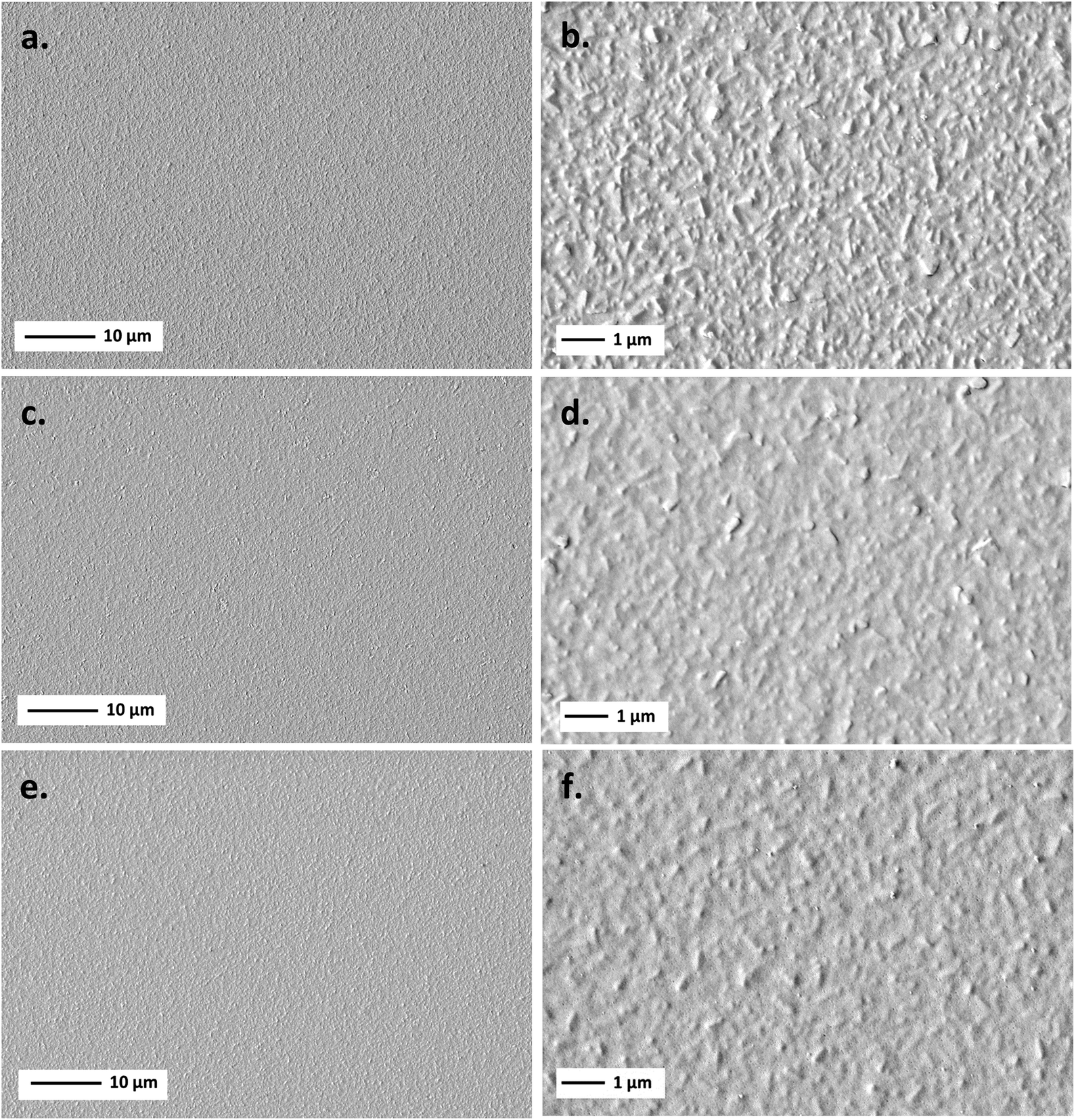 | ||
| Fig. 3 FE-SEM morphology at low and high magnification of BiTO 3 (a, b), BiTO 5 (c, d), and BiTO 7 (e, f) electrodes. | ||
As is clear from the low magnification micrographs, the whole set of electrodes is characterized by homogeneous BiTO coatings with no cracks or defects as a result of the tailored thermal annealing process developed (ESI, Table S2†). The substrate effect, deriving from the high roughness of FTO-coated glass (ESI, Section S3†), is prominent on the thinner film (i.e., low depositions number), with a visibly decreased roughness going from 3 to 5 and 7 deposition electrodes as a result of the higher amount of material deposited.
These results were corroborated by AFM analysis. Fig. 4 shows representative 5 μm × 5 μm AFM topography images collected for the different BiTO electrodes. The absence of discontinuous islands in all the AFM micrographs suggests the uniform covering of the substrate in the whole set of analyzed samples, as previously observed from SE-FEM images. As is shown, the higher the number of spin-coating cycles (from 3 to 7) the less the contrast of the AFM image reported (i.e., difference in the z-scale) as a consequence of the filling of the gaps on the surface of the rough FTO substrate produced by the progressive addition of new BiTO layers. This is also verified by the roughness properties of the electrodes, with all the main roughness parameters decreasing with the increasing number of spin-coating cycles (Table 1), thus confirming the previously reported FE-SEM investigation.
 | ||
| Fig. 4 Representative atomic force microscopy (AFM) images of the topography of the BiTO electrodes with the increasing number of spin coating depositions, 3 (a), 5 (b), and 7 (c) respectively. The scale bar is 1 micron for all the images. | ||
| Sample | R a (nm) | R q (nm) |
|---|---|---|
| BiTO 3 | 11.0 ± 0.5 | 14.3 ± 0.5 |
| BiTO 5 | 8.3 ± 0.5 | 10.6 ± 0.5 |
| BiTO 7 | 6.7 ± 0.5 | 8.7 ± 0.5 |
3.2 Optical characterization
The bandgaps (Eg) of the as-obtained homogeneous BiTO electrodes were determined via spectrophotometric analysis. Transmittance spectra were collected (Fig. 5a) and the bandgaps were calculated by extrapolating the intercept of the linear section of the Tauc plot (Fig. 5b) obtained by applying the following Tauc equation (1):| αhν = A(hν − Eg)n | (1) |
 | ||
| Fig. 5 Transmittance spectra of the 3 (BiTO 3), 5 (BiTO 5), and 7 (BiTO 7) spin-coated layers (a) and relative Tauc plot (b) used for the extrapolation of the bandgaps. | ||
The presence of interference fringes in the transmittance curves confirms the uniformity in thickness, surface homogeneity, and the compact nature of the produced BiTO layers.73–76 The extrapolated bandgap values for the BiTO electrodes were (3.56 ± 0.01) eV, (3.55 ± 0.01) eV, and (3.54 ± 0.01) eV for BITO 3, BiTO 5, and BiTO 7 respectively, which are in line with previously reported values for thin-film BiTO compact layers.60,72,77
3.3 Electrochemical and photoelectrochemical characterization of the BiTO photo-electrodes
LSV measurements in the dark and under illumination (1 sun, AM 1.5, 100 mW cm−2) were then collected under reduction conditions (−1.5–0.2 V vs. Ag/AgCl) in a 0.1 M KHCO3 aqueous solution saturated with CO2 for the whole set of BiTO electrodes to assess the photo-electro activity of the layers and establish the best performing system in terms of the current density produced. LSV curves in the dark and under illumination for the whole set of BiTO electrodes are shown in Fig. 6. When illuminated, all the electrodes achieved higher values of current, verifying their photo-electrode character, with current density values registered under illumination conditions at the final potential (i.e., −1.5 V vs. Ag/AgCl) of (−2.8 ± 0.1), (−3.5 ± 0.1), and (−4.1 ± 0.3) mA cm−2 for BiTO 3, BiTO 5, and BiTO 7 respectively. An almost linear increment of current density at −1.5 V vs. Ag/AgCl was thus recorded under illumination going from BiTO 3 to BiTO 7 (ESI, Fig. S4.1†), with the latter reaching the highest current density values (Fig. 6c), and a photo-current density at −1.5 V vs. Ag/AgCl of (−1.5 ± 0.4) mA cm−2 as a result of the higher amount of photo-active material of this electrode. As is shown, a reduction peak around −1.2 V vs. Ag/AgCl is present in the voltammogram of all the tested BiTO photo-electrodes, probably attributable to the reduction of water, which is more thermodynamically favored at a lower potential. | ||
| Fig. 6 LSV analyses in the dark and under illumination for BiTO 3 (a), BiTO 5 (b), and BiTO 7 (c) and LSV curve under illumination of the whole set of electrodes for comparison (d). All the curves were recorded in a CO2 saturated 0.1 M KHCO3 aqueous solution. | ||
A control experiment performed using BiTO 7 in the same electrolyte (i.e., KHCO3 0.1 M degassed with Ar) but in the absence of CO2 (ESI, Fig. S4.2†) showed in fact a similar profile, thus confirming this assumption. However, the lower current density values (i.e., more positive J) and an onset potential shifted towards more negative potential compared to the same electrode tested in CO2-saturated KHCO3 verify a higher photo-electrochemical activity of the electrode towards CO2 reduction.78–80 The hydrogen evolution assumption via the water splitting reaction at potentials lower than −1.2 V (vs. Ag/AgCl) was therefore confirmed by analyzing gas samples collected during 1 h chronoamperometric measurements performed on BiTO 7 under illumination (1 sun, AM 1.5, and 100 mW cm−2) in the electrolyte of interest (CO2 saturated KHCO3 0.1 M) (ESI, Fig. S5†).
The higher photo-activity of the BiTO 7 sample shown by the LSV curves was corroborated by EIS analysis performed under dark and illumination conditions at a negative potential (i.e., −1.2 V vs. Ag/AgCl) in a non-redox electrolyte (i.e., KCl 0.1 M) in order to investigate the influence of the number of depositions on the charge transfer properties of the BiTO photo-electrodes. Nyquist plots for the whole set of electrodes are reported in Fig. 7. All the experimental values could be well-fitted with the equivalent circuit reported in the inset and the derived parameters are listed in Table 2. In the circuit, RCT represents the charge transfer resistance at the electrode/electrolyte interface, CPE1 (i.e., constant phase element) in parallel to RCT constitutes the capacity to accumulate charges at the double layer, therefore standing for the non-faradic phenomena, and Rs accounts for any and all resistances associated with solution resistance, wires, clips, or other contacts in the system.81 More in detail, RCT values correspond to the diameter of the arch-shaped segments visible in Nyquist plots. As expected, RCT values associated with illuminated curves are lower compared to those of dark curves, thus confirming the photoactive nature of the electrode. More interestingly, RCT decreases both under dark and illumination conditions going from 3 to 7 layers corroborating LSV measurements and proving an increased charge transfer ability for the sample with the highest amount of loaded material. The near-linear increase of these properties demonstrates that up to 7 depositions (i.e., BiTO 7) the critical thickness of BiTO electrodes was not reached.
 | ||
| Fig. 7 Nyquist plots for the 3 (BiTO 3), 5 (BiTO 5), and 7 (BiTO 7) spin-coated electrodes under dark (a) and illumination conditions (b) at −1.2 V (vs. Ag/AgCl) in 0.1 M KCl aqueous solution. | ||
| Sample | R CT – dark (kΩ) | R CT – light (kΩ) |
|---|---|---|
| BiTO 3 | 3.89 ± 0.07 | 2.68 ± 0.03 |
| BiTO 5 | 2.47 ± 0.04 | 1.63 ± 0.03 |
| BiTO 7 | 1.88 ± 0.08 | 1.24 ± 0.02 |
In other words, this indicates that the number of electrons effectively available for reduction processes in the BiTO multi-layered electrodes up to 7 consecutive depositions does not decrease as a consequence of the increased electron diffusion path and charge recombination processes.
This was verified by means of Mott–Schottky (MS) analyses. The MS plot reporting the reciprocal squared values of the layer capacitance (1/C2) at 1 kHz vs. the applied potential (E) is shown in Fig. 8 for BiTO electrodes with different layers numbers. As indicated by the positive slope of the linear segment, the BTO layers behave like an n-type semiconductor for which the Mott–Schottky equation is (2):82
 | (2) |
 | (3) |
 | ||
| Fig. 8 Mott–Schottky plot of the BiTO layers with a different number of depositions (a) and energy diagram of the BiTO 7 photo-electrode vs. NHE (pH = 7) compared with the redox potential of CO2 conversion reactions (b). | ||
As is shown, the slope of the linear segments decreases with the increasing thickness of the BiTO layer as a result of the increased density of charges, as described by eqn (3). Assuming the interfacial area constant for all the layers and approximated to the geometric area of the tested electrodes, ND values of (6.4 × 1024) m−3, (1.5 × 1025) m−3, and (2.3 × 1025) m−3 for BiTO 3, BiTO 5, and BiTO 7 respectively were obtained, verifying the highest number of electrons in the BiTO 7 photoelectrode.
All these results (i.e., LSV, EIS, and MS measurements) indicate the BiTO 7 electrode as the best performing system among the ones tested and it is, therefore, the only one considered in the next part of this work. The flat band potential (Efb) of the optimized electrode was determined from the intercept (E = −0.971 V vs. Ag/AgCl, ESI Fig. S6†) of the MS curve on the potential axis as follows (4):
 | (4) |
The calculated BiTO Efb value vs. Ag/AgCl was converted to the Normal Hydrogen Electrode (NHE) scale according to the Nernst equation (5):
| ENHE = EAg/AgCl + 0.0591 pH + E0Ag/AgCl | (5) |
The charge transfer properties of BiTO 7 in the dark and under different illumination conditions (i.e., front and back illumination) in the electrolyte of interest (i.e. CO2 saturated KHCO3) were therefore studied at 0 V (vs. Ag/AgCl) and under reduction conditions at a potential of −0.8 V (vs. Ag/AgCl) (i.e., at a potential at which the water reduction reaction does not occur on the surface of the electrode) to define the most appropriate illumination conditions. Fig. 9 reports the Nyquist plot of the BiTO 7 sample. All the experimental data were fitted using the previously reported circuit model (Fig. 7) and the relative RCT values are listed in Table S8 (ESI).†
 | ||
| Fig. 9 Nyquist plot of the 130 nm thick BiTO electrode (BiTO 7) at 0 and −0.8 V (vs. Ag/AgCl) in the dark and under different illumination conditions (i.e., front and back illumination) in CO2-saturated 0.1 M KHCO3 aqueous solution. | ||
As previously observed, for both the applied potentials, the impedance spectra recorded under light are characterized by smaller arches compared to the corresponding dark curves, meaning that the charge transfer ability of the samples is enhanced as a result of the higher number of charges available generated from the photoexcitation process.
In addition, the charge transfer properties of the BiTO electrode are enhanced at negative potential because of the higher number of electrons available deriving from the applied external negative bias. The reason for that relies on the n-type semiconducting character of BiTO. When a negative potential is applied electrons start moving within the material towards the surface and can be therefore transferred to the electrolyte species. It is worth noting that the back illumination leads to smaller RCT for both the applied voltages. Excluding the slightly smaller amount of light reaching the sample as a result of the absorption of part of the radiation by the electrolyte when the frontal illumination is applied, the reason for that can be attributable to the location of photo-generated holes. When the sample is frontally illuminated, a higher density of holes is located on the surface of the electrodes where the irradiation is maximum. This of course hinders the transfer of electrons to the electrolyte due to the higher recombination probability. In contrast, when the light strikes the layers from the back of the sample, a higher concentration of holes and consequently a higher probability of charge recombination are located on the back of the BiTO layers so that the charge transfer properties at the electrode/electrolyte interface are not compromised.
To assess, understand and study the influence of BiTO ferroelectric properties on the photo-electrochemical performances, electrodes were then subjected to electric poling. LSV curves under back illumination at different poling states under reaction conditions (i.e., CO2 saturated 0.1 M KHCO3) are shown in Fig. 10 together with the time-dependent photo-current density of the sample under chopped light irradiation. As is shown (Fig. 10a), an increment of the produced photo-current is achieved when negative poling is applied, while the positively poled BiTO electrode displays a decreased photo-current. The time-dependent current density curves with ON/OFF illumination when no external bias is applied (Fig. 10b) show a value of current density almost double for negatively poled samples compared to positively poled films (J ∼ 1.1 μA cm−2vs. 0.6 μA cm−2). This difference is further increased at negative potentials, with a current density value five times higher for negative poling compared to the positively poled sample at −0.6 V (J ∼ 25 μA cm−2vs. 6 μA cm−2) and doubled compared to the unpoled sample (J of 13 μA cm−2) (Fig. 10c). This increment suggests a more efficient charge separation (i.e., lower charge recombination) in the negatively poled BiTO electrode as a result of the ferroelectric potential within the material. Moreover, the registered current density value at zero potential, when no poling is applied (i.e., J ∼ 0.65 μA cm−2), is higher than the ones reported for analogous pure BiTO layers of 0.18 μA cm−256 and 0.075 μA cm−2,57 for photovoltaic applications.
 | ||
| Fig. 10 LSV of the illuminated BiTO 7 sample under different poling states (a) and current–time dependent curve under chopped light irradiation in different poling states at 0 V (vs. Ag/AgCl) (b) and at −0.6 V (vs. Ag/AgCl) (c). Nyquist plot of the BiTO 7 electrode at −0.6 V (vs. Ag/AgCl) in backside illumination under negative poling compared to the unpoled sample in 0.1 M KHCO3 aqueous solution (d). | ||
To study the effect of the ferroelectric potential on the charge-transfer process of the BiTO layers, EIS measurements under reduction conditions (−0.6 V vs. Ag/AgCl, in CO2 saturated 0.1 M KHCO3) were carried out under illumination. The Nyquist plot under backside illumination of the BiTO photo-electrode under negative poling (i.e., optimal conditions) compared to the unpoled sample as a reference is reported in Fig. 10d. The experimental data were fitted using the previously reported circuit model (Fig. 6). As evident, the charge transfer resistance associated with the negatively poled electrode under reduction conditions (i.e., negative potential applied) is much smaller than that of the pristine sample (i.e., (8.9 ± 0.4) kΩ for the negatively poled sample vs. (1.4 ± 0.3) × 102 kΩ when no poling is applied), thus indicating a faster interfacial electron transfer from the BiTO poled electrode to the acceptor species of the electrolyte (i.e., HCO3− and CO32−).
The observed enhanced photoelectrochemical performance in terms of improved charge separation (i.e., enhanced current–density) and surface charge-transfer ability of negative polarized BiTO photocathodes can be explained in terms of change in the band bending at the electrode interface as a result of the ferroelectric polarization. Fig. 11a shows the proposed schematic band diagram for the BiTO photo-electrode electrically connected to the metal counter electrode (Pt wire) when no external potential is applied. In the system, a Schottky contact is established between the FTO and the deposited BiTO as a result of the highly conductive nature of the substrate84 and, on the other side, an upward band bending of the n-semiconductor at the BiTO-electrolyte interface takes place in order to equilibrate their electrochemical potential (i.e., Fermi level).85 This upward bending acts as a barrier to electron transfer so that when electrons are photogenerated they tend to drift towards the semiconductor bulk and holes are injected into the electrolyte. This explains the positive current value obtained at zero potential (Fig. 10b).
 | ||
| Fig. 11 Energy band diagrams for the BiTO photo-electrode in the considered photo-electrochemical cell with a Pt counter electrode and a CO2-saturated KHCO3 electrolyte with no bias (a) and when a negative bias (d) is applied to the cell, and effect of the ferroelectric potential on the BiTO band bending when a negative (b, e) and positive (c, d) poling are applied. The coloured bar represents the polarization electric field profile along the BiTO electrode thickness; red for positive and blue for negative. | ||
When a negative potential is induced by polarization on the surface of the BiTO electrode in contact with the electrolyte (Fig. 11b), an upwards bending is produced as a result of the developed ferroelectric potential.29 The driving force for the photo-generated electrons to reach the bulk of BiTO is thus enhanced and simultaneously the holes are more driven to be transferred to the electrolyte species.
On the other side of the electrode, an opposite effect is achieved, the Schottky barrier height is decreased, thus facilizing electron injection in the conductive FTO substrate. An overall more efficient charge separation takes place resulting in a higher photo-generated current (Fig. 10b). A reversed effect is in contrast obtained when the polarization through the electrode is inverted (i.e., positive poling) (Fig. 11c), thus explaining the reduced photocurrent registered (Fig. 10b). Electrons are less driven to be transferred to the FTO because of the higher Schottky barrier and the possibility of electron–hole recombination is therefore enhanced. On the other hand, different aspects need to be considered when a negative bias is applied to the BiTO photo-electrode to promote surface reduction reactions. The application of an external bias in the semiconductor is an effective way to control the Fermi level within the material, thus representing an efficient strategy to improve the charge separation within the semiconductor and facilitate the reaction of the desired charge carriers on its surface.86 The application of an external negative voltage induces in an n-type material a reduction of the electrolyte interface band bending (or even the elimination) such that the electrons transfer from the material to the electrolyte become favoured87 (Fig. 11d). The coupling of this external voltage and of the associated generated electric field with the depolarization electric field created with the remnant polarization needs therefore to be considered. When a positive polarization is applied to the BiTO photo-electrode, a depolarization field (Edp) is formed so that it points towards the FTO substrate in accordance with depolarization field theory. This depolarization field is opposite in direction to the applied electric field generated by the external voltage so that the overall produced effect is a reduction of the available energy to promote electron injection in the electrolyte (Fig. 11f). In other words, the resulting potential-induced band bending is reduced, thus consequently reducing the registered photo-current (Fig. 10a and c). From a different perspective, when positive poling is applied, the positive local charges induced on the surface of the BiTO photocathodes can recombine with the photo-generated electrons and with the electrons associated with the applied negative bias so that a reduced available number of electrons is effectively available for reduction processes. In contrast a negative poling treatment switches the resulting depolarization field towards the electrolyte so that the resulting electric field available to separate the photogenerated charges is enhanced by superimposing the two electric fields in the same direction56 (Fig. 11e).
An overall downward bending is thus obtained, which explains the higher photocurrent registered, a direct consequence of the reduced charge recombination, and the lower electron transfer resistance (Fig. 10d). This, therefore, demonstrates the possibility of effectively adopting a ferroelectric polarization (i.e., internal electric field) coupled with the application of an external bias (i.e., an external electric field) to control the migration of photo-generated charges in BiTO photo-electrodes for the photo-electrochemical reduction of carbon dioxide.
4 Conclusions
In this work, highly transparent, spin-coated Bi4Ti3O12 (BiTO) homogeneous and compact layers with a different number of depositions were successfully fabricated on FTO-coated glass substrates to be used as photocathodes for the ferroelectric-enhanced photoelectrochemical reduction of CO2. The as-obtained layers were fully characterized from a structural and morphological point of view. The influence of the number of spin-coating cycles on the optical characteristics and on the main photo-electrochemical properties was thus evaluated, and BiTO 7 (i.e., 7 depositions) was identified as the optimal BiTO photo-cathode based on the produced current density (i.e. −4.1 mA cm−2 at −1.5 V vs. Ag/AgCl), on the superior charge-transfer properties assessed by EIS measurement, and on the higher charge carrier density (ND of 2.3 × 1025 m−3). The effect of the ferroelectric polarization on the PEC performances of the produced BiTO photo-electrode was then investigated, and under negative polarization, a current density increment of about 50% (i.e., −30 μA cm−2 and −20 μA cm−2 at −0.6 V vs. Ag/AgCl for negatively and not poled samples respectively) and a reduced charge transfer resistance (i.e., RCT of about 9 kΩ and 140 kΩ for negatively and unpoled samples respectively) were registered, which could be explained based on the band bending at the photo-electrode/electrolyte interface caused by the superimposition of the generated ferroelectric potential with the applied external bias.This work, therefore, demonstrates the possibility of exploiting an externally induced ferroelectric potential on thin film BiTO photocathodes to modulate the PEC performances in ferroelectric-assisted CO2 photo-electrochemical reduction.
Author contributions
Formal analysis: S. C. and A. C; investigation: S. C. and A. C.; conceptualization: S. C., A. G., N. S., and A. S.; methodology: S. C., A. G., and N. S.; writing – original draft: S. C., A. G., and N. S.; writing – review & editing: S. C., A. G., N. S., and A. C.; visualization: S. C.; supervision: A. G. and A. S.; project administration: A. G. and A. S.; funding acquisition: A. S.Conflicts of interest
There are no conflicts to declare.Acknowledgements
This work was financially supported by the Research Program Progetti@CNR of the National Research Council of Italy, under the name of “RIPRESA” Project (integrated piezo-phototronic devices for carbon dioxide reduction to liquid solar fuels).Notes and references
- X. Chen, R. T. Guo, L. F. Hong, Y. Yuan and W. G. Pan, Energy Fuels, 2021, 35, 19920–19942 CrossRef CAS.
- M. Madi, M. Tahir and S. Tasleem, J. Environ. Chem. Eng., 2021, 9, 106264 CrossRef CAS.
- X. Liu, J. Xiao, S. Ma, C. Shi, L. Pan and J. J. Zou, ChemNanoMat, 2021, 7, 684–698 CrossRef CAS.
- L. Ye, Y. Deng, L. Wang, H. Xie and F. Su, ChemSusChem, 2019, 12, 3671–3701 CrossRef CAS PubMed.
- G. A. Kallawar, D. P. Barai and B. A. Bhanvase, J. Cleaner Prod., 2021, 318, 128563 CrossRef CAS.
- Z. Chen, H. Jiang, W. Jin and C. Shi, Appl. Catal., B, 2016, 180, 698–706 CrossRef CAS.
- W. Wei, Y. Dai and B. Huang, J. Phys. Chem. C, 2009, 113, 5658–5663 CrossRef CAS.
- S. Tu, Y. Zhang, A. H. Reshak, S. Auluck, L. Ye, X. Han, T. Ma and H. Huang, Nano Energy, 2019, 56, 840–850 CrossRef CAS.
- K. Das, D. Majhi, R. Bariki and B. G. Mishra, ChemistrySelect, 2020, 5, 1567–1577 CrossRef CAS.
- L. Wang, H. Li, S. Zhang, Y. Long, L. Li, Z. Zheng, S. Wu, L. Zhou, Y. Hei, L. Luo and F. Jiang, Solid State Sci., 2020, 100, 106098 CrossRef CAS.
- Z. Liu and Z. Ma, RSC Adv., 2020, 10, 19232–19239 RSC.
- G. Shen, Y. Pu, R. Sun, Y. Shi, Y. Cui and P. Jing, New J. Chem., 2019, 43, 12932–12940 RSC.
- M. Shen, Y. Shi, Z. Wang, T. Wu, L. Hu and L. Wu, J. Colloid Interface Sci., 2022, 608, 2529–2538 CrossRef CAS PubMed.
- H. Sun, Z. Xu, X. Xie, J. Niu, M. Wang, X. Zhang, X. Chen and J. Han, J. Alloys Compd., 2021, 882, 160609 CrossRef CAS.
- C. Liu, J. Xu, J. Niu, M. Chen and Y. Zhou, Sep. Purif. Technol., 2020, 241, 116622 CrossRef CAS.
- M. J. Chang, W. N. Cui, J. Liu, K. Wang, H. L. Du, L. Qiu, S. M. Fan and Z. M. Luo, J. Mater. Sci. Technol., 2020, 36, 97–105 CrossRef CAS.
- H. Shi, J. Fu, W. Jiang, Y. Wang, B. Liu, J. Liu, H. Ji, W. Wang and Z. Chen, Colloids Surf., A, 2021, 615, 126063 CrossRef CAS.
- A. Kumar, G. Sharma, A. Kumari, C. Guo, M. Naushad, D. V. N. Vo, J. Iqbal and F. J. Stadler, Appl. Catal., B, 2021, 284, 119808 CrossRef CAS.
- H. Gao, X. Zhao, H. Zhang, J. Chen, S. Wang and H. Yang, J. Electron. Mater., 2020, 49, 5248–5259 CrossRef CAS.
- L. Liu, H. Huang, F. Chen, H. Yu, N. Tian, Y. Zhang and T. Zhang, Sci. Bull., 2020, 65, 934–943 CrossRef CAS.
- X. Wang, Y. Wang, M. Gao, J. Shen, X. Pu, Z. Zhang, H. Lin and X. Wang, Appl. Catal., B, 2020, 270, 118876 CrossRef CAS.
- Y. Wang, X. Zhang, C. Zhang, R. Li, Y. Wang and C. Fan, Inorg. Chem. Commun., 2020, 116, 107931 CrossRef CAS.
- C. Zhang, Y. Wang, X. Zhang, R. Wang, L. Kou, J. Wang, R. Li and C. Fan, Chem. Eng. J., 2021, 417, 128218 CrossRef CAS.
- N. Li, Y. Kong, Q. Shen, K. Wang, N. Wang and J. Zhou, J. Photonics Energy, 2021, 11, 026501 CAS.
- Q. Zhou, B. J. Kennedy and C. J. Howard, Chem. Mater., 2003, 15, 5025–5028 CrossRef CAS.
- Q. Zhang, Y. Shi, X. Shi, T. Huang, S. Lee, Y. Huang and J. ji Cao, Appl. Catal., B, 2022, 302, 120876 CrossRef CAS.
- S. Tu, H. Huang, T. Zhang and Y. Zhang, Appl. Catal., B, 2017, 219, 550–562 CrossRef CAS.
- S. Tu, Y. Guo, Y. Zhang, C. Hu, T. Zhang, T. Ma and H. Huang, Adv. Funct. Mater., 2020, 30, 2005158 CrossRef CAS.
- L. Pan, S. Sun, Y. Chen, P. Wang, J. Wang, X. Zhang, J. J. Zou and Z. L. Wang, Adv. Energy Mater., 2020, 10, 2000214 CrossRef CAS.
- L. Liu, H. Huang, Z. Chen, H. Yu, K. Wang, J. Huang, H. Yu and Y. Zhang, Angew. Chem., Int. Ed., 2021, 60, 18303–18308 CrossRef CAS PubMed.
- Y. Tian, A. Wang, Y. Wei, M. Pei, R. Cao, Z. Gu, Q. Yuan, Y. Hu, J. Wang, K. Liu, D. Shang, J. Niu, X. An, R. Long and J. Zhang, Adv. Funct. Mater., 2022, 2111180 CrossRef CAS.
- Y. L. Huang, W. S. Chang, C. van Nguyen, H. J. Liu, K. A. Tsai, J. W. Chen, H. H. Kuo, W. Y. Tzeng, Y. C. Chen, C. L. Wu, C. W. Luo, Y. J. Hsu and Y. H. Chu, Nanoscale, 2016, 8, 15795–15801 RSC.
- D. Cao, Z. Wang, L. Wen, Y. Mi, Y. Lei, D. Cao, Z. Wang, L. Wen, Y. Mi and Y. Lei, Angew. Chem., 2014, 126, 11207–11211 CrossRef.
- Y. Ren, F. Nan, L. You, Y. Zhou, Y. Wang, J. Wang, X. Su, M. Shen and L. Fang, Small, 2017, 13, 1603457 CrossRef PubMed.
- Y. Wang, M. Zhang, Y. Yue, H. Zhang, A. Mahajan, S. Dunn and H. Yan, Sol. RRL, 2022, 6, 2200124 CrossRef CAS.
- S. Wang, F. Nan, Y. Zhou, F. Zheng, Y. Weng, L. You and L. Fang, J. Appl. Phys., 2020, 128, 154101 CrossRef CAS.
- J. Huang, Y. Wang, X. Liu, Y. Li, X. Hu, B. He, Z. Shu, Z. Li and Y. Zhao, Nano Energy, 2019, 59, 33–40 CrossRef CAS.
- Q. Liu, Y. Zhou, L. You, J. Wang, M. Shen and L. Fang, Appl. Phys. Lett., 2016, 108, 022902 CrossRef.
- X. Wu, H. Li, X. Wang, L. Jiang, J. Xi, G. Du and Z. Ji, J. Alloys Compd., 2019, 783, 643–651 CrossRef CAS.
- A. Radmilovic, T. J. Smart, Y. Ping and K.-S. Choi, Chem. Mater., 2020, 32, 3262–3270 CrossRef CAS.
- W. Wang, Y. Weng, B. Tu, Y. Zhou, F. Zheng, L. Fang and L. You, AIP Adv., 2021, 11, 095110 CrossRef CAS.
- Z. Liu, L. Wang, X. Yu, J. Zhang, R. Yang, X. Zhang, Y. Ji, M. Wu, L. Deng, L. Li and Z. L. Wang, Adv. Funct. Mater., 2019, 29, 1807279 CrossRef CAS.
- Y. Cui, H. Sun, J. Briscoe, R. Wilson, N. Tarakina, S. Dunn and Y. Pu, Nanotechnology, 2019, 30, 255702 CrossRef CAS PubMed.
- A. Augurio, A. Alvarez-Fernandez, V. Panchal, B. Pittenger, P. De Wolf, S. Guldin and J. Briscoe, ACS Appl. Mater. Interfaces, 2022, 14, 13147–13157 CrossRef CAS PubMed.
- L. Yang, Y. Xiong, W. Guo, M. Zhou, K. Song, P. Xiao and G. Cao, Nano Energy, 2018, 44, 63–72 CrossRef CAS.
- S. Li, J. Zhang, B. P. Zhang, W. Huang, C. Harnagea, R. Nechache, L. Zhu, S. Zhang, Y. H. Lin, L. Ni, Y. H. Sang, H. Liu and F. Rosei, Nano Energy, 2017, 35, 92–100 CrossRef CAS.
- S. Singh and N. Khare, Nano Energy, 2017, 42, 173–180 CrossRef CAS.
- D. Yu, Z. Liu, J. Zhang, S. Li, Z. Zhao, L. Zhu, W. Liu, Y. Lin, H. Liu and Z. Zhang, Nano Energy, 2019, 58, 695–705 CrossRef CAS.
- S. Singh and N. Khare, Appl. Phys. Lett., 2017, 110, 152902 CrossRef.
- C. Tan, J. Wang, X. Zhong, J. Jiang, X. Zhang and Y. Ding, Mater. Des., 2017, 129, 186–191 CrossRef CAS.
- Y. He, P. Shen, Y. Liu, M. Chen, D. Cao and X. Yan, Mater. Sci. Semicond. Process., 2021, 121, 105351 CrossRef CAS.
- S. Wang, F. Zheng, Y. Weng, G. Yuan, L. Fang and L. You, Adv. Mater. Interfaces, 2020, 7, 2000185 CrossRef CAS.
- X. He, B. Lin, L. Yang, C. Shang, S. Li, Z. Chen and X. Wang, Energy Fuels, 2020, 34, 16927–16935 CrossRef CAS.
- S. Singh, A. L. Sangle, T. Wu, N. Khare and J. L. MacManus-Driscoll, ACS Appl. Mater. Interfaces, 2019, 11, 45683–45691 CrossRef CAS PubMed.
- F. Wu, Y. Yu, H. Yang, L. N. German, Z. Li, J. Chen, W. Yang, L. Huang, W. Shi, L. Wang and X. Wang, Adv. Mater., 2017, 29, 1701432 CrossRef PubMed.
- H. He, Z. He, Z. Jiang, J. Wang, T. Liu and N. Wang, J. Alloys Compd., 2017, 694, 998–1003 CrossRef CAS.
- Y. G. Zhang, H. W. Zheng, J. X. Zhang, G. L. Yuan, W. X. Gao, Y. Z. Gu, C. L. Diao, Y. F. Liu and W. F. Zhang, Mater. Lett., 2014, 125, 25–27 CrossRef CAS.
- Q. Zhao, Q. Zhang, J. Ren, Z. He and H. He, J. Mater. Sci.: Mater. Electron., 2020, 31, 7060–7066 CrossRef CAS.
- A. Al-Keisy, L. Ren, X. Xu, W. Hao, S. X. Dou and Y. Du, J. Phys. Chem. C, 2019, 123, 517–525 CrossRef CAS.
- S. Ranjbar, A. Ranjbar, M. Behdani and M. Rezaei Roknabadi, Sci. Iran., 2019, 26, 1990–1996 Search PubMed.
- W. L. Zhang, M. H. Tang, Y. Xiong, K. Wang, Z. P. Wang, Y. G. Xiao, S. A. Yan, Z. Li and J. He, RSC Adv., 2016, 6, 88668–88673 RSC.
- S. Sruthi, A. Adarsh, A. Veronica, M. Saideep and S. Dutta, J. Mater. Sci.: Mater. Electron., 2016, 27, 4062–4067 CrossRef CAS.
- W. F. Su and Y. T. Lu, Mater. Chem. Phys., 2003, 80, 632–637 CrossRef CAS.
- Y. M. Kan, P. L. Wang, Y. X. Li, Y. B. Cheng and D. S. Yan, Key Eng. Mater., 2002, 224–226, 597–600 CAS.
- J. Lelievre and P. Marchet, J. Alloys Compd., 2018, 732, 178–186 CrossRef CAS.
- D. Valerini, S. Hernández, F. di Benedetto, N. Russo, G. Saracco and A. Rizzo, Mater. Sci. Semicond. Process., 2016, 42, 150–154 CrossRef CAS.
- D. Hidalgo, R. Messina, A. Sacco, D. Manfredi, S. Vankova, E. Garrone, G. Saracco and S. Hernández, Int. J. Hydrogen Energy, 2014, 39, 21512–21522 CrossRef CAS.
- G. Saracco, G. Barbero, S. Hernández and A. L. Alexe-Ionescu, J. Electroanal. Chem., 2017, 788, 61–65 CrossRef CAS.
- N. Sangiorgi, L. Aversa, R. Tatti, R. Verucchi and A. Sanson, Opt. Mater., 2017, 64, 18–25 CrossRef CAS.
- J. Liu, M. Sun, M. J. Chang, W. N. Cui, C. M. Zhang, F. R. Ni, J. Zhang, S. M. Fan and H. L. Du, J. Phys. Chem. Solids, 2021, 157, 110179 CrossRef CAS.
- S. Lardhi, D. Noureldine, M. Harb, A. Ziani, L. Cavallo and K. Takanabe, J. Chem. Phys., 2016, 144, 134702 CrossRef PubMed.
- C. Jia, Y. Chen and W. F. Zhang, J. Appl. Phys., 2009, 105, 113108 CrossRef.
- N. Guermat, W. Daranfed, I. Bouchama and N. Bouarissa, J. Mol. Struct., 2021, 1225, 129134 CrossRef CAS.
- A. Sangiorgi, R. Bendoni, N. Sangiorgi, A. Sanson and B. Ballarin, Ceram. Int., 2014, 40, 10727–10735 CrossRef CAS.
- N. Houaidji, M. Ajili, B. Chouial, N. T. Kamoun, K. Kamli, A. Khadraoui, Z. Hadef, B. Zaidi and B. Hadjoudja, J. Nano Res., 2020, 65, 13–26 CAS.
- B. Khalfallah, I. Riahi and F. Chaabouni, Opt. Quantum Electron., 2021, 53, 1–14 CrossRef.
- P. Wollmann, B. Schumm and S. Kaskel, Solid State Sci., 2012, 14, 1378–1384 CrossRef CAS.
- H. Y. Jeong, M. Balamurugan, V. S. K. Choutipalli, E. S. Jeong, V. Subramanian, U. Sim and K. T. Nam, J. Mater. Chem. A, 2019, 7, 10651–10661 RSC.
- B. Ávila-Bolívar, L. García-Cruz, V. Montiel and J. Solla-Gullón, Molecules, 2019, 24, 2032 CrossRef PubMed.
- Z. Han, R. Kortlever, H. Y. Chen, J. C. Peters and T. Agapie, ACS Cent. Sci., 2017, 3, 853–859 CrossRef CAS PubMed.
- A. R. C. Bredar, A. L. Chown, A. R. Burton and B. H. Farnum, ACS Appl. Energy Mater., 2020, 3, 66–98 CrossRef CAS.
- A. Hankin, F. E. Bedoya-Lora, J. C. Alexander, A. Regoutz and G. H. Kelsall, J. Mater. Chem. A, 2019, 7, 26162–26176 RSC.
- P. C. Joshi, A. Mansingh, M. N. Kamalasanan and S. Chandra, Appl. Phys. Lett., 1991, 59, 2389–2390 CrossRef CAS.
- W.-J. Lang and Z.-Q. Li, Appl. Phys. Lett., 2014, 105, 042110 CrossRef.
- K. Rajeshwar, Encycl. Electrochem., 2007, 1–53 Search PubMed.
- G. G. Bessegato, T. T. Guaraldo, J. F. de Brito, M. F. Brugnera and M. V. B. Zanoni, Electrocatalysis, 2015, 6, 415–441 CrossRef CAS.
- C. Jiang, S. J. A. Moniz, A. Wang, T. Zhang and J. Tang, Chem. Soc. Rev., 2017, 46, 4645–4660 RSC.
Footnote |
| † Electronic supplementary information (ESI) available: XRD analysis at different temperatures, thermal analysis, characterization of the FTO substrate (SEM and AFM), additional LSV investigation, hydrogen evolution, Mott–Schottky analysis, and fitting data of EIS analysis. See DOI: https://doi.org/10.1039/d2se01372j |
| This journal is © The Royal Society of Chemistry 2023 |