
 Open Access Article
 This Open Access Article is licensed under a Creative Commons Attribution-Non Commercial 3.0 Unported Licence
Molecular engineering of nitrogen-rich helicene based organic semiconductors for stable perovskite solar cells†
Yuefang
Wei
,
Yaohang
Cai
,
Lifei
He
,
Yuyan
Zhang
,
Yi
Yuan
*,
Jing
Zhang
and
Peng
Wang
 *
*
State Key Laboratory of Silicon and Advanced Semiconductor Materials, Department of Chemistry, Zhejiang University, Hangzhou 310030, China. E-mail: yyuan@zju.edu.cn; pw2015@zju.edu.cn
First published on 7th September 2023
Abstract
Polycyclic heteroaromatics play a pivotal role in advancing the field of high-performance organic semiconductors. In this study, we report the synthesis of a pyrrole-bridged double azahelicene through intramolecular oxidative cyclization. By incorporating bis(4-methoxyphenyl)amine (OMeDPA) and ethylenedioxythiophene-phenyl-OMeDPA (EP-OMeDPA) into the sp3-nitrogen rich double helicene framework, we have successfully constructed two organic semiconductors with ionization potentials suitable for application in perovskite solar cells. The amorphous films of both organic semiconductors exhibit hole density-dependent mobility and conductivity. Notably, the organic semiconductor utilizing EP-OMeDPA as the electron donor demonstrates superior hole mobility at a given hole density, which is attributed to reduced reorganization energy and increased centroid distance. Moreover, this organic semiconductor exhibits a remarkably elevated glass transition temperature of up to 230 °C and lower diffusivity for external small molecules and ions. When employed as the p-doped hole transport layer in perovskite solar cells, TMDAP-EP-OMeDPA achieves an improved average efficiency of 21.7%. Importantly, the solar cell with TMDAP-EP-OMeDPA also demonstrates enhanced long-term operational stability and storage stability at 85 °C. These findings provide valuable insights into the development of high-performance organic semiconductors, contributing to the practical application of perovskite solar cells.
1. Introduction
Organic semiconductors are crystalline or amorphous materials comprised of molecules that aggregate through van der Waals forces.1–5 These molecules typically consist of carbon and hydrogen atoms, as well as heteroatoms such as oxygen, sulfur, and nitrogen, and possess conjugated structures. In their intrinsic state, organic semiconductors with wide or intermediate bandgaps act as electrical insulators and can only be transformed into semiconductors through charge injection, photoexcitation, or doping.6 In the display industry, the incorporation of a doped organic charge transport layer is essential to meet technological maturity requirements.7 Furthermore, perovskite solar cells, which have repeatedly broken efficiency records, often employ a doped hole transport layer composed of spiro-OMeTAD (Fig. 1).8–10 Among the various organic semiconductors reported, spiro-OMeTAD exhibits a high energy level of the highest occupied molecular orbital (HOMO), facilitating efficient hole extraction, and is influenced by its nitrogen and oxygen atom content and specific atomic connectivity.11,12 This hole transport layer is deposited using solution processing and offers advantageous characteristics, including suitable hole conduction and a smooth morphology on the surface of the perovskite polycrystalline film. Despite its exceptional performance, this hole transport layer is susceptible to fracturing with increasing temperatures, resulting in a decline in device performance.13,14 Consequently, the development of the next generation of high-performance hole transport layers is of utmost importance.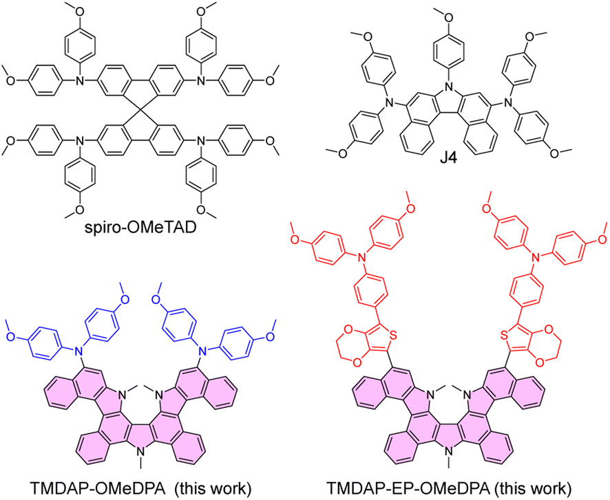 | ||
| Fig. 1 Molecular structures of organic semiconductors. The pyrrole-bridged double helicene was painted in magenta. | ||
The utilization of polycyclic aromatic hydrocarbons holds significant importance in the construction of high-mobility organic semiconductors. This is attributed to the ability of aromatic fusion to enhance the rigidity of π-conjugated systems and the carbon-to-hydrogen (C/H) ratio, thereby amplifying intermolecular charge transfer integrals and reducing the reorganization energy associated with charge transfer.15,16 Consequently, intermolecular charge hopping becomes more favorable. Notably, polycyclic aromatic hydrocarbon based organic semiconductors, such as pentacene and rubrene, exhibit exceptional charge mobility, surpassing 20 cm2 V−1 s−1.1 However, typical polycyclic aromatic hydrocarbons often possess a high degree of planarity, resulting in strong intermolecular noncovalent interactions and aggregation, which pose challenges in achieving solution-processed films with the desired thickness and uniformity required for practical optoelectronic devices. Hence, the introduction of multiple bulky and flexible side chains is often necessary to mitigate intermolecular self-aggregation and enable the application of polycyclic aromatic hydrocarbons in solution-processable thin-film optoelectronic devices. In recent years, extensive research has been conducted on large, two-dimensional extended polycyclic heteroaromatics incorporating nitrogen, oxygen, sulfur, boron, phosphorus, and other elements.17,18 By manipulating the topological structure of the π-conjugated system, including the fusion mode of aromatic rings and the number and composition of heteroatoms, various electronic structure-related properties can be tuned, including the bandgap, electronic absorption spectra, photoemission, and redox behavior. These distinctive characteristics make polycyclic heteroaromatics suitable as both p-type and n-type semiconductors in diverse organic optoelectronic devices. The presence of heteroatoms in polycyclic heteroaromatics facilitates the introduction of inherent dipole moments and provides opportunities for edge derivatization, offering additional means to control molecular solubility and self-assembly behavior.
Helicenes are a class of non-planar polycyclic aromatic hydrocarbons or polycyclic heteroaromatics with screw-shaped skeletons formed by the ortho-fusion of benzene or other aromatic rings.19–22 The presence of steric hindrance among the terminal aromatic rings endows helicenes with a helical structure and imparts helical chirality. In contrast to their planar counterparts, helicenes exhibit heightened solubility. As early as 1903, Meisenheimer and Wittes reported two variants of helicenes, specifically aza[5]helicene and benzo[f]naphtho[2,1-c]cinnoline.23 Subsequently, in 1927, Fuchs and Niszel synthesized aza[6]helicene.24 However, it was not until the year 1955 when Newman and colleagues accomplished the synthesis and resolution of hexahelicene, thereby igniting a surge of interest in helicene chemistry.25 Surprisingly, the development of the first-ever helicene-based semiconductor device did not materialize until 2009.26 Since then, an escalating number of helicene-based organic semiconductors have found application in organic light-emitting diodes, photodetectors, organic field-effect transistors, organic solar cells, and perovskite solar cells.27–33
Recently, prototypical helicenes, including oxa[5]helicene, thia[5]helicene, and aza[5]helicene, have been used as π-linkers in donor–π–donor type organic semiconductors for perovskite solar cells, achieving impressive efficiencies of up to 21.1% when combined with bis(4-methoxyphenyl)amine as the electron donor.34–36 Vailassery and Sun made a detailed review on the properties and device performance of helicene-based organic semiconductors for perovskite solar cells.37 Density functional theory calculations reveal that J4 (Fig. 1), featuring aza[5]helicene as the π-linker, exhibits a theoretical HOMO energy level of −4.79 eV, comparable to spiro-OMeTAD (−4.74 eV), while counterparts with oxa[5]helicene and thia[5]helicene display deeper HOMOs (−4.91 eV and −4.90 eV, respectively). However, organic semiconductors with deep HOMOs face challenges in achieving high hole density through air oxidation doping, resulting in limited direct-current conductivity. Additionally, the doped composite materials of these simple helicene-based organic semiconductors exhibit low glass transition temperatures below 70 °C, as determined by differential scanning calorimetry, imposing constraints on their application in the fabrication of thermally stable devices.
In this study, we synthesized a pyrrole-bridged double helicene, designated as DAP (highlighted in magenta in Fig. 1). By functionalizing the trimethylated DAP, referred to as TMDAP, with two bis(4-methoxyphenyl)amine electron donors, we successfully obtained TMDAP-OMeDPA (Fig. 1). Molecular dynamics simulations revealed that TMDAP-OMeDPA exhibited a theoretical glass transition temperature of 237 °C, significantly higher than that of J4 (167 °C). Furthermore, we introduced the 3,4-ethylenedioxythiophene-phenyl fragment between TMDAP and bis(4-methoxyphenyl)amine, leading to the construction of TMDAP-EP-OMeDPA (Fig. 1). Theoretical calculations demonstrated that TMDAP-EP-OMeDPA exhibited lower recombination energy and larger intermolecular centroid distance compared to TMDAP-OMeDPA, resulting in enhanced hole mobility. Moreover, molecular dynamics simulations indicated an even higher theoretical glass transition temperature of 276 °C for TMDAP-EP-OMeDPA. By utilizing doped TMDAP-EP-OMeDPA as a hole transport layer, we successfully fabricated perovskite solar cells with an average efficiency of 21.7%. The TMDAP-EP-OMeDPA cells also exhibited good operational stability and thermostability at 85 °C.
2. Results and discussion
2.1. Synthesis
The synthetic routes for TMDAP-OMeDPA and TMDAP-EP-OMeDPA are presented in Scheme 1. Initially, a solution of 7-methyl-7H-dibenzo[c,g]carbazole (1) in tetrahydrofuran underwent dropwise addition of 1.33 equivalents of N-bromosuccinimide in tetrahydrofuran at −20 °C, yielding 5-bromo-7-methyl-7H-dibenzo[c,g]carbazole (2) with a yield of 65%. By precisely controlling the reaction temperature, quantity of the nitration reagent, and addition method, 7-methyl-5-nitro-7H-dibenzo[c,g]carbazole (3) was obtained with a yield close to quantitative. Subsequently, compound 3 was reduced using hydrazinium hydrate and a palladium/activated carbon catalyst, resulting in 7-methyl-7H-dibenzo[c,g]carbazol-5-amine (4) with a yield of 92%. The Buchwald–Hartwig cross-coupling of compound 2 with compound 4 afforded bis(7-methyl-7H-dibenzo[c,g]carbazol-5-yl)amine (5) with an 87% yield. In the presence of the oxidant (2,6-dichloro-3,5-dicyano-1,4-benzoquinone), compound 5 underwent intramolecular oxidative cyclization, resulting in the formation of DMDAP with an 80% yield. The spatial structure of DMDAP was confirmed through single-crystal analysis, and the crystallographic data are provided in Table S1 of ESI.† Subsequently, DMDAP was methylated using iodomethane to quantitatively produce TMDAP. Further, at 0 °C, TMDAP reacted with two equivalents of NBS, leading to TMDAPBr2 with a yield of 96%. Finally, TMDAPBr2 underwent two-fold Buchwald–Hartwig cross-coupling with bis(4-methoxyphenyl)amine, yielding TMDAP-OMeDPA with an 85% yield. Additionally, the reaction of TMDAPBr2 with 4-(2,3-dihydrothieno[3,4-b][1,4]dioxin-5-yl)-N,N-bis(4-methoxyphenyl)aniline via a two-fold Pd-catalyzed direct arylation afforded TMDAP-EP-OMeDPA with an 86% yield. For detailed synthesis procedures and structural characterizations, including 1H NMR spectra, 13C NMR spectra, high-resolution mass spectra, and attenuated total reflectance Fourier-transform infrared spectra, please refer to ESI.† Notably, both organic semiconductors exhibited solubilities in chlorobenzene exceeding 160 mg mL−1.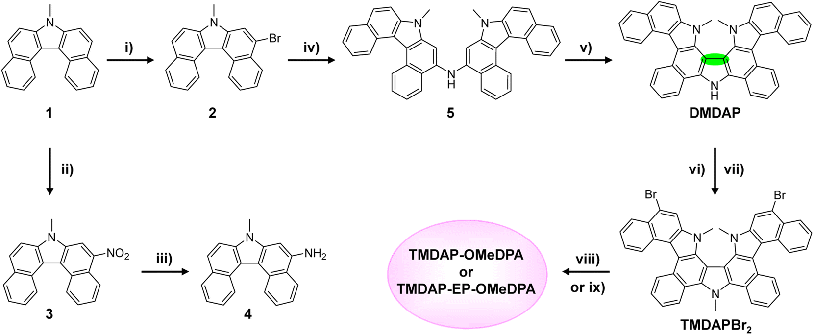 | ||
| Scheme 1 Synthetic routes. Reagents and conditions: (i) N-bromosuccinimide (1.33 equivalent), tetrahydrofuran, −20 °C, 0.5 h, 45%; (ii) nitric acid, trichloromethane, rt, 2 h, 98%; (iii) palladium/activated carbon, hydrazinium hydrate, tetrahydrofuran, rt, 0.5 h, 92%; (iv) 5-bromo-7-methyl-7H-dibenzo[c,g]carbazole, tris(dibenzylideneacetone)dipalladium, tri-tert-butylphosphine tetrafluoroborate, sodium tert-butoxide, toluene, 120 °C, 12 h, 87%; (v) (2,6-dichloro-3,5-dicyano-1,4-benzoquinone), toluene, rt, 0.5 h, 80%; (vi) sodium hydride, iodomethane, N,N-dimethylformamide, rt, 3 h, 98%; (vii) N-bromosuccinimide (2 equivalent), tetrahydrofuran, 0 °C, 1 h, 96%; (viii) bis(4-methoxyphenyl)amine, tris(dibenzylideneacetone)dipalladium, tri-tert-butylphosphine tetrafluoroborate, sodium tert-butoxide, toluene, 120 °C, 14 h, 85%; (ix) 4-(2,3-dihydrothieno[3,4-b][1,4]dioxin-5-yl)-N,N-bis(4-methoxyphenyl)aniline, palladium(II) acetate, tri(o-tolyl)phosphine, pivalic acid, potassium carbonate, N,N-dimethylformamide, 130 °C, 24 h, 86%. | ||
2.2. Energy level and hole extraction
The cyclic voltammograms and square wave voltammograms in a tetrahydrofuran solution are presented in Fig. 2A and B, respectively. Within the potential range of −0.2 V to 0.4 V, TMDAP-OMeDPA exhibits three overlapping oxidation-reduction waves in the cyclic voltammogram. However, their formal potentials can be precisely determined as 0.120 V, 0.198 V, and 0.320 V (relative to ferrocene) using square wave voltammetry. Within the same potential range, TMDAP-EP-OMeDPA shows two distinct oxidation–reduction waves. Based on peak current and half-wave width analysis, the first pair of oxidation-reduction waves corresponds to a two-electron process with an anodic peak potential of 0.165 V and a cathodic peak potential of 0.092 V. The second pair of oxidation-reduction waves has an anodic peak potential of 0.350 V and a cathodic peak potential of 0.287 V. By extracting the onset potential (Eonset) of the first oxidation wave from the cyclic voltammogram, we estimated the HOMO energy level (ECVH) of organic semiconductors using the formula ECVH = −5.10 − Eonset.38 The derived ECVH values for TMDAP-OMeDPA and TMDAP-EP-OMeDPA are −5.11 eV and −5.14 eV, respectively (Fig. 2A), indicating that extending π-conjugation does not necessarily result in a higher HOMO energy level. Under the same experimental conditions, spiro-OMeTAD and J4 exhibit ECVH values of −5.10 eV and −5.12 eV, respectively (Fig. S2†). Concurrently, the frontier orbital energy levels of these four molecular semiconductors were computed using the density functional theory method, as illustrated in Fig. 2C. Fig. 2D demonstrates a good linear correlation between the electrochemically measured HOMO energy levels and those calculated by density functional theory. We note that the theoretical HOMO values depend on the selection of functionals and basis sets, which normally cannot match the experimentally measured values exactly.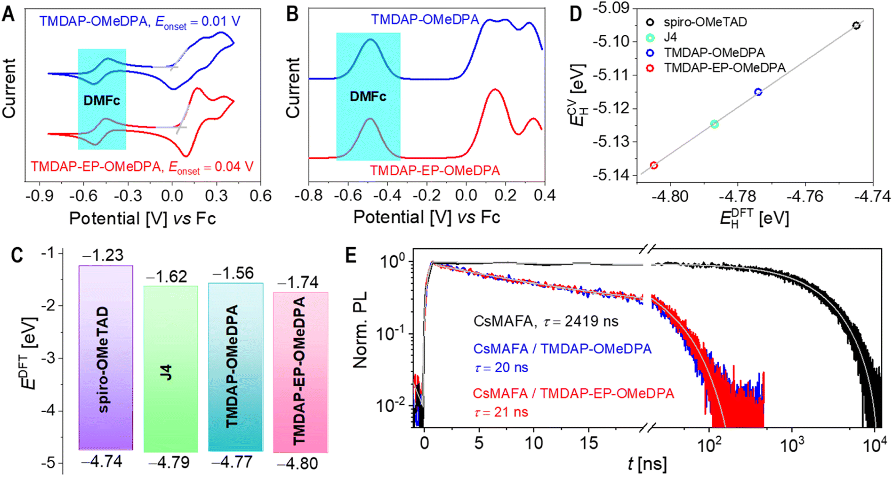 | ||
| Fig. 2 (A) Cyclic voltammograms with bis(pentamethylcyclopentadienyl)iron (DMFc) as the internal reference. The derived onset potential (Eonset) of the first oxidation wave is also presented. (B) Square wave voltammograms. (C) The lowest unoccupied molecular orbital energy levels (values above color bars) and the HOMO energy levels (EDFTH) (value under color bars) calculated by the density functional theory method at the B3LYP/6-311G(d,p) level. (D) Correlation between the HOMO energy levels from voltammetric measurement and theoretical calculation. (E) Time-resolved photoluminescence traces of CsMAFA perovskite films with and without an organic semiconductor layer. Note that the broken x-axis was set to be in a partially linear and partially logarithmic mode. The gray lines represent the biexponential fits of normalized photoluminescence intensity as a function of time (t), yielding the amplitude-averaged lifetime (τ). The excitation wavelength is 670 nm. | ||
Saliba et al. initially reported triple-cation lead halide perovskite alloys with excellent photostability.39 Following their work, we prepared a perovskite thin film with the chemical formula (CsPbI3)0.05(MAPbBr3)0.075(FAPbI3)0.875, denoted as CsMAFA, where MA represents the methylammonium cation and FA represents the formamidinium cation. Fig. 2E shows that the amplitude-averaged lifetime (τ) of the photoexcited state for CsMAFA on glass is 2.4 μs. Upon depositing a layer of spiro-OMeTAD, J4, TMDAP-OMeDPA, or TMDAP-EP-OMeDPA on the surface of the CsMAFA film, the τ value decreases to 19–21 ns (Fig. 2E and S3†), indicating that all four organic semiconductors can efficiently extract holes from the photoexcited perovskite with nearly 100% yield. The calculation details on photoluminescence lifetime and hole extraction yield can be found in Table S2.† The slight differences in hole extraction rates can be attributed to variations in the HOMO energy levels of the organic semiconductors, with higher HOMO energy levels leading to faster hole extraction. We remark that the design of organic semiconductors with proper HOMO energy levels is necessary for the quantitative carrier photogeneration for perovskite solar cells with the titania and tin oxide electron transport layers, which extract electrons with time constants of a few hundred nanoseconds.
2.3. Hole density, mobility, and conductivity
The efficiency of perovskite solar cell is intricately linked to the series resistance, including the resistance of hole transport layer. In addition to its thickness, the conductivity of the hole transport layer influences its resistance. To mitigate potential interference from interface charge transfer resistance, we employed a 10 μm-wide gold interdigital electrode to evaluate the conductivities (σ) of the nominally “pure” organic semiconductor thin films. When the channel widths were 5, 10, and 20 microns, there was no difference in the measured σ values, indicating that the effect of contact resistance could be ignored. The σ value of TMDAP-OMeDPA was measured as 0.06 μS cm−1, whereas that of TMDAP-EP-OMeDPA was found to be 0.42 μS cm−1, which is seven times higher than the former. Under equivalent test conditions, the σ values of spiro-OMeTAD and J4 were determined to be 0.12 μS cm−1 and 0.04 μS cm−1, respectively. Our measured value for spiro-OMeTAD is comparable to the literature value of 0.25 μS cm−1.40 Furthermore, we fabricated metal-insulator-semiconductor devices and measured their capacitance–voltage curves. By utilizing the Mott–Schottky relationship, we calculated the hole density (p) of an organic semiconductor thin film. The p values for TMDAP-OMeDPA, TMDAP-EP-OMeDPA, spiro-OMeTAD, and J4 were determined to be 1.1 × 1017 cm−3, 7.2 × 1016 cm−3, 1.3 × 1017 cm−3, and 1.0 × 1017 cm−3, respectively. In general, for these four organic semiconductors, higher HOMO energy levels corresponded to greater Gibbs free energy for air oxidation doping reactions, larger equilibrium constants, and higher p. By employing the formula σ = qpμp, where q represents the elementary charge, we derived the hole mobility (μp). The μp values for TMDAP-OMeDPA, TMDAP-EP-OMeDPA, spiro-OMeTAD, and J4 were determined to be 3.4 × 10⁻⁶ cm2 V−1 s−1, 3.6 × 10⁻⁵ cm2 V−1 s−1, 5.8 × 10⁻⁶ cm2 V−1 s−1, and 2.6 × 10⁻⁶ cm2 V−1 s−1, respectively. Notably, J4 exhibited the lowest μp, while TMDAP-EP-OMeDPA displayed the highest μp. The μp for TMDAP-EP-OMeDPA exceeds that of TMDAP-OMeDPA by an order of magnitude.Pristine organic semiconductors with a bandgap of ≥2 eV maintain a carrier density below 103 cm−3 at room temperature, arising from the disproportionation reaction: 2OSC = OSC+ + OSC−.41 Consequently, even without intentional dopants, TMDAP-OMeDPA and TMDAP-EP-OMeDPA, which possess high HOMO energy levels, undergo unintentional oxygen doping from the surrounding atmosphere.42,43 The chemical equation representing air doping in organic semiconductors (OSC) can be described as 2OSC + O2 = (OSC+)2O2−2. It is crucial to highlight that organic semiconductor films typically contain impurities and exhibit energetic and dynamic disorders, resulting in trap densities reaching levels as high as 1015–1018 cm−3.44 The low-density holes generated through air oxidation are captured by deep traps, thereby limiting μp.
To enhance air oxidation doping, tert-butylpyridinium bis(trifluoromethanesulfonyl)imide (TBPHTFSI)1 was introduced during the deposition of the organic semiconductor layer. The presence of TBPHTFSI facilitates the chemical reaction for oxygen doping in organic semiconductors, represented as 2OSC + O2 + 2TBPHTFSI = 2OSC+TFSI− + 2TBP + H2O2. Notably, the TFSI anion exhibits weaker alkalinity compared to the peroxide anion, leading to an increased equilibrium constant for the oxidation reaction and promoting the air doping process. Furthermore, TBPHTFSI demonstrates lower hygroscopicity and higher solubility in common nonpolar organic solvents compared to the conventional air-doping promoter, LiTFSI.
Fig. 3A illustrates the power-law increase in room temperature conductivity as the weight percentage of TBPHTFSI increases. At a 15% weight percentage of TBPHTFSI, the σ values of the TMDAP-OMeDPA, TMDAP-EP-OMeDPA, spiro-OMeTAD, and J4 composite films are 23 μS cm−1, 46 μS cm−1, 30 μS cm−1, and 9 μS cm−1, respectively. The use of LiTFSI instead of TBPHTFSI also gave a σ value of 30 μS cm−1.40 It is expected that a higher conductivity of the doped organic semiconductor film is favourable for a higher fill factor of perovskite solar cell. Electron paramagnetic resonance spectra were recorded for films with and without TBPHTFSI, as shown in Fig. 3B and C, revealing a progressive increase in the electron paramagnetic resonance signal of cationic radicals with higher weight percentage of TBPHTFSI. Notably, the broader electron paramagnetic resonance spectra observed for TMDAP-EP-OMeDPA compared to TMDAP-OMeDPA suggest a wider conformational distribution of cationic radicals. The p value of the organic semiconductor film without TBPHTFSI was measured in a previous experiment. By comparing the quadratic integrals of the ESR signals with and without TBPHTFSI (Fig. 3D), the p value of an organic semiconductor film containing TBPHTFSI was estimated. The results indicate a linear increase in p with the increase of the weight percentage of TBPHTFSI (Fig. 3E). Similarly, the p value of the composite film can be calculated. As p increases, μp exhibits an exponential rise (Fig. 3F), indicating the reduced trapping of holes due to trap filling.47 At a certain p, the TMDAP-EP-OMeDPA film demonstrates a superior μp compared to the TMDAP-OMeDPA film.
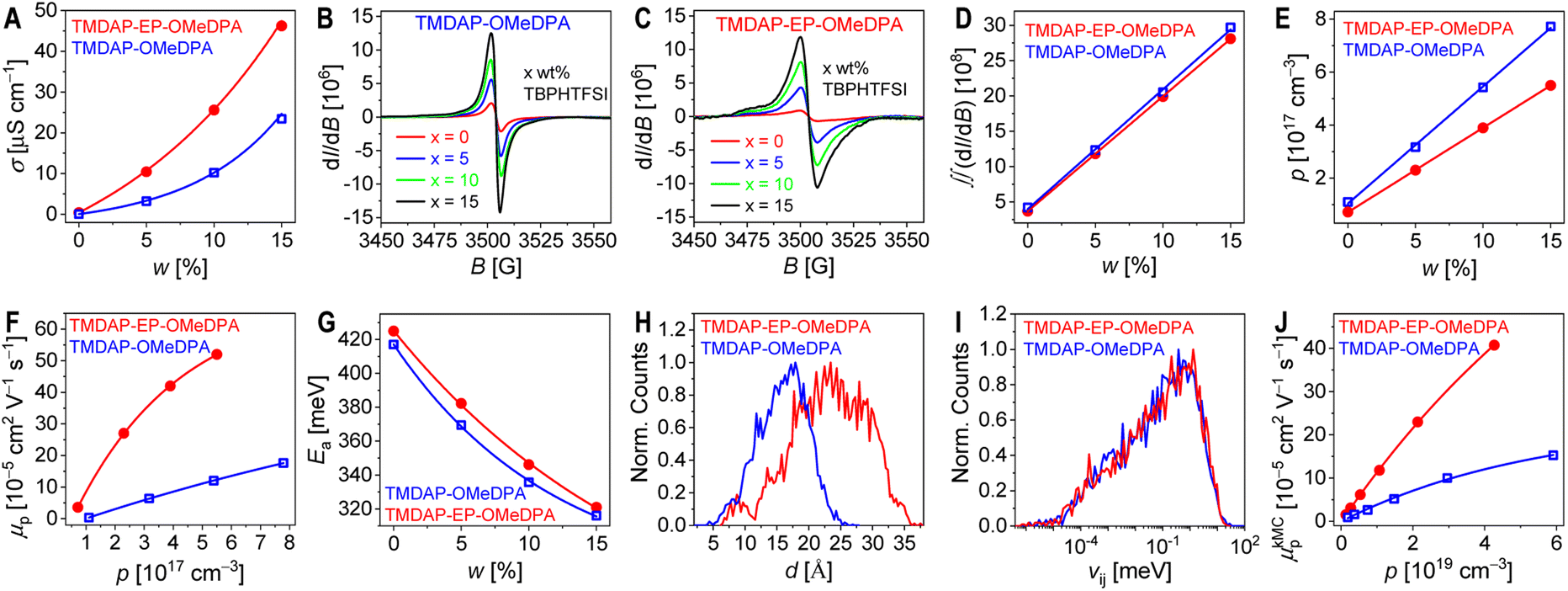 | ||
| Fig. 3 (A) Conductivity (σ) plotted as a function of the weight percentage (w) of TBPHTFSI. The solid lines represent fits based on the relationship σ ∝ wb, where b is a constant greater than 1. (B and C) Electron paramagnetic resonance spectra, showing the first derivative of absorption intensity (dI/dB) plotted against magnetic field strength (B). (D) Quadratic integral of the electron paramagnetic resonance signal plotted against the weight percentage of TBPHTFSI. The solid lines correspond to linear fits. (E) Hole density (p) plotted as a function of the weight percentage of TBPHTFSI. The solid lines represent linear fits. (F) Hole mobility (μp) plotted as a function of hole density (p). The solid lines depict monoexponential growth fits. (G) Activation energy (Ea) for hole conduction. The solid lines depict monoexponential growth fits. (H and I) Statistical analysis of two physical parameters relevant to hole transport: (H) centroid distance (d) and (I) transfer integral (vij). (J) Kinetic Monte Carlo simulated hole mobility (μkMCp) plotted against p. The solid lines correspond to monoexponential growth fits. | ||
Finally, the temperature-dependent σ of the organic semiconductor film was measured. As depicted in Fig. S4,† the σ gradually increases with temperature. By utilizing the Arrhenius equation, the activation energy for hole conduction can be determined. Fig. 3G illustrates that with an increase in the weight percentage of TBPHTFSI, the activation energy of hole conduction decreases exponentially, which indicates the shift of the Fermi energy closer to the transport level with the concomitant increase in the hole density.45 In summary, a gradual increase in the weight percentage of TBPHTFSI leads to increased p, progressively filled traps, decreased activation energy for hole transport, and a gradual improvement in μp and σ.45–47 Thereby, it is pertinent to compare the charge mobilities of organic semiconductors at the same charge density.
2.4. Microscopic insights into hole transport in organic semiconductors
In organic semiconductors, charge transport typically relies on thermal activation, with the hopping rate influenced by several factors, including the reorganization energy, the HOMO energy level difference between the hopping sites i and j, the transfer integral, and the centroid distance.48 Molecular dynamics simulations offer valuable insights into the atomic-scale microstructure of amorphous organic semiconductors, revealing a diversity of molecular conformations, orientations, and the distinct impact of surrounding electrostatic and polarization forces. In this study, we focused on dimers with nearest interatomic distances below 5 Å. Fig. 3H demonstrates a substantial difference in the average centroid distances between TMDAP-EP-OMeDPA and TMDAP-OMeDPA. Energetic disorder was determined by fitting the HOMO energy level difference in a dimer using a Gaussian function, resulting in energetic disorders of 145 meV for TMDAP-OMeDPA and 155 meV for TMDAP-EP-OMeDPA (Fig. S5†). Notably, Fig. 3I illustrates a negligible disparity in the distribution of the transfer integral. The reorganization energy for hole transport was computed via the four-point method, based on adiabatic potential energy surfaces, yielding values of 209 meV for TMDAP-OMeDPA and 147 meV for TMDAP-EP-OMeDPA. Theoretical hole mobility was simulated using the kinetic Monte Carlo method.49Fig. 3J demonstrates the exponential increase of μp in organic semiconductors as p rises. At a given p, TMDAP-EP-OMeDPA exhibits higher theoretical hole mobility than TMDAP-OMeDPA. These results are consistent with the experimental measurements.2.5. Glass transition, diffusion, and water permeation
In perovskite solar cells, the amorphous organic hole transport layer can undergo strain and/or crystallization as it approaches its glass transition temperature, resulting in reduced film uniformity, flatness, and the formation of pinholes or cracks that detrimentally affect cell efficiency. Differential scanning calorimetry measurements were conducted, revealing a glass transition temperature of 193 °C for TMDAP-OMeDPA and a higher glass transition temperature of 230 °C for TMDAP-EP-OMeDPA, which are much higher than the values of 125 °C for J4 and 121 °C for spiro-OMeTAD. However, the inclusion of 15 wt% of the small molecule TBPHTFSI induced a plasticizing effect, leading to a decrease in glass transition temperature by approximately 40 °C. Specifically, the glass transition temperature was measured to be 150 °C for the TMDAP-OMeDPA composite and 175 °C for the TMDAP-EP-OMeDPA composite, which are also remarkably higher than the values of 83 °C for the J4 composite and 72 °C for the spiro-OMeTAD composite. A higher glass transition temperature of the hole transport layer is critical to maintain the morphological stability of perovskite solar cells at elevated temperatures such as 85 °C. Molecular dynamics simulations were performed to explore the temperature-dependent specific volume characteristics. Linear fitting of the specific volume values in both the high-temperature and low-temperature regions resulted in the intersection of two lines, defining the theoretical glass transition temperature (Fig. S6†). Notably, Fig. 4A demonstrates a strong linear correlation between glass transition temperatures obtained from molecular dynamics simulation and differential scanning calorimetry measurement.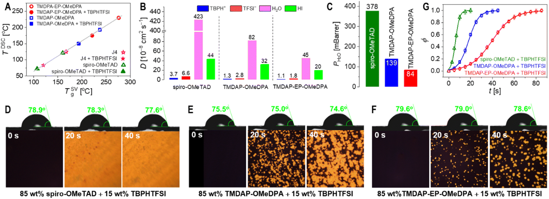 | ||
| Fig. 4 (A) Correlation between glass transition temperatures obtained from molecular dynamics simulation (TSVg) and differential scanning calorimetry measurement (TDSCg). The weight percentage of TBPHTFSI is 15%. (B) 80 °C diffusivity (D) for internal and external species in an organic semiconductor composite containing 15 wt% TBPHTFSI. (C) Water permeability (PH2O) obtained from molecular dynamics simulation for the 15 wt% TBPHTFSI-containing organic semiconductor composite. (D–F) Evolution of water contact angle (values in green) and polarized optical microscope images over time for a perovskite film covered with a hole transport layer under a water droplet. The hole transport layer composition is also provided. The polarized optical microscope image size is 500 × 500 μm. (G) Time-dependent percentage (ϕ) of the yellow region in polarized optical microscope images. | ||
Organic semiconductors doped through redox reactions inherently maintain electrostatic balance by incorporating corresponding anions and cations.50 The diffusion of some small molecules or ions in the perovskite layer and the hole transport layer, along with ion migration induced by the local electric field, can introduce variations in device parameters.51,52 For instance, the diffusion and migration of iodide ions can trigger reductive dedoping in the hole transport layer. Moreover, elevated temperature and humidity can gradually degrade the perovskite material. Effective control over the volatilization of components from the perovskite layer and the permeation of ambient moisture through the hole transport layer, which covers the perovskite surface, shows potential for enhancing the durability of perovskite solar cells.
To investigate this, we conducted molecular dynamics simulations to explore the diffusion behaviour of specific intrinsic and extrinsic species in the hole transport layer, including 4-tert-butylpyridinium (TBPH+), bis(trifluoromethanesulfonyl)imide anion (TFSI−), HI, and water. As depicted in Fig. S7,† our results demonstrate a gradual increase in the diffusivity with temperature. Specifically, at a given temperature such as 80 °C, the diffusivities of TBPH+, TFSI−, HI, and water in the TMDAP-EP-OMeDPA hole transport layer were lower compared to those in the TMDAP-OMeDPA hole transport layer (Fig. 4B). Notably, the diffusivities of these relevant species, especially water, in the spiro-OMeTAD control are significantly higher.
The water permeability exhibits a positive correlation with the diffusivity and solubility of water molecules. Molecular dynamics simulations revealed that at a weight percentage of 15% TBPHTFSI, the theoretical water permeability in the TMDAP-EP-OMeDPA and TBPHTFSI composite was 84 mBarrer, which is 1.65 times lower than that in the TMDAP-OMeDPA counterpart (water permeability = 139 mBarrer) (Fig. 4C). Notably, the water permeability in the spiro-OMeTAD control is remarkably higher, being 378 mBarrer. To visually assess water permeation, we deposited the hole transport layer onto the CsMAFA perovskite layer and subsequently applied water droplets onto its surface. As shown in Fig. 4D–F, the initial water contact angles on perovskite films covered with spiro-OMeTAD, TMDAP-OMeDPA and TMDAP-EP-OMeDPA composites were measured as 78.9°, 75.5° and 79.6°, respectively. After 40 s of water droplet deposition, the water contact angles of both samples remained essentially unchanged. Interestingly, polarized optical microscope images revealed an increasing amount of yellow birefringence over time in the region beneath water droplets, while regions without water droplets exhibited no such birefringence. Based on this observation, we speculate that in the presence of water droplets, water molecules gradually permeate into the hole transport layer, directly contacting the perovskite film, thereby leading to perovskite decomposition and the formation of discernible PbI2 grains. To quantitatively evaluate the relationship between the fraction of birefringent regions and time, we employed the mathematical expression of the Bohart–Adams fixed-bed adsorption and permeation model (Fig. 4G). Our results demonstrate that the full degradation time constant of perovskite films covered with the spiro-OMeTAD composite layer and the TMDAP-OMeDPA analogue are 20 s and 45 s, respectively, which are shorter than that of perovskite films covered with the TMDAP-EP-OMeDPA counterpart (85 s). The reciprocal ratio of the total degradation time constants is 4.3![[thin space (1/6-em)]](https://www.rsc.org/images/entities/char_2009.gif) :1.9:1, aligning well with the ratio of water permeability (4.5:1.7:1) obtained from theoretical simulations. The higher water permeabilities for the spiro-OMeTAD and TMDAP-OMeDPA composites can be attributed to the increased solubilities and diffusivities of water. Obviously, the adoption of TMDAP-EP-OMeDPA, which exhibits a lower water permeability, holds promise for impeding the penetration of external moisture, thereby effectively retarding perovskite decomposition in solar cells.
:1.9:1, aligning well with the ratio of water permeability (4.5:1.7:1) obtained from theoretical simulations. The higher water permeabilities for the spiro-OMeTAD and TMDAP-OMeDPA composites can be attributed to the increased solubilities and diffusivities of water. Obviously, the adoption of TMDAP-EP-OMeDPA, which exhibits a lower water permeability, holds promise for impeding the penetration of external moisture, thereby effectively retarding perovskite decomposition in solar cells.
2.6. Application in perovskite solar cells
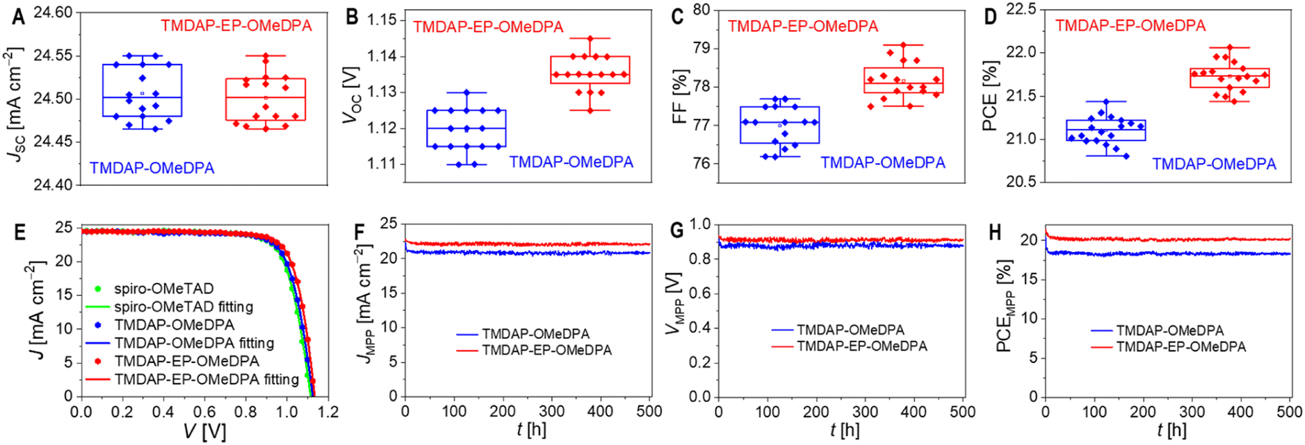 | ||
| Fig. 5 (A–D) Statistical analysis of performance parameters: (A) short-circuit photocurrent density (JSC); (B) open-circuit photovoltage (VOC); (C) fill factor (FF); (D) power conversion efficiency (PCE). (E) Representative photocurrent density–photovoltage (J–V) characteristics under the simulated AM1.5G irradiation (dotted). The solid lines refer to fits based on the Shockley diode equation. (F–H) Maximum power point (MPP) tracking results obtained under equivalent one sun irradiation from a white light emitting diode: (F) photocurrent density at MPP (JMPP); (G) photovoltage at MPP (VMPP); (H) PCE at MPP (PCEMPP). | ||
| Cell | J SC [mA cm−2] | V OC [V] | FF [%] | PCE [%] |
|---|---|---|---|---|
| a The aperture area of metal mask: 0.16 cm2. The 1000 h aging was conducted in an 85 °C oven. | ||||
| Unaged spiro-OMeTAD | 24.50 | 1.125 | 75.6 | 20.9 |
| Unaged TMDAP-OMeDPA | 24.50 | 1.120 | 77.0 | 21.1 |
| Unaged TMDAP-EP-OMeDPA | 24.50 | 1.135 | 78.2 | 21.7 |
| Aged spiro-OMeTAD | 21.70 | 1.085 | 57.9 | 13.6 |
| Aged TMDAP-OMeDPA | 22.37 | 1.115 | 60.2 | 15.0 |
| Aged TMDAP-EP-OMeDPA | 23.18 | 1.135 | 70.0 | 18.4 |
To investigate the variations in performance parameters resulting from different hole transport layers, we used the Shockley diode equation53 to fit the J–V curves, as illustrated in Fig. 5E. Additional simulations and analyses are depicted in Fig. S9 and Table S3.† Compared to the TMDAP-OMeDPA cell, the TMDAP-EP-OMeDPA cell exhibited a higher shunt resistance and a lower reverse saturation current, leading to an improved VOC. It is noteworthy that the impact of reverse saturation current on VOC is particularly significant. Furthermore, the superior FF observed in the TMDAP-EP-OMeDPA cell can be attributed to its larger shunt resistance, smaller reverse saturation current, and decreased series resistance, with the contributions ranked as series resistance > reverse saturation current > shunt resistance. The reduction in series resistance in the TMDAP-EP-OMeDPA cell is attributed to the increased conductivity of its hole transport layer. The decreased reverse saturation current and increased shunt resistance values are linked with its higher glass transition temperature, which impedes the infiltration of gold into the hole transport layer, thereby preventing filament-like contacts between the perovskite layer and the hole transport layer.
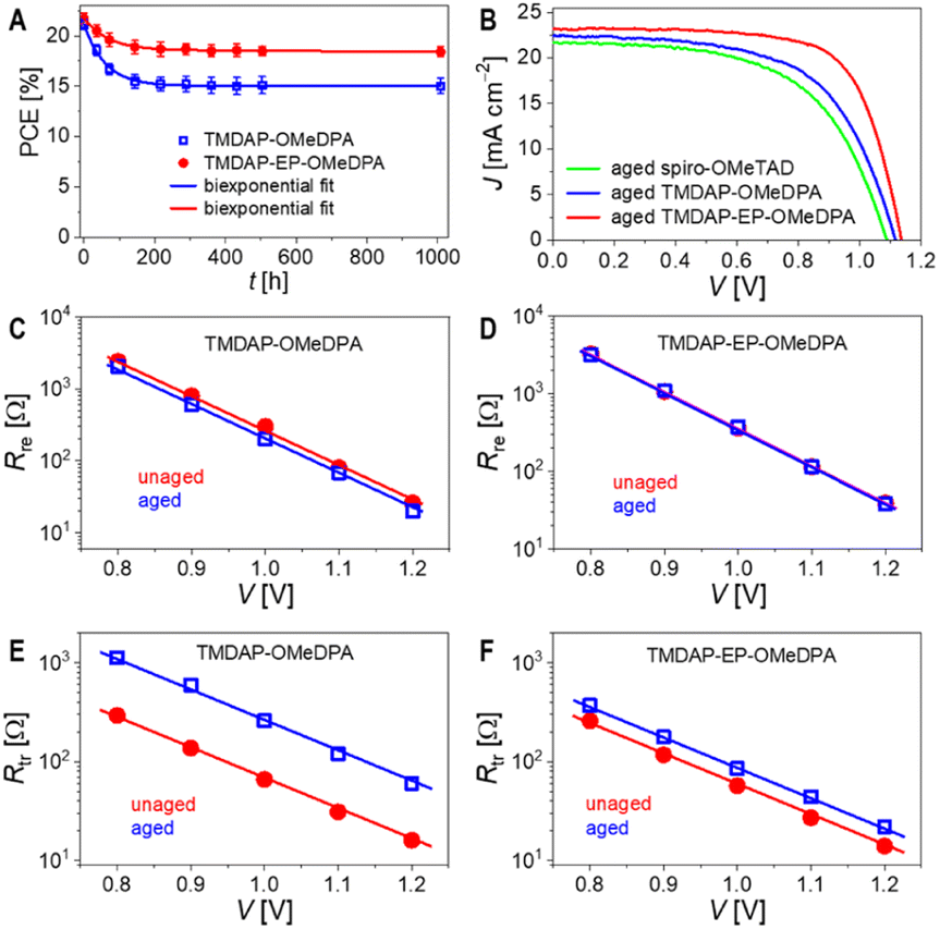 | ||
| Fig. 6 (A) Evolution of the PCE with aging time at 85 °C. (B) J–V curves under simulated AM1.5G irradiation for perovskite solar cells aged at 85 °C for 1000 h. (C and D) Plots of interface recombination resistance (Rre) as a function of voltage (V). (E and F) Plots of transport resistance (Rtr) as a function of voltage. | ||
Furthermore, we conducted measurements of the external quantum efficiency spectra of the short-circuit cells. As shown in Fig. 7A, thermal aging resulted in a reduction of the maximum external quantum efficiency for the TMDAP-OMeDPA cell from 94% to 87%. In comparison, the decrease in the maximum external quantum efficiency for the TMDAP-EP-OMeDPA cell was relatively smaller, going from 94% to 91%. By utilizing the standard AM1.5G solar spectrum (ASTM G173-03), we predicted the short-circuit photocurrent density of the cells under AM1.5G conditions (Fig. 7B). Notably, there existed a strong linear correlation between the short-circuit photocurrent density predicted from the external quantum efficiency spectra and measured from the J–V characteristics, for both the unaged and aged cells (Fig. S11†).
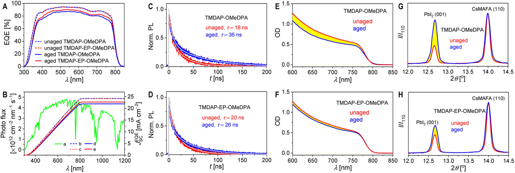 | ||
| Fig. 7 (A) External quantum efficiency (EQE) spectra of the unaged and aged perovskite solar cells. (B) ASTM G173 AM1.5G spectral photon flux (a) and the photocurrent densities predicted by the EQE spectra (JEQESC) for the unaged cell with TMDAP-OMeDPA (b), the unaged cell with TMDAP-EP-OMeDPA (c), the aged cell with TMDAP-OMeDPA (d), and the aged cell with TMDAP-EP-OMeDPA (e). (C and D) Time-resolved photoluminescence traces of the unaged and aged perovskite solar cells. The gray lines represent the biexponential fits of normalized PL as a function of time (t), yielding the amplitude-averaged lifetime (τ). (E and F) Optical densities (OD) of the unaged and aged perovskite solar cells after removal of the gold electrode. (G and H) X-ray diffraction patterns of the unaged and aged perovskite solar cells after removal of the gold electrode. X-ray diffraction intensities were normalized to the (110) plane of CsMAFA. | ||
Time-resolved photoluminescence measurements revealed a significant increase in the photoluminescence lifetime of the TMDAP-OMeDPA cell due to thermal aging, rising from 18.0 ns to 36.3 ns (Fig. 7C). In contrast, the change in photoluminescence lifetime for the TMDAP-EP-OMeDPA cell was relatively minor, with an increase from 20.0 ns to 26.1 ns (Fig. 7D). The elongation of the photoluminescence lifetime could be attributed to hole transport layer rupture and/or the formation of wide-bandgap species at the interface between the perovskite and hole transport layer. Subsequently, we removed the encapsulation material and gold electrode to measure the electronic absorption spectra of the cells before and after aging. Fig. 7E and F indicate a reduction in optical density within the 600–800 nm wavelength range for the aged cells, signifying perovskite photoactive layer decomposition. The TMDAP-EP-OMeDPA cell exhibited a smaller decrease in light absorption compared to the TMDAP-OMeDPA cell. Additionally, X-ray diffraction patterns were recorded (Fig. 7G and H). The peak centered at 2θ = 14.0° corresponded to diffraction from the (110) crystal plane of the α-phase perovskite, while the peak centered at 2θ = 12.7° could be attributed to the (001) diffraction of PbI2. Notably, the PbI2 (001) diffraction peak was observed even in the unaged cells due to excess PbI2 in the precursor solution during perovskite deposition. Aging at 85 °C resulted in perovskite degradation and the formation of wide-bandgap species, PbI2. The increase in PbI2 diffraction intensity was significantly greater for the TMDAP-OMeDPA cell compared to the TMDAP-EP-OMeDPA cell.
Furthermore, scanning electron microscope tests were conducted to examine the morphological changes of the hole transport layers in perovskite solar cells before and after aging. As depicted in Fig. 8A and B, the hole transport layers in the unaged cells uniformly covered the perovskite polycrystalline layer. Following 1000 hours of aging, the hole transport layer in the TMDAP-OMeDPA cell exhibited a highly rough texture with penetrating fractures (Fig. 8C, highlighted by yellow circles), while the hole transport layer in the TMDAP-EP-OMeDPA cell displayed slight roughness with shallow pits (Fig. 8D). Deterioration in hole transport layer morphology can compromise hole extraction and transport, and in severe cases, it may lead to localized contact between the perovskite layer and the gold electrode. Subsequently, the hole transport layers were removed using chlorobenzene, and the surface morphology of the perovskite layer was examined. Scanning electron microscope images of the perovskite layers in the unaged cells (Fig. 8E and F) revealed a tightly packing of sub-micron-sized grains. Upon thermal aging, numerous sub-micron-sized voids emerged in the perovskite layer of the TMDAP-OMeDPA cell (Fig. 8G, indicated by yellow circles), while the morphology of the perovskite layer in the aged TMDAP-EP-OMeDPA cell exhibited minimal change (Fig. 8H).
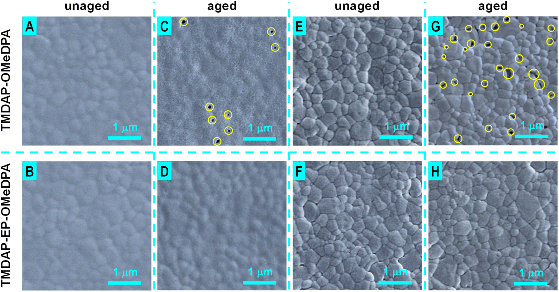 | ||
| Fig. 8 (A–D) Top-view scanning electron microscope images for the hole transport layers in the unaged and aged perovskite solar cells. The encapsulation material and the gold electrode were removed prior to imaging. (E–H) Top-view scanning electron microscope images for the perovskite layers in the unaged and aged perovskite solar cells. The encapsulation material, the gold electrode, and the hole transport layers were removed prior to imaging. | ||
Additionally, fluorescence optical microscope measurements indicated the absence of discernible microstructures in the perovskite layers of the unaged cells (Fig. 9A and B). Conversely, in the aged TMDAP-OMeDPA cell, the perovskite layer displayed densely distributed needle-shaped or punctate species emitting green light (Fig. 9C), which we attributed to the G-band emission of PbI2. In comparison, the perovskite layer of the aged TMDAP-EP-OMeDPA cell only exhibited punctate species (Fig. 9D). The results obtained from electronic absorption, X-ray diffraction, scanning electron microscope, and fluorescence optical microscope measurements suggest that, in comparison to TMDAP-OMeDPA, the utilization of TMDAP-EP-OMeDPA can not only maintain the hole transport layer morphology but also retard the thermal degradation of the organic–inorganic hybrid halide perovskite.
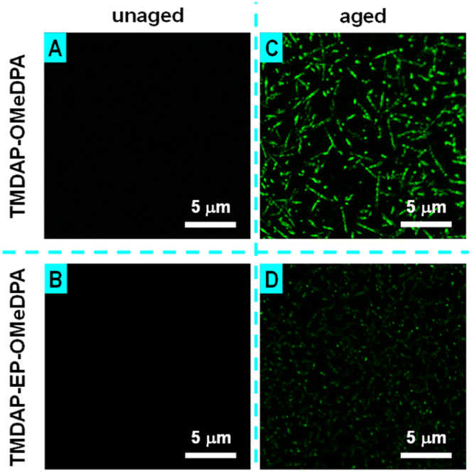 | ||
| Fig. 9 (A–D) Fluorescence optical microscope images for the perovskite layers in the unaged and aged perovskite solar cells. The encapsulation material, the gold electrode, and the hole transport layers were removed prior to imaging. | ||
3. Conclusions
In summary, we have successfully synthesized a trimethylated, nonplanar polycyclic heteroaromatic, which features two aza[5]helicenes bridged by pyrrole (TMDAP). Through the incorporation of electron donors, we have developed two TMDAP-based organic semiconductors with sufficiently high HOMO energy levels for use in perovskite solar cells. Notably, compared to the bis(4-methoxyphenyl)amine electron donor, EP-OMeDPA enhanced the hole mobility of the TMDAP-based organic semiconductors by one order of magnitude, under an identical hole density. This improvement can be attributed to reduced reorganization energy and increased average centroid distance, despite having comparable transfer integrals and slightly increased energetic disorder. Consequently, when employed as the doped hole transport layer in perovskite solar cells with a triple cation lead halide perovskite, TMDAP-EP-OMeDPA demonstrated superior PCEs of up to 22.1%. Moreover, TMDAP-EP-OMeDPA exhibited a higher glass transition temperature and lower diffusivity for external small molecules and ions compared to TMDAP-OMeDPA. These essential, yet uncommon, properties of an organic semiconductor contributed to enhanced long-term operational stability and improved thermostability for perovskite solar cells. Detailed analysis of device degradation highlighted the significance of utilizing an organic semiconductor with a high glass transition temperature to preserve the morphology of the hole transport layer and mitigate the degradation of the hybrid perovskite layer. Overall, our study provides valuable insights into the design of high-performance organic semiconductors for achieving efficient and durable perovskite solar cells.Data availability
All the data supporting this article have been included in the main text and the ESI.†Author contributions
Conceptualization: P. W. Data curation: Y. W.; Y. C. Funding acquisition: Y. Y.; P. W. Investigation: Y. W.; Y. C.; L. H.; Y. Z.; J. Z. Methodology: Y. W.; J. Z. Project administration: J. Z.; Y. Y. Supervision: Y. Y. Validation: Y. Z. Visualization: Y. W.; J. Z. Writing – original draft: Y. W.; Y. Y. Writing – review & editing: P. W.Conflicts of interest
There are no conflicts to declare.Acknowledgements
We thank the financial support from the National Natural Science Foundation of China (52073250 and 22275160), the National Key Research and Development Program of China (2022YFA1204800), and the Science and Technology Innovation Program of Hunan Province (No. 2021RC5009).Notes and references
- V. Coropceanu, J. Cornil, D. A. da Silva Filho, Y. Olivier, R. Silbey and J.-L. Brédas, Chem. Rev., 2007, 107, 926 CrossRef CAS PubMed.
- P. M. Beaujuge and J. M. J. Fréchet, J. Am. Chem. Soc., 2011, 133, 20009 CrossRef CAS PubMed.
- Z. B. Henson, K. Müllen and G. C. Bazan, Nat. Chem., 2012, 4, 699 CrossRef CAS PubMed.
- J. Mei, Y. Diao, A. L. Appleton, L. Fang and Z. Bao, J. Am. Chem. Soc., 2013, 135, 6724 CrossRef CAS PubMed.
- S. Fratini, M. Nikolka, A. Salleo, G. Schweicher and H. Sirringhaus, Nat. Mater., 2020, 19, 491 CrossRef CAS PubMed.
- H. Bässler and A. Köhler, Top. Curr. Chem., 2012, 312, 1 Search PubMed.
- A. D. Scaccabarozzi, A. Basu, F. Aniés, J. Liu, O. Zapata-Arteaga, R. Warren, Y. Firdaus, M. I. Nugraha, Y. Lin, M. Campoy-Quiles, N. Koch, C. Müller, L. Tsetseris, M. Heeney and T. D. Anthopoulos, Chem. Rev., 2022, 122, 4420 CrossRef CAS PubMed.
- J. Burschka, N. Pellet, S.-J. Moon, R. Humphry-Baker, P. Gao, M. K. Nazeeruddin and M. Grätzel, Nature, 2013, 499, 316 CrossRef CAS PubMed.
- Q. Jiang, Y. Zhao, X. Zhang, X. Yang, Y. Chen, Z. Chu, Q. Ye, X. Li, Z. Yin and J. You, Nat. Photonics, 2019, 13, 460 CrossRef CAS.
- J. Park, J. Kim, H.-S. Yun, M. J. Paik, E. Noh, H. J. Mun, M. G. Kim, T. J. Shin and S. I. Seok, Nature, 2023, 616, 724 CrossRef CAS PubMed.
- J. Salbeck, N. Yu, J. Bauer, F. Weissörtel and H. Bestgen, Synth. Met., 1997, 91, 209 CrossRef CAS.
- U. Bach, D. Lupo, P. Comte, J. E. Moser, F. Weissörtel, J. Salbeck, H. Spreitzer and M. Grätzel, Nature, 1998, 395, 583 CrossRef CAS.
- X. Zhao, H.-S. Kim, J.-Y. Seo and N.-G. Park, Mater. Interfaces, 2017, 9, 7148 CrossRef CAS PubMed.
- Y. Ren, M. Ren, X. Xie, J. Wang, Y. Cai, Y. Yuan, J. Zhang and P. Wang, Nano Energy, 2021, 81, 105655 CrossRef CAS.
- J. E. Anthony, Angew. Chem., Int. Ed., 2008, 47, 452 CrossRef CAS PubMed.
- X. Zhan, A. Facchetti, S. Barlow, T. J. Marks, M. A. Ratner, M. R. Wasielewski and S. R. Marder, Adv. Mater., 2011, 23, 268 CrossRef CAS PubMed.
- M. Stępień, E. Gońka, M. Żyła and N. Sprutta, Chem. Rev., 2017, 117, 3479 CrossRef PubMed.
- X.-Y. Wang, X. Yao, A. Narita and K. Müllen, Acc. Chem. Res., 2019, 52, 2491 CrossRef CAS PubMed.
- R. H. Martin, Angew. Chem., Int. Ed., 1974, 13, 649 CrossRef.
- Y. Shen and C.-F. Chen, Chem. Rev., 2012, 112, 1463 CrossRef CAS PubMed.
- M. Gingras, Chem. Soc. Rev., 2013, 42, 1051 RSC.
- T. Mori, Chem. Rev., 2021, 121, 2373 CrossRef CAS PubMed.
- J. Meisenheimer and K. Witte, Chem. Ber., 1903, 36, 4153 CrossRef CAS.
- W. Fuchs and F. Niszel, Ber. Dtsch. Chem. Ges., 1927, 60, 209 CrossRef.
- M. S. Newman, W. B. Lutz and D. A. Lednicer, J. Am. Chem. Soc., 1955, 77, 3420 CrossRef CAS.
- C. Kim, T. J. Marks, A. Facchetti, M. Schiavo, A. Bossi, S. Maiorana, E. Licandro, F. Todescato, S. Toffanin, M. Muccini, C. Graiff and A. Tiripicchio, Org. Electron., 2009, 10, 1511 CrossRef CAS.
- S. Sahasithiwat, T. Mophuang, L. Menbangpung, S. Kamtonwong and T. Sooksimuang, Synth. Met., 2010, 160, 1148 CrossRef CAS.
- Y. Yang, R. C. da Costa, M. J. Fuchter and A. J. Campbell, Nat. Photonics, 2013, 7, 634 CrossRef CAS.
- K. Nakahara, C. Mitsui, T. Okamoto, M. Yamagishi, K. Miwa, H. Sato, A. Yamano, T. Uemura and J. Takeya, Chem. Lett., 2013, 42, 654 CrossRef CAS.
- L. Shan, D. Liu, H. Li, X. Xu, B. Shan, J.-B. Xu and Q. Miao, Adv. Mater., 2015, 27, 3418 CrossRef CAS PubMed.
- Y. Zhong, M. T. Trinh, R. Chen, G. E. Purdum, P. P. Khlyabich, M. Sezen, S. Oh, H. Zhu, B. Fowler, B. Zhang, W. Wang, C.-Y. Nam, M. Y. Sfeir, C. T. Black, M. L. Steigerwald, Y.-L. Loo, F. Ng, X.-Y. Zhu and C. Nuckolls, Nat. Commun., 2015, 6, 8242 CrossRef CAS PubMed.
- E. Castro, T. J. Sisto, E. L. Romero, F. Liu, S. R. Peurifoy, J. Wang, X. Zhu, C. Nuckolls and L. Echegoyen, Angew. Chem., Int. Ed., 2017, 56, 14648 CrossRef CAS PubMed.
- Y.-S. Lin, S. Y. Abate, K.-W. Lai, C.-W. Chu, Y.-D. Lin, Y.-T. Tao and S.-S. Sun, ACS Appl. Mater. Interfaces, 2018, 10, 41439 CrossRef CAS PubMed.
- N. Xu, Y. Li, D. Ricciarelli, J. Wang, E. Mosconi, Y. Yuan, F. De Angelis, S. M. Zakeeruddin, M. Grätzel and P. Wang, iScience, 2019, 15, 234 CrossRef CAS PubMed.
- N. Xu, A. Zheng, Y. Wei, Y. Yuan, J. Zhang, M. Lei and P. Wang, Chem. Sci., 2020, 11, 3418 RSC.
- J. Wang, H. Shi, N. Xu, J. Zhang, Y. Yuan, M. Lei, L. Wang and P. Wang, Adv. Funct. Mater., 2020, 30, 2002114 CrossRef CAS.
- J. Vailassery and S.-S. Sun, Molecules, 2023, 28, 510 CrossRef CAS PubMed.
- C. M. Cardona, W. Li, A. E. Kaifer, D. Stockdale and G. C. Bazan, Adv. Mater., 2011, 23, 2367 CrossRef CAS PubMed.
- M. Saliba, T. Matsui, J.-Y. Seo, K. Domanski, J.-P. Correa-Baena, M. K. Nazeeruddin, S. M. Zakeeruddin, W. Tress, A. Abate, A. Hagfeldt and M. Grätzel, Energy Environ. Sci., 2016, 9, 1989 RSC.
- H. J. Snaith and M. Grätzel, Appl. Phys. Lett., 2006, 89, 262114 CrossRef.
- J. Simon and P. Bassoul, Design of Molecular Materials: Supramolecular Engineering, Wiley, 2000 Search PubMed.
- T. W. Barrett, H. Wobltjen and A. Snow, Nature, 1983, 301, 694 CrossRef CAS.
- E. J. Meijer, C. Detcheverry, P. J. Baesjou, E. van Veenendaal, D. M. de Leeuw and T. M. Klapwijk, J. Appl. Phys., 2003, 93, 4831 CrossRef CAS.
- S. Mehraeen, V. Coropceanu and J.-L. Brédas, Phys. Rev. B, 2013, 87, 195209 CrossRef.
- S. Olthof, S. Mehraeen, S. K. Mohapatra, S. Barlow, V. Coropceanu, J.-L. Brédas, S. R. Marder and A. Kahn, Phys. Rev. Lett., 2012, 109, 176601 CrossRef PubMed.
- D. Kiefer, R. Kroon, A. I. Hofmann, H. Sun, X. Liu, A. Giovannitti, D. Stegerer, A. Cano, J. Hynynen, L. Yu, Y. Zhang, D. Nai, T. F. Harrelson, M. Sommer, A. J. Moulé, M. Kemerink, S. R. Marder, I. McCulloch, M. Fahlman, S. Fabiano and C. Müller, Nat. Mater., 2019, 18, 149 CrossRef CAS PubMed.
- M. Schwarze, C. Gaul, R. Scholz, F. Bussolotti, A. Hofacker, K. S. Schellhammer, B. Nell, B. D. Naab, Z. Bao, D. Spoltore, K. Vandewal, J. Widmer, S. Kera, N. Ueno, F. Ortmann and K. Leo, Nat. Mater., 2019, 18, 242 CrossRef CAS PubMed.
- J. L. Brédas, J. P. Calbert, D. A. da Silva Filho and J. Cornil, Proc. Natl. Acad. Sci. U. S. A., 2002, 99, 5804 CrossRef PubMed.
- V. Rühle, A. Lukyanov, F. May, M. Schrader, T. Vehoff, J. Kirkpatrick, B. Baumeier and D. Andrienko, J. Chem. Theory Comput., 2011, 7, 3335 CrossRef PubMed.
- I. Salzmann, G. Heimel, M. Oehzelt, S. Winkler and N. Koch, Acc. Chem. Res., 2016, 49, 370 CrossRef CAS PubMed.
- C. C. Boyd, R. Cheacharoen, T. Leijtens and M. D. McGehee, Chem. Rev., 2019, 119, 3418 CrossRef CAS PubMed.
- S. P. Dunfield, L. Bliss, F. Zhang, J. M. Luther, K. Zhu, M. F. A. M. van Hest, M. O. Reese and J. J. Berry, Adv. Energy Mater., 2020, 10, 1904054 CrossRef CAS.
- S. Yoo, B. Domercq and B. Kippelen, J. Appl. Phys., 2005, 97, 103706 CrossRef.
- V. Gonzalez-Pedro, E. J. Juarez-Perez, W.-S. Arsyad, E. M. Barea, F. Fabregat-Santiago, I. Mora-Sero and J. Bisquert, Nano Lett., 2014, 14, 888 CrossRef CAS PubMed.
Footnote |
| † Electronic supplementary information (ESI) available. CCDC 2195841. For ESI and crystallographic data in CIF or other electronic format see DOI: https://doi.org/10.1039/d3sc02845c |
| This journal is © The Royal Society of Chemistry 2023 |