
 Open Access Article
 This Open Access Article is licensed under a Creative Commons Attribution-Non Commercial 3.0 Unported Licence
Pt cocatalyst morphology on semiconductor nanorod photocatalysts enhances charge trapping and water reduction†
Bumjin
Park‡
 a,
Won-Woo
Park‡
b,
Ji Yong
Choi‡§
a,
Woong
Choi¶
a,
Young Mo
Sung
c,
Soohwan
Sul
*c,
Oh-Hoon
Kwon
*b and
Hyunjoon
Song
*a
a,
Won-Woo
Park‡
b,
Ji Yong
Choi‡§
a,
Woong
Choi¶
a,
Young Mo
Sung
c,
Soohwan
Sul
*c,
Oh-Hoon
Kwon
*b and
Hyunjoon
Song
*a
aDepartment of Chemistry, Korea Advanced Institute of Science and Technology, Daejeon 34141, Republic of Korea. E-mail: hsong@kaist.ac.kr
bDepartment of Chemistry, Ulsan National Institute of Science and Technology, Ulsan 44919, Republic of Korea. E-mail: ohkwon@unist.ac.kr
cAnalytical Engineering Group, Samsung Advanced Institute of Technology, Samsung Electronics Co., Ltd, Suwon 16678, Republic of Korea. E-mail: soohwan.sul@samsung.com
First published on 23rd June 2023
Abstract
In photocatalysis, metal–semiconductor hybrid structures have been proposed for ideal photocatalytic systems. In this study, we investigate the effect of morphology and surface nature of Pt cocatalysts on photocatalytic hydrogen evolution activity in Pt-tipped CdSe nanorods. Three distinct morphologies of Pt cocatalysts were synthesized and employed as visible light photocatalysts. The rough tips exhibit the highest activity, followed by the round and cubic tips. Kinetic investigations using transient absorption spectroscopy reveal that the cubic tips exhibit lower charge-separated states feasible for reacting with water and water reduction rates due to their defectless surface facets. In contrast, the rough tips show a similar charge-separation value but a two-fold higher surface reaction rate than the round tips, resulting in a significant enhancement of hydrogen evolution. These findings highlight the importance of rational design on metal cocatalysts in addition to the main semiconductor bodies for maximizing photocatalytic activities.
Introduction
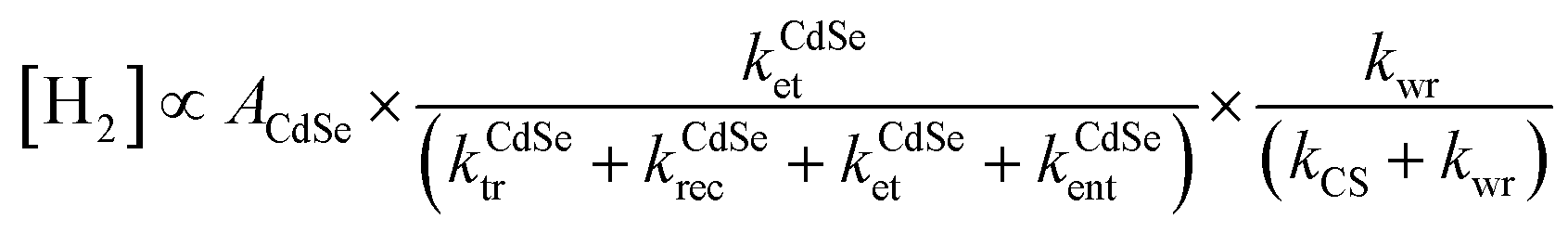
Solar fuels, chemical fuels converted by renewable energy resources originating from solar energy, are becoming primary topics for establishing a clean energy system to resolve the current energy and environmental problems.1 One of the most promising solar fuels is hydrogen gas, which has a wide range of applications, including fuel cells, hydrogen vehicles, and industrial processes.2 Among the various methods for hydrogen production from aqueous protons, photocatalytic pathways are considered an ultimate goal due to their ability to utilize sunlight directly.3 Since Honda et al. observed the photocatalytic effect of semiconducting materials, semiconductor catalysts combined with metal cocatalysts have been proposed as an ideal configuration for achieving efficient photoinduced carrier transfer to metal domains in photocatalytic hydrogen production.4–7This ideal structure may appear simple, with only two distinct domains. However, its photophysical kinetics are exceedingly complicated, including processes such as light absorption, charge-separated (CS) state formation, carrier/exciton transfer and recombination, trapping at surface traps, and water reduction on active sites.3,5 For instance, in the Pt–CdSe cocatalyst–catalyst system (Scheme 1a), the band diagram illustrates a complex profile consisting of multiple independent kinetic parameters for hydrogen evolution (Scheme 1b).7 The hydrogen evolution rate is deduced from a series of kinetic equations when the water reduction rate is slower than the others (see ESI†):
 | (1) |
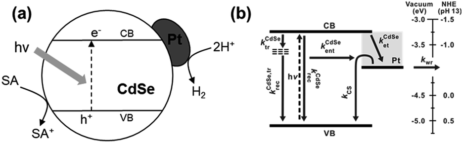 | ||
| Scheme 1 (a) A representative scheme of the Pt–CdSe photocatalyst structure for hydrogen evolution (SA: sacrificial agent) and (b) corresponding band diagram.7 | ||
These carrier transfer and relaxation kinetics are closely correlated; thus, it is challenging to estimate each parameter precisely. In this respect, introducing simplified model catalysts can effectively decouple the critical factors and provide vital information for analyzing catalytic behaviors. Metal-tipped semiconductor nanorods are well-defined model catalyst systems for this purpose.8 In eqn (1), the first term, the light absorption of the rods (ACdSe), could be modulated by alloy semiconductors, Zn1−xCdxSe, with different metal ratios (x = 0–1). In Pt-tipped nanorods, however, electron mobility toward the Pt tip was another critical factor in enhancing hydrogen evolution.9 For Pt–CdSe nanorods, elongation of the rods increased the absorption cross-section (ACdSe) but significantly reduced the electron transfer rate to the Pt tips (kCdSeet) in the second term, leading to an optimal geometry of the tipped nanorods with 15–20 nm length.7
The morphology and composition of the metal cocatalyst also play a crucial role in determining the overall efficiency of the reaction,10–12 as depicted in the third term of eqn (1). Au tips showed slower recombination of the CS state, while Pt tips exhibited higher kwr. As a result, the combination of Au and Pt as a core–shell structure at the tip induced the maximum hydrogen evolution rate.10 Additionally, the size of the cocatalyst has been found to be a critical factor, with cocatalyst sizes in the range of 3 nm in Pt–CdS nanorods showing a high quantum efficiency due to improved charge separation and water reduction efficiencies.12 However, the effects of morphology and surface structure on the metal cocatalysts have not been widely studied in the context of photocatalysis, despite their critical impact on numerous catalytic reactions.13 Defect engineering in semiconductors has been shown to affect the adsorption of water molecules and protons, as well as the trapping of electrons,14,15 which suggests that similar effects may also occur in the morphology of metal cocatalysts.
In this study, we investigate the effect of Pt cocatalyst morphology on the photocatalytic hydrogen evolution rate in CdSe nanorods. Three distinct morphologies of Pt cocatalysts – round, cubic, and rough – were synthesized at the tips of otherwise identical CdSe nanorods. Photochemical hydrogen evolution experiments showed that the rough tips exhibited a six-fold higher reaction rate than the cubic sample. Through comprehensive kinetic analyses, we demonstrate that the rational design of metal cocatalyst morphology can influence carrier dynamics and water reduction rates, leading to a significant enhancement of photocatalytic activity.
Results and discussion
CdSe nanorods were selected as a model semiconductor catalyst due to their single-crystalline nature and precisely controllable aspect ratio. The CdSe nanorods were uniformly prepared with an average length of 17.4 ± 1.6 nm and a diameter of 5.6 ± 0.5 nm (Fig. S1, ESI†), targeting the optimal geometry of CdSe–Pt nanorod catalysts in hydrogen evolution reactions.7 Thermal decomposition of Pt precursors in the presence of surface regulating reagents induced Pt tip growth on the nanorods with specific morphology. Defect-mediated growth on the heterogeneous CdSe surface induced selective formation on the nanorod tips under the low concentration of the Pt precursors.8,16 Round tips were grown in a mixture of hexadecanediol, oleylamine, and oleic acid.7,8 For cubic tips, bubbling CO into the reaction mixture effectively suppressed the growth along 〈100〉 by preferential coordination,17 and led to formation of cubic morphology. For rough tips, bulky ligands such as 1-adamantanecarboxylic acid were added to protect active surface sites.18,19 As a result, anisotropic growth was induced to generate rough tips with multiple bumps. The atomic ratio of Pt was kept constant as 35–40% of the total heavy elements, measured by inductively coupled plasma-atomic emission spectroscopy (ICP-AES; Table S1, ESI†).The transmission electron microscopy (TEM) images show that Pt–CdSe nanorods were uniformly produced (Fig. 1). Statistical analysis reveals the distribution of double-tipped (or dumbbells, 64–70%), single-tipped (or matchsticks, 28–34%), and bare nanorods (3–5%) for the three distinct morphologies (Fig. S2, ESI†). These similar structural distributions allow for comparing photochemical reactivity. The CdSe nanorods with round tips (Round) have a tip morphology with smoother surfaces than the other tip structures (Fig. 1a). In the high-resolution TEM (HRTEM) images, CdSe nanorods are single-crystalline with a growth direction along 〈002〉. A single-crystalline Pt particle with a round morphology is attached to the nanorod tip. The nanorods with cubic tips (Cubic) have flat surface faces with sharp edges on the Pt tips (Fig. 1b). Each cubic tip has lattice fringes parallel to the (100) faces. The average distance between the neighboring fringes matches the Pt(200) lattice constant, 0.196 nm, indicative of cubic morphology. The nanorods with rough tips (Rough) show irregular curved surfaces on the Pt tips. In the HRTEM image, however, the lattice fringes corresponding to Pt(111) and (200) cover all particle ranges, revealing the single-crystalline nature (Fig. 1c).
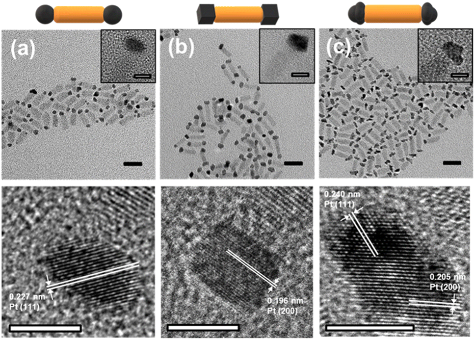 | ||
| Fig. 1 TEM and HRTEM images of (a) Round, (b) Cubic, and (c) Rough. The bars represent (TEM images) 20 nm and (inset and HRTEM images) 5 nm. | ||
The X-ray diffraction (XRD) data display a linear combination between hexagonal wurtzite CdSe (JCPDS No. 08-0459) and face-centered cubic Pt (JCPDS No. 04-0802) patterns (Fig. S3, ESI†).8 The UV-visible absorption spectrum of the bare CdSe nanorods exhibits an intense absorption peak centered at 640 nm, assigned to the first excitonic transition (1σv → 1σc) from the valence band to the conduction band edges (Fig. 2a).20 After the Pt deposition, these apparent peaks are broadened due to delocalization of the electronic states of the semiconductor into the metal domains.10 In addition, a contribution from the absorption of Pt tips increases total absorbance in a wide wavelength range. Similar patterns of the absorption spectra indicate that the amounts of Pt atoms deposited on the nanorods are nearly identical for all samples. The photoluminescence (PL) spectrum of the bare CdSe nanorods has an intense peak at 650 nm, but all Pt–CdSe nanorods undergo nearly complete quenching (Fig. 2b). This reveals that electron transfer effectively occurs from the CdSe domains to the Pt tips regardless of their morphology.7
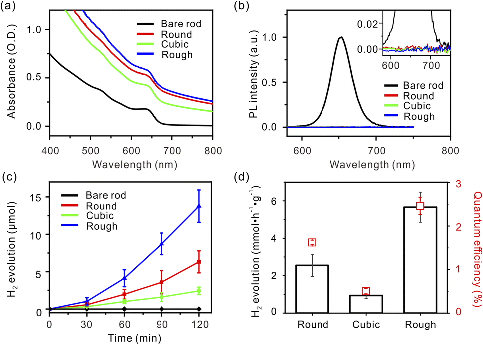 | ||
| Fig. 2 (a) UV-visible absorption and (b) PL spectra of bare nanorods, Round, Cubic, and Rough dispersed in toluene (inset: magnified PL spectra showing complete electron quenching on the CdSe domain of the Pt-tipped nanorods). (c) Temporal reaction progress and (d) photocatalytic activity under visible light irradiation (λ ≥ 420 nm) (black bars) and quantum efficiency with the excitation at 420 nm (red squares) of Round, Cubic, and Rough in a 0.35 M Na2SO3/0.25 M Na2S aqueous solution. | ||
Based on the optical behaviors in the visible region, three Pt–CdSe nanorods, Round, Cubic, and Rough, were employed as photocatalysts for hydrogen evolution from water. The surfactants were exchanged with mercaptoundecanoic acid, and the resulting catalysts were dispersed in a 0.35 M Na2SO3/0.25 M Na2S aqueous solution.8,21 The catalyst amount was fixed at 1.5 mg for all catalysts, as confirmed by ICP-AES. Under visible light irradiation (λ ≥ 420 nm), hydrogen was continuously produced (Fig. 2c). The production rates were highly dependent upon the Pt cocatalyst morphology. After an induction period of 30 min, the reaction rate reached a constant value for each catalyst. For Cubic, the infrared spectrum indicated that the CO ligands were effectively removed during the induction period (Fig. S4, ESI†).22,23 The hydrogen evolution activity was measured to be in the order of Rough (5.66 mmol h−1 g−1) > Round (2.55 mmol h−1 g−1) > Cubic (0.94 mmol h−1 g−1) (Fig. 2d, black). When irradiated by the 420 nm light using a light-emitting diode, the quantum yield of hydrogen evolution was estimated to be 2.46% for Rough, 1.62% for Round, and 0.51% for Cubic, respectively, showing the same trend as the reaction rates (Fig. 2d, red). It is remarkable that Rough exhibits six times larger activity and quantum efficiency than Cubic, although all other structural parameters except the Pt morphology are identical. The photocatalytic stability of Rough was evaluated by four cycles of a 2 h-reaction after N2 purging (Fig. S5, ESI†). The reaction rate increased upon repeating the cycle, revealing effective surface activation during the photochemical reactions.
Numerous reports have shown that the catalyst morphology and surface structure are essential factors dominating catalytic performances in nanostructured systems.13,24–28 We measured photoelectrochemical responses to elucidate the trend of photocatalytic properties (Fig. S6, ESI†). The catalysts were deposited onto a fluorine-doped tin oxide (FTO) electrode as a working electrode in a three-electrode photochemical cell. The photocurrent was measured at an applied potential of −0.5 V vs. Ag/AgCl in a 0.35 M Na2SO3/0.25 M Na2S solution. The resulting photocurrent density was in the order of Rough > Round > Cubic, following the hydrogen evolution rate in the reaction study. This revealed that the charge separation was related to the reaction rate.10 From the third term of eqn (1), it is rational to consider that the charge carrier dynamics, particularly kCS, is closely related to the cocatalyst morphology, as well as the surface reaction rate, kwr. The Nyquist plots of the catalysts also indicated that Rough exhibited enhanced charge separation and reduced recombination rates than the other samples (Fig. S7, ESI†).
To correlate the essential carrier generation and relaxation dynamics with the catalytic efficiency more precisely, we carried out transient absorption (TA) spectroscopy.29–31 For semiconductor–metal hybrid systems, electron transfer has been reported to occur in a time range of a hundred femtoseconds.7,29,32 Ultrafast energy transfer and short-lived back electron transfer (recombination) occur on a similar timescale of electron transfer and, thus, are the keys for determining the extent of the electron transfer to the metal domain, i.e., the formation of a CS state.7,32 The resulting CS state in the hybrid system shows much slower relaxation than exciton dynamics in bare CdSe nanorods.7,32 When the semiconductor rod length was the only factor to control the carrier transfer process to the metal tip, the relaxation rate of the CS state, kCS, was observed to be independent of the rod length.7
Upon photoexcitation, the TA spectra of both bare and tipped nanorods show negative absorption bands centered at ∼645 nm, corresponding to the immediate bleaching of the first excitonic transition (XB) band of CdSe (Fig. 3a and b). For the bare nanorods, the XB band bleaches further and bathochromically shifts to 210 fs, owing to the intra-band relaxation of hot carriers to the band edge (Fig. S11, ESI†).33 Then, it recovers multi-exponentially, mainly in the nanosecond timescale (Table S2, ESI†). For the Pt–CdSe nanorods, the majority of XB recovers within several hundred femtoseconds (Fig. 3b, S6, and Table S2, ESI†). Approximately 10 ps after excitation, the XB band narrows and hypsochromically shifts. In addition, unique positive photoinduced absorption (PIA) bands on both sides of the XB band appear in a peak–dip–peak shape. These bands are evidence of new transient species evolving during the electron transfer, which are not observed for the bare nanorods. The transient species were found to exist much longer than our time window of 3 ns for the femtosecond-resolved TA measurements. To resolve the ultraslow dynamics, we measured nanosecond-resolved TA spectra (Fig. S10, ESI†). The Pt–CdSe nanorods also show the peak–dip–peak-shape TA spectra on the microsecond timescale (Table S3, ESI†). In contrast, for the bare nanorods, the excitons fully relax within sub-microseconds (Fig. S10, ESI†).7
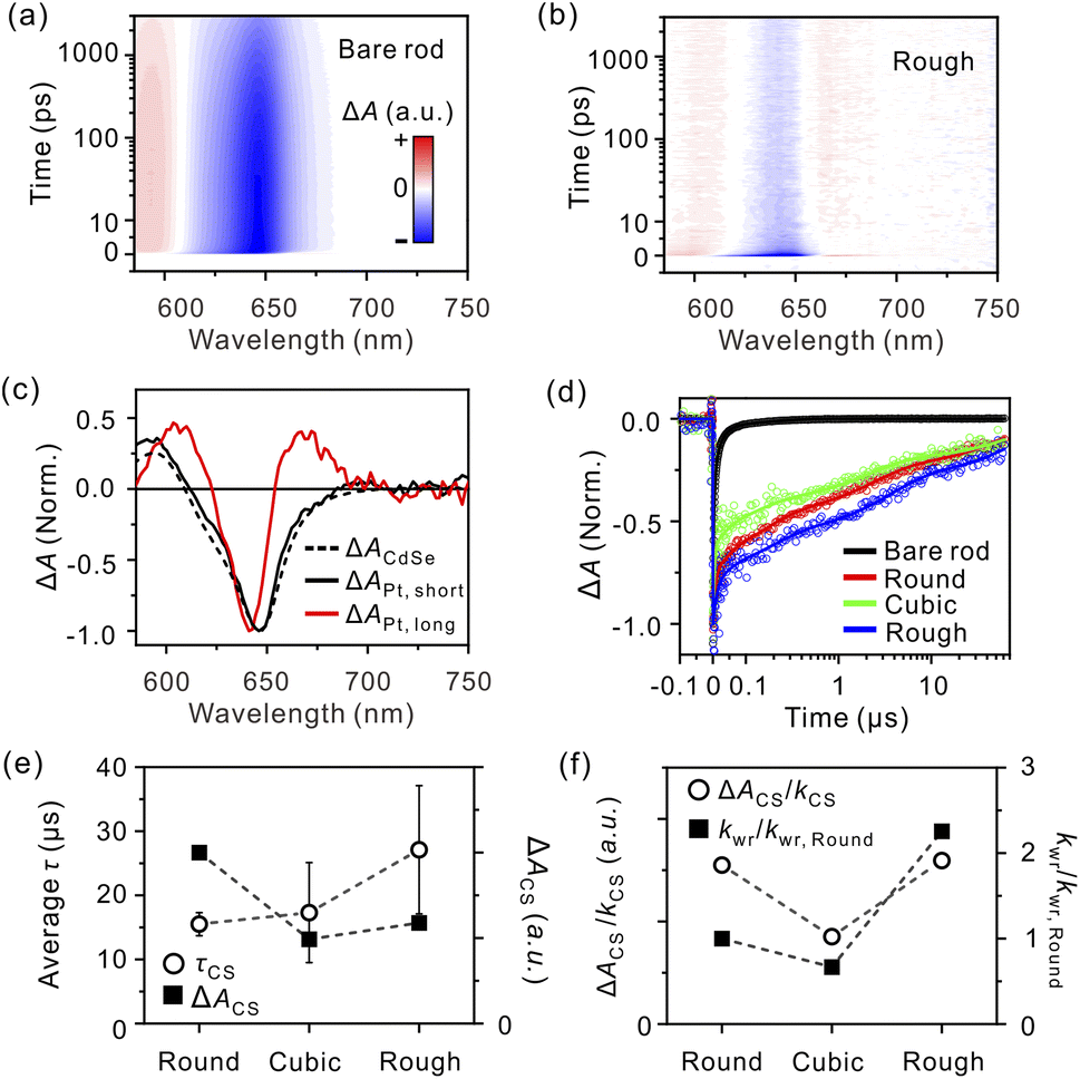 | ||
| Fig. 3 Femtosecond-resolved TA maps of (a) bare nanorods and (b) Rough upon excitation at 550 nm. All TA spectra were collected under single excitonic conditions; see Fig. S9, ESI.† (c) Spectra of short-lived (black, solid line) and long-lived (red, solid line) global-lifetime components of Rough. The TA spectrum originating from the excitons of CdSe (black, dashed line) is presented for comparison; see ESI.† (d) Nanosecond-resolved bleaching–recovery profiles monitored at 645 nm. (e) Observed lifetimes (τCS, circles) and amplitudes (ΔACS, squares) of the CS state depending on the morphology of the metal tip. (f) Carrier dynamics (ΔACS/kCS, circles) and relative surface reaction rates (kwr/kwr,Round, squares) depending on the morphology of the metal tip. | ||
To relate the time-dependent spectral change to the charge transfer and recombination dynamics, we constructed lifetime-associated spectra over the entire spectral and temporal ranges by global-lifetime analysis (see Global-lifetime analysis, ESI†).34 This analysis is useful for distinguishing the absorption spectrum of charge carriers in the CdSe domain from that of the CS state. When both an electron and a hole reside in the CdSe domain, the spectrum is manifested by the XB band centered at ∼645 nm and the positive PIA band at around 600 nm (Fig. 3c, black, dashed line). The lifetime-associated spectra of the short-lived components for Rough (Fig. 3c, black, solid line, and Fig. S12, ESI†) match the TA spectrum of excitons in the bare rods, showing that the exciton dissociates into charge carriers and the electron transfers to the metal tips immediately after the photoexcitation. After these processes, only a hole resides in the CdSe domains, producing a long-lived, peak–dip–peak-shape TA spectral feature (Fig. 3c, red, solid line); regardless of the counterpart of the electron transfer, the peak–dip–peak feature has been commonly observed in the literature, and we attribute the symmetric shape to the characteristics of the hole in the CdSe domain.32 The nanosecond-resolved lifetime-associated spectra of the tipped rods with the same symmetric shapes indicate that all components survive on the ns-to-μs timescales originating from the CS state (Fig. S12e, ESI†). It follows that the ΔA of the slowest component analyzed from the femtosecond-resolved TA spectra is a measure of the CS state amount for each sample (Fig. S13, ESI†). Accordingly, we deduce the lifetime of the CS state from the nanosecond-resolved TA trajectory. The overall lifetimes of the CS states (τCS) are obtained by amplitude-weighted averaging of lifetime, as 15.5 ± 1.8, 17.3 ± 7.8, and 27.1 ± 10.0 μs for Round, Cubic, and Rough, respectively (Table S3, ESI†). Fig. 3e summarizes the lifetime and initial amount of the long-lived CS states for each morphology. The amount of charge carriers at the Pt tips, proportional to the extent of the CS state formation, ΔACS, is the largest for Round compared to Cubic and Rough. The lifetime of the CS state is similar for Round and Cubic but reaches the maximum for Rough.
The water reduction has been reported to occur on the millisecond timescale,35 far slower than the relaxation of the CS state. Under this condition (kCS ≫ kwr), eqn (1) can be simplified as follows:
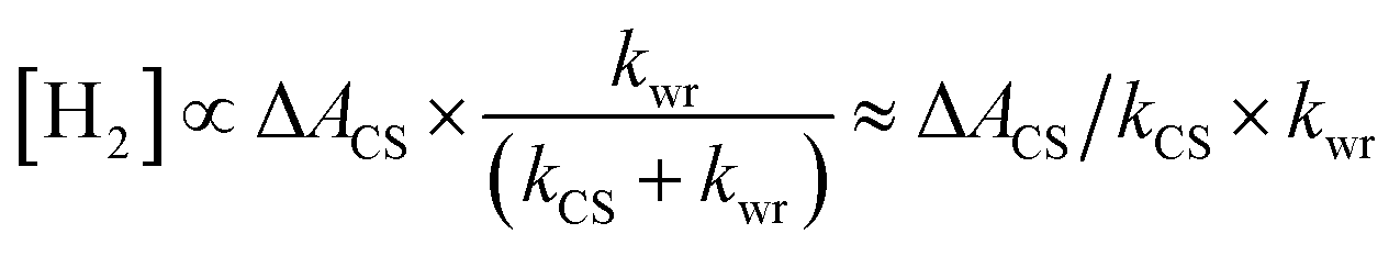 | (2) |
The term ΔACS/kCS relates to the carrier dynamics within the Pt–CdSe nanorods and represents the value of charge carriers on the Pt tips feasible for reacting with water, and kwr is the surface reaction rate on the Pt tips.
To stringently compare the effect of morphology and surface structure of the Pt cocatalyst on carrier dynamics, we kept the elemental ratio of Pt to CdSe constant, thus minimizing the size effect of the Pt tips across all samples. For cubic tips, most surface atoms lie on the clean {100} facets with fewer corners and edge sites.25 It is known that the Fermi level of Pt{100} facets is higher than that of Pt{111}.24 It follows that the CS states in Cubic are the least favorable among the Pt morphologies; the measure of ΔACS/kCS is distinctively low for Cubic but nearly identical for Round and Rough (Fig. 3f, circles). Rough tips host a significant fraction of surface defects, and round tips are also composed of multiple poly-oriented facets with many edges at the boundaries,22 which trap electrons and increase the CS state lifetime.
Because we compare the relative extents of the CS state (ΔACS) formation through the TA measurements, we only estimate the ratio of kwr among the Pt–CdSe nanorods from eqn (2) using the extracted rate constants and observed hydrogen-evolution rates. Assuming that the water reduction with Round occurs on a millisecond scale, we deduce the relative ratio of kwr, 1![[thin space (1/6-em)]](https://www.rsc.org/images/entities/char_2009.gif) :0.67:2.2 for Round:Cubic:Rough (Fig. 3f, squares).35
:0.67:2.2 for Round:Cubic:Rough (Fig. 3f, squares).35
The electrochemically active surface area (ECSA) for the catalysts was estimated to be 132.5 cm2 mg−1 for Round, 159.6 cm2 mg−1 for Cubic, and 141.6 cm2 mg−1 for Rough (Fig. S14, ESI†),36 revealing that the surface area of the Pt tips is not the primary factor of the large surface activity differences. Instead, there is a consensus about the correlation of catalytic performances with the surface sites in heterogeneous reactions. In photocatalytic hydrogen evolution, it was reported that the water adsorption energy on Pt(100) facets was lower than that on Pt(111),37 which was suggested as a descriptor for the activity difference. For Cubic, the surface facets are dominantly Pt(100) with uniform orientations (Fig. 1b). For Round, the lattice fringe is assigned to Pt(111), and the surface facets are analyzed as a mixture of (100) and (111) with different orientations surrounding the round morphology (Fig. 1a). These structural features elucidate the low activity of Cubic compared to other morphologies.24,25,37 For Rough, the Pt tips show irregular morphology (Fig. 1c). The surface analysis in the HRTEM images shows that a significant fraction of the surface faces is composed of (311). By the fast Fourier transform (FFT) of the HRTEM image, the (311) pattern is identified with the intense (100) and (111) patterns along the [011] zone axis (Fig. S15, ESI†). The theoretical calculation and reaction study revealed that the low coordination sites of the Pt surface distinctively stabilized the intermediate states, such as surface-adsorbed hydrogen atoms, and eventually lowered the activation energy of hydrogen evolution reactions.38–42 Accordingly, the high-energy surfaces with multiple edges and undercoordinated sites of Rough significantly promoted the surface reaction and presented the maximum kwr.
Conclusions
In conclusion, the impact of cocatalyst morphology on the photocatalytic activity of semiconductor nanorod catalysts was systematically investigated. Three distinct morphologies of Pt tips, Round, Cubic, and Rough, were prepared for hydrogen evolution reactions. The results reveal a significant difference in hydrogen evolution rates, with Rough exhibiting six times higher activity than Cubic. Detailed kinetic analysis shows that Cubic hosts fewer short-lived CS states and exhibits less surface activity. In contrast, Rough has a similar value of CS state feasible for reacting with water but much higher surface activity than Round, resulting in the maximum hydrogen evolution rate. These findings demonstrate that engineering the cocatalyst morphology, in addition to composition and size, is critical for optimizing photochemical activity. We suggest that rational treatment of metal deposition on conventional photocatalysts can significantly enhance catalytic activity.Data availability
All experimental and characterization data are available in the ESI.†Author contributions
B. P., O.-H. K. and H. S. designed the experiments. B. P. and J. C. prepared the catalysts and measured photocatalytic properties. W. C. measured electrochemical surface area. W.-W. P., Y. M. S. and S. S. performed time-resolved spectroscopy measurements. All authors analyzed the experimental results and wrote the manuscript.Conflicts of interest
There are no conflicts of interest to declare.Acknowledgements
This work was supported by the National Research Foundation (NRF), funded by the Ministry of Science and ICT, Republic of Korea (2018R1A5A1025208, RS-2023-00208239, 2020R1A2C1014203, and 2022R1A4A1033247). O.-H. K. and W.-W. P. are grateful for the support from SAIT's Global Research Outreach (GRO) Program.Notes and references
- R. J. Detz, J. N. H. Reek and B. C. C. van der Zwaan, Energy Environ. Sci., 2018, 11, 1653–1669 RSC.
- N. S. Lewis and D. G. Nocera, Proc. Natl. Acad. Sci. U. S. A., 2006, 103, 15729–15735 CrossRef CAS PubMed.
- A. Kudo and Y. Miseki, Chem. Soc. Rev., 2009, 38, 253–278 RSC.
- A. Fujishima and K. Honda, Nature, 1972, 238, 37–38 CrossRef CAS PubMed.
- U. Banin, Y. Ben-Shahar and K. Vinokurov, Chem. Mater., 2014, 26, 97–110 CrossRef CAS.
- P. Kalisman, Y. Nakibli and L. Amirav, Nano Lett., 2016, 16, 1776–1781 CrossRef CAS PubMed.
- J. Y. Choi, W.-W. Park, B. Park, S. Sul, O.-H. Kwon and H. Song, ACS Catal., 2021, 11, 13303–13311 CrossRef CAS.
- J. U. Bang, S. J. Lee, J. S. Jang, W. Choi and H. Song, J. Phys. Chem. Lett., 2012, 3, 3781–3785 CrossRef CAS PubMed.
- J. Y. Choi, K. M. Nam and H. Song, J. Mater. Chem. A, 2018, 6, 16316–16321 RSC.
- J. Y. Choi, D. Jeong, S. J. Lee, D.-G. Kang, S. K. Kim, K. M. Nam and H. Song, Nano Lett., 2017, 17, 5688–5694 CrossRef CAS PubMed.
- P. Kalisman, L. Houben, E. Aronovitch, Y. Kauffmann, M. Bar-Sadan and L. Amirav, J. Mater. Chem. A, 2015, 3, 19679–19682 RSC.
- Y. Liu, W. Yang, Q. Chen, D. A. Cullen, Z. Xie and T. Lian, J. Am. Chem. Soc., 2022, 144, 2705–2715 CrossRef CAS PubMed.
- F. Calle-Vallejo, J. Tymoczko, V. Colic, Q. H. Vu, M. D. Pohl, K. Morgenstern, D. Loffreda, P. Sautet, W. Schuhmann and A. S. Bandarenka, Science, 2015, 350, 185–189 CrossRef CAS PubMed.
- J. Xiao, J. J. M. Vequizo, T. Hisatomi, J. Rabeah, M. Nakabayashi, Z. Wang, Q. Xiao, H. Li, Z. Pan, M. Krause, N. Yin, G. Smith, N. Shibata, A. Brückner, A. Yamakata, T. Takata and K. Domen, J. Am. Chem. Soc., 2021, 143, 10059–10064 CrossRef CAS PubMed.
- J. Liu, Z. Wei and W. Shangguan, ChemCatChem, 2019, 11, 6177–6189 CrossRef CAS.
- S. E. Habas, P. Yang and T. Mokari, J. Am. Chem. Soc., 2008, 130, 3294–3295 CrossRef CAS PubMed.
- H. Schlicke, D. Ghosh, L.-K. Fong, H. L. Xin, H. Zheng and A. P. Alivisatos, Angew. Chem., Int. Ed., 2013, 52, 980–982 CrossRef CAS PubMed.
- S. Cheong, J. D. Watt and R. D. Tilley, Nanoscale, 2010, 2, 2045–2053 RSC.
- X. Teng, X. Liang, S. Maksimuk and H. Yang, Small, 2006, 2, 249–253 CrossRef CAS PubMed.
- E. Khon, A. Mereshchenko, A. N. Tarnovsky, K. Acharya, A. Klinkova, N. N. Hewa-Kasakarage, I. Nemitz and M. Zamkov, Nano Lett., 2011, 11, 1792–1799 CrossRef CAS PubMed.
- M. Wang, S. Shen, L. Li, Z. Tang and J. Yang, J. Mater. Sci., 2017, 52, 5155–5164 CrossRef CAS.
- M. J. Hossain, M. M. Rahman and Md. H. Sharif, Nanoscale Adv., 2020, 2, 1245–1252 RSC.
- B. M. Amoli, S. Gumfekar, A. Hu, Y. N. Zhou and B. Zhao, J. Mater. Chem., 2012, 22, 20048–20056 RSC.
- E. Cui and G. Lu, J. Phys. Chem. C, 2013, 117, 26415–26425 CrossRef CAS.
- S. Cao, J. Jiang, B. Zhu and J. Yu, Phys. Chem. Chem. Phys., 2016, 18, 19457–19463 RSC.
- M. Luo, W. Yao, C. Huang, Q. Wu and Q. Xu, J. Mater. Chem. A, 2015, 3, 13884–13891 RSC.
- M. Luo, P. Lu, W. Yao, C. Huang, Q. Xu, Q. Wu, Y. Kuwahara and H. Yamashita, ACS Appl. Mater. Interfaces, 2016, 8, 20667–20674 CrossRef CAS PubMed.
- J. Yao, Y. Jheng, X. Jia, L. Duan, Q. Wu, C. Huang, W. An, Q. Xu and W. Yao, ACS Appl. Mater. Interfaces, 2019, 11, 25844–25853 CrossRef CAS PubMed.
- K. Wu, Z. Chen, H. Lv, H. Zhu, C. L. Hill and T. Lian, J. Am. Chem. Soc., 2014, 136, 7708–7716 CrossRef CAS PubMed.
- P. Yu, X. Wen, Y.-C. Lee, W.-C. Lee, C.-C. Kang and J. Tang, J. Phys. Chem. Lett., 2013, 4, 3596–3601 CrossRef CAS.
- Z.-J. Jiang and D. F. Kelley, J. Phys. Chem. C, 2011, 115, 4594–4602 CrossRef CAS.
- K. Wu, Q. Li, Y. Du, Z. Chen and T. Lian, Chem. Sci., 2015, 6, 1049–1054 RSC.
- V. I. Klimov and D. W. McBranch, Phys. Rev. Lett., 1998, 80, 4028–4031 CrossRef CAS.
- H.-W. Nho, W.-W. Park, B. Lee, S. Kim, C. Yang and O.-H. Kwon, Phys. Chem. Chem. Phys., 2022, 24, 1982–1992 RSC.
- T. Chen, Z. Feng, G. Wu, J. Shi, G. Ma, P. Ying and C. Li, J. Phys. Chem. C, 2007, 111, 8005–8014 CrossRef CAS.
- M. Shao, J. H. Odell, S.-I. Choi and Y. Xia, Electrochem. Commun., 2013, 31, 46–48 CrossRef CAS.
- M. Wang, H. Liu, J. Ma and G. Lu, Appl. Catal., B, 2020, 266, 118647 CrossRef CAS.
- Y. Jang, K.-H. Choi, D. Y. Chung, J. E. Lee, N. Jung and Y.-E. Sung, ChemSusChem, 2017, 10, 3063–3068 CrossRef CAS PubMed.
- M. A. Mahmoud, C. E. Tabor, M. A. El-Sayed, Y. Ding and Z. L. Wang, J. Am. Chem. Soc., 2008, 130, 4590–4591 CrossRef CAS PubMed.
- G. J. Leong, M. C. Schulze, M. B. Strand, D. Maloney, S. L. Frisco, H. N. Dinh, B. Pivovar and R. M. Richards, Appl. Organomet. Chem., 2014, 28, 1–17 CrossRef CAS.
- R. Kajiwara, Y. Asaumi, M. Nakamura and N. Hoshi, J. Electroanal. Chem., 2011, 657, 61–65 CrossRef CAS.
- X. Bao, Y. Gong, X. Zheng, J. Chen, S. Mao and Y. Wang, J. Energy Chem., 2020, 51, 272–279 CrossRef.
Footnotes |
| † Electronic supplementary information (ESI) available. See DOI: https://doi.org/10.1039/d3sc01429k |
| ‡ These authors contributed equally to this work. |
| § Present address: Department of Chemistry, University of Colorado Boulder, Boulder, Colorado 80309, United States. |
| ¶ Present address: Lawrence Berkeley Laboratory, 1 Cyclotron Road, Berkeley, CA 94720, United States. |
| This journal is © The Royal Society of Chemistry 2023 |