
 Open Access Article
 This Open Access Article is licensed under a Creative Commons Attribution-Non Commercial 3.0 Unported Licence
Photogenerated charge transfer in Dion–Jacobson type layered perovskite based on naphthalene diimide†
Simon
Nussbaum
 a,
Etienne
Socie
b,
George C.
Fish
b,
Nicolas J.
Diercks
a,
Hannes
Hempel
c,
Dennis
Friedrich
d,
Jacques-E.
Moser
b,
Jun-Ho
Yum
*a and
Kevin
Sivula
*a
a,
Etienne
Socie
b,
George C.
Fish
b,
Nicolas J.
Diercks
a,
Hannes
Hempel
c,
Dennis
Friedrich
d,
Jacques-E.
Moser
b,
Jun-Ho
Yum
*a and
Kevin
Sivula
*a
aLaboratory for Molecular Engineering of Optoelectronic Nanomaterials, Institute of Chemical Sciences and Engineering (ISIC), École Polytechnique Fédérale de Lausanne (EPFL), 1015 Lausanne, Switzerland. E-mail: junho.yum@epfl.ch; kevin.sivula@epfl.ch
bPhotochemical Dynamics Group, Institute of Chemical Sciences and Engineering (ISIC), École Polytechnique Fédérale de Lausanne (EPFL), 1015 Lausanne, Switzerland
cDepartment of Structure and Dynamics of Energy Materials, Helmholtz Zentrum Berlin für Materialien und Energie, Hahn-Meitner-Platz 1, 140109 Berlin, Germany
dInstitute for Solar Fuels, Helmholtz Zentrum Berlin für Materialien und Energie, Hahn-Meitner-Platz 1, 140109 Berlin, Germany
First published on 15th May 2023
Abstract
Incorporating organic semiconducting spacer cations into layered lead halide perovskite structures provides a powerful approach to mitigate the typical strong dielectric and quantum confinement effects by inducing charge-transfer between the organic and inorganic layers. Herein we report the synthesis and characterization of thin films of novel DJ-phase organic–inorganic layered perovskite semiconductors using a naphthalene diimide (NDI) based divalent spacer cation, which is shown to accept photogenerated electrons from the inorganic layer. With alkyl chain lengths of 6 carbons, an NDI-based thin film exhibited electron mobility (based on space charge-limited current for quasi-layered 〈n〉 = 5 material) was found to be as high as 0.03 cm2 V−1 s−1 with no observable trap-filling region suggesting trap passivation by the NDI spacer cation.
Introduction
Layered hybrid organic–inorganic perovskites (LHOIPs) are a novel class of semiconductors that can be formed by replacing the A-site in a conventional (ABX3) perovskite with a bulky organic spacer cation such as butylammonium (BA) or phenylethyl-ammonium (PEA) forming a Ruddlesden–Popper (RP)-type crystalline structure of alternating organic and inorganic layers.1,2 Lead halide LHOIPs based on mono-cations like PEA and BA have been intensively studied for optoelectronic applications. The incorporation of organic spacer di-cations forming what is commonly called a quasi-Dion–Jacobson (DJ)-type LHOIP with a general formula of (BOS)(A)n−1PbnI3n+1, where BOS represents a bulky organic spacer di-cation and A is a small monovalent cation (e.g. methylammonium, MA), have recently come forward as more promising materials due to enhanced stability and improved charge carrier transport through the organic layer.3–7 A powerful and promising approach to further tune the optoelectronic properties of these materials is by incorporating π–π conjugated semiconducting BOSs into the layered perovskite structure.8–10 This has been demonstrated to facilitate inter-layer charge carrier mobility11 and the formation of long-lived charge-transfer excitons by spatially separating electrons and holes in different layers.12–14 Moreover, given the facile preparation of these materials by scalable solution-based techniques, they have great potential in next-generation, inexpensive, and high-performance solar cells,15 light-emitting diodes,16,17 and other optoelectronic devices.18Incorporating semiconducting BOSs, however, remains challenging due to their relatively large size and strong intra-molecular interactions which hamper the self-assembly of the layered crystalline structure from solution-based processes. A promising electron-accepting organic chromophore building block is naphthalene diimide (NDI), which has been used extensively in conjugated polymers.19,20 Indeed, electron transfer from lead iodide nanowires to an NDI chromophore has been reported previously,21–23 and monovalent spacer cations based on NDI have been incorporated into Ruddlesden–Popper (RP) phase layered perovskite structures.24 However, the successful synthesis of an NDI-containing DJ-phase LHIOP has remained elusive. Previous research on divalent NDI-cations with short amine-bearing alkane chains (coded as NDIC2, structure displayed in Fig. 1a) reported the formation of one-dimensional (1D) perovskitoid structures rather than two-dimensional (2D) layered materials and its application in optoelectronic devices was limited due to the structural disorder of the material.25,26 Herein we show that the formation of (quasi-2D) LHOIPs can be obtained when using a divalent NDI-based chromophore, which leads to formation of the type II nano-heterostructure. This leads to the first demonstration of photogenerated charge transfer in NDI-based DJ-type LHOIPs and characterization of the electronic properties of subsequent quasi LHOIPs by space charge limited current (SCLC) measurements and transient absorption spectroscopy.
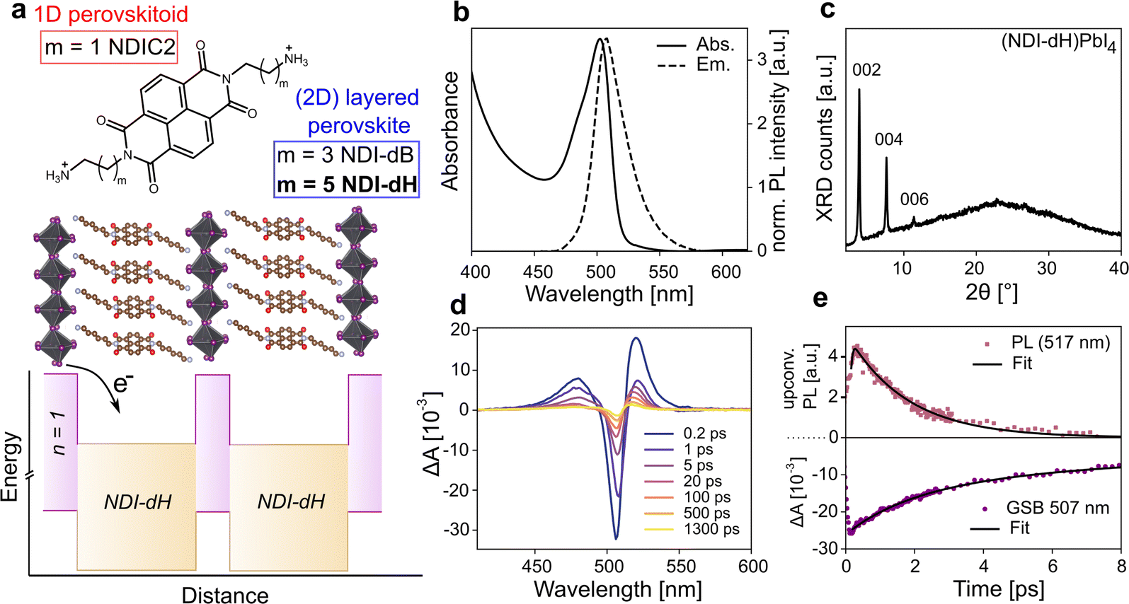 | ||
| Fig. 1 (a) Chemical structure of the herein investigated divalent spacer cations and aimed layered structure shown with various sub-band well width of the inorganic layer. (b) UV-vis and PL steady-state spectra and (c) XRD of the (NDI-dH)PbI4. XRD was recorded with a monochromated Cu Kα1 X-ray source (d) transient absorption spectral slices, and (e) ultrafast PL and GSB dynamics of the (NDI-dH)PbI4 films based on fluorescence upconversion spectroscopy (FLUPS) and TA, respectively. | ||
Results and discussion
Formation of NDI-based DJ-type LJOIPs
We prepared NDI-based di-cations with different alkyl chain lengths of 4 or 6 carbons coded as NDI-dB and NDI-dH, respectively. The chemical structures of the spacer cations are shown in Fig. 1a. Detailed synthesis procedures (Scheme S1, and S2†), characterization, and the LHOIP thin film fabrication with these cations are provided in the ESI.† Starting with the (NDI-dH)PbI4 composition (n = 1), the visible light absorption and photoluminescence (PL) spectra of the synthesized thin films are displayed in Fig. 1b and show the typical excitonic absorption and emission bands similarly found in conventional (PEA)2PbI4 and (BA)2PbI4 layered perovskites.27 However, in contrast to (BA)2PbI4, the photoluminescence intensity is significantly quenched in the NDI-based films as displayed in Fig. S1.†Fig. 1c displays the XRD pattern of the thin film showing equally spaced diffraction peaks associated with the 00![[small script l]](https://www.rsc.org/images/entities/i_char_e146.gif) -planes suggesting the successful formation of a layered perovskite crystal phase where the inorganic slabs are oriented parallel to the substrate. Based on an assignment of the peak at 2θ = 3.84°, the inter-layer spacing is 22.9 Å corresponding roughly to the size expected given the length of the NDI-dH cation of 22.7 Å. We note that the optoelectronic and structural properties of our (NDI-dH)PbI4 thin films are distinct from the previously reported 1D perovskitoid films based on the similar spacer cation with an ethyl-ammonium linker (NDIC2) where no excitonic absorption and emission bands were found.25,26 Notably, the desired DJ-type layered structure can also be obtained with the butylammonium linker (NDI-dB). Similar optoelectronic properties with quenched photoluminescence and XRD diffraction peaks associated with a smaller inter-layer distance of 19.3 Å are observed (Fig. S1 and S2†). The observed effects of the alkane linker chain on structure and crystallinity are consistent with our previous finding in RP-based perovskite indicating that the amine-bearing alkane chain linker is an important parameter in the formation of layered perovskite materials.24
-planes suggesting the successful formation of a layered perovskite crystal phase where the inorganic slabs are oriented parallel to the substrate. Based on an assignment of the peak at 2θ = 3.84°, the inter-layer spacing is 22.9 Å corresponding roughly to the size expected given the length of the NDI-dH cation of 22.7 Å. We note that the optoelectronic and structural properties of our (NDI-dH)PbI4 thin films are distinct from the previously reported 1D perovskitoid films based on the similar spacer cation with an ethyl-ammonium linker (NDIC2) where no excitonic absorption and emission bands were found.25,26 Notably, the desired DJ-type layered structure can also be obtained with the butylammonium linker (NDI-dB). Similar optoelectronic properties with quenched photoluminescence and XRD diffraction peaks associated with a smaller inter-layer distance of 19.3 Å are observed (Fig. S1 and S2†). The observed effects of the alkane linker chain on structure and crystallinity are consistent with our previous finding in RP-based perovskite indicating that the amine-bearing alkane chain linker is an important parameter in the formation of layered perovskite materials.24
Charge dynamics in NDI-based DJ-type LJOIPs
To further investigate the effect of the NDI-spacer cation on the photogenerated charge carrier dynamics, ultrafast spectroscopic techniques were performed, namely transient absorption (TA) spectroscopy and ultrafast broadband fluorescence upconversion spectroscopy (FLUPS).28,29 Due to the improved solution-processed thin-film morphology of the layered perovskite prepared with NDI-dH compared to the NDI-dB cation (Fig. S3†), which is likely due to a difference in cation solubility, we focus on the NDI-dH divalent spacer cation system in the following analysis.The TA and FLUPS spectra and dynamics are shown in Fig. 1d, e and S4† for (NDI-dH)PbI4. The FLUPS spectrum shows an ultrashort photoluminescence (PL) lifetime with a decay time constant of around 1.65 ± 0.03 ps, which is comparable to the previously reported PL decay with RP-type analog materials, and can be attributed to electron transfer from the inorganic layer to the organic spacer as schematically illustrated in Fig. 1a.24
The ultrafast PL decay stands in contrast to reported (PEA)2PbI4 where decay times of several hundreds of picoseconds are reported.30 The TA spectra show a ground state bleaching (GSB) at 507 nm corresponding to the position of the excitonic absorption band. The weak spectral signature of the expected NDI− formation overlaps with the photoinduced absorption (PIA) at 450–550 nm.25,26 However, we note that the partial GSB decay and complete PL decay are characteristic of electron transfer processes.31
GSB dynamics were fit to a tri-exponential decay resulting in one fast decay constant (τ1 = 1.66 ps) followed by two slower decays with τ2 = 6.11 ps and τ3 = 1510 ps. Altering the pulsed laser fluence from 15 to 150 nJ showed no change in the TA spectra suggesting that Auger-type recombination processes do not contribute to the GSB dynamics (Fig. S4†). While τ1 can be attributed to the electron transfer from the inorganic layer to the NDI spacer due to the similar time scale as the observed PL decay, the long decay components (τ2 and τ3) are attributed to potential electron back transfer from the NDI to the perovskite ground state and non-radiative recombination.
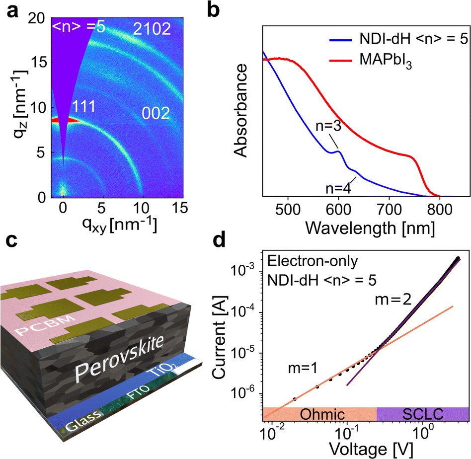
To investigate further the nature of the charge-separation state at the organic–inorganic nano-interface, flash photolysis time-resolved microwave conductivity (fp-TRMC) measurements were performed. Probing the photogenerated charge carriers along the direction parallel to the substrate (displayed schematically in Fig. 2a) by exciting the LHOIP at 420 nm, the microwave probe is only absorbed by free charge carriers allowing assessment of the sum of their mobilities, μ, and the obtained free charge carrier generation yield (φ) by the formula:32
 | ||
| Fig. 2 (a) Illustration of the fp-TRMC setup measuring the mobilities of free charge carriers along the axis parallel to the substrate and (b) fp-TRMC transient of (NDI-dH)PbI4 (black closed circles) and (BA)2PbI4 (red closed circles) with the obtained mobilities in the inset figure. Samples were excited at 420 nm. | ||
Moreover, the estimated mobility, as quantified by the sum mobility (φΣμ) in (NDI-dH)PbI4 is around one order of magnitude higher than previously reported in NDIC2-based 1D perovskitoid materials.21,25 This increased sum mobility can be attributed to the 2D layered structure. However, the results are still more than one order of magnitude lower than the BA-based perovskite reference material. Although it is possible that the free charge carrier generation yield (φ) is lower for (NDI-dH)PbI4 resulting in decreased apparent mobilities from the fp-TRMC data, we suppose that the diminished sum mobility (φΣμ) observed for (NDI-dH)PbI4 is due to the decreased sum mobility of the electrons located in the NDI layer. As the minimum time-resolution of fp-TRMC (few ns) is larger than the time scale of electron transfer from the inorganic layer to the NDI chromophore, optical pump-terahertz probe (OPTP) spectroscopy was used to determine the sum mobilities, a few picoseconds after excitation at 400 nm. The transient intrinsic carrier sum mobility dynamics derived from the transient THz spectroscopy signal is displayed in Fig. S6† and shows a biexponential decay with time constants of τ1 = 0.55 ps and τ2 ≈ 15 ps (Table S1†). Given the similarities in time scale observed in FLUPS for the electron transfer, we assign the faster decay component to be the formation of charge-transfer excitons (CTE) overlapping with contributions due to electron–phonon scattering. The obtained peak sum mobility determined by OPTP was found to be 0.35 cm2 V−1 s−1 which is in the same range as previously reported mobilities for BA-based and PEA-based perovskites further suggesting that φ can be assumed to be similar in (NDI-dH)PbI4 and (BA)2PbI4.34,35
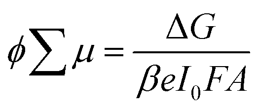
Given the successful formation of the ordered and crystalline layered (NDI-dH)PbI4 perovskite phase, we investigated whether a quasi-2D layered structure is preserved when the energy sub-band width is increased. Thin films with larger quantum well width and higher n-number (as shown schematically in Fig. 3a) were fabricated by mixing an appropriate amount of methylammonium iodine (MA) into the precursor solution. In the following, the stoichiometric ratio in the precursor solution will be denoted by the indices 〈n〉 indicating the nominal quantum well width of (NDI-dH)MAn-1PbnI3n+1 expected to be formed. For films with 〈n〉 > 1, a distribution of quantum wells of various well widths is usually formed.36 For the sake of clarity, the specific perovskite layer number phase will be denoted by the indices n. The visible light absorbance and XRD spectra of thin films with 〈n〉 = 2 or 3 are displayed in Fig. 3b and S7.† For 〈n〉 = 2 the formation n = 2, 3 phases can be observed as indicated by the characteristic excitonic absorption bands with an absorption maximum at 560 nm and 600 nm, respectively. Electron transfer kinetics were further investigated by analysis of the GSB-dynamics from TA spectroscopy (Fig. 3c).
 | ||
| Fig. 3 (a) Illustration of the electronic structure for NDI-based quasi LHOIP materials. CB and VB energy levels were derived from BA-based perovskites as previous reported in ref. 36 (b) UV-vis absorption spectra of (NDI-dH)-based perovskite films with 〈n〉 = 1, 2, 3 and (c) transient absorption spectral slices of 〈n〉 = 3 thin film. | ||
A strong GSB bleach for the n = 2 and n = 3 phases can be observed. The 0.25 ps growth component of the GSB in the n = 3 phase is attributed to the electron funneling as reported for similar systems.38,39 Notably in the 〈n〉 = 3 film, a weak feature in the range of 450 to 500 nm with a delay of around 1 ps can be observed potentially arising from the NDI− anion. However, the signal was too weak to further resolve. The dynamics of the GSB decay were fitted to a tri-exponential decay (Fig. S8†). The decay components and fitting results (Table S2†) are consistent with an ultrafast decay component τ1 attributed to the electron transfer from the inorganic layer to the NDI since a clear trend of increasing GSB decay time with an increase in the well width (n) is found. The attribution of τ1 to the electron transfer from the inorganic layer to the NDI chromophore has been proposed by Proppe et al., in 1D perovskitoid materials incorporating NDI-C2.26 The increase in the GSB decay time (τ1) is plausibly ascribed to the decreased conduction band energy of the perovskite, which reduces the driving force for electron transfer and reduces quantum confinement as the quantum well width increases, requiring longer time for photogenerated carriers to diffuse to the NDI chromophore. For films with 〈n〉 = 4 and 5, the visible light absorption (Fig. S9†) does not show any excitonic absorption bands that can be assigned to the n = 2, 3 phases suggesting suppression of the formation of lower n-phases. These findings were further supported by the TA where, for the films 〈n〉 = 4–5, only one single ground state bleaching can be observed. The GSB minima shift towards lower absorption energies with increasing 〈n〉 (Fig. S10†) and can be associated with quasi-layered perovskite phases with large inorganic well-width. GSB decay dynamics are displayed in Fig. S11† and show comparable dynamics compared to lower n-phases. Notably, τ1 attributed to the electron transfer is similar for 〈n〉 = 4 and 〈n〉 = 5 films while the exact decay may be distorted by potential electron funneling processes resulting in faster initial GSB decay in 〈n〉 = 5 compared to 〈n〉 = 4.
Electronic properties of NDI-based DJ-type LJOIPs
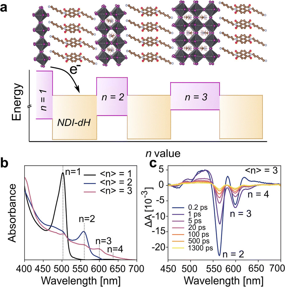
Given the spectroscopic results, which show that photons absorbed by the perovskite layers lead to free electrons in the NDI layers, we next aimed to obtain device-based electronic characterization to demonstrate that the quasi-2D layered structure has suitable charge carrier transport properties. We focused on 〈n〉 = 5 films as similar perovskite structures based on butylammonium (BA) have been reported,37 allowing us to compare our new material with the established system. The crystallinity and orientation of the (NDI-dH)(MA)4Pb5I16 thin films were optimized based on a solvent engineering method.In brief, we found that a solvent mixture of dimethylformamide (DMF):dimethyl sulfoxide (DMSO) (2![[thin space (1/6-em)]](https://www.rsc.org/images/entities/char_2009.gif) :3 v/v) in the precursor solution results in thin films where the inorganic layers are oriented perpendicular to the substrate as shown by gracing-incident wide angle X-ray scattering (GIWAXS) in Fig. 4a and XRD (Fig. S12†). Visible light absorbance (Fig. 4b) of the films prepared under these conditions show excitonic absorption bands which can be assigned to n = 3 and 4 phases. Comparing the absorption spectrum of the optimized 〈n〉 = 5 films with the absorption spectrum of MAPbI3 indicates no obvious formation of the 3D perovskite phase. We were unable to obtain any PL signal for the 〈n〉 = 5 films (Fig. S13†) likely due to electron transfer from the inorganic wells to the NDI spacer chromophore.
:3 v/v) in the precursor solution results in thin films where the inorganic layers are oriented perpendicular to the substrate as shown by gracing-incident wide angle X-ray scattering (GIWAXS) in Fig. 4a and XRD (Fig. S12†). Visible light absorbance (Fig. 4b) of the films prepared under these conditions show excitonic absorption bands which can be assigned to n = 3 and 4 phases. Comparing the absorption spectrum of the optimized 〈n〉 = 5 films with the absorption spectrum of MAPbI3 indicates no obvious formation of the 3D perovskite phase. We were unable to obtain any PL signal for the 〈n〉 = 5 films (Fig. S13†) likely due to electron transfer from the inorganic wells to the NDI spacer chromophore.
 | ||
| Fig. 4 (a) GIWAXS of optimized 〈n〉 = 5 NDI-dH based perovskite thin film and (b) resulting UV-vis absorbance spectra. (c) shows the architecture for electron-only SCLC measurements and (d) the resulting SCLC I–V curve obtained with this architecture. | ||
Based on thin films prepared with these optimized conditions, the electron mobility in the direction perpendicular to the substrate was obtained using widely reported device architecture where the perovskite layer is sandwiched between two electron-transport layers (TiO2 and PCBM) as illustrated in Fig. 4c. Different perovskite layer thicknesses ranging from 600 nm to 1.2 μm, as displayed in the cross-section electron micrographs (Fig. S14†), were fabricated. A typical current–voltage (I–V) curve of the electron-only space charge-limited current (SCLC) is displayed in Fig. 4d. At low voltage, a linear dependence between the current and voltage can be found marking an ohmic region. At higher voltage, a transition towards an I ∝ V2 region is observed, indicating SCLC behavior.
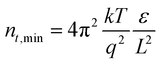
The absence of any region with I ∝ Vm where m > 3, corresponding to a trap-filling region (TFR), is surprising as TFRs are routinely reported in BA-based perovskite films. Indeed, such an I–V-curve with a clear trap-filling region was observed when (BA)2(MA)4Pb5I16 (〈n〉 = 5) films were investigated using the same device architecture (Fig. S15†). It is thus assumed that the trap density in the NDI-dH based film is below the minimal trap density (nt_min = 6 × 10⁻¹⁴ cm−3 at T = 295 K and L = 1.2 μm) for the investigated thickness (L), as given by:40
where ε is the relative permittivity of the material, ε0 is the vacuum permittivity, V is the applied voltage, and L is the thickness of the perovskite layer. The relative permittivity for the NDI 〈n〉 = 5 was estimated to be ε0 = 16 based on the capacitance determined by impedance spectroscopy (Fig. S16†).
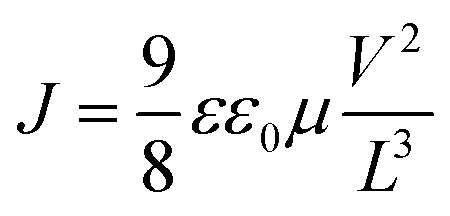
Electron mobility of 0.03 cm2 V−1 s−1 was found for the (NDI-dH)(MA)4Pb5I16 thin films, which was slightly higher than the mobility obtained for our BA-reference sample (0.01 cm2 V−1 s−1, Fig. S15†). Given the spectroscopic results, which imply that photogenerated electrons in the inorganic layer are transferred to the organic layer, we conclude that the measured μ corresponds to electron transport strongly influenced by the electronic structure of the organic layer. We note that μ derived from the fp-TRMC measurements (on 〈n〉 = 1 films) cannot be compared to the μ obtained with the 〈n〉 = 5 SCLC devices. However, they are consistent with the established behavior that electrode-based measurements generally give lower μ than spectroscopic methods.41
Regardless, the here determined SCLC mobilities are consistent with literature reports. Our measured μ for the BA reference system is higher than previously reported for 〈n〉 = 2 (BA)2(MA)3Pb4I13 films37 but lower than the reported μ of pure MAPbI3 single crystals42 and the in-plane μ of single-crystal (PEA)2(MA)2Pb3I11 perovskites.43 We note that we cannot completely discount crystalline orientation effects in the μ measurements. Indeed, in contrast to NDI-dH based thin films, the XRD of our BA-based perovskite films show diffraction peaks below 2θ = 10° (Fig. S17†). Such low-angle diffraction peaks are associated with layered or quasi-layered perovskite phases oriented parallel to the substrate acting as an insulating layer and reducing the mobility in the BA-based thin films.
Finally, we note that considering the strong ion migration observed in halide perovskite materials, it remains controversial whether SCLC measurements can accurately give information about μ and nt,min. However, the pulsed voltage sweep SCLC method allows the mitigation of the ion migration effects.40,44,45 Using a voltage pulse of 50 ms duration and screening different dwell times ranging from 0.1 to 60 seconds, no difference in the I–V curve was observed indicating no impact of the ion migration on the obtained electron mobility for NDI-dH based 〈n〉 = 5 films (Fig. S18†).
Conclusion
In conclusion, we demonstrated the successful incorporation of a divalent spacer cation based on an electron-accepting naphthalene diimide core into a novel DJ-type layered perovskite structure for the first time. As a result, the formation of a type II nano-heterostructure where the photogenerated electron transfer from the inorganic layer to the organic spacer was observed by spectroscopic tools. The heterojunction structure with oriented and crystalline domains is shown for films containing 〈n〉 = 5 and further characterization based on SCLC measurements were performed and electron mobilities higher than for BA-based films as determined. The possibility to form an oriented structure using electron-accepting spacer cation opens an interesting approach for the application in solar cell devices where strong exciton binding energies can be potentially mitigated by the formation of such type II nano-heterostructure. Furthermore, no observable trap density in the film will be beneficial to reduce non-radiative recombination loss. The incorporation of electronically active spacer cations such as the chemical versatile NDI chromophore in low n-value quasi-layered perovskites potentially allows to overcome the trade-off between stability and efficiency in LHOIP solar cells. Moreover, NDI has been extensively investigated in the organic photovoltaic field given its chemical versatility and thus is an important benchmark moiety for further development. We are currently investigating the effect of the type II nano heterostructure on the key properties of photovoltaic applications.Data availability
Experimental data are available from the corresponding author upon reasonable request.Author contributions
This article was written by S. N. after scientific discussion with all authors. J. Y. and K. S. supervised the research. Synthesis of the cations and thin-film fabrication and characterisation by XRD, UV-vis, PL, fp-TRMC, and SCLC was carried out by S. N with the help of N. D. TA and FLUPS experiments and data treatment were performed by E. S and G. F. Terahertz spectroscopy was performed by H. H.Conflicts of interest
There are no conflicts to declare.Acknowledgements
The authors graciously acknowledge the technical support of Pascal Schouwink for the GIWAXS and XRD measurements. The authors further acknowledge the financial contribution of the Swiss National Science Foundation (SNSF) to the collaboration under the framework of the doc.mobility program. The authors thank the EPFL and the research agreement between EPFL and the Korea Electric Power Corporation (KEPCO) for financial support of this work.References
- D. B. Mitzi, K. Chondroudis and C. R. Kagan, Inorg. Chem., 1999, 38, 6246–6256 CrossRef CAS PubMed.
- J. V. Milić, J. Mater. Chem. C, 2021, 9, 11428–11443 RSC.
- F. Zhang, S. Y. Park, C. Yao, H. Lu, S. P. Dunfield, C. Xiao, S. Uličná, X. Zhao, L. Du Hill, X. Chen, X. Wang, L. E. Mundt, K. H. Stone, L. T. Schelhas, G. Teeter, S. Parkin, E. L. Ratcliff, Y.-L. Loo, J. J. Berry, M. C. Beard, Y. Yan, B. W. Larson and K. Zhu, Science, 2022, 375, 71–76 CrossRef CAS PubMed.
- S. Ahmad, P. Fu, S. Yu, Q. Yang, X. Liu, X. Wang, X. Wang, X. Guo and C. Li, Joule, 2019, 3, 794–806 CrossRef CAS.
- L. Mao, W. Ke, L. Pedesseau, Y. Wu, C. Katan, J. Even, M. R. Wasielewski, C. C. Stoumpos and M. G. Kanatzidis, J. Am. Chem. Soc., 2018, 140, 3775–3783 CrossRef CAS PubMed.
- T. L. Leung, I. Ahmad, A. A. Syed, A. M. C. Ng, J. Popović and A. B. Djurišić, Commun. Mater., 2022, 3, 1–10 CrossRef.
- M. K. Rayner and D. G. Billing, Acta Crystallogr., Sect. E: Struct. Rep. Online, 2010, 66, m660 CrossRef CAS PubMed.
- J. Leveillee, C. Katan, J. Even, D. Ghosh, W. Nie, A. D. Mohite, S. Tretiak, A. Schleife and A. J. Neukirch, Nano Lett., 2019, 19, 8732–8740 CrossRef CAS PubMed.
- W. T. M. V. Gompel, R. Herckens, P.-H. Denis, M. Mertens, M. C. Gélvez-Rueda, K. V. Hecke, B. Ruttens, J. D'Haen, F. C. Grozema, L. Lutsen and D. Vanderzande, J. Mater. Chem. C, 2020, 8, 7181–7188 RSC.
- W. A. Dunlap-Shohl, E. Tomas Barraza, A. Barrette, S. Dovletgeldi, G. Findik, D. J. Dirkes, C. Liu, M. K. Jana, V. Blum, W. You, K. Gundogdu, A. D. Stiff-Roberts and D. B. Mitzi, Mater. Horiz., 2019, 6, 1707–1716 RSC.
- J. V. Passarelli, D. J. Fairfield, N. A. Sather, M. P. Hendricks, H. Sai, C. L. Stern and S. I. Stupp, J. Am. Chem. Soc., 2018, 140, 7313–7323 CrossRef CAS PubMed.
- S. Deng, J. M. Snaider, Y. Gao, E. Shi, L. Jin, R. D. Schaller, L. Dou and L. Huang, J. Chem. Phys., 2020, 152, 044711 CrossRef CAS PubMed.
- Y. Gao, E. Shi, S. Deng, S. B. Shiring, J. M. Snaider, C. Liang, B. Yuan, R. Song, S. M. Janke, A. Liebman-Peláez, P. Yoo, M. Zeller, B. W. Boudouris, P. Liao, C. Zhu, V. Blum, Y. Yu, B. M. Savoie, L. Huang and L. Dou, Nat. Chem., 2019, 11, 1151–1157 CrossRef CAS PubMed.
- M. Van Landeghem, W. Van Gompel, R. Herckens, L. Lutsen, D. Vanderzande, S. Van Doorslaer and E. Goovaerts, J. Phys. Chem. C, 2021, 125, 18317–18327 CrossRef CAS.
- Y. Dong, X. Dong, D. Lu, M. Chen, N. Zheng, R. Wang, Q. Li, Z. Xie and Y. Liu, Adv. Mater., 2023, 35, 2205258 CrossRef CAS PubMed.
- H. Hu, D. Zhao, Y. Gao, X. Qiao, T. Salim, B. Chen, E. E. M. Chia, A. C. Grimsdale and Y. M. Lam, Chem. Mater., 2019, 31, 2597–2602 CrossRef CAS.
- K. Chondroudis and D. B. Mitzi, Chem. Mater., 1999, 11, 3028–3030 CrossRef CAS.
- Y. Gao, Z. Wei, P. Yoo, E. Shi, M. Zeller, C. Zhu, P. Liao and L. Dou, J. Am. Chem. Soc., 2019, 141, 15577–15585 CrossRef CAS PubMed.
- H.-H. Cho, L. Yao, J.-H. Yum, Y. Liu, F. Boudoire, R. A. Wells, N. Guijarro, A. Sekar and K. Sivula, Nat. Catal., 2021, 4, 431–438 CrossRef CAS.
- D. Zhang, H. Cho, J. Yum, M. Mensi and K. Sivula, Adv. Energy Mater., 2022, 2202363 CrossRef CAS.
- E. Amerling, Y. Zhai, B. W. Larson, Y. Yao, B. Fluegel, Z. Owczarczyk, H. Lu, L. Whittaker-Brooks, V. Blum and J. L. Blackburn, J. Mater. Chem. A, 2021, 9, 14977–14990 RSC.
- J.-J. Liu, Y.-F. Guan, C. Jiao, M.-J. Lin, C.-C. Huang and W.-X. Dai, Dalton Trans., 2015, 44, 5957–5960 RSC.
- S. Maheshwari, T. J. Savenije, N. Renaud and F. C. Grozema, J. Phys. Chem. C, 2018, 122, 17118–17122 CrossRef CAS PubMed.
- S. Nussbaum, E. Socie, L. Yao, J.-H. Yum, J.-E. Moser and K. Sivula, Chem. Mater., 2022, 34, 3798–3805 CrossRef CAS.
- A. Mishra, P. Ahlawat, G. C. Fish, F. Jahanbakhshi, M. Mladenović, M. Almalki, M. A. Ruiz-Preciado, M. C. Gelvéz-Rueda, D. J. Kubicki, P. A. Schouwink, V. Dufoulon, T. Schneeberger, A. Aslanzadeh, F. C. Grozema, S. M. Zakeeruddin, J.-E. Moser, U. Rothlisberger, L. Emsley, J. V. Milić and M. Grätzel, Chem. Mater., 2021, 33, 6412–6420 CrossRef CAS.
- A. H. Proppe, M.-H. Tremblay, Y. Zhang, Z. Yang, R. Quintero-Bermudez, S. O. Kelley, S. Barlow, S. R. Marder and E. H. Sargent, J. Phys. Chem. C, 2020, 124, 24379–24390 CrossRef CAS.
- J. Zhang, X. Zhu, M. Wang and B. Hu, Nat. Commun., 2020, 11, 2618 CrossRef CAS PubMed.
- M. Gerecke, G. Bierhance, M. Gutmann, N. P. Ernsting and A. Rosspeintner, Rev. Sci. Instrum., 2016, 87, 053115 CrossRef PubMed.
- L. Zhao, J. L. P. Lustres, V. Farztdinov and N. P. Ernsting, Phys. Chem. Chem. Phys., 2005, 7, 1716–1725 RSC.
- A. Burgos-Caminal, E. Socie, M. E. F. Bouduban and J.-E. Moser, J. Phys. Chem. Lett., 2020, 11, 7692–7701 CrossRef CAS PubMed.
- X. Luo, Y. Han, Z. Chen, Y. Li, G. Liang, X. Liu, T. Ding, C. Nie, M. Wang, F. N. Castellano and K. Wu, Nat. Commun., 2020, 11, 28 CrossRef CAS PubMed.
- H. Hempel, T. J. Savenjie, M. Stolterfoht, J. Neu, M. Failla, V. C. Paingad, P. Kužel, E. J. Heilweil, J. A. Spies, M. Schleuning, J. Zhao, D. Friedrich, K. Schwarzburg, L. D. A. Siebbeles, P. Dörflinger, V. Dyakonov, R. Katoh, M. J. Hong, J. G. Labram, M. Monti, E. Butler-Caddle, J. Lloyd-Hughes, M. M. Taheri, J. B. Baxter, T. J. Magnanelli, S. Luo, J. M. Cardon, S. Ardo and T. Unold, Adv. Energy Mater., 2022, 12, 2102776 CrossRef CAS.
- M. C. Gélvez-Rueda, E. M. Hutter, D. H. Cao, N. Renaud, C. C. Stoumpos, J. T. Hupp, T. J. Savenije, M. G. Kanatzidis and F. C. Grozema, J. Phys. Chem. C, 2017, 121, 26566–26574 CrossRef PubMed.
- C. Li, J. Yang, F. Su, J. Tan, Y. Luo and S. Ye, Nat. Commun., 2020, 11, 1–8 CrossRef PubMed.
- R. L. Milot, R. J. Sutton, G. E. Eperon, A. A. Haghighirad, J. Martinez Hardigree, L. Miranda, H. J. Snaith, M. B. Johnston and L. M. Herz, Nano Lett., 2016, 16, 7001–7007 CrossRef CAS PubMed.
- G. Wu, X. Li, J. Zhou, J. Zhang, X. Zhang, X. Leng, P. Wang, M. Chen, D. Zhang, K. Zhao, S. (Frank) Liu, H. Zhou and Y. Zhang, Adv. Mater., 2019, 31, 1903889 CrossRef CAS PubMed.
- T. He, S. Li, Y. Jiang, C. Qin, M. Cui, L. Qiao, H. Xu, J. Yang, R. Long, H. Wang and M. Yuan, Nat. Commun., 2020, 11, 1672 CrossRef CAS PubMed.
- M. Yuan, L. N. Quan, R. Comin, G. Walters, R. Sabatini, O. Voznyy, S. Hoogland, Y. Zhao, E. M. Beauregard, P. Kanjanaboos, Z. Lu, D. H. Kim and E. H. Sargent, Nat. Nanotechnol., 2016, 11, 872–877 CrossRef CAS PubMed.
- N. Wang, L. Cheng, R. Ge, S. Zhang, Y. Miao, W. Zou, C. Yi, Y. Sun, Y. Cao, R. Yang, Y. Wei, Q. Guo, Y. Ke, M. Yu, Y. Jin, Y. Liu, Q. Ding, D. Di, L. Yang, G. Xing, H. Tian, C. Jin, F. Gao, R. H. Friend, J. Wang and W. Huang, Nat. Photonics, 2016, 10, 699–704 CrossRef CAS.
- V. M. Le Corre, E. A. Duijnstee, O. El Tambouli, J. M. Ball, H. J. Snaith, J. Lim and L. J. A. Koster, ACS Energy Lett., 2021, 6, 1087–1094 CrossRef CAS PubMed.
- J. Peng, Y. Chen, K. Zheng, T. Pullerits and Z. Liang, Chem. Soc. Rev., 2017, 46, 5714–5729 RSC.
- L. M. Herz, ACS Energy Lett., 2017, 2, 1539–1548 CrossRef CAS.
- Y. Lin, Y. Fang, J. Zhao, Y. Shao, S. J. Stuard, M. M. Nahid, H. Ade, Q. Wang, J. E. Shield, N. Zhou, A. M. Moran and J. Huang, Nat. Commun., 2019, 10, 1008 CrossRef PubMed.
- K. Sivula, ACS Energy Lett., 2022, 7, 2102–2104 CrossRef CAS.
- E. A. Duijnstee, J. M. Ball, V. M. Le Corre, L. J. A. Koster, H. J. Snaith and J. Lim, ACS Energy Lett., 2020, 5, 376–384 CrossRef CAS.
Footnote |
| † Electronic supplementary information (ESI) available. See DOI: https://doi.org/10.1039/d3sc00783a |
| This journal is © The Royal Society of Chemistry 2023 |