
 Open Access Article
 This Open Access Article is licensed under a Creative Commons Attribution-Non Commercial 3.0 Unported Licence
Constructing spike-like energy band alignment at the heterointerface in highly efficient perovskite solar cells†
Runtao
Wang
,
Lin
Xie
 *,
Tai
Wu
,
Chenghao
Ge
and
Yong
Hua
*
*,
Tai
Wu
,
Chenghao
Ge
and
Yong
Hua
*
School of Materials and Energy, Yunnan University, Kunming 650091, China. E-mail: l.xie@ynu.edu.cn; huayong@ynu.edu.cn
First published on 8th February 2023
Abstract
The interface between the absorber and transport layers is shown to be critical for highly efficient perovskite solar cells (PSCs). The undesirable physical and chemical properties of interfacial layers often cause unfavorable band alignment and interfacial states that lead to high charge-carrier recombination and eventually result in lower device performance. Herein, we demonstrate a simple and effective strategy to improve the performance of PSCs by constructing a conduction band offset (CBO) with a small spike, through the inductive effect induced by an organic small molecule. As a result, the modified devices show an enhancement in all photovoltaic performance characteristics with a power conversion efficiency (PCE) increase of 10.6% and retaining more than 94% of its initial PCE after 1800 h of exposure to N2. Importantly, we find that a moderate spike-like CBO at the interface between the perovskite film and hole transport layer facilitates rapid charge-carrier injection in devices and reduces charge recombination at the interface, thereby increasing the open-circuit voltage and fill factor. Furthermore, a large spike barrier at the interface increases device resistance, leading to a reduced fill factor. Our present work provides valuable information for understanding the influence of a spike-like CBO on charge-carrier dynamics to further improve the performance and stability of PSCs.
Introduction
The use of organic–inorganic hybrid perovskite solar cells (PSCs) is currently a leading photovoltaic technique due to their impressive optoelectronic properties and potential for low-cost, high power conversion efficiency (PCE).1–4 Yet, much works remains to be done before commercializing this novel photovoltaic technique. Despite the theoretical limit of ∼30% in single-junction solar cells, identified for perovskite with a bandgap of 1.50 eV, the highest PCE achieved for laboratory-based PSCs remains a long way off at 25.7%.5–7 Fundamentally, the separation and extraction of photo-generated carriers determine the performance of PSCs under illumination.8–11 The interfacial defects in perovskite films are generally recognized as non-radiative recombination sites and have been identified as the primary source of energy loss in PSCs.12–15 Indeed, given a cliff-like band alignment at the heterointerface of perovskite film, these defect-induced non-radiative recombination sites would exist due to carrier recombination at trap states near the interface. Furthermore, under external stressors, these charged defects might act as ion migration or moisture diffusion channels, resulting in lattice deformation in the perovskite materials.16–20Interface-induced non-radiative recombination is mainly caused by misaligned energy levels, back charge-carrier transfer, and surface defects. The incorporation of organic molecules containing N-, S-, or O-donors has been universally acknowledged to show peculiarities in boosting efficiency and stability based on Lewis acid–base chemistry.21–30 Recently, Hagfeldt et al. discovered that a dipolar interlayer of azetidinium lead iodide (AzPbI3) could increase device performance.31 Yang et al. found that tailoring the dipolar molecules to induce an extra electric field at the heterointerface can improve the performance and stability of the device.32 Our group also found that incorporating a dipolar interlayer that enhances the built-in electric field can enhance charge-carrier injection and minimize non-radiative recombination in PSCs.33–36 Although attempts through interface engineering have been successfully demonstrated to reduce the defect density,37–39 it has certain limitations in terms of inevitably massive and diverse defects.
Apart from defect passivation, effective interface engineering should also take care of the selective extraction of majority carriers and block minority carriers. An optimal interface should be designed to ensure efficient extraction of majority carriers while blocking minority carriers. For instance, the different bandgaps of the hole transport layer (HTL) and perovskite realize an energy cliff or spike at the interface. While the holes of HTL could easily overcome the barrier to return to the interface. Furthermore, the spike in the conduction band at the interface can cause a desirable increase in the barrier to the back injection of electrons of the ETL into the interface under forward bias. Therefore, it is imperative to develop strategies to optimize the heterointerface in perovskite films to reduce the charge recombination and defects to further increase the device performance. Moreover, an understanding of the energy band alignment at the interface and the charge-carrier dynamics between the perovskite film and the charge-transporting layers is still lacking.
In this work, we present a simple modification strategy of a moderately spiked CBO for highly efficient PSCs using triflic anhydride ((CF3SO2)2O, Tf2O) via an inductive effect. Through prudent control over the concentration of Tf2O, the interfacial energetics and interfacial defects can be effectively managed. This systematic study demonstrates the influence of the inductive effect on manipulating the spike-like CBO of modified perovskite films and highlights the importance of a spike-like CBO in reducing the charge-carrier recombination at the interface compared to a cliff CBO. Our strategy yields a significant enhancement in open-circuit voltage (VOC) and fill factor (FF) in the resultant PSCs with a PCE exceeding 21%, retaining more than 90% of its initial PCE despite exposure to N2 for more than 1800 h. Our findings offer a feasible and effective strategy to construct spike-like energy band alignment at the heterointerface in highly efficient perovskite solar cells.
Results and discussions
Tf2O is a cheap and plentiful material that is often used to introduce a trifluoromethyl group (–CF3) into organic compounds due to its strongly electrophilic nature.40–42 Tf2O has a symmetric structure and two-point charge centers (negative and positive centers) owing to its uneven electronegativity, generating an electric dipole. Fig. 1a depicts the chemical structure of Tf2O as well as its electrostatic surface potential (ESP) map derived from density functional theory (DFT) computations. S![[double bond, length as m-dash]](https://www.rsc.org/images/entities/char_e001.gif) O groups show greater electron densities (as the negatively charged groups, in red), whereas –CF3 groups present lower electron densities (as the positively charged groups, in blue). The dipole moment of Tf2O is determined to be 3.48 D. Fourier transform infrared spectroscopy (FTIR) was used to investigate the interaction behavior between Tf2O and the perovskite interface, as illustrated in Fig. 1b and c. Peaks at 1033 cm−1 and 1296 cm−1 correspond to asymmetric and symmetric SO stretching vibrations, respectively, while an 1189 cm−1 peak corresponds to the C–F stretching vibration. When combined with lead iodide (PbI2), the asymmetric stretching vibration of SO shifts to 1027 cm−1, whereas the symmetric stretching vibration of SO disappears (Fig. 1b), indicating a strong chemical interaction between the PbI2 and SO groups in Tf2O. Tf2O interactions with formamidinium iodide (FAI) were also studied (Fig. 1c). The N–H bond in FAI displays a significant shift, with the peaks at 3323 cm−1, 3195 cm−1, 3170 cm−1, and 3119 cm−1 assigned to the N–H stretching vibration shifting to 3137 cm−1, 3181 cm−1, 3205 cm−1, and 3353 cm−1, respectively. Moreover, after mixing with Tf2O, the stretching vibration of CN in FAI shifts from 1689 cm−1 to 1697 cm−1. Such a spectroscopic feature points to hydrogen-bond interaction between FAI and the –CF3 group in Tf2O. High-resolution Pb 4f and I 3d X-ray photoelectron spectroscopy (XPS) spectra of the films (Fig. 1d, e, and S1, ESI†) also indicate that the Tf2O-treated film has a stronger interaction with the perovskite film, as seen by the peaks shifting to lower binding energy.
O groups show greater electron densities (as the negatively charged groups, in red), whereas –CF3 groups present lower electron densities (as the positively charged groups, in blue). The dipole moment of Tf2O is determined to be 3.48 D. Fourier transform infrared spectroscopy (FTIR) was used to investigate the interaction behavior between Tf2O and the perovskite interface, as illustrated in Fig. 1b and c. Peaks at 1033 cm−1 and 1296 cm−1 correspond to asymmetric and symmetric SO stretching vibrations, respectively, while an 1189 cm−1 peak corresponds to the C–F stretching vibration. When combined with lead iodide (PbI2), the asymmetric stretching vibration of SO shifts to 1027 cm−1, whereas the symmetric stretching vibration of SO disappears (Fig. 1b), indicating a strong chemical interaction between the PbI2 and SO groups in Tf2O. Tf2O interactions with formamidinium iodide (FAI) were also studied (Fig. 1c). The N–H bond in FAI displays a significant shift, with the peaks at 3323 cm−1, 3195 cm−1, 3170 cm−1, and 3119 cm−1 assigned to the N–H stretching vibration shifting to 3137 cm−1, 3181 cm−1, 3205 cm−1, and 3353 cm−1, respectively. Moreover, after mixing with Tf2O, the stretching vibration of CN in FAI shifts from 1689 cm−1 to 1697 cm−1. Such a spectroscopic feature points to hydrogen-bond interaction between FAI and the –CF3 group in Tf2O. High-resolution Pb 4f and I 3d X-ray photoelectron spectroscopy (XPS) spectra of the films (Fig. 1d, e, and S1, ESI†) also indicate that the Tf2O-treated film has a stronger interaction with the perovskite film, as seen by the peaks shifting to lower binding energy.
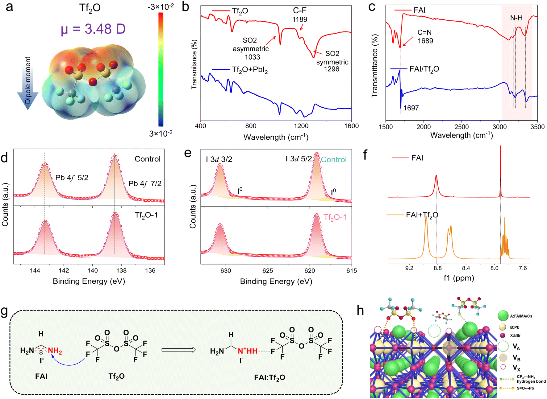 | ||
| Fig. 1 (a) The chemical structure and electrostatic surface potential (ESP) map of Tf2O. (b) FTIR spectrum of pure Tf2O and Tf2O + PbI2 films. (c) FTIR spectra of pure FAI and Tf2O + FAI films. The XPS of (d) Pb 4f and (e) I 3d core levels. (f) 1H NMR spectra of FAI and FAI with Tf2O; f1, magnetic intensity. (g) Schematic of proposed inductive effect between FAI and Tf2O. (h) Schematic representation of the chemical interaction between Tf2O and the perovskite film. | ||
To gain insight into the intermolecular interaction between Tf2O and FAI, 1H nuclear magnetic resonance spectroscopy (1H NMR) was performed, as shown in Fig. 1f. For FAI, two singlet peaks at δ = 7.91 and 8.85 ppm in the NMR spectra correspond to the protons of –CH and –NH2 of pure FAI. These two single peaks imply one uniform chemical environment for the –CH and –NH2 groups in FAI. When FAI was mixed with Tf2O, the two peaks show chemical shifts compared to the proton peaks of FAI, suggesting an inductive effect due to F⋯NH2 hydrogen-bonding interaction between Tf2O and FAI. Intriguingly, the signals for –CH and –NH2 in the FAI spectra are split into multiplets and two peaks by adding Tf2O, which can be ascribed to the positive charges in FAI distributed uniformly in the N–C–N region being polarized due to the formation of a hydrogen bond between CNH and –CF3, resulting in a change in the electronegativity of the two nitrogens. The advantage of the inductive effect is that the polarized FAI can anchor hydrogen iodide to the secondary amine, which can stably move the iodide ion. The intermolecular interaction between Tf2O and FAI is illustrated in Fig. 1g. The interfacial interaction of Tf2O toward the uncoordinated Pb cations and organic cations in the perovskite film would be favorable to the mitigation of non-radiative recombination at the interface, as depicted in Fig. 1h. These results suggest that the inductive effect can stabilize iodide ions on the perovskite film surface, change the interfacial energetic of the perovskite film, and efficiently suppress the degradation of the perovskite film to a certain extent.
To investigate the influence of Tf2O on device performance, we fabricated PSCs with Tf2O-modified perovskite films on a mesoporous device architecture consisting of the following layers: fluorine-doped tin oxide (FTO)/titanium oxide (TiO2)/(CsPbI3)0.05(FA0.85MA0.15Pb(I0.85Br0.15)3)0.95/Tf2O/Spiro-OMeTAD/Au. Considering the insulating property of Tf2O, we carefully regulated the concentration of Tf2O to control the Tf2O residue on top of the perovskite films, as shown in Fig. 2a. The corresponding photovoltaic parameters are shown in Fig. S2 (ESI†). The statistical distribution of PCE values from 18 devices each for the control, Tf2O-1, and Tf2O-5 modified devices confirms that the enhancement in photovoltaic performance arises from the introduction of Tf2O to the perovskite film surface. The optimal concentration for the Tf2O-treated PSCs is obtained at 1 mM. Fig. 2b presents the current density–voltage (J–V) curves of the control and Tf2O-modified PSCs measured under standard AM 1.5G illumination in ambient conditions. The champion control device shows VOC, current density (JSC), FF, and PCE values of 1.088 V, 24.13 mA cm−2, 72.84%, and 19.14%, respectively (Table 1). 1 mM Tf2O-modified PSCs (referred to as Tf2O-1) achieved an overall enhancement in JSC up to 24.68 mA cm−2, a VOC of 1.111 V, and FF of 78.92%, resulting in a remarkable higher PCE of 21.64%. Devices treated with 5 mM Tf2O (referred to as Tf2O-5) yield a lower PCE of 20.45% with a JSC of 24.12 mA cm−2, a VOC of 1.118 V, and a reduced FF of 75.84%. The incident photon-to-electron conversion efficiency (IPCE) spectra of the fabricated devices are shown in Fig. 2c. The integrated JSC for the control, Tf2O-1, and Tf2O-5 modified PSCs are found to be 23.88 mA cm−2, 24.35 mA cm−2, and 23.93 mA cm−2, respectively. Subsequently, we subjected the control and Tf2O-1 modified devices to a long-term stability test, which was monitored by periodically measuring the photovoltaic characteristics of devices that were stored in an N2-filled glovebox. As shown in Fig. 2d and S3 (ESI†), the Tf2O-1 modified device shows outstanding tolerance, retaining 94% of its initial PCE after 1800 h of storage. The control device shows a 27% reduction in PCE only after 500 h. Additionally, the maximum power point (MPP) tracking for 200 s at a voltage of 0.88 V reveals a stable power output, with a stabilized PCE of 21.40% (Fig. S4, ESI†).
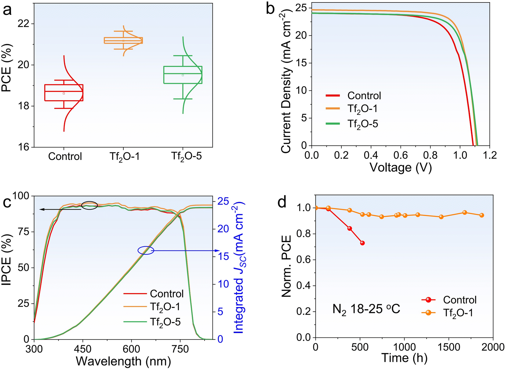 | ||
| Fig. 2 (a) Statistics of PCE depending on 0 mM, 1 mM, 5 mM Tf2O modified devices. (b) J–V curves of control, Tf2O-1, and Tf2O-5 modified PSCs. (c) IPCE and integrated JSC of control, Tf2O-1 and Tf2O-5 modified devices. (d) Long-term stability of control and Tf2O-1 based PSCs in an N2-filled glove box. | ||
| Device | J SC (mA cm−2) | V OC (V) | FF (%) | PCE (%) | ||
|---|---|---|---|---|---|---|
| Control | Best | 24.13 | 1.088 | 72.84 | 19.14 | |
| Average | 24.81 | 1.061 | 71.04 | 18.70 | ||
| Tf2O-1 | Best | 24.69 | 1.111 | 78.92 | 21.64 | |
| Average | 24.73 | 1.109 | 77.17 | 21.17 | ||
| Tf2O-5 | Best | 24.12 | 1.118 | 75.84 | 20.45 | |
| Average | 24.33 | 1.109 | 72.28 | 19.50 | ||
To understand the underlying reason behind the photovoltaic performance of Tf2O-modified PSCs, various characterizations were conducted on the control and Tf2O-modified perovskite films. Surface photovoltage (SPV) measurement was carried out to monitor the changes in interfacial energetics caused by the generation and redistribution of photoexcited charge carriers in semiconductors. As illustrated in Fig. 3a, bandgap-related knees at 1.54 eV, 1.54 eV, and 1.55 eV can be found in control, Tf2O-1, and Tf2O-5 modified films prepared on glass, respectively. It should be noted that the perovskite material used in our study is a weak n-type film:43 the photogenerated electrons spontaneously transfer from bulk to the buried interface, leaving holes and positive ions on the free surface and generating an internal electric field pointing to the buried interface. Fig. 3b depicts the light-intensity-dependent SPV of control, Tf2O-1, and Tf2O-5 modified perovskite films. Notably, the difference in SPV response is attributed to the different concentrations of Tf2O on the perovskite film. The absolute values of SPV in Tf2O-1 modified film (∼90 eV) were significantly higher than in the control film without Tf2O modification (∼40 eV), indicating a greater built-in electric field (BIEF) in Tf2O-1 modified film. By raising the concentration of Tf2O to 5 mM, the absolute value of the SPV is further increased to ∼150 eV. As can be seen in Fig. 3c, there is a clear positive association between SPV and the VOC of Tf2O-modified devices. Thus, the SPV is intimately associated with the related VOC. With Tf2O-1 and Tf2O-5 modification, the VOC of the control device gradually increased from 1.088 V to 1.119 V. Furthermore, we can visualize the Tf2O distribution with nanoscale resolution using Kelvin probe force microscopy (KPFM). As shown in Fig. 3d–f and S5 (ESI†), the WF of control, Tf2O-1, and Tf2O-5 films are calculated to be −375.6 mV, −331.3 mV, and −264.3 mV, respectively. Accordingly, the change in WF in transition metal oxide and perovskite materials is correlated to the cation state and point defect concentrations.44 As shown in Fig. 3d–f, a uniform WF distribution was found in the Tf2O-1 modified film, indicating more effective passivation in comparison to Tf2O-5. Whereas the non-uniform WF of Tf2O-5 film might be attributed to the formation of monohydrate at high concentration levels, as illustrated in the atomic force microscopy (AFM) and scanning electron microscopy (SEM) (Fig. S6, ESI†). These results indicate that adding Tf2O at the perovskite surface raises the valence-band edge of perovskite with respect to the Fermi level. Overall, the surface potential reveals larger band bending at the Tf2O-1 modified interface and a significantly larger total charge depletion width at the heterointerface compared to the control.
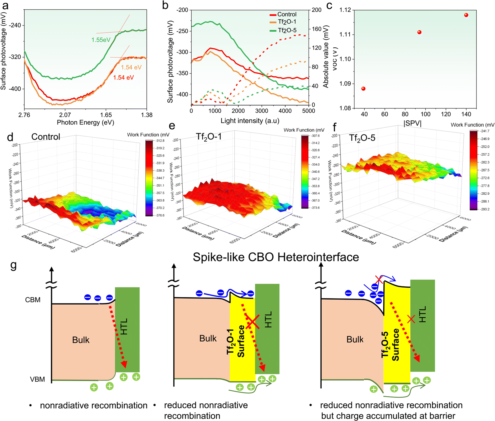 | ||
| Fig. 3 (a) SPV spectra of control, Tf2O-1, and Tf2O-5 treated films. (b) Light-intensity-dependent SPV of samples under light irradiation. (c) Interval plot of device VOC as a function of SPV absolute value. WF maps of (d) control film, (e) Tf2O-1 modified film, and (f) Tf2O-5 modified film, respectively. (g) Schematic of proposed band alignment at the heterointerface through Tf2O-1 and Tf2O-5 modification. | ||
According to the conclusions drawn from SPV and WF measured above, a schematic in Fig. 3g is drawn to understand the role of the spike structure in the complete device. It is known that a cliff does not impede the photogenerated electrons; however, it lowers the activation energy for carrier recombination at the interface, which results in a decrease in VOC. The cliff can act as a barrier against injected electrons under forward bias, resulting in the recombination of a majority of carriers via defects at the interface. In contrast, a spike-like CBO was introduced when perovskite was treated with Tf2O, which increases the energy for carrier recombination at the interface, improving the VOC and overall PCE. Interestingly, we also observed a considerable up-shift in WF in Tf2O-5 modified film, which can cause a large CBO at the heterointerface, forming a potential well to trap charges/holes at the heterointerface that traps charges and increases the resistance to hole extraction, thereby reducing the FF. This result is very consistent with a recent study by Yang's group, in which substantial band bending might result in increased resistance and a lower FF.45 Considering the inductive effect of Tf2O, we believe that the changes in spike-like CBO in Tf2O-1 and Tf2O-5 modified films can be attributed to the polarization of the FAI, as demonstrated by the NMR and XPS results.
To investigate the effect of Tf2O on the carrier recombination kinetics and trap states, we subjected the control and Tf2O-1 films to a series of tests. Fig. 4a provides a comparison of the PL intensity between the control and Tf2O-1 modified films. Clearly, the higher photoluminescence (PL) intensity noted for the Tf2O-1 modified film compared to the control implies a reduction in defect density with Tf2O treatment. Lengthening of carrier lifetime, in the absence of a charge extraction layer, is determined through time-resolved photoluminescence (TRPL) studies (Fig. 4b and Table S1†), where the average lifetime of the Tf2O-1 modified film is 587.9 ns, up from 181.1 ns for the control. The trap densities of the control and Tf2O-modified devices determined from space-charge-limited-current (SCLC) (Fig. 4c) are calculated to be 1.2 × 1016 cm−3 for the control and 5.5 × 1015 cm−3 for the Tf2O-1 modified devices, respectively. Additionally, the light-intensity-dependent J–V characteristics were also evaluated. The VOC and the seminatural logarithm of light intensity exhibit a linear fitting relationship. In general, the device exhibits negligible trap-assisted Shockley–Read–Hall (SRH) recombination when the slope is close to 1 kT/q. The slopes are calculated to be 1.55 kT/q and 1.22 kT/q for the control and Tf2O-1 modified devices, respectively, where k is the Boltzmann constant, q is the elemental charge, and T is the temperature. The lower slope of the Tf2O-1 modified device implies a reduction in trap-assisted SRH recombination compared to the control device. Consequently, the treatment of perovskite film with Tf2O-1 can effectively suppress SRH recombination and enhance the carrier lifetime due to the chemical interaction between Tf2O and the perovskite film. In line with the TRPL and SCLC results, transient photovoltage (TPV) decay curves of the modified devices also show an increasing trend from 0.057 ms to 0.085 ms when using Tf2O modification (Fig. S7, ESI†). X-ray diffraction (XRD) measurements were conducted, as shown in Fig. S8 (ESI†). The full width at half-maximum (FWHM) of the XRD peak is estimated from a Gaussian curve fitting. The FWHM of both control and Tf2O-modified film is calculated to be 0.119, indicating that the chemical interaction with Tf2O does not influence the crystallinity of the perovskite films.
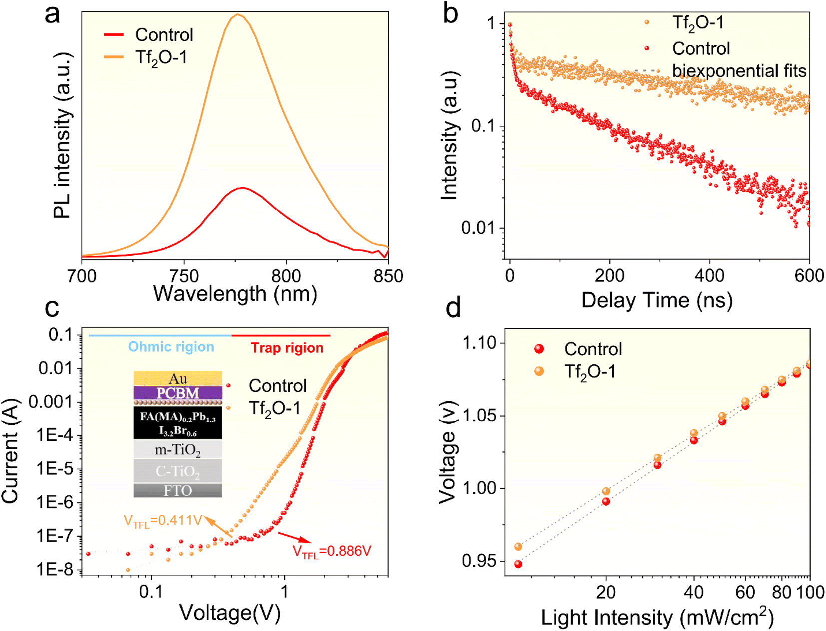 | ||
| Fig. 4 (a) Steady-state and (b) time-resolved photoluminescence (TRPL) of control and Tf2O-1 modified perovskite films prepared on glass. (c) Dark J–V curves for control and Tf2O-1 modified electron-only devices based on FTO/ETL/perovskite/PCBM/Au. (d) VOCversus light intensity for the control and Tf2O-1 modified devices. | ||
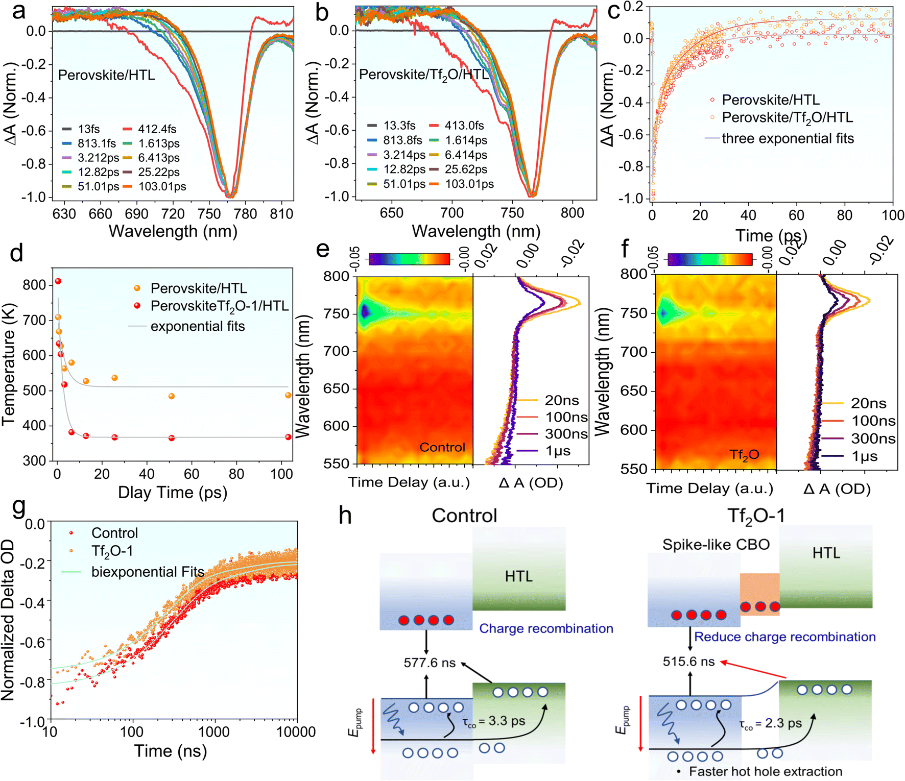
We performed nanosecond-(ns) and femtosecond-(fs) transient absorption (TA) measurements to understand the photoinduced carrier dynamics of Tf2O-1 modified perovskite film, including charge-carrier injection and hot hole carrier (HC) extraction. We employed fs-TA to understand the influence of Tf2O on hole transfer at the interface of TiO2/perovskite, as revealed in Fig. 5a–d. All samples of the perovskite film were excited at 475 nm under an excitation energy of 14 μJ cm−2. Fig. S9† exhibits the 2D pseudo-color plots of the fs-TA spectra of perovskite/HTL and perovskite/Tf2O/HTL films. Notably, a photobleaching (PB) band at 766 nm indicates the band state filling between the valence band edge and the conduction band edge of the perovskite film. Scans at various delays extracted from pseudo-color plots are presented in Fig. 5a and b. The high-energy tails gradually become narrower with time due to the hole-carrier cooling process, which can be evaluated with the carrier temperature (Tc). Accordingly, Tc can be extracted by fitting the high-energy tail above the bandgap of the TA spectra with the Maxwell–Boltzmann distribution function of exp (Ef − E/kBTc), where Ef is the Fermi level, and kB is the Boltzmann constant.46,47 As revealed in Fig. 5c, the perovskite/HTL shows a slower HC temperature decay of 3.3 fs, whereas the perovskite/Tf2O/HTL film presents a faster HC temperature decay of 2.3 fs. The faster HC cooling process presented in perovskite/Tf2O/HTL can break the thermal photons of hot carriers, thereby improving the device's performance. The HC relaxation dynamics contain a dominant three-exponential decay component due to the recombination of charge carriers. As shown in Fig. 5d, the fs-TA curves were well fitted by a three-exponential-function equation, I(t) = A1![[thin space (1/6-em)]](https://www.rsc.org/images/entities/char_2009.gif) exp(−x/τ1) + A2exp(−x/τ2) + A3exp(−x/τ3), where τ1 refers to charge-carrier trapping at the perovskite interface, τ2 is HC transport from the perovskite to the hole transport layer (HTL), and τ3 is the carrier recombination time.48,49
exp(−x/τ1) + A2exp(−x/τ2) + A3exp(−x/τ3), where τ1 refers to charge-carrier trapping at the perovskite interface, τ2 is HC transport from the perovskite to the hole transport layer (HTL), and τ3 is the carrier recombination time.48,49
 | ||
| Fig. 5 Normalized fs-TA kinetics of perovskite/HTL without (a) or with (b) Tf2O-1 treatment. (c) Normalized fs-TA spectra at early delays of perovskite/HTL and perovskite/Tf2O/HTL. (d) Hot carrier temperature (TC) as a function of delay times for films. 2D color plot/normalized fs-TA kinetics of ns-TA of (e) perovskite/HTL and (f) perovskite/Tf2O/HTL. (g) Normalized ns-TA delay spectra of perovskite/HTL and perovskite/Tf2O/HTL. (h) Schematic illustration depicting the effect of Tf2O on the charge-carrier dynamics. | ||
The fitting details and values for fs-TA are summarized in Table S3.† Clearly, the large portion of τ1 implies that the trap filling process is dominant in the HC relaxation dynamics. The decreased τ1 in the Tf2O-modified films compared to the film without Tf2O indicates a faster trap filling process, suggesting a larger splitting in the quasi-Fermi energy levels and a larger charge depletion width in the perovskite film, which is consistent with the results of SPV measurement. Furthermore, the decreased τ2 and τ3 indicate that the entire recombination process can be effectively suppressed with the help of Tf2O. Therefore, these results suggest that the dipolar layer of Tf2O can provide a thermodynamic driving force by tuning the heterointerface, thus promoting hole transport dynamics. To understand the modified heterointerface on the charge-carrier transport, we also studied the ns-TA measurement perovskite with and without Tf2O prepared on glass/TiO2 substrates. Similarly, a photobleaching peak at 766 nm is obtained in the ns-TA spectra (Fig. 5e and f). The corresponding kinetic decay traces of PB at 766 nm were studied. The lifetime of the perovskite films with electron transporting layers (ETLs) was fitted by a single-exponential function, as shown in Fig. 5g. The decay lifetime values of control and Tf2O-modified film are calculated to be 577.6 ns and 515.6 ns, respectively. Therefore, the ETL/perovskite interfacial charge recombination velocity can be evaluated to be 1.7 × 10⁷ and 1.94 × 10⁷ s−1 based on κ = 1/τ.50 The decreased charge recombination velocity of Tf2O-modified film demonstrates the fast charge-carrier injection from the perovskite film to ETLs and thus effectively reduces the charge aggregation and non-radiative recombinations at the ETL interface. As a result, both the fs-TA and ns-TA measurements confirm that the Tf2O-induced spike-like CBO can efficiently promote the photoinduced charge/hole transfer at the interfaces, which could provide a reasonable explanation for the improved VOC, FF, and PCE of the Tf2O-modified device. Fig. 5h depicts the proposed mechanism of spike-like CBO offered by Tf2O. A modest favorable spike-like CBO rises in the Tf2O-modified perovskite surface, acting as a barrier to suppress the interfacial non-radiative recombination and enhancing the hot hole carrier extraction at the interface, thus enhancing the device performance and stability.
Conclusion
In summary, we have demonstrated an effective strategy to construct spike-like energy band alignment at the heterointerface between a perovskite film and HTL as an approach to reduce the potential loss in PSCs. As a result, the Tf2O-modified device exhibits an improved PCE of 21.6% due to the reduction of non-radiative recombination. We found that the spike-like energy band alignment at the heterointerface of perovskite film with Tf2O modification can promote rapid charge-carrier injection and suppress non-radiative recombination at the interface. This work provides important insights into interfacial energetic engineering in PSCs to achieve both high efficiency and long-term stability.Experimental section
Materials
Cesium iodide (CsI), lead iodide (PbI2), lead bromide (PbBr2), formamidiniumiodide (FAI), N2,N2,N2′,N2′,N7,N7,N7′,N7′-octakis(4-methoxyphenyl)-9,9′-spirobi[9H-fluorene]-2,2′,7,7′-tetramine (Spiro-OMeTAD) and methylammonium bromide (MABr) were supplied by Xi'an Polymer Light Technology Corp. Trifluoromethanesulfonic anhydride (Tf2O) was purchased from Energy Chemical. Fluorine-doped tin oxide (FTO)-coated glass substrates, TiO2 paste, acetylacetone, titanium diisoproxide bis(acetylacetonate) 75% in isopropyl alcohol, isopropanol (IPA), N,N′-dimethylformamide (DMF), dimethyl sulfoxide (DMSO), acetone, absolute ethanol, and chlorobenzene (CB) were supplied by Aladdin. 4-Tert-butylpyridine (tBP), bis(trifluoromethylsulfonyl) imide lithium salt (LiTFSI), acetonitrile (ACN), tris(2-(1H-pyrazol-1-yl)-4-tert-butylpyridine)-cobalt(III) tris(bis(trifluoromethyl-sulfonyl) imide) (FK 209), were purchased from Sigma-Aldrich.Precursor solution preparation
Compact TiO2 (c-TiO2): a mixture of 0.6 mL of titanium diisopropoxide bis(acetylacetonate) and 0.4 mL of acetylacetonate in 9 mL of anhydrous ethanol was stirred overnight. It was filtered with an organic filter head before use. Mesoporous TiO2 (m-TiO2): a mixture of 1 g of TiO2 paste in 6 g of anhydrous ethanol was stirred overnight. Perovskite precursor solution: a mixture of 553.4 mg of PbI2, 73.2 mg of PbBr2, 194.4 mg of FAI, 22.3 mg of MABr, and 18.2 mg of CsI in a mixed solvent of DMF and DMSO (v:v = 5:1) was stirred overnight. Hole transport layer (HTL): 85 mg of Spiro-OMeTAD was mixed in 1 mL of CB with additives of 28.8 μL of t-BP, 17.8 μL of LiTFSI (520 mg mL−1 in ACN), 6.5 μL of FK209 (300 mg mL−1 in ACN).
Device fabrication
The FTO substrates (7 Ω) were cleaned ultrasonically for 20 min using detergent water, deionized water, acetone, and ethanol before drying in an oven for 30 min at 65 °C. The cleaned FTO glasses were coated with a c-TiO2 layer and then exposed to 450 °C of annealing treatment for 1 h. After that, m-TiO2 layers were deposited on the FTO/c-TiO2 substrates with a thermal annealing treatment at 500 °C. Subsequently, 30 μL of perovskite solution was spin-coated onto the FTO/c-TiO2/m-TiO2 substrates at 1000 rpm for 10 s and 5000 rpm for 30 s. During the 2nd step, 110 mL of CB was poured on the spinning substrate 15 s before the end of the program. And then the substrates were annealed first at 60 °C for 5 min and then at 100 °C for 30 min. For the Tf2O-treated devices, different concentrations of Tf2O in IPA were spin-coated on the substrate at a speed of 3000 rpm for 20 s and left for 30 min. Subsequently, the HTL precursor solution was spin-coated onto the FTO/c-TiO2/m-TiO2/with or without Tf2O substrates at 4500 rpm for 30 s. A gold layer was thermally evaporated under a high vacuum (<2.0 × 10⁻⁴ Pa) to complete the fabrication of the devices.Devices characterization
All the devices for characterization were made using a metal mask with an active area of 0.0625 cm2. A Newport solar simulator (model 91160) and a Keithley 2400 source/meter were used to simulate and measure the current–voltage characteristics under 100 mW cm−2 (AM 1.5G illumination). Incident photon-to-current conversion efficiency (IPCE) spectra were recorded using a computer-controlled setup consisting of a xenon light source (Spectral Products ASB-XE-175), a monochromator (Spectral Products CM110), and a potentiostat (LabJack U6 DAQ board), calibrated by a certified reference solar cell (Fraunhofer ISE). The transient photovoltage (TPV) and the change in photovoltage with light intensity were measured by an electrochemical workstation (Zennium X, Zahner). In the first-principles calculations (DFT), electron–ion interactions of Tf2O were described using the Vienna ab initio Simulation Package (VASP) and Projected Enhanced Wave (PAW) methods. The Fourier-transform infrared spectroscopy (FTIR) spectroscopy was carried out using a Nicolet iS10 (Thermo Fisher). The 1H NMR and 13C NMR spectra were performed on a Bruker Ascend 400 MHz spectrometer. A vibrating Kelvin probe (probe diameter = 2 mm) (KP Technology, UK) was used to determine the surface potential. Samples were prepared by depositing perovskite films (thickness around 500 nm) on FTO glass. Ambient SPV measurements were done under illumination from a 150 W quartz tungsten halogen lamp, where the intensity was varied linearly by controlling the power supplied to the lamp. The steady-state photoluminescence (PL) measurement was performed using a spectrometer (FLS1000, Edinburgh Instruments). The time-resolved PL (TRPL) decay transients were measured using a picosecond pulse diode laser (EPL-470). Nanosecond transient absorption (TA) spectroscopy was investigated with a spectrometer (LP980, Edinburgh Instruments). Femtosecond transient absorption (fs-TA) measurements were performed for the films using a multipass amplified Ti:sapphire laser (800 nm laser pulses with a 3.5 mJ per pulse; pulse width of ∼120 fs with a repetition rate of 2 kHz, Astrella from coherent; the detection time delay was in the range of 8.5 ns in conjunction with Helios spectrometers). X-ray photoelectron spectroscopy (XPS) was performed using a scanning XPS microprobe (K-Alpha+). X-ray diffraction (XRD) patterns of films were measured with a TTR-18KW diffractometer, with Cu Kα radiation (λ = 0.15405 nm) operated at 10000 W power (40 kV, 250 mA). The surface morphology of the films was characterized by scanning electron microscopy (SEM) and atomic force microscopy (AFM) with the tapping mode. The space-charge-limited-current (SCLC) measurements were performed by collecting the I–V characteristics of the devices under dark conditions. Fourier-transform infrared (FTIR) spectroscopy was carried out using a Nicolet iS10 (Thermo Fisher).
Author contributions
Y. H. and L. X. conceived the project, and R. W. signed the experiments, analyzed the data, and prepared the manuscript. R. W. carried out the film deposition and device fabrication. R. W. carried out the characterizations, including SEM, XRD, and T. W. conducted the PL and TRPL tests. C. G. carried out the XPS measurements and analysis. All authors discussed the results and commented on the manuscript. Y. H. supervised the project and L. X. revised the manuscript.Conflicts of interest
The authors declare that they have no known competing financial interests or personal relationships that could have appeared to influence the work reported in this paper.Acknowledgements
L. Xie thanks the National Natural Science Foundation of China (22209144), the Project of Natural Science Foundation of Yunnan (202201AT070114 and 202201AU070030). Y. Hua thanks the National Natural Science Foundation of China (22065038), the Key Project of Natural Science Foundation of Yunnan (KC10110419), High-Level Talents Introduction in Yunnan Province (C619300A010), the Fund for Excellent Young Scholars of Yunnan (K264202006820), International Joint Research Center for Advanced Energy Materials of Yunnan Province (202003AE140001), the Program for Excellent Young Talents of Yunnan University and Major Science and Technology Project of Precious Metal Materials Genetic Engineering in Yunnan Province (No. 2019ZE001-1 and 202002AB080001-6) for financial support.Notes and references
- B. Cai, Y. Xing, Z. Yang, W.-H. Zhang and J. Qiu, Energy Environ. Sci., 2013, 6, 1480–1485 RSC.
- N. Li, X. Niu, L. Li, H. Wang, Z. Huang, Y. Zhang, Y. Chen, X. Zhang, C. Zhu, H. Zai, Y. Bai, S. Ma, H. Liu, X. Liu, Z. Guo, G. Liu, R. Fan, H. Chen, J. Wang, Y. Lun, X. Wang, J. Hong, H. Xie, D. S. Jakob, X. G. Xu, Q. Chen and H. Zhou, Science, 2021, 373, 561–567 CrossRef CAS.
- M. Kim, J. Jeong, H. Lu, T. K. Lee, F. T. Eickemeyer, Y. Liu, I. W. Choi, S. J. Choi, Y. Jo, H. B. Kim, S. I. Mo, Y. K. Kim, H. Lee, N. G. An, S. Cho, W. R. Tress, S. M. Zakeeruddin, A. Hagfeldt, J. Y. Kim, M. Grätzel and D. S. Kim, Science, 2022, 375, 302–306 CrossRef CAS.
- Y. Zhao, Z. Qu, S. Yu, T. Shen, H. Deng, X. Chu, X. Peng, Y. Yuan, X. Zhang and J. You, Science, 2022, 534, 531–534 CrossRef.
- J. Jeong, M. Kim, J. Seo, H. Lu, P. Ahlawat, A. Mishra, Y. Yang, M. A. Hope, F. T. Eickemeyer, M. Kim, Y. J. Yoon, I. W. Choi, B. P. Darwich, S. J. Choi, Y. Jo, J. H. Lee, B. Walker, S. M. Zakeeruddin, L. Emsley, U. Rothlisberger, A. Hagfeldt, D. S. Kim, M. Grätzel and J. Y. Kim, Nature, 2021, 592, 381–385 CrossRef CAS.
- H. Min, D. Y. Lee, J. Kim, G. Kim, K. S. Lee, J. Kim, M. J. Paik, Y. K. Kim, K. S. Kim, M. G. Kim, T. J. Shin and S. Il Seok, Nature, 2021, 598, 444–450 CrossRef CAS.
- NREL, Best Research-Cell Efficiencies, https://www.nrel.gov/pv/cell-efficiency.html, accessed 20 November 2022 Search PubMed.
- O. J. Sandberg, J. Kurpiers, M. Stolterfoht, D. Neher, P. Meredith, S. Shoaee and A. Armin, Adv. Mater. Interfaces, 2020, 7, 2000041 CrossRef CAS.
- X. L. Xu, L. B. Xiao, J. Zhao, B. K. Pan, J. Li, W. Q. Liao, R. G. Xiong and G. F. Zou, Angew. Chem., Int. Ed., 2020, 59, 19974–19982 CrossRef CAS.
- T. Wu, X. Liu, X. Luo, H. Segawa, G. Tong, Y. Zhang, L. K. Ono, Y. Qi and L. Han, Nano-Micro Lett., 2022, 14, 99 CrossRef CAS.
- Y.-N. Lu, J. X. Zhong, Y. Yu, X. Chen, C. Y. Yao, C. Zhang, M. Yang, W. Feng, Y. Jiang, Y. Tan, L. Gong, X. Wei, Y. Zhou, L. Wang and W.-Q. Wu, Energy Environ. Sci., 2021, 14, 4048–4058 RSC.
- M. Stolterfoht, C. M. Wolff and D. Neher, Nat. Energy, 2018, 3, 847–854 CrossRef CAS.
- M. Daboczi, J. Kim, J. Lee, H. Kang, I. Hamilton, C. T. Lin, S. D. Dimitrov, M. A. McLachlan, K. Lee, J. R. Durrant and J. S. Kim, Adv. Funct. Mater., 2020, 30, 2001482 CrossRef CAS.
- D. Zheng, R. Peng, G. Wang, J. L. Logsdon, B. Wang, X. Hu, Y. Chen, V. P. Dravid, M. R. Wasielewski, J. Yu, W. Huang, Z. Ge, T. J. Marks and A. Facchetti, Adv. Mater., 2019, 31, 1903239 CrossRef CAS.
- Y. Tan, X. Chang, J. X. Zhong, W. Feng, M. Yang, T. Tian, L. Gong and W.-Q. Wu, CCS Chem., 2022, 1–15 Search PubMed.
- Z. Lin, Chem. Phys., 2022, 554, 111422 CrossRef CAS.
- Z. Li, C. Xiao, Y. Yang, S. P. Harvey, D. H. Kim, J. A. Christians, M. Yang, P. Schulz, S. U. Nanayakkara, C. S. Jiang, J. M. Luther, J. J. Berry, M. C. Beard, M. M. Al-Jassim and K. Zhu, Energy Environ. Sci., 2017, 10, 1234–1242 RSC.
- S. Zhang, Z. Hu, J. Zhang, X. Jia, J. Jiang, Y. Chen, B. Lin, H. Jiang, B. Fang, N. Yuan and J. Ding, J. Power Sources, 2019, 438, 226987 CrossRef CAS.
- E. Bi, Z. Song, C. Li, Z. Wu and Y. Yan, Trends Chem., 2021, 3, 575–588 CrossRef CAS.
- D. Wei, F. Ma, R. Wang, S. Dou, P. Cui, H. Huang, J. Ji, E. Jia, X. Jia, S. Sajid, A. M. Elseman, L. Chu, Y. Li, B. Jiang, J. Qiao, Y. Yuan and M. Li, Adv. Mater., 2018, 30, 1707583 CrossRef.
- J. Yang, W. Tang, R. Yuan, Y. Chen, J. Wang, Y. Wu, W. J. Yin, N. Yuan, J. Ding and W.-H. Zhang, Chem. Sci., 2021, 12, 2050–2059 RSC.
- H. Wang, F. Zhang, Z. Li, J. Zhang, J. Lian, J. Song, J. Qu and W. Y. Wong, Chem. Eng. J., 2020, 395, 125062 CrossRef CAS.
- D. S. Mann, Y. H. Seo, S. N. Kwon and S. I. Na, J. Alloys Compd., 2020, 812, 152091 CrossRef CAS.
- Y. Sun, J. Zhang, H. Yu, J. Wang, C. Huang and J. Huang, Chem. Eng. J., 2021, 420, 129579 CrossRef CAS.
- L. Yang, J. Feng, Z. Liu, Y. Duan, S. Zhan, S. Yang, K. He, Y. Li, Y. Zhou, N. Yuan, J. Ding and S. Liu, Adv. Mater., 2022, 34, 2201681 CrossRef CAS.
- D. Koo, Y. Cho, U. Kim, G. Jeong, J. Lee, J. Seo, C. Yang and H. Park, Adv. Energy Mater., 2020, 10, 2001920 CrossRef CAS.
- Y. Li, H. Wu, W. Qi, X. Zhou, J. Li, J. Cheng, Y. Zhao, Y. Li and X. Zhang, Nano Energy, 2020, 77, 105237 CrossRef CAS.
- Y. Deng, X. Li and R. Wang, Sol. Energy Mater. Sol. Cells, 2021, 230, 111242 CrossRef CAS.
- Q. Hu, E. Rezaee, W. Xu, R. Ramachandran, Q. Chen, H. Xu, T. EL-Assaad, D. V. McGrath and Z. X. Xu, Small, 2021, 17, 2005216 CrossRef CAS.
- G. Liu, Y. Zhong, W. Feng, M. Yang, G. Yang, J.-X. Zhong, T. Tian, J.-B. Luo, J. Tao, S. Yang, X.-D. Wang, L. Tan, Y. Chen and W.-Q. Wu, Angew. Chem., Int. Ed., 2022, 61, e202209464 CAS.
- F. Ansari, E. Shirzadi, M. Salavati-Niasari, T. Lagrange, K. Nonomura, J. H. Yum, K. Sivula, S. M. Zakeeruddin, M. K. Nazeeruddin, M. Grätzel, P. J. Dyson and A. Hagfeldt, J. Am. Chem. Soc., 2020, 142, 11428–11433 CrossRef CAS.
- S. Tan, T. Huang, I. Yavuz, R. Wang, T. W. Yoon, M. Xu, Q. Xing, K. Park, D. K. Lee, C. H. Chen, R. Zheng, T. Yoon, Y. Zhao, H. C. Wang, D. Meng, J. Xue, Y. J. Song, X. Pan, N. G. Park, J. W. Lee and Y. Yang, Nature, 2022, 605, 268–273 CrossRef CAS.
- S. Wang, T. Wu, J. Qiu, R. Wang, Z. Zhu, X. Zhang and Y. Hua, EcoMat, 2021, 3, 1–10 CAS.
- R. Zhao, L. Xie, R. Zhuang, T. Wu, R. Zhao, L. Wang, L. Sun and Y. Hua, ACS Energy Lett., 2021, 6, 4209–4219 CrossRef CAS.
- R. Wang, T. G. Sun, T. Wu, Z. Zhu, J. Y. Shao, Y. W. Zhong and Y. Hua, Chem. Eng. J., 2022, 430, 133065 CrossRef CAS.
- T. Wu, R. Zhao, J. Qiu, S. Wang, X. Zhang and Y. Hua, Adv. Funct. Mater., 2022, 32, 2204450 CrossRef CAS.
- R. Yuan, B. Cai, Y. Lv, X. Gao, J. Gu, Z. Fan, X. Liu, C. Yang, M. Liu and W.-H. Zhang, Energy Environ. Sci., 2021, 14, 5074–5083 RSC.
- Y. Huang, T. Liu, C. Liang, J. Xia, D. Li, H. Zhang, A. Amini, G. Xing and C. Cheng, Adv. Funct. Mater., 2020, 30, 2000863 CrossRef CAS.
- W. Yu, X. Sun, M. Xiao, T. Hou, X. Liu, B. Zheng, H. Yu, M. Zhang, Y. Huang and X. Hao, Nano Res., 2022, 15, 85–103 CrossRef CAS.
- S. Purser, P. R. Moore, S. Swallow and V. Gouverneur, Chem. Soc. Rev., 2008, 37, 320–330 RSC.
- M. Cametti, B. Crousse, P. Metrangolo, R. Milani and G. Resnati, Chem. Soc. Rev., 2012, 41, 31–42 RSC.
- Y. Ouyang, X. H. Xu and F. L. Qing, Angew. Chem., Int. Ed., 2018, 57, 6926–6929 CrossRef CAS.
- S. Wu, J. Zhang, Z. Li, D. Liu, M. Qin, S. H. Cheung, X. Lu, D. Lei, S. K. So, Z. Zhu and A. K. Y. Jen, Joule, 2020, 4, 1248–1262 CrossRef CAS.
- M. T. Greiner, L. Chai, M. G. Helander, W. M. Tang and Z. H. Lu, Adv. Funct. Mater., 2012, 22, 4557–4568 CrossRef CAS.
- S. Tan, T. Huang, I. Yavuz, R. Wang, T. W. Yoon, M. Xu, Q. Xing, K. Park, D. K. Lee, C. H. Chen, R. Zheng, T. Yoon, Y. Zhao, H. C. Wang, D. Meng, J. Xue, Y. J. Song, X. Pan, N. G. Park, J. W. Lee and Y. Yang, Nature, 2022, 605, 268–273 CrossRef CAS.
- J. Yin, R. Naphade, P. Maity, L. Gutiérrez-Arzaluz, D. Almalawi, I. S. Roqan, J. L. Brédas, O. M. Bakr and O. F. Mohammed, Nat. Commun., 2021, 12, 1–9 CrossRef.
- J. W. M. Lim, D. Giovanni, M. Righetto, M. Feng, S. G. Mhaisalkar, N. Mathews and T. C. Sum, J. Phys. Chem. Lett., 2020, 11, 2743–2750 CrossRef CAS.
- J. Yin, R. Naphade, P. Maity, L. Gutiérrez-Arzaluz, D. Almalawi, I. S. Roqan, J. L. Brédas, O. M. Bakr and O. F. Mohammed, Nat. Commun., 2021, 12, 3995 CrossRef CAS.
- Q. Wei, J. Yin, O. M. Bakr, Z. Wang, C. Wang, O. F. Mohammed, M. Li and G. Xing, Angew. Chem., Int. Ed., 2021, 60, 10957–10963 CrossRef CAS.
- X. Gong, Q. Sun, S. Liu, P. Liao, Y. Shen, C. Grätzel, S. M. Zakeeruddin, M. Grätzel and M. Wang, Nano Lett., 2018, 18, 3969–3977 CrossRef CAS.
Footnote |
| † Electronic supplementary information (ESI) available. See DOI: https://doi.org/10.1039/d2sc06499e |
| This journal is © The Royal Society of Chemistry 2023 |