
 Open Access Article
 This Open Access Article is licensed under a Creative Commons Attribution-Non Commercial 3.0 Unported Licence
Porosity-dependent photoelectrochemical activity of double-layered TiO2 thin films deposited by spin-coating method†
Kuralay Rustembekkyzy a,
Amir Zholdasbekova,
Alshyn Abduvalovb,
Marat Kaikanovb and
Timur Sh. Atabaev*a
a,
Amir Zholdasbekova,
Alshyn Abduvalovb,
Marat Kaikanovb and
Timur Sh. Atabaev*a
aDepartment of Chemistry, Nazarbayev University, Astana 010000, Kazakhstan. E-mail: timur.atabaev@nu.edu.kz; Tel: +7 7172-70-60-26
bDepartment of Physics, Nazarbayev University, Astana 010000, Kazakhstan
First published on 24th November 2023
Abstract
Photoelectrochemical (PEC) cells made of low-cost, chemically stable, and abundant materials are crucial for green hydrogen production. In this regard, the fabrication of porous films with high light trapping ability and a large contact area is crucial for the production of efficient PEC cells. In this report, anatase TiO2 thin films with a porous double-layered structure were successfully prepared using a conventional spin-coating deposition method. Various amounts of polystyrene spheres were used as a pore-templating agent to control the porosity of the films. A range of characterization techniques, such as scanning electron microscopy, X-ray diffraction, X-ray photoelectron spectroscopy, and photoluminescence were employed to assess the morphology, structural and optical properties of prepared TiO2 films. PEC measurements revealed that prepared double-layered TiO2 thin films exhibit porosity-dependent photocatalytic activity. For example, TiO2 films with an optimized porous structure demonstrated an increase in photocurrent density by a factor of ∼2.23 (to 141.7 μA cm−2) and photoconversion efficiency improvement by a factor of ∼2.14 as compared to non-porous double-layered TiO2 reference films. Absorbance and photoluminescence analysis confirmed that improved PEC activity can be attributed to increased light absorption by the porous structure and reduced charge carrier recombination.
1. Introduction
Metal oxide-based semiconductor thin films are frequently employed in industrial applications due to their versatility, simplicity of fabrication, abundance, and low cost. Among them, TiO2 thin films are particularly popular because they can be utilized for the development of thin film-based solar cells,1,2 gas sensors,3,4 UV detection,5,6 UV screening and protection of solar cells,7 superhydrophilic coatings,8,9 photocatalytic degradation of organic pollutants,10,11 photoelectrochemical (PEC) water splitting,12,13 etc. In general, the efficiency of solar cells, gas sensing devices, photocatalytic, and photoelectrochemical devices is strongly dependent on interfacial contact area, i.e. the greater the latter, the better the device efficiency. Consequently, researchers often use TiO2 in the form of nanotubes, nanowires, nanorods, nanoflowers, and nanoflakes.14–17 However, these nanostructures are frequently prepared under harsh and not environment-friendly conditions, such as the thermal treatment of titanium precursors in acidic environments. Moreover, the active region of these nanostructured substrates is frequently limited to small-sized specimens with several square centimeters, which are unsuitable for large industrial processes. In this regard, a facile methodology for deposition of porous TiO2 thin films with high surface area appears to be promising for industrial scalability.Several methods for deposition of porous TiO2 thin films have been reported in the literature, including spray-pyrolysis deposition,18 the sol–gel method,19 dip-coating,20 inkjet printing combined with low-temperature plasma treatment,21 and spin-coating combined with a dip-coating process.22 Among them, the sol–gel and spin-coating methods appear to be promising due to their simplicity and versatility. However, non-even thickness and non-uniform pores that form as a result of the removal of the polymeric molecules also limit the use of TiO2 films prepared by the sol–gel method. In this regard, the spin-coating process of TiO2 slurry paste with polymeric spheres provides high flexibility in thickness variation (via rotation speed) and control over pore size and density (via selection of polymeric sphere size and quantity). In our study, we used polystyrene spheres (∼350 nm in diameter) as a templating agent to deposit TiO2 films with variable porosity. To the best of the authors' knowledge, porosity-dependent PEC activity testing of double-layered porous TiO2 thin films prepared by spin-coating has not yet been reported in the literature. Hence, the main novelty of our work lies in the systematic exploration of porosity-dependent photoelectrochemical (PEC) activity within double-layered porous TiO2 thin films prepared via spin-coating method. Our findings demonstrate that optimizing surface morphology via pore structure manipulation can significantly enhance PEC activity, thus paving the way for advanced PEC water splitting technologies.
2. Materials and methods
2.1 Materials
Analytical grade reagents were purchased from Merck & Co and used as received. An aqueous solution of polystyrene (PS) particles (∼350 nm, 2.5% w/v) was purchased from Polysciences Inc. Fluorine-doped tin oxide (FTO, 12–16 Ω cm−2) glasses were used as conducting substrates.2.2 First TiO2 layer deposition
A slurry paste containing TiO2 nanoparticles (∼58–60 mg per 1 mL of paste) was prepared according to the reported protocol.23 To form the first compact layer, the paste was deposited on clean FTO glasses using a spin-coating method at 500 rpm (5 s) followed by 5000 rpm (20 s). The films were air-dried for several hours before being thermally annealed at 500 °C for 1 h.2.3 Second porous TiO2 layer deposition
In separate vials, 200 μL and 400 μL of PS particles were air-dried at 60 °C and then dispersed in 100 μL of absolute ethanol. Next, 400 μL of TiO2 paste were added to each vial with PS–ethanol, and these mixtures were stirred at 800 rpm for 24 h to make a homogenous PS-containing paste. Finally, second layers were formed on the top of 1st compact layers by spin-coating at 500 rpm (5 s) followed by 5000 rpm (20 s). For the reference, as-prepared TiO2 slurry paste (without PS) was deposited as a second layer. All samples were thermally annealed at 500 °C for 1 h.2.4 Dip-coating process
In a typical dip-coating process, each substrate was immersed in 5 mL of precursor mixture (100 μL of titanium isopropoxide + 10 mL isopropanol). The substrate was dipped in the solution for 30 min to ensure even penetration of the precursor into the film pores. Afterward, the substrate was withdrawn from the solution, gently rinsed with isopropanol and air-dried. Samples were annealed again at 500 °C for 1 h. As-prepared samples were marked as TO (reference TiO2), TO200 (with 200 μL of PS particles), and TO400 (with 400 μL of PS particles).2.5 Characterization
The morphology of prepared thin films was assessed using a field-emission scanning electron microscope (FE-SEM, ZEISS Crossbeam 540). X-ray diffraction (XRD) patterns were obtained using the Rigaku SmartLab system with a Cu Ka X-ray source. X-ray photoelectron (XPS) spectra were obtained using NEXSA Thermo Scientific monochromated low-power Al Ka X-ray source. Photoluminescence (PL) analyses were performed at 310 nm excitation and absorbance was measured from 280 nm to 600 nm using a Hamamatsu Quantarus-QY absolute PL quantum yield spectrometer equipped with an integrating sphere.2.6 PEC activity testing
The PEC activity of prepared films was assessed using a three-electrode system configuration, i.e. with TiO2 films (working electrodes), Ag/AgCl (reference electrode), and Pt wire (counter electrode). All PEC activity measurements were tested several times with negligible deviation and reported as mean values. Aqueous solution of Na2SO4 (0.1 M) was utilized as electrolyte. Solar light irradiation was provided by the solar simulator (Newport LCS-100 100 W, 1.5 AM, Newport-Spectra Physics GmbH) calibrated to 1 sun using a reference silicon cell. Linear sweep voltammetry (LSV) and chronoamperometry (CA) measurements were carried out by using PalmSens4 potentiostat. Measured potentials V vs. Ag/AgCl were converted to reversible hydrogen electrode (RHE) scale by eqn (1):| ERHE = EAg/AgCl + 0.059 pH + 0.205 | (1) |
Applied-bias photoconversion efficiency (ABPE) was calculated according to the eqn (2):
| ABPE (%) = (Jp (A m−2) × (1.23 − V))/P (W m−2) × 100 | (2) |
3. Results and discussion
Fig. 1 depicts the general fabrication scheme of porous double-layered TiO2 films. In all cases, a dense layer of TiO2 is deposited first, followed by a second layer with variable porosity. Non-porous double-layered TiO2 film was used as a reference. In general, high surface porosity can increase the light scattering effects as well as the contact area at the junction of the semiconductor–electrolyte. On the other hand, surface porosity should be controlled because it leads to the formation of cracks and defects, which limits the flow of charge carriers and increases charge recombination.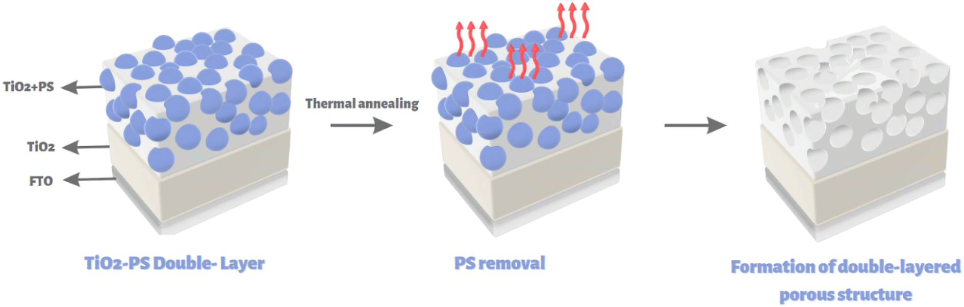 | ||
| Fig. 1 General fabrication scheme of double-layered porous TiO2 films. | ||
Fig. 2A–C shows the SEM images of as-fabricated TO, TO200, and TO400 films. Pore sizes ranging from ∼300 to 350 nm indicate that pores form after the thermal removal of PS particles. The porosity of TO200 and TO400 films are clearly different, with TO400 having a greater number of holes than TO200 (Fig. 2B and C). SEM analysis revealed that the average pore size of TO200 films was 285 ± 40 nm, while the average pore size of TO400 films was around 392 ± 189 nm. The larger mean pore size for TO400 film can be attributed to the merging/localization of several PS particles in a specific region, which results in larger holes after the heat treatment process. However, the deposition of TiO2 films in the absence of PS particles yields a surface without pores and cracks (Fig. 2A). Fig. 2D of TO200 shows the formation of a double-layered structure with bottom nonporous and upper porous layers, and the average thickness of the films was determined to be ∼1.3 μm.
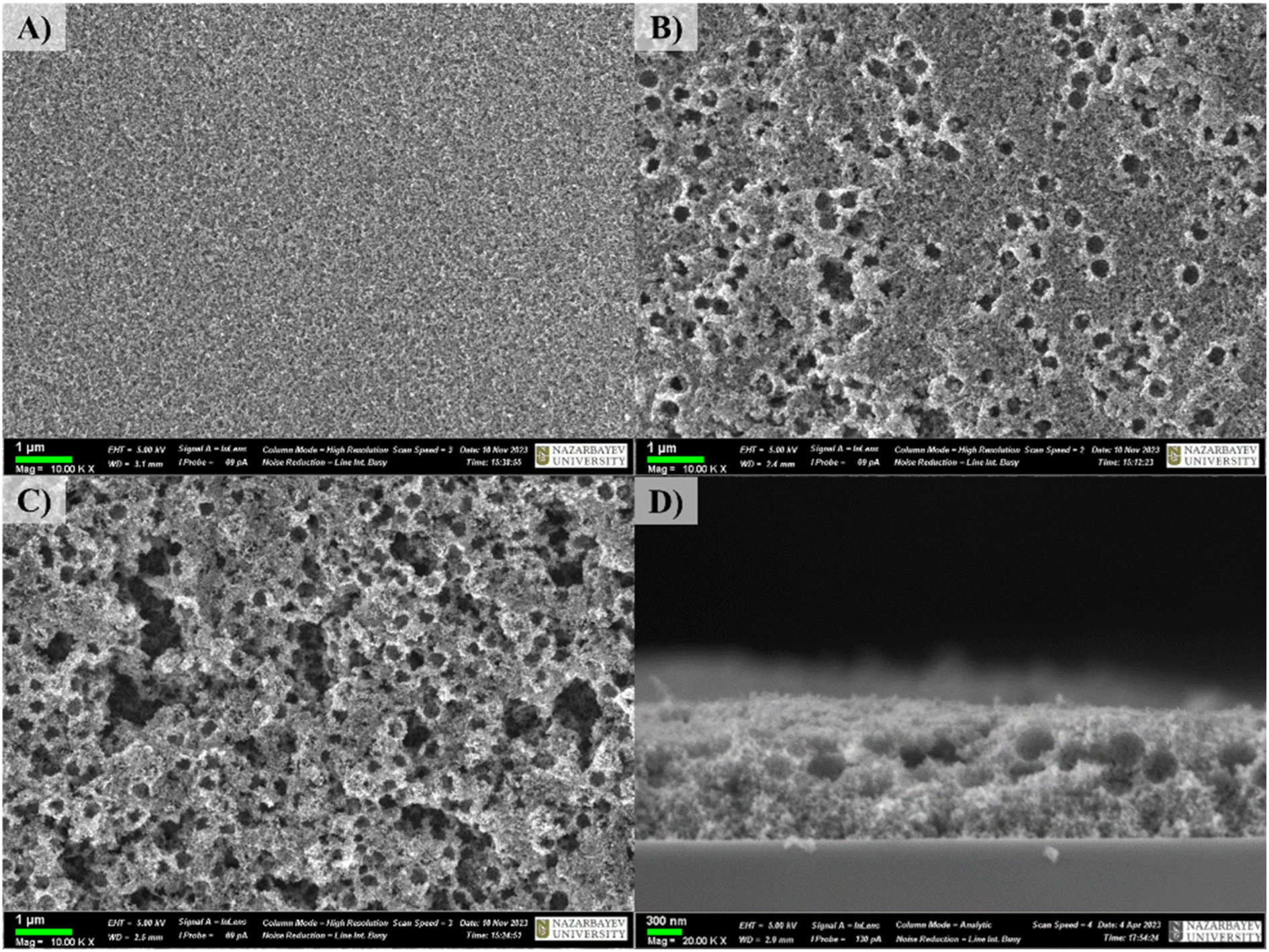 | ||
| Fig. 2 (A–C) Surface SEM images of TO, TO200, and TO400 films, (D) cross-sectional image of TO200 film. | ||
Next, structural properties of the prepared films were evaluated using XRD. Fig. S1 (ESI†) shows the XRD patterns of all three films and bare FTO glass as a reference. Aside from the FTO peaks, all samples displayed two clearly identifiable diffraction peaks at 2θ of ∼25.2° and ∼47.9°, which can be assigned to the (101) and (200) planes of the anatase TiO2 phase (JCPDS card no. 21–1272), respectively.18,22 There were no other peaks observed, indicating the formation of pure anatase TiO2 phase.
PEC activity testing revealed that surface porosity can affect the generated photocurrent density of prepared films. All samples were compared at 1.23 eV vs. RHE. Fig. 3A shows that the photocurrent density of the TO200 film was significantly higher (∼2.23 times) than that of the reference TO films when exposed to solar light. In particular, measured photocurrent densities for TO, TO200, and TO400 films were found to be ∼63.60 μA cm−2, ∼141.7 μA cm−2, and ∼91.70 μA cm−2, respectively. In the dark, all samples had a negligible photocurrent density. The onset potentials were estimated to be ∼0.25 V vs. RHE for TO and TO200 films, and ∼0.31 V vs. RHE for TO400 films. Chronoamperometry analysis (Fig. 3B) displays that the films are structurally stable and that the same photocurrent density can be maintained with periodic light on–off switches. The fact that the photocurrent density of the TO films was the lowest indicates that surface porosity is important in PEC activity. On the other hand, the TO400 sample has a lower photocurrent density than the TO200 sample, suggesting that a film with higher porosity does not always imply better performance. Nevertheless, the photocurrent density of TO400 films was still better than that of bare TO films. According to recent literature analysis (Table 1), the TO200 film was found to be significantly better as compared to some TiO2 nanostructures reported recently. TO200 films, for example, exhibit higher photocurrent density generation than TiO2 nanotube and nanosheet arrays, highlighting their high potential for photocatalytic reactions.
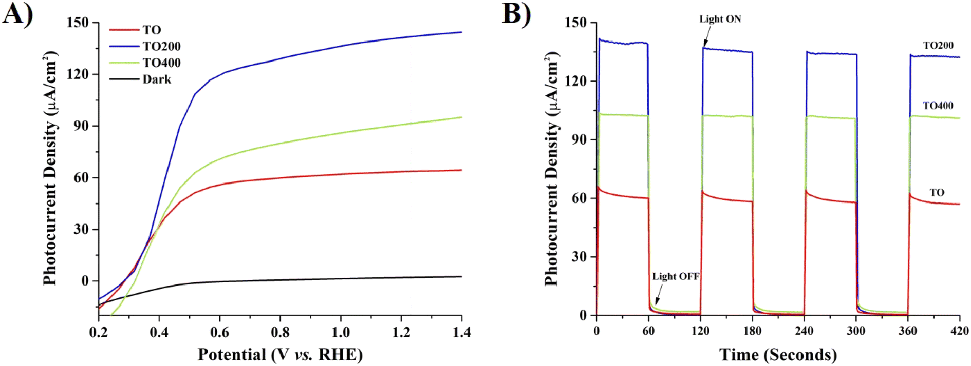 | ||
| Fig. 3 (A) Linear sweep voltammetry (LSV) and (B) chronoamperometry curves of prepared TO, TO200, and TO400 films. | ||
| Composition and structure | Photocurrent density at 1.23 eV vs. RHE | Ref. |
|---|---|---|
| Single-layer inverse-opal like TiO2 thin films deposited by spin-coating | ∼66.50 μA cm−2 | 22 |
| TiO2-rGO thin film deposited by spin-coating | ∼151.3 μA cm−2 | 23 |
| TiO2 thin film (∼300 nm) prepared by pulsed laser deposition | ∼6.100 μA cm−2 | 24 |
| Tin oxide decorated tungsten oxide doped TiO2 nanotubes | ∼59.00 μA cm−2 | 25 |
| Pristine TiO2 nanotubes | ∼51.76 μA cm−2 | 26 |
| Black (reduced) TiO2 nanotubes | ∼126.9 μA cm−2 | 26 |
| TiO2 nanosheet array | ∼36.00 μA cm−2 | 27 |
| TO200 double-layered porous thin film | ∼141.7 μA cm−2 | This work |
The photoconversion efficiency (ABPE) as a function of applied potential was investigated further for all three samples. Fig. 4 depicts typical ABPE parabolic curves, with the TO film yielding 0.036% at 0.518 V vs. RHE, while the TO200 and TO400 films yielded 0.077% and 0.045% vs. 0.567 V vs. RHE, respectively. TO200 clearly has the optimal porosity and the highest ABPE, which are 2.14 and 1.71 times higher than TO and TO400 films, respectively. Hence, controlling surface porosity can be viewed as an effective way to improve the PEC efficiency of photocatalytic thin films.
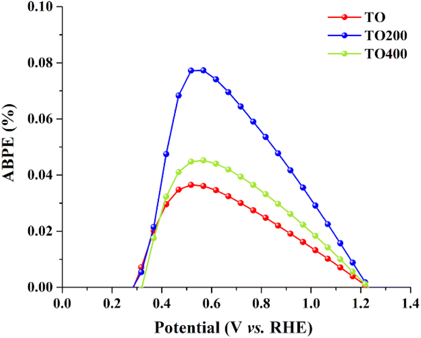 | ||
| Fig. 4 ABPE curves for prepared TO, TO200, and TO400 films. | ||
The improved PEC activity of prepared thin films was investigated further using XPS and PL spectroscopy. It should be noted that while XPS analysis is shown for optimal TO200 film, similar results are obtained for TO and TO400 films as well (data not shown). The binding energies of the Ti 2p1/2 and Ti 2p3/2 peaks (Fig. 5A) are shown to be 464.1 and 458.4 eV, respectively, confirming the presence of Ti4+.27 The core level of O 1s can be fitted to two peaks centered at 531.6 and 529.9 eV (Fig. 5B), which are assigned to adsorbed water and Ti–O, respectively.7,28 Thus, XPS analysis confirmed the formation of pure TiO2 structures in all films, implying that surface porosity should be considered as the only factor responsible for increased PEC activity.
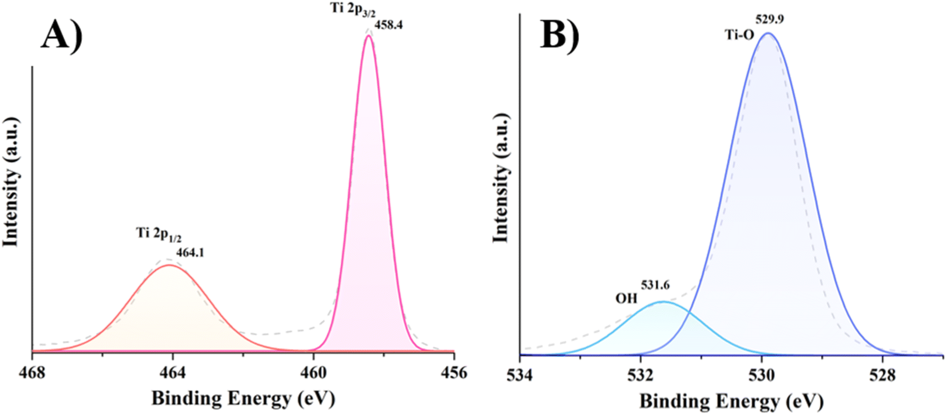 | ||
| Fig. 5 XPS spectra of Ti 2p (A) and O 1s (B) tested with TO200 film. | ||
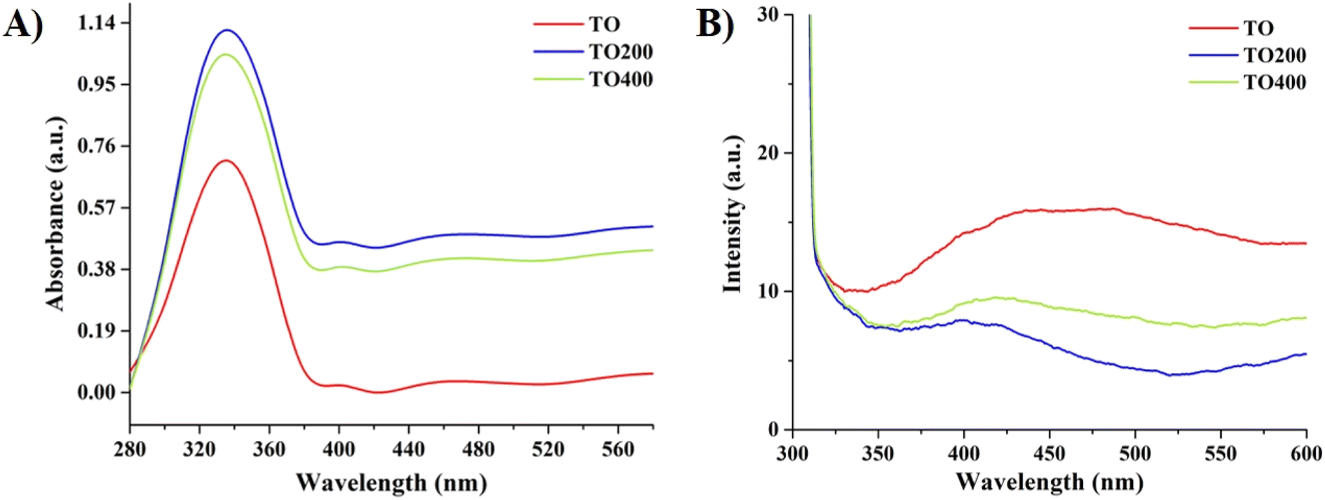
Absorbance and PL measurements of prepared films were subsequently conducted inside the integrating sphere. Fig. 6A shows that all films have a high absorbance up to 390 nm, which corresponds to the bandgap electron transition in the anatase TiO2 structure (cutoff wavelength ∼387 nm). On the other hand, TO200 and TO400 films have higher absorbance in the UV and visible ranges, highlighting the beneficial role of light scattering effects on PEC activity. Typically, TO200 film has slightly higher absorbance than TO400 film, which can be attributed to higher TiO2 content in TO200 films (less porous as compared to TO400). Hence, TO200 film has optimal porosity level which in turn can maximize the light scattering effects.
 | ||
| Fig. 6 (A) Absorbance and (B) photoluminescence of TO, TO200, and TO400 films. | ||
Tauc's equation was applied further to estimate the bandgap values of all prepared films. Fig. S2 (ESI†) yielded the bandgap values of ∼3.211 eV (TO), 3.247 eV (TO200), and 3.242 eV (TO400). All values are close to the anatase TiO2 bandgap value of ∼3.2 eV, indicating that bandgap variation was negligible for all films. Steady-state PL analysis (λexc = 310 nm) was performed to analyze the recombination rate of photogenerated carriers. In general, peaks up to ∼390 nm can be attributed to direct electron–hole recombination, whereas peaks in the blue-green range are caused by intrinsic defect states in TiO2 films.22,29 The TO200 film had a significantly lower emission peak in the UV-visible range when compared to the TO and TO400 films, indicating a lower recombination rate. It should be pointed out that the TO400 sample also demonstrate better PEC activity, absorbance, and a lower recombination rate when compared to the TO reference. Hence, in both cases the porosity level playing an important role in boosting the PEC activity. Despite having more pores, TO400 film has poorer charge transporting properties than TO200 film probably due to a larger number of cracks/larger voids formed during PS particles removal (Fig. 2C) and consequently a higher charge recombination rate, as confirmed by PL analysis. Moreover, it was shown that the pore-size-decreased structure performs better than the pore-size-increased structure in spite of their comparable radiation absorption coefficients.30 Typically, TO400 films have larger-sized voids that are most likely the result of several merged PS particles removed during the thermal treatment. Thus, the porosity level of TO200 film has been found to be optimal in terms of both light absorbance and PEC activity enhancement. It should be noted that these results are valid for PS particles with a diameter of ∼350 nm, and other sizes should be verified separately. Typically, films with different sizes of PS particles and variations in film thickness will be carried out in the forthcoming research.
4. Conclusion
In this study, double-layered porous TiO2 films with improved PEC activity was prepared. We showed that porosity level is important in terms of effective light absorbance/scattering and should be optimized to achieve high PEC activity. Several films with various porosity were prepared and tested for PEC activity. We showed that a film with an optimal porosity level (TO200) can increase PEC activity by more than 2.2 times, with a photocurrent density of ∼141.7 μA cm−2 at 1.23 vs. RHE. Further increase in porosity was found to be detrimental to PEC activity, which can be attributed to the appearance of a bigger amount of small cracks/voids in films. It was suggested that more research in this area is required, typically by varying the size of PS particles and optimizing film thickness.Conflicts of interest
The authors declare that they have no known competing financial interests or personal relationships that could have appeared to influence the work reported in this paper.Acknowledgements
This research was funded by the Science Committee of the Ministry of Science and Higher Education of the Republic of Kazakhstan (Grant no. AP13067604).References
- H. H. T. Vu, T. S. Atabaev, P. C. De, M. A. Hossain, D. Lee, N. N. Dinh, C. R. Cho, H. K. Kim and Y. H. Hwang, TiO2 nanofiber/nanoparticles composite photoelectrodes with improved light harvesting ability for dye-sensitized solar cells, Electrochim. Acta, 2016, 193, 166–171, DOI:10.1016/j.electacta.2016.02.045.
- M. M. Tavakoli, P. Yadav, R. Tavakoli and J. Kong, Surface engineering of TiO2 ETL for highly efficient and hysteresis-less planar perovskite solar cell (21.4%) with enhanced open-circuit voltage and stability, Adv. Energy Mater., 2018, 8, 1800794, DOI:10.1002/aenm.201800794.
- A. Abbasi and J. J. Sardroodi, N-doped TiO2 anatase nanoparticles as a highly sensitive gas sensor for NO2 detection: insights from DFT computations, Environ. Sci.: Nano, 2016, 3, 1153–1164, 10.1039/C6EN00159A.
- P. Singh, M. Mabdulah, S. Sagadevan, C. Kaur and S. Ikram, Highly sensitive ethanol sensor based on TiO2 nanoparticles and its photocatalyst activity, Optik, 2019, 182, 512–518, DOI:10.1016/j.ijleo.2019.01.077.
- M. Cadatal-Raduban, J. Pope, J. Olejníček, M. Kohout, J. A. Harrison and S. M. R. Hasan, Ultraviolet-C photoresponsivity using fabricated TiO2 thin films and transimpedance-amplifier-based test setup, Sensors, 2022, 22, 8176, DOI:10.3390/s22218176.
- M. Chakraborty, E. S. Kadir and R. N. Gayen, Enhanced UV photo-detection properties of graphene oxide incorporated transparent TiO2 thin films in Schottky configuration, Ceram. Int., 2023, 49, 20651–20661, DOI:10.1016/j.ceramint.2023.03.196.
- K. Zhumanova, L. Serik, A. Molkenova and T. S. Atabaev, UV light blocking and conversion by porous europium-doped titanium dioxide (TiO2-Eu) thin films for potential protection of photovoltaic devices, Mater. Today Chem., 2022, 26, 101171, DOI:10.1016/j.mtchem.2022.101171.
- B. Bharti, S. Kumar and R. Kumar, Superhydrophilic TiO2 thin film by nanometer scale surface roughness and dangling bonds, Appl. Surf. Sci., 2016, 364, 51–60, DOI:10.1016/j.apsusc.2015.12.108.
- A. Seifi, D. Salari, A. Khataee, B. Çosut, L. Ç. Arslan and A. Niaei, Enhanced photocatalytic activity of highly transparent superhydrophilic doped TiO2 thin films for improving the self-cleaning property of solar panel covers, Ceram. Int., 2023, 49, 1678–1689, DOI:10.1016/j.ceramint.2022.09.130.
- X. Yang, Y. Min, S. Li, D. Wang, Z. Mei, J. Liang and F. Pan, Conductive Nb-doped TiO2 thin films with whole visible absorption to degrade pollutants, Catal. Sci. Technol., 2018, 8, 1357–1365, 10.1039/C7CY02614E.
- Lalliansanga, D. Tiwari, S.-M. Lee and D.-J. Kim, Photocatalytic degradation of amoxicillin and tetracycline by template synthesized nano-structured Ce3+@TiO2 thin film catalyst, Environ. Res., 2022, 210, 112914, DOI:10.1016/j.envres.2022.112914.
- R. A. Pawar, D. P. Dubal, S. V. Kite, K. M. Garadkar and V. M. Bhuse, Photoelectrochemical and photocatalytic activity of nanocrystalline TiO2 thin films deposited by chemical bath deposition method, J. Mater. Sci.: Mater. Electron., 2021, 32, 19676–19687, DOI:10.1007/s10854-021-06490-5.
- A. Kot, M. Radecka and K. Zakrzewska, Influence of Er and Yb on photoelectrochemical performance of TiO2 thin film, Appl. Surf. Sci., 2023, 608, 155127, DOI:10.1016/j.apsusc.2022.155127.
- A. M. Elseman, A. H. Zaki, A. E. Shalan, M. M. Rashad and Q. L. Song, TiO2 nanotubes: An advanced electron transport material for enhancing the efficiency and stability of perovskite solar cells, Ind. Eng. Chem. Res., 2020, 59, 18549–18557, DOI:10.1021/acs.iecr.0c03415.
- Z. P. Tshabalala, T. P. Mokoena, M. Jozela, J. Tshilongo, T. K. Hillie, H. C. Swart and D. E. Motaung, TiO2 nanowires for humidity-stable gas sensors for toluene and xylene, ACS Appl. Nano Mater., 2021, 4, 702–716, DOI:10.1021/acsanm.0c02963.
- Q.-R. Zhao, W. Wen, Y. Xia and J.-M. Wu, Photocatalytic activity of TiO2 nanorods, nanowires and nanoflowers filled with TiO2 nanoparticles, Thin Solid Films, 2018, 648, 103–107, DOI:10.1016/j.tsf.2018.01.004.
- G. Deng, X. Kang, Y. Yang, L. Wang and G. Liu, Skin B/N-doped anatase TiO2 {001} nanoflakes for visible-light photocatalytic water oxidation, J. Colloid Interface Sci., 2023, 649, 140–147, DOI:10.1016/j.jcis.2023.06.046.
- M. Ibadurrohman and K. Hellgardt, Morphological modification of TiO2 thin films as highly efficient photoanodes for photoelectrochemical water splitting, ACS Appl. Mater. Interfaces, 2015, 7, 9088–9097, DOI:10.1021/acsami.5b00853.
- Z. Landolsi, I. B. Assaker, D. Nunes, E. Fortunato, R. Martins, R. Chtourou and S. Ammar, Enhanced electrical and photocatalytic properties of porous TiO2 thin films decorated with Fe2O3 nanoparticles, J. Mater. Sci.: Mater. Electron., 2020, 31, 20753–20773, DOI:10.1007/s10854-020-04588-w.
- A. Angulo-Ibáñez, A. M. Goitandia, J. Albo, E. Aranzabe, G. Beobide, O. Castillo and S. Pérez-Yáñez, Porous TiO2 thin film-based photocatalytic windows for an enhanced operation of optofluidic microreactors in CO2 conversion, iScience, 2021, 24, 102654, DOI:10.1016/j.isci.2021.102654.
- T. Homola, Z. Ďurašová, M. Shekargoftar, P. Souček and P. Dzik, Optimization of TiO2 mesoporous photoanodes prepared by inkjet printing and low-temperature plasma processing, Plasma. Chem. Plasma Process., 2020, 40, 1311–1330, DOI:10.1007/s11090-020-10086-y.
- K. Rustembekkyzy, A. Molkenova, M. Kaikanov and T. S. Atabaev, Deposition of inverse opal-like TiO2 thin film with enhanced photoelectrochemical activity by a spin-coating combined with a dip-coating method, Nano Express, 2023, 4, 026001, DOI:10.1088/2632-959X/acd131.
- L. Khamkhash, S. Em, A. Molkenova, Y.-H. Hwang and T. S. Atabaev, Crack-free and thickness-controllable deposition of TiO2–rGO thin films for solar harnessing devices, Coatings, 2022, 12, 218, DOI:10.3390/coatings12020218.
- J. Chen, J. Zhang, M. Ye, Z. Rao, T. Tian, L. Shu, P. Lin, X. Zeng and S. Ke, Flexible TiO2/Au thin films with greatly enhanced photocurrents for photoelectrochemical water splitting, J. Alloys Compd., 2020, 815, 152471, DOI:10.1016/j.jallcom.2019.152471.
- G. Mohammadnezhad, M. M. Momeni and F. Nasiriani, Enhanced photoelectrochemical performance of tin oxide decorated tungsten oxide doped TiO2 nanotube by electrodeposition for water splitting, J. Electroanal. Chem., 2020, 876, 114505, DOI:10.1016/j.jelechem.2020.114505.
- F. Habibi-Hagh, L. J. Foruzin and F. Nasirpouri, Remarkable improvement of photoelectrochemical water splitting in pristine and black anodic TiO2 nanotubes by enhancing microstructural ordering and uniformity, Int. J. Hydrogen Energy, 2023, 48, 11225–11236 CrossRef CAS.
- L. Yang, R. Wang, N. Zhou, L. Jiang, H. Liu, Q. He, C. Deng, D. Chu, M. Zhang and Z. Sun, Construction of p–n heterostructured BiOI/TiO2 nanosheets arrays for improved photoelectrochemical water splitting performance, Appl. Surf. Sci., 2022, 601, 154277, DOI:10.1016/j.apsusc.2022.154277.
- K. Alkanad, A. Hezam, N. Al-Zaqri, M. A. Bajiri, G. Alnaggar, Q. A. Drmosh, H. A. Almukhlifi and L. N. Krishnappagowda, One-step hydrothermal synthesis of anatase TiO2 nanotubes for efficient photocatalytic CO2 reduction, ACS Omega, 2022, 7, 38686–38699, DOI:10.1021/acsomega.2c04211.
- V. S. Anitha, S. S. Lekshmy and K. Joy, Effect of annealing on the structural, optical, electrical and photocatalytic activity of ZrO2–TiO2 nanocomposite thin films prepared by sol–gel dip coating technique, J. Mater. Sci.: Mater. Electron., 2017, 28, 10541–10554, DOI:10.1007/s10854-017-6828-3.
- T. Xie, K. Xu, B. Yang and Y. He, Effect of pore size and porosity distribution on radiation absorption and thermal performance of porous solar energy absorber, Sci. China: Technol. Sci., 2019, 62, 2213–2225, DOI:10.1007/s11431-018-9440-8.
Footnote |
| † Electronic supplementary information (ESI) available. See DOI: https://doi.org/10.1039/d3ra06914a |
| This journal is © The Royal Society of Chemistry 2023 |