DOI:
10.1039/D3RA06722J
(Paper)
RSC Adv., 2023,
13, 34693-34702
Designing an efficient lead-free perovskite solar cell with green-synthesized CuCrO2 and CeO2 as carrier transport materials
Received
3rd October 2023
, Accepted 20th November 2023
First published on 28th November 2023
Abstract
With increased efficiency, simplicity in manufacturing, adaptability, and flexibility, solar cells constructed from organic metal halide perovskite (PVK) have recently attained great eminence. Lead, a poisonous substance, present in a conventional PVK impacts the environment and prevents commercialization. To deal with this issue, a number of toxicity-free PVK-constructed solar cells have been suggested. Nevertheless, inherent losses mean the efficiency conversion accomplished from these devices is inadequate. Therefore, a thorough theoretical investigation is indispensable for comprehending the losses to improve efficiency. The findings of a unique modelling method for organic lead-free solar cells, namely methylammonium tin iodide (MASnI3), are investigated to reach the maximum practical efficiencies. The layer pertinent to MASnI3 was constructed as a sandwich between a bio-synthesized electron transport layer (ETL) of CeO2 and a hole transport layer (HTL) of CuCrO2 in the designed perovskite solar cells (PSCs). In this study, the use of algae-synthesized Au in the back contacts has been proposed. To obtain the maximum performance, the devices are further analyzed and optimized for active layer thickness, working temperature, total and interface defect density analysis, impedance analysis (Z′–Z), and capacitance–voltage (C–V), respectively. An optimal conversion efficiency of 26.60% has been attained for an MASnI3-constructed PSC. The study findings may open the door to a lead-free PSC through improved conversion efficiencies.
1. Introduction
The primary research goal for the decade is the overall augmentation of power conversion efficiency (PCE) of non-toxic, renewable solar cells, as a replacement for conventional fuels. Perovskite solar cells (PSCs) in particular have attracted great interest because of their remarkable qualities, including their extremely high coefficient of absorption, low cost, long charge diffusion length, great electron mobility, low trap state density, low binding energy of excitons, and configurable band gaps.1–5
A perovskite material has an archetypical structure relating to ABX3, where A is likely to be a methylammonium cation (CH3NH3+). A has a very small ionic radius of ∼0.18 nm. B is often Pb or Sn, while X is characteristically a halide.6–8 It should be mentioned that Kojima et al. introduced a noble PSC structure, where CH3NH3PbX3 and Br were used to build the active layer as a halide material, which presented a recorded PCE of up to 3.8%.9 Thenceforth, remarkable progress have been achieved in PSC performance over recent years, but there is still a lot of room for improvement. Suitable material selection with optimum thickness, defectivity, and adequate working temperature in device architectures is critical in improving device effectiveness.
A PSC sustains a lower photocurrent density because of a characteristically thin active layer absorbing markedly low quantities of photons. Interestingly, as the thickness of the perovskite active layer increases, less charge extraction is observed in the device output. Also, reasonable recombination-related loss is observed with increased active layer thickness.8,10 So, selecting a suitable thickness becomes a primary concern amongst others in PSC devices.
Apart from the instability involved, the influence of electrode degradation on perovskite solar cells has also been studied.11 Their stability with Au and Ag as the electrodes in a triple-cation MAPbI3-based PSC were also tested.12 In another study, it can be seen that the degradation of a lead halide PSC was greatly influenced by the hole transport layer and the effect of the metal electrode interfaces was also revealed.13 So, stability based on the electrodes in the PSC design has been studied thoroughly in the reports discussions above.
The perovskite layer is held in a sandwich between the electron (ETL) and hole carrier transport layers (CTLs) in classic PSC architecture (ETL and HTL). Spiro-OMeTAD was used in HTL to maximize effectiveness and stability.14 Concurrently, Liu et al. improved the efficiency of a complex device structure, with an ITO/TiO2/CH3NH3PbI3−xClx/Spiro-OMeTAD/Ag layer structure, by 15.4% by employing contemporary vapour deposition approaches.15 But, due to cost, the Spiro-OMeTAD application is impractical to use, a significant concern in PSC manufacturing.8 To replace this complex structure, we employ similar characteristics of the HTL material CuCrO2 for application in PSC devices. Similarly, TiO2 offers relatively low impacts on charge transportation to the anode; it has a non-matching bandgap with the active layer. Moreover, a green-synthesis approach makes the material economical for perovskite fabrication. Recently, efficiency with reference to a PSC was increased by using CeO2 as an ETL and an annealing treatment, increasing efficiency up to 18.36%.16 Butt et al., synthesized CeO2 nanoparticles (NPs), from petals, a plausible material for ETL in present devices. It is important to highlight that planar heterojunction PSCs are workable substitutes for mesoscopic designs because of their simplicity and ease of production.17,18
Applications of ‘green-synthesized nanomaterials’ from microbes (algae/bacteria//actinomycetes/fungi) and plants in modern science and technology have come to the fore thanks to their sustainability, cost-effectiveness, and low toxicity, together with their eco-friendly properties. United Nations ‘Sustainable development Goal’-7 is directly related to affordability together with clean energy. Applying green-synthesized materials in solar cells with the required photovoltaic parameters will provide clean energy with greater efficiency and affordable cost, achieve economic growth, and alleviate climate change.
The ‘CeO2-NPs’ were prepared from the flowers of Cassia glauca.19 The dried petals (20 g) of the flowers were extracted in dH2O (200 mL) and filtered. The extract (100 mL) was pre-heated (75 °C) with stirring (1000 rpm). The extract was alkylated [pH 9; NaOH (0.1 M)]. Ce(NO3)3·6H2O (5 g) was added to the extract, heated (75 ± 5 °C), stirred (1000 rpm), and finally centrifuged to collect the NPs. The CeO2-NPs were spherical, presenting a lattice constant of 5.42 Å, and a ‘crystallite size’ of 3.20 nm. The delafossite (CuCrO2) was prepared from chelating/complexing Aloe vera extracts,20 where 15 g of dried plant in 100 mL of dH2O was stirred for 1 h (60 °C). Millimole equivalents of both Cu(NO3)2·3H2O (0.241 g) and Cr(NO3)3·9H2O (0.40 g) were separately added to 100 mL of extract, mixed, and heated (80 °C) until a clear solution appeared. The solution was further heated (100–120 °C) to a gelatinous mass, dried completely (150 °C, 12 h), and calcined (500 °C, 6 h).
‘Au-NPs’ were synthesized from Prasiola crispa, an epilithic alga, by bioreduction.21 Briefly, 1 g of dry powder of the alga in HAuCl4 solution (10−3 M, 100 mL) was stirred until the colour changed to purple (12 h). The NPs presented an approximately spherical shape (5–25 nm), a crystallite size of 9.8 nm, lattice fringes of 0.233 nm, and polycrystalline nature. A ‘dynamic light scattering’ study revealed the average diameter to be 10 ± 8.6 nm.
A significant advancement in Pb-based PVK materials has occurred in the last few decades. However, the toxicity of lead remains a primary barrier to the broad adoption of PSCs.22 These issues can be overcome by substituting Sn for Pb, which is toxic-free in nature.23–25 Moreover, MASnI3 material has certain advantages pertaining to its bandgap (∼1.3 eV), which is remarkably smaller than that of a conventional PVK material.26 Its reduced bandgap might be the reason for photon absorption by MASnI3 over a wide spectrum of wavelengths. A wider photon wavelength absorption and narrower bandgap enhance device efficiency (from 1.3 eV). The optimization of defect-less, light-harvesting layers to obtain desired optoelectronic characteristics has more impact on the output of a PSC device.
In the present work, SCAPS-1D, a (1-dimensional) simulator of solar cell capacitance, developed by ELIS, University of Ghent, Belgium was used for investigation of the associated PSC, developed with a drift-diffusion model.27 The advantages of the simulator include a deposition capability pertaining to a maximum of seven semiconducting layers together with the ability to rank virtually all characteristics. The mechanism involves the solving of the Poisson equation besides continuity equations, and the simulations may be done under both dark and light conditions.28 The above-mentioned simulator is also convenient for analysing various models with recombination mechanisms, batch computation with the bulk, and interface defect-level calculation.29 The current simulation is applied to both crystalline and amorphous solar cells.30 The present work applies AM1.5G solar irradiance relating to an analysis of carrier transport processes and electrical outputs for the construction of an optical profile, which could be converted into an electrical model for MASnI3-based PSCs.
2. Simulated device structures
As an innovative approach to the advancement of the device, we propose the previous work by Sarkar et al. to find the HTL of CuCrO2 and CeO2 as the ETL as reported by Butt et al. (see Fig. 1(i–iii)).19,20 Similarly, the algae-synthesised Au is used as a back contact for the PSC, as shown below. We designed the structure of ITO/CeO2/MASnI3/CuCrO2/Au (Fig. 2(i)). The green-synthesized ETL and HTL were implemented in a PSC device, as shown in Fig. 2. The ITO top electrode (0.1 μm) is followed by a CeO2 layer (0.1 μm) in the simulated PSC devices, which is a green-synthesized ETL (Fig. 1). In the architecture of the PSC, the electrons produced are effectively collected from the absorber layers. The absorber layer of the device has a thickness of 0.6 μm and is preserved between an ETL and the HTL. The cathode efficiently receives a hole from PVK thanks to the hopping mechanism. CuCrO2 with a thickness of 0.1 μm was also green-synthesized (Table 1). The designed layers were initially as depicted in Table 1. Using the ETL (CeO2) and HTL (CuCrO2) results in better alignment with the perovskite material. Apart from the band alignment, both bio-synthesised materials have suitable carrier mobility. The cathode is made of Au, an algae-synthesized material of 0.1 μm thickness. Whereas in Fig. 2(ii), the absorption coefficient of the MASnI3 material is depicted from SCAPS-1D. The modelling-related attributes in PSC devices are listed in detail in Table 1.
 |
| | Fig. 1 The green-synthesized (i) CuCrO2 morphology for use as HTL (from Aloe barbadensis);33 (ii) the morphology of CeO2 (from petals of Cassia glauca) (reprinted with permission from ref. 19). (iii) Au-nanoparticle (from Prasiola crispa) as a back contact of the MASnI3-based PSC devices (reprinted with permission from ref. 21). | |
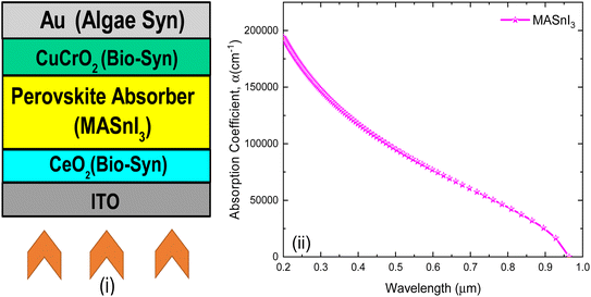 |
| | Fig. 2 (i) Simulated architecture of MASnI3-based PSC devices, and (ii) absorption coefficient of MASnI3 material under AM1.5G illuminance. | |
Table 1 The simulated inputs in the architecture of the PSC device20,31,32
| Parameters |
Terms |
ETL (CeO2) |
PVK (MASnI3) |
HTL (CuCrO2) |
| d (μm) |
Thickness |
0.1–0.15 |
0.1–0.9 |
0.1–0.15 |
| Eg (eV) |
Bandgap |
3.2 |
1.3 |
3.0 |
| εr |
Relative permittivity |
9 |
8.2 |
9.5 |
| χ (eV) |
Electron affinity |
4.4 |
4.1 |
2.1 |
| Nc (cm−3) |
Effective DoS at CB |
1 × 10²⁰ |
2 × 10¹⁸ |
1 × 10¹⁹ |
| Nv (cm−3) |
Effective DoS at VB |
2 × 10²¹ |
2 × 10¹⁸ |
1 × 10¹⁹ |
| μn (cm2 V−1 s−1) |
Mob. of electrons |
100 |
1.6 |
0.1 |
| μp (cm2 V−1 s−1) |
Mob. of holes |
25 |
1.6 |
2.53 |
| Da (cm−3) |
Dop. conc. of the acceptor |
0 |
0 |
6.4 × 10¹⁵ |
| Dd (cm−3) |
Dop. conc. of donor |
1 × 10²¹ |
1 × 10¹⁹ |
0 |
| Nt (cm−3) |
Defect density |
1 × 10¹⁴ |
1 × 10¹⁴ |
1 × 10¹⁴ |
3. Mathematical modeling
The Solar Cell Capacitance Simulator, SCAPS-1D, allows for numerical modelling of the key parameters influencing the output of a PSC device.27 Considering steady-state conditions, the semiconductor materials are governed by a one-dimensional equation. The charge density of the p–n junction, and its relationship with the electric field (E), can be depicted using the following symbols:| |
 | (1) |
Here φ is electrostatic potential; q is charge; εs is static relative permittivity for the medium; n and p are electron and hole, respectively; ND and NA are donor and acceptor densities; and Ndef is defect density for the acceptor and donor.
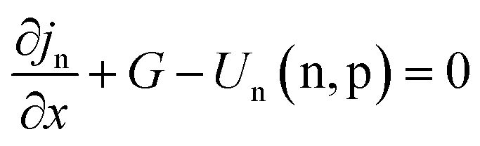
In the PSC device, the equation for carrier continuity was followed:34
| |
 | (2) |
| |
 | (3) |
where
jp and
jn are the current densities of the hole and electron;
G is the carrier generation rate; and
Un(n, p) is the recombination rate pertinent to the electron and hole.
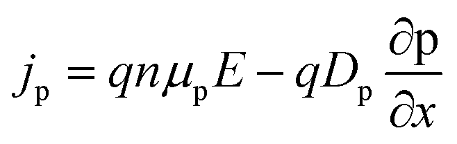
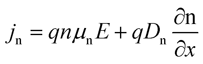
Simultaneously, the carrier current density was ascertained from the equations:35
| |
 | (4) |
| |
 | (5) |
Here
q is charge;
μp and
μn are carrier mobilities; and
Dp Dn are the diffusion coefficients of the carriers.
The basic equation pertaining to solar cells (current density, generation and recombination rate) was extracted from the SCAPS-1D software.
4. Results and discussion
An extensive examination together with an analysis pertaining to intrinsic solar cell parameters is presented in subsections 4.1 to 4.9.
4.1 Alignment of the bandgaps of the PSC structure
The band diagram encompassing the simulated device (PSC) at equilibrium is presented in Fig. 3 to understand the carrier dynamics within the device. The first MASnI3-constructed PSC device presents an energy barrier (0.02 eV) between the TiO2 conduction band minimum (EC) and the lowest unoccupied molecular orbital (LUMO) in the absorber material with an offset of around 1.85 eV between the HOMO and HTL. For an MASnI3-constructed PSC, rapid electron transport can be shown; see below. The details are depicted in Fig. 3 with ETL, HTL, and perovskite thickness.
 |
| | Fig. 3 The energy band diagrams ascribed to an MASnI3-based PSC device with designed ETL and HTL. | |
4.2 The impact of active layer thickness, ETL and HTL on PSC output
A predetermined extension applying to the preconditioned input parameters at 300 K was applied to complete the thorough simulation analysis (Table 1). Further, to understand the performance of the device with variation in absorber layer thickness, the PV parameters were obtained and are reported in Fig. 4. The effect associated with active layer thickness with reference to the output attributes of the MASnI3-based PSCs has been confirmed in Fig. 4. As the thickness of the perovskite absorbing layer (PAL) in the device grows, the short circuit current density (JSC), open circuit voltage (VOC), and power conversion efficiency (PCE%) rise to achieve a saturated value (31.31 mA cm−2) at 0.9 μm (Fig. 4). It should be highlighted that a rise in the generation rate of excitons occurred with greater absorbance in the absorber layers with PAL thickness of 0.9 μm. Additionally, the FF of the device falls monotonically as the thickness increases because a small increase in thickness increases carrier recombination.
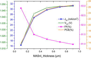 |
| | Fig. 4 The effect of the thickness of the MASnI3 layer on the PV parameters of the designed PSC device. | |
The JSC, VOC, FF and PCE at different thicknesses of CuCrO2 and CeO2 are presented in Fig. 5 and 6, respectively, to understand the impact of variation in HTL and ETL layer thickness. The parameters achieved a maximum value with thicknesses of 100 nm each of CuCrO2 and CeO2. Previous work by Bhattarai et al. also shows that the optimized ETL and HTL thickness is 100 nm.36 It achieves larger values for JSC (31.31 mA cm−2), VOC (∼1.05 V), FF (80.98%) and PCE (26.60%). This might be because of the lack of contribution to photon absorption in a PSC.22
 |
| | Fig. 5 The effect of the thickness of the CuCrO2 layer on the PV parameters of the designed PSC device. | |
 |
| | Fig. 6 The effect of the thickness of the CeO2 layer on the PV parameters of the designed PSC device. | |
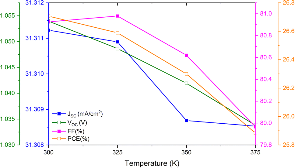
4.3 The impact of temperature on PSC parameters
A complete analysis pertaining to solar cell properties with variation in temperature is presented in Fig. 7. The four parameters, JSC, VOC, FF, and PCE, all drop as the temperature rises from 300 to 375 K, relating to the degradation of the materials. For the MASnI3-based PSC devices, JSC was a maximum at 300 K (31.31 mA cm−2). These values may be appropriate for the device output characteristics. Due to internal degradation of the PVK material, VOC continues to degrade and exhibits a higher value at 300 K (1.05 at 300 K dropping to 1.034 V at 375 K). Similarly, FF value decrease from 80.5% to 79.55% as the temperature increases from 300 K to 375 K. The PCE (26.65% at 300 K) degrades to 25.9% at a temperature of 375 K.
 |
| | Fig. 7 The effect of temperature on the solar cell PV output parameters in the PSC. | |
4.4 The impact of defect density and thickness on the parameters of the PSC
The previous subsection concerning the thickness of the fixed absorber layer with reference to the PSC device looked solely into the effects of bulk defect density on performance metrics, as reported in Fig. 8. However, varied fault concentrations at disparate thicknesses of absorber layers help us to comprehend device performance with reference to the combined variations in defect and thickness. Therefore, the collective variation is obtained in a separate subsection. Determining the impact of defect density on PSC performance as a whole is the foremost goal of a study on defect density. Initially, defect density was raised to 1 × 1016 cm−3 from 1 × 1014 cm−3 by changing the absorber layer thickness (0.1–0.9 μm). In an earlier report by Mahmoud et al. the efficiency improved with a defect density of 1 × 1014 cm−3.37 While an experimental verification by Noel et al. also depicted the same defect density in an MASnI3-based PSC.38
 |
| | Fig. 8 The contour diagrams of simulated MASnI3-PSC under optimized conditions with illuminance of AM1.5G. | |
4.5 The impact of acceptor density on the PSC parameters
The acceptor defect density varied between 1 × 1014 cm−3 and 5 × 1017 cm−3 and the corresponding PV parameters were obtained, as reported in Fig. 9. The disparity in the JSC is well observed and achieves a maximum of 31.31 mA cm−2 at 1 × 1015 cm−3 and decreases to 29.8 mA cm−2. In comparison, the VOC and FF rise as the acceptor density increases. However, the PSC-device's relevant PCE was almost equal as the acceptor defect density varied from 1 × 10¹⁴ to 5 × 1017 cm−3. So, the maximum PCE of 26.60% is presented at a smaller acceptor density (Fig. 9).
 |
| | Fig. 9 The impact of MASnI3 acceptor density on the PSC under illuminance of AM1.5G. | |
4.6 The influence of total defect density on four output parameters of the PSC
The most dominant solar cell output metrics (JSC, VOC, FF, and PCE) are presented in Fig. 10 as a function of defect density appertaining to the respective perovskite materials. Primarily, the PSC characteristics decrease as the defect density intensifies. It is crucial to note that the PSCs have drastically disparate solar cell parameter values. The MASnI3-based perovskite efficiency is 26.60% at a defect density of 1 × 1014 cm−3. The present result offers better outputs than the previous report by Dureja et al.39 The MASnI3-based PVK offers a high value of VOC, i.e. almost 1.05 V. In addition, the architecture relevant to the device exhibits the same characteristics in terms of FF.
 |
| | Fig. 10 The effect of MASnI3 defect density on the PV outputs of the PSC devices. | |
4.7 The impact of interface defect density on the output parameters of the PSCs
The study includes an investigation of CuCrO2/MASnI3 interface defect density. Fig. 11(i) shows the PCE over the defect density (Nt) pertaining to this interface. The calculation is concerned with the Fermi level relating to the device (EF). As the PCE rises at smaller values of Nt (1 × 1010 cm−2), the PCE is 26.60%. For further evaluation, the defect range from 1 × 1010 cm−2 to 1 × 1015 cm−2 was considered for further analysis. It was found that all four parameters are smaller for higher interface defect density (Nt = 1 × 1010 cm−2). The MASnI3/CeO2 interface provides valuable information about the interface defect density between the PAL and the ETL layer, as depicted in Fig. 11(ii). Numerically, the maximum value of PCE is 26.60%, drastically dropping to 17.50% at Nt = 1 × 1015 cm−2. It is emphasized that PCE is significantly affected, attributed to the higher level of Nt near the deep defect trap state.
 |
| | Fig. 11 (i and ii) The impact of both interfaces (L1 – CuCrO2/MASnI3 and L2 – MASnI3/CeO2) on the overall output of the PSC device. | |
4.8 The J–V characteristics of PSCs of different thicknesses, defect densities and temperatures
The J–V parameters pertaining to PSC devices for different ranges of thickness (100 nm to 900 nm), bulk defect density (1 × 10¹⁴ to 1 × 1016 cm−3), and temperature (300–375 K) are depicted for a simulated PSC [Fig. 12(i–iii)]. Firstly, the current density intensifies as the thickness increases to attain a saturated value of 0.9 μm [Fig. 12(i)]. This may be due to extensive higher absorption with greater thickness. In Fig. 12(ii), increasing the defects greatly impacts the voltage and lowers the voltage when it achieves a value of 0.92 V at a higher defect density value. A comparable trend was noted for raising the temperature from 300 to 375 K, as depicted in Fig. 12(iii). The higher temperature lowers the VOC, related to the damage done to the interior material of the PSC devices.31,40 The MASnI3-based PSC explicitly gives 1.05 V and 1.06 V at 300 and 375 K, respectively. The shift in potential from a higher to a lower value is well observed (Fig. 12).
 |
| | Fig. 12 Impact of (i) thickness, (ii) defect density, and (iii) temperature on the J–V parameter of the PSC devices. | |
4.9 The impedance, capacitance and EQE analysis of the optimized device
In the Nyquist curve, the X-axis represents resistance due to recombination, and the Y-axis represents the geometrical capacitance of the solar cell, indicating that the carrier accumulates at the interface layers. At high frequencies, the measured resistance resembles the recombination resistance of the material. The capacitance at high frequencies represents the geometric capacitance, signifying interface charge accumulation.41 The low-frequency response is more dubious and is related to ionic motion and hysteresis.42 It may turn into an inductive element due to the accumulation of ions and the reduction in extraction barriers. The study of imaginary and real impedance values can be well observed in Fig. 13. The impedance and real impedance show how reliable the device is, as a lower impedance is always preferable in PSC device manufacturing. The overall impedance value is −1.75 × 10⁵ Ohm cm2 with real impedance of 32![[thin space (1/6-em)]](https://www.rsc.org/images/entities/char_2009.gif) 000 Ohm cm2. Comparatively, the present work matches the value reported earlier by Bhattarai et al.43
000 Ohm cm2. Comparatively, the present work matches the value reported earlier by Bhattarai et al.43
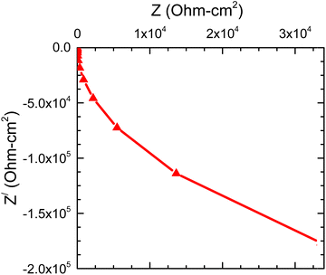 |
| | Fig. 13 Nyquist curve for the impedance analysis in the designed PSC device after all-round optimization techniques. | |
A capacitance analysis for the PSC device provides an important outlook on the designed device. It can be seen that the highest capacitance value is attained at a minimal level of defect density. The CF plot demonstrates that when the frequency surpasses 1 MHz, the capacitance reduces and saturates at a lower value. This behaviour could be attributed to specific physical processes occurring at different frequencies. The relatively smaller value of capacitance drops from nearly 8.6935 nF to 8.6915 nF in the frequency range of 106 Hertz, as depicted in Fig. 14. The capacitance of algal green-synthesized Au is much higher than the earlier reports from Bhattarai et al. for an MASnI3-based PSC.6
 |
| | Fig. 14 Capacitance analysis of the designed PSC device after all-round optimization techniques. | |
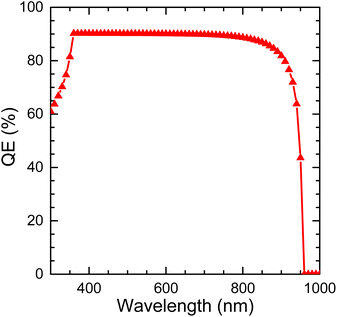
For PSCs created with MASnI3, the variation in QE with incident photon wavelength is presented in Fig. 15. The absorption of the perovskite materials can be understood with the help of the QE parameter of the PSC. The bandgap involving the absorbing layer presents an inverse relation with the QE pertinent to solar cells. The device absorbs wavelengths at varied ranges since MASnI3 has a narrow bandgap (Fig. 15). Comparatively, the current relevant simulation of an MASnI3-based PSC achieves an average QE of 90%, which is reasonably more optimised than the report mentioned above by Bhattarai et al.31 Apart from that, a detailed comparison with earlier works is given in Table 2.
 |
| | Fig. 15 Quantum efficiency (QE) with wavelength (nm) of the designed PSC device after all-round optimization techniques. | |
Table 2 A comparison of the PV parameters of the simulated device with earlier work
| Device structures |
JSC (mA cm−2) |
VOC (V) |
FF (%) |
PCE (%) |
| PSC device (present work) |
31.31 |
1.05 |
80.98 |
26.60 |
| Du et al.44 |
23.36 |
0.92 |
79.99 |
23.36 |
| Singh et al.45 |
25.75 |
1.00 |
79.21 |
20.58 |
| Alipour et al.46 |
24.65 |
1.12 |
86.02 |
23.69 |
5. Conclusions
In conclusion, the most critical solar cell attributes were analysed using the carrier transport approach in the green-synthesized carrier transport layer with reference to MASnI3-based PSC devices, and the most critical solar cell attributes were analysed. The electric parameter is predicted to be significantly more affected by the active layer appertaining to the PSC designs than by the carrier transport layers (CTLs). Therefore, PAL has been optimized for the simulated device. We obtained an appropriate active layer thickness (0.9 μm) for an MASnI3-based PSC. The green-synthesized HTL and ETL, CuCrO2 and CeO2, also improved the efficiency of the PSC device. Additionally, algae-synthesized Au nanoparticles are used as the back contact, notably being very productive so far as the cost and the overall development of the device are concerned. The capacitance and impedance analysis (imaginary vs. real Z) were also performed for the device architectures appertaining to the doping conditions to assess the dependence of the PSC device on the MASnI3 materials. The optimized PSC device achieves an excellent PCE of 26.60% for device fabrication. The study also provides a critical recommendation as well as a demonstration to help in the effective manufacturing of an MASnI3-based PSC.
Conflicts of interest
There are no conflicts to declare.
Acknowledgements
The authors would like to express their sincere gratitude to Dr Marc Burgelman and his staff at the University of Gent Belgium for providing the open-source SCAPS-1D simulation software.
References
- H. J. Snaith, Perovskites: The Emergence of a New Era for Low-Cost, High-Efficiency Solar Cells, J. Phys. Chem. Lett., 2013, 4(21), 3623–3630 CrossRef CAS.
- H.-S. Kim, S. H. Im and N.-G. Park, Organolead Halide Perovskite: New Horizons in Solar Cell Research, J. Phys. Chem. C, 2014, 118(11), 5615–5625 CrossRef CAS.
- J. M. Ball, et al., Optical properties and limiting photocurrent of thin-film perovskite solar cells, Energy Environ. Sci., 2015, 8(2), 602–609 RSC.
- S. Rhee, K. An and K.-T. Kang, Recent Advances and Challenges in Halide Perovskite Crystals in Optoelectronic Devices from Solar Cells to Other Applications, Crystals, 2021, 11 DOI:10.3390/cryst11010039.
- M. I. H. Ansari, A. Qurashi and M. K. Nazeeruddin, Frontiers, opportunities, and challenges in perovskite solar cells: A critical review, J. Photochem. Photobiol., C, 2018, 35, 1–24 CrossRef CAS.
- S. Bhattarai, et al., Performance improvement approach of all inorganic perovskite solar cell with numerical simulation, Mater. Today Commun., 2022, 33, 104364 CrossRef CAS.
- S. Bhattarai, et al., Numerical Simulation to Design an Efficient Perovskite Solar Cell Through Triple-Graded Approach, J. Electron. Mater., 2021, 50(12), 6756–6765 CrossRef CAS.
- S. Bhattarai, et al., Numerical simulation study for efficiency enhancement of doubly graded perovskite solar cell, Opt. Mater., 2021, 118, 111285 CrossRef CAS.
- A. Kojima, et al., Organometal Halide Perovskites as Visible-Light Sensitizers for Photovoltaic Cells, J. Am. Chem. Soc., 2009, 131(17), 6050–6051 CrossRef CAS PubMed.
- M. K. Hossain, et al., Numerical Analysis in DFT and SCAPS-1D on the Influence of Different Charge Transport Layers of CsPbBr3 Perovskite Solar Cells, Energy Fuels, 2023, 37(8), 6078–6098 CrossRef CAS.
- B. Rivkin, et al., Effect of Ion Migration-Induced Electrode Degradation on the Operational Stability of Perovskite Solar Cells, ACS Omega, 2018, 3(8), 10042–10047 CrossRef CAS PubMed.
- K. Kranthiraja, et al., Stability and degradation in triple cation and methyl ammonium lead iodide perovskite solar cells mediated via Au and Ag electrodes, Sci. Rep., 2022, 12(1), 18574 CrossRef CAS PubMed.
- D. Wei, et al., Photo-induced degradation of lead halide perovskite solar cells caused by the hole transport layer/metal electrode interface, J. Mater. Chem. A, 2016, 4(5), 1991–1998 RSC.
- H.-S. Kim, et al., Lead Iodide Perovskite Sensitized All-Solid-State Submicron Thin Film Mesoscopic Solar Cell with Efficiency Exceeding 9%, Sci. Rep., 2012, 2(1), 591 CrossRef PubMed.
- D. Liu and T. L. Kelly, Perovskite solar cells with a planar heterojunction structure prepared using room-temperature solution processing techniques, Nat. Photonics, 2014, 8(2), 133–138 CrossRef CAS.
- A. Singla, et al., Numerical Simulation of CeOx ETL based Perovskite Solar Cell: An Optimization Study for High Efficiency and Stability, in 2018 IEEE Electron Devices Kolkata Conference, EDKCON, 2018 Search PubMed.
- J. Chen, et al., Effect of bidentate and tridentate additives on the photovoltaic performance and stability of perovskite solar cells, J. Mater. Chem. A, 2019, 7(9), 4977–4987 RSC.
- D. Muchahary, et al., Heterojunction between crystalline silicon and nanocomposite coupled ZnO·SnO2 and optimization of its photovoltaic performance, Curr. Appl. Phys., 2022, 38, 15–21 CrossRef.
- A. Butt, et al., Biogenic synthesis of cerium oxide nanoparticles using petals of Cassia glauca and evaluation of antimicrobial, enzyme inhibition, antioxidant, and nanozyme activities, Biochem. Syst. Ecol., 2022, 104, 104462 CrossRef CAS.
- D. Sarkar, A comprehensive study on RbGeI3 Based Inorganic Perovskite Solar Cell Using Green Synthesized CuCrO2 as hole conductor, J. Photochem. Photobiol., A, 2023, 439, 1146231 CrossRef.
- B. Sharma, et al., Biosynthesis of gold nanoparticles using a freshwater green alga, Prasiola crispa, Mater. Lett., 2014, 116, 94–97 CrossRef CAS.
- A. Hima, et al., An optimized perovskite solar cell designs for high conversion efficiency, Superlattices Microstruct., 2019, 129, 240–246 CrossRef CAS.
- C. Devi and R. Mehra, Device simulation of lead-free MASnI3 solar cell with CuSbS2 (copper antimony sulfide), J. Mater. Sci., 2019, 54(7), 5615–5624 CrossRef CAS.
- S. Rawat, R. Gupta and S. Gohri, Performance assessment of CIGS solar cell with different CIGS grading profile, Mater. Today: Proc., 2023 DOI:10.1016/j.matpr.2023.03.356.
- S. Bhattarai, et
al., Numerical investigation of toxic free perovskite solar cells for achieving high efficiency, Mater. Today Commun., 2023, 35, 105893 CrossRef CAS.
- S. Bhattarai, Numerical simulation study for efficiency enhancement of doubly graded perovskite solar cell, Opt. Mater., 2021, 118, 111285 CrossRef CAS.
- M. Burgelman, et al., Modeling thin-film PV devices, Prog. Photovoltaics, 2004, 12, 143–153 CAS.
- M. Burgelman and J. Marlein, Analysis of graded band gap solar cells with SCAPS, Proceedings of the 23rd European Photovoltaic Conference, 2008 Search PubMed.
- J. Madan, et al., Device simulation of 17.3% efficient lead-free all-perovskite tandem solar cell, Sol. Energy, 2020, 197, 212–221 CrossRef CAS.
- S. Abdelaziz, et al., Investigating the performance of formamidinium tin-based perovskite solar cell by SCAPS device simulation, Opt. Mater., 2020, 101, 109738 CrossRef CAS.
- S. Bhattarai, et al., Investigation of Carrier Transport Materials for Performance Assessment of Lead-Free Perovskite Solar Cells, IEEE Trans. Electron Devices, 2022, 69(6), 3217–3224 CAS.
- S. Ahmmed, et al., Performance analysis of lead-free CsBi3I10-based perovskite solar cell through the numerical calculation, Sol. Energy, 2021, 226, 54–63 CrossRef CAS.
- S. Jeong, S. Seo and H. Shin, p-Type CuCrO2 particulate films as the hole transporting layer for CH3NH3PbI3 perovskite solar cells, RSC Adv., 2018, 8(49), 27956–27962 RSC.
- S. Bhattarai, A. Sharma and T. D. Das, Factor affecting the performance of perovskite solar cell for distinct MAPI layer thickness, AIP Conf. Proc., 2020, 2269(1), 030071 CrossRef CAS.
- S. Bhattarai and T. D. Das, Optimization of carrier transport materials for the performance enhancement of the MAGeI3 based perovskite solar cell, Sol. Energy, 2021, 217, 200–207 CrossRef CAS.
- S. Bhattarai, et al., Performance analysis and optimization of all-inorganic CsPbI3-based perovskite solar cell, Indian J. Phys., 2023, 97, 2629–2637 CrossRef CAS.
- K. H. Mahmoud, et al., Comparative Analysis of Perovskite Solar Cells for Obtaining a Higher Efficiency Using a Numerical Approach, Micromachines, 2023, 14(6), 1127 CrossRef PubMed.
- N. K. Noel, et al., Lead-free organic–inorganic tin halide perovskites for photovoltaic applications, Energy Environ. Sci., 2014, 7(9), 3061–3068 RSC.
- T. Dureja, et al., Double lead-free perovskite solar cell for 19.9% conversion efficiency: a SCAPS-1D based simulation study, Mater. Today: Proc., 2022, 71, 239–242 CAS.
- A. Thakur, D. Singh and S. Kaur Gill, Numerical simulations of 26.11% efficient planar CH3NH3PbI3 perovskite n-i-p solar cell, Mater. Today: Proc., 2022, 71, 195–201 CAS.
- E. von Hauff and D. Klotz, Impedance spectroscopy for perovskite solar cells: characterisation, analysis, and diagnosis, J. Mater. Chem. C, 2022, 10(2), 742–761 RSC.
- A. Guerrero, J. Bisquert and G. Garcia-Belmonte, Impedance Spectroscopy of Metal Halide Perovskite Solar Cells from the Perspective of Equivalent Circuits, Chem. Rev., 2021, 121(23), 14430–14484 CrossRef CAS PubMed.
- S. Bhattarai, A. Sharma and T. D. Das, Efficiency enhancement of perovskite solar cell by using doubly carrier transport layers with a distinct bandgap of MAPbI3 active layer, Optik, 2020, 224, 165430 CrossRef CAS.
- H.-J. Du, W.-C. Wang and J.-Z. Zhu, Device simulation of lead-free CH3NH3SnI3 perovskite solar cells with high efficiency, Chin. Phys. B, 2016, 25(10), 108802 CrossRef.
- N. Singh, Numerical simulation of highly efficient lead-free perovskite layers for the application of all-perovskite multi-junction solar cell, Superlattices Microstruct., 2021, 149, 106750 CrossRef CAS.
- H. Alipour and A. Ghadimi, Optimization of lead-free perovskite solar cells in normal-structure with WO3 and water-free PEDOT: PSS composite for hole transport layer by SCAPS-1D simulation, Opt. Mater., 2021, 120, 111432 CrossRef CAS.
|
| This journal is © The Royal Society of Chemistry 2023 |
Click here to see how this site uses Cookies. View our privacy policy here. 
 Open Access Article
 This Open Access Article is licensed under a Creative Commons Attribution-Non Commercial 3.0 Unported Licence
 *a,
Dharitri Borahb,
Jayashree Routc,
Rahul Pandey
*a,
Dharitri Borahb,
Jayashree Routc,
Rahul Pandey