
 Open Access Article
 This Open Access Article is licensed under a
 Creative Commons Attribution 3.0 Unported Licence
Computational-fitting method for mobility extraction in GaN HEMT
Kuan-Chang Chang a,
Xibei Fenga,
Huangbai Liua,
Kai Liua,
Xinnan Lin*b and
Lei Li*a
a,
Xibei Fenga,
Huangbai Liua,
Kai Liua,
Xinnan Lin*b and
Lei Li*a
aSchool of Electronic and Computer Engineering, Peking University Shenzhen Graduate School, Shenzhen, 518055, China. E-mail: lilei@pkusz.edu.cn
bSchool of Integrated Circuits, Anhui Polytechnic University, Anhui 241060, China. E-mail: xnlin@mail.ahpu.edu.cn
First published on 7th November 2023
Abstract
The third-generation semiconductor gallium nitride (GaN) has drawn wide attention due to its high electron mobility property. However, the classical mobility calculation methods such as Hall effect and transfer length method have limitations in accurately extracting the mobility of GaN High Electron Mobility Transistor (HEMT) due to their inability to consider the resistance in non-gate region or their high fabrication costs. This work proposes an effective yet accurate computational-fitting method for extracting the mobility of GaN HEMT. The method consists of measuring the total resistance between source and drain at different gate voltages over a very small range of overdrive voltage variations, when the sum of the transconductance and capacitance of the device is regarded as constants, and fitting a unique function of the total resistance with respect to the overdrive voltage to determine the carrier mobility and the non-gate resistance. The feasibility and reliability of the method has been also verified.
Introduction
The extraction of electrical parameters is crucial for understanding the physical phenomena underlying the operation of transistors.1–3 Among these parameters, mobility and contact resistance play a critical role in assessing the performance of various transistors.4–6 The exact extraction of mobility and contact resistance can not only optimize the design and manufacturing process, improve the performance and reliability of transistors, but also provide important data for the study of the physical and electrical properties of materials, and help the research of materials science and electronic engineering.7,8 However, when dealing with different device structures, significant errors may arise when using the deformation of the classical Sachtang equation to extract these parameters, especially in the case of devices with considerable size and long distance between the gate and drain electrodes.9The extraction of carrier mobility using the Shichman–Hodges intensive model in the linear region has been a widely used and straightforward method in silicon-based MOSFETs.10,11 Although this model does not account for the effect of non-gate region resistance, it can still be applied to the source-drain parasitic resistance of very small silicon-based MOSFETs.12,13 However, Gallium nitride high electron mobility transistor (GaN HEMT) has a large non-gate region, making it impossible to ignore the effect of non-gate-down resistance. Because of the wide bandgap, high electron mobility and other excellent physical material characteristics of GaN semiconductor, GaN HEMT has become a preferred choice for power amplifiers that require high mobility.14–17 Therefore, it is crucial to accurately calculate and extract mobility to evaluate the performance of GaN HEMT.18,19 However, the mobility calculated using the Shichman–Hodges model will be affected by the large non-gate resistance and will no longer be accurate. In this case, the most straightforward solution is to calculate the contact resistance or to exclude its effect to accurately extract the mobility.
The Hall effect method and transfer length method (TLM) are two of the most common methods for evaluating contact resistance and mobility, and are also applied to calculate the carrier mobility of GaN devices. However, each of these methods has limitations in application. The Hall effect method can only be applied to the materials that has not been made into finished products, meaning that it cannot be used to measure parameters of finished devices.20–22 The TLM method is the most widely used method, which requires specific test areas with varying pitches on the wafer, and the parameters are derived from linear fitting results.23–26 However, it is susceptible to process non-uniformity and has specific design and flow requirements. Thus, these classical methods have higher process requirements and more complex calculations, resulting in lower accuracy in extracting mobility, compared to the direct extraction of contact resistance and mobility from the completed device. Therefore, the development of alternative and more accurate techniques for extracting these parameters remains an important area of research in the field of transistor characterization.
In order to find a simple and cost-effective carrier mobility extraction method, this work proposes a computational-fitting method that is based on the fundamental equation and electrical measurements that can accurately extract the mobility of the device independent of the non-gate resistance. This method can exclude the influence of non-gate resistance and is particularly useful for addressing the challenges associated with GaN HEMTs where precise mobility analysis is difficult due to high non-gate resistance. Notably, the method proposed exhibits adaptability to a variety of materials, encompassing a wide range of emerging materials. Furthermore, the reliability and stability of this method are also verified through multiple experimental designs.
Results and discussion
Silicon-based GaN-HEMTs were chosen for demonstrating and validating the proposed mobility extraction method because of their large size, particularly the large gate-drain distance, which results in excessive non-gate resistance and makes it challenging to obtain accurate mobility using traditional methods. The GaN-HEMTs were fabricated as shown in Fig. 1. The GaN single crystal with (111) orientation was grown on the Si substrate to serve as buffer layer. Subsequently, the AlGaN/AlN/i-GaN heterostructure was synthesized using the metal–organic chemical vapor deposition (MOCVD) method. The AlGaN layer was 24.5 nm thick, and the AlN layer measured approximately 0.7 nm in thickness. The cap layer was GaN (3 nm) and the gate dielectric layer was Si3N4 (35 nm). SiO2 (300 nm) was used as passivation layer to isolate each device.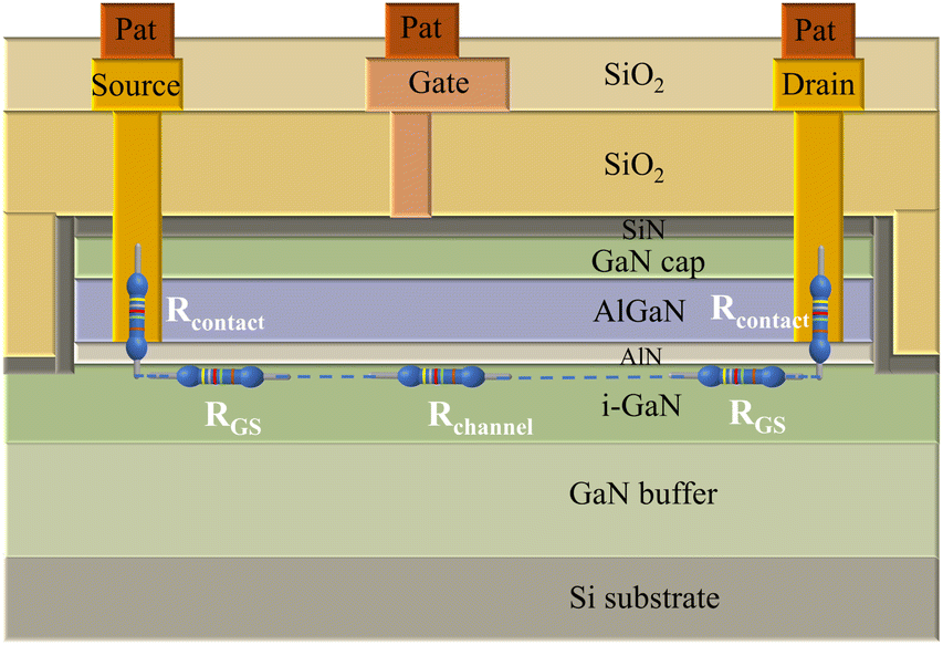 | ||
| Fig. 1 Schematic illustration of GaN-HEMTs device structure and the composition and distribution of total source–drain resistance. | ||
Fig. 2 displays the measured transfer and output characteristics, as well as stable capacitance–voltage (C–V) characteristics, which are crucial for the proposed extraction method.
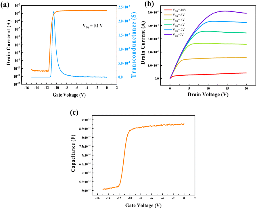 | ||
| Fig. 2 The basic electrical performance of GaN-HEMTs. (a) Transfer characteristic measured at 0.1 V drain voltage. (b) Output characteristics with gate voltage ranging from −10 V to 0 V. (c) C–V characteristics measured at the frequency of 100 kHz. | ||
The total source-drain resistance of GaN HEMT consists of the sub-gate resistance and the non-gate region resistance, which can be expressed as:
| RSD = 2Rcontact + RGS + RGD + Rchannel | (1) |
Rchannel is the channel resistance under the gate, which is controlled by the gate voltage. Rcontact is the contact resistance. RGS is the resistance between gate and source. RGD is the resistance between gate and drain. These resistances have constant magnitudes under DC stability and can therefore be treated as constants, which can be expressed as:
| Rconstant = 2Rcontact + RGS + RGD | (2) |
Therefore, the influence of Rcontact, RGS, RGD can be excluded by treating them as a constant Rconstant. As a result, the total resistance between source and drain can be expressed as
| RSD = Rconstant + Rchannel | (3) |
The basic current equation could be expressed as
| ΔI = ΔQμE | (4) |
| ΔQ = CoxΔVGS | (5) |
| ΔI = gmΔVGs | (6) |
The current equation could be transformed into
 | (7) |
 | (8) |
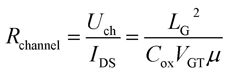
The final result could be brought out by bring Formula (6) back to Formula (1)
 | (9) |
A linear relationship was established between RSD and μ, where RSD could be directly obtained from the measurement results. The mobility and non-gate resistance could be calculated from the slope and intercept, respectively.
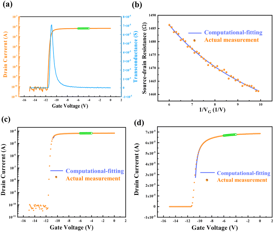
Fig. 3 illustrates in detail the computational-fitting method and the corresponding results. Initially, the transfer characteristics were measured at VD = 0.1 V, and VG ranging from −15 V to 0 V in 0.1 V increments, yielding a stable ID and a corresponding gate voltage range. Then RSD was measured based on the above-obtained VG range, where VGS changes from −6 V to −4 V with 0.1 V increments, and VD ranges from 0 to 0.3 V to ensure the quasi-static conditions, allowing carrier mobility and electrical field in channel to be approximately constant.26 The final fitting results demonstrate that this HEMT device has a mobility of approximately 302.3 cm2 V−1 s−1, and a non-gate resistance of 1531 Ω.
 | ||
| Fig. 3 The fitting process of mobility and non-gate resistance. (a) Transfer characteristics measured at VD = 0.1 V, (b) ID measured at a small range of VD. (c) RSD measured with gate voltage ranges from −6 V to −4 V. (d) A comparison of RSD between fitting and measured results. | ||
Fig. 3 illustrates in detail the computational-fitting method and the corresponding results. Initially, the transfer characteristics were measured at VD = 0.1 V, and VG ranging from −15 V to 0 V in 0.1 V increments, yielding a stable ID and a corresponding gate voltage range. Then RSD was measured based on the above-obtained VG range, where VGS changes from −6 V to −4 V with 0.1 V increments, and VD ranges from 0 to 0.3 V to ensure the quasi-static conditions, allowing carrier mobility and electrical field in channel to be approximately constant.27 The final fitting results demonstrate that this HEMT device has a mobility of approximately 302.3 cm2 V−1 s−1, and a non-gate resistance of 1531 Ω.
A series of experiments were conducted to verify the feasibility and stability of the computational-fitting approach. The device mobility and non-gate resistance were calculated by fitting within the Vg range of −6 V to −4 V. The resulting values were then substituted into the fitted model (eqn (9)) to derive the electrical characteristics of the entire device. This allows for the derivation of the electrical characteristics of the device outside of this measurement range (i.e., VG outside of −6–−4 V) based on the calculated values. The transfer characteristic curve of the HEMT device back-propagated by this method is depicted in Fig. 4. The fitting characteristic curve shows high consistence with the actual measured result of the HEMT device, demonstrating that the computational-fitting method is reliable and also an effective method for accurately determining the electrical characteristics of HEMT devices beyond the measurement range.
 | ||
| Fig. 4 The feasibility of computational-fitting method. (a) and (b) show the computation and fitting process, in which mobility and non-gate resistance were obtained. (c) and (d) show the electrical characteristics in logarithmic and linear coordinates, respectively, which were reversely derived from the computational-fitting method to verify the accuracy. | ||
Moreover, to ensure the robustness of the computational-fitting approach, 50 sets of carrier mobilities and non-gate resistances were extracted from the same HEMT device using the fitting method for 50 times, as shown in Fig. 5. The resulting 50 sets of mobility data exhibited a small standard deviation of 6.1 cm2 V−1 s−1 and a mean value is 336.2 cm2 V−1 s−1, with a concentrated data distribution and a fluctuation of only 1.8%. Similarly, the 50 sets of non-gate resistance data had a small standard deviation of 3.7 Ω and a mean value of 1521 Ω, with a fluctuation of only 0.3%. These results demonstrate that there is no correlation between the measurement series and the fitting results, validating the stability of the computational-fitting approach. Furthermore, 50 HEMT devices have been tested to evaluate robustness when accounting for device-to-device variation. The mean values for mobility and non-gate resistance are 301.6 cm2 V−1 s−1 and 1365.6 Ω, respectively. The standard deviation (sigma) for mobility and non-gate resistance stands at 7.1 cm2 V−1 s−1 and 4.9 Ω, exhibiting a mere 2.3% and 0.4% fluctuation, underlining the exceptional robustness of this method in accommodating device-to-device variations. Therefore, this method is reliable and can be applied to accurately determine the carrier mobilities and non-gate resistances of HEMT device.
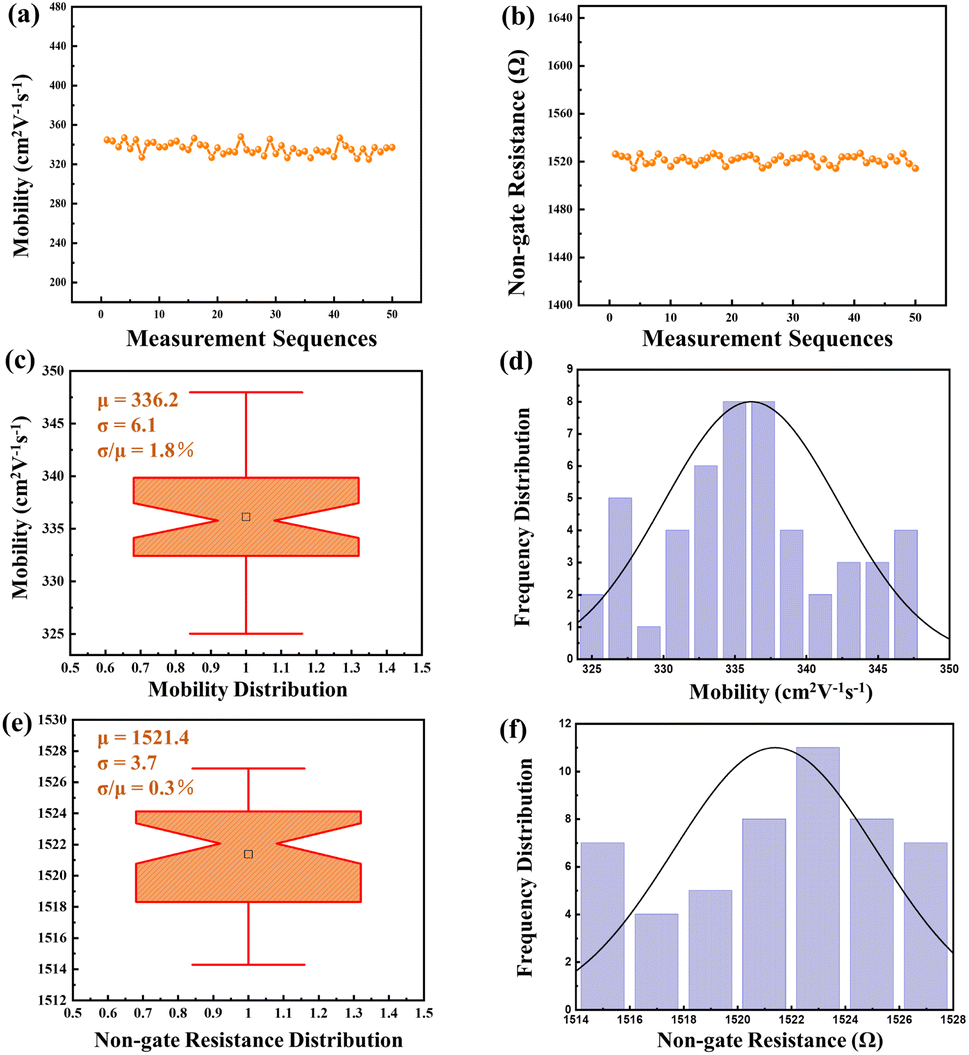 | ||
| Fig. 5 The reliability of computational-fitting method. (a) and (b) show the measurement results of mobility and non-gate resistance for 50 times. (c) and (e) show the distribution of mobility and non-gate resistance respectively using box plots. (d) and (f) show the normal distribution of mobility and non-gate resistance respectively. | ||
Conclusions
In summary, this work demonstrated an effective method for extracting carrier mobility from GaN HEMT device using a computational-fitting technique based on the fundamental current equation and actual electrical measurements. The proposed method achieves high accuracy, simplicity, and low cost compared to traditional methods. It is particularly useful in cases where the non-gate region is quite large and the effect of non-gate resistance cannot be ignored. The proposed computational-fitting method has also been verified to exhibit excellent reliability and stability without any negative impact on the calculation of GaN HEMT mobility. Therefore, it is a valuable method for accurately determining carrier mobility in such devices. Overall, this work presents a significant contribution to the field of GaN HEMT device characterization and provides a valuable tool for future research in this area.Author contributions
Kuan-Chang Chang: investigation, formal analysis, writing – original draft, writing – review & editing. Xibei Feng: data curation, validation, writing – review & editing. Huangbai Liu: data curation, visualization. Kai Liu: validation. Xinnan Lin: resources, project administration. Lei Li: conceptualization, methodology, writing – review & editing, funding acquisition.Conflicts of interest
There are no conflicts to declare.Acknowledgements
This study was supported by the National Natural Science Foundation of China (No.: 62074007, No.: 62204007), the Shenzhen Municipal Scientific Program (no. JCYJ20220531093210023, JCYJ20200109140610435), the Shenzhen Fundamental Research Program (no. GXWD20201231165807007-20200814122231001) and the Start-up funding of Anhui Polytechnic University.References
- Y. Qin, Y. Xiao and L.-D. Zhao, APL Mater., 2020, 8, 010901 CrossRef CAS.
- G. J. Snyder, A. H. Snyder, M. Wood, R. Gurunathan, B. H. Snyder and C. Niu, Adv. Mater., 2020, 32, 2001537 CrossRef CAS PubMed.
- Y. Xiao, H. Wu, J. Cui, D. Wang, L. Fu, Y. Zhang, Y. Chen, J. He, S. J. Pennycook and L.-D. Zhao, Energy Environ. Sci., 2018, 11, 2486–2495 RSC.
- Y. Xiao and L.-D. Zhao, npj Quantum Mater., 2018, 3, 55 CrossRef.
- P.-C. Liu, C.-H. Chang and C.-S. Fuh, RSC Adv., 2016, 6, 106374–106379 RSC.
- P.-T. Liu, C.-H. Chang and C.-J. Chang, Appl. Phys. Lett., 2016, 108, 261603 CrossRef.
- Y.-C. Cheng, S.-P. Chang, C.-P. Yang and S.-J. Chang, Appl. Phys. Lett., 2019, 114, 192102 CrossRef.
- K. Liang, D. Li, H. Ren, M. Zhao, H. Wang, M. Ding, G. Xu, X. Zhao, S. Long, S. Zhu, P. Sheng, W. Li, X. Lin and B. Zhu, Nano-Micro Lett., 2021, 13, 164 CrossRef CAS PubMed.
- S. M. Sze and K. K. Ng, Physics of Semiconductor Devices, Wiley, Taiwan, 2007 Search PubMed.
- H. Shichman and D. A. Hodges, IEEE J. Solid-State Circuits, 1968, 3, 285–289 CrossRef.
- M.-H. Hsu, S.-P. Chang, S.-J. Chang, W.-T. Wu and J.-Y. Li, ECS J. Solid State Sci. Technol., 2018, 7, Q3049–Q3053 CrossRef CAS.
- G. Xu, L. Cai, Z. Wang, Q. Wu, C. Lu, Z. Zhao, Y. Zhao, D. Geng, L. Li, M. Liu and Y. Yang, IEEE Trans. Electron Devices, 2019, 66, 5166–5169 CAS.
- C. Liu, G. Li, R. Di Pietro, J. Huang, Y.-Y. Noh, X. Liu and T. Minari, Phys. Rev. Appl., 2017, 8, 034020 CrossRef.
- T. Lian, Y. Xia, Z. Wang, X. Yang, Z. Fu, X. Kong, S. Lin and S. Ma, Microsyst. Nanoeng., 2022, 8, 119 CrossRef CAS PubMed.
- P. Cui and Y. Zeng, Sci. Rep., 2022, 12, 16683 CrossRef CAS PubMed.
- K. J. Chen, O. Haberlen, A. Lidow, C. L. Tsai, T. Ueda, Y. Uemoto and Y. Wu, IEEE Trans. Electron Devices, 2017, 64, 779–795 CAS.
- P. Cui, A. Mercante, G. Lin, J. Zhang, P. Yao, D. W. Prather and Y. Zeng, Appl. Phys. Express, 2019, 12, 104001 CrossRef CAS.
- I. Nifa, C. Leroux, A. Torres, M. Charles, G. Reimbold, G. Ghibaudo and E. Bano, Microelectron. Eng., 2019, 215, 110976 CrossRef.
- C. Mizue, Y. Hori, M. Miczek and T. Hashizume, Jpn. J. Appl. Phys., 2011, 50, 021001 CrossRef.
- D. A. Bandurin, A. V. Tyurnina, G. L. Yu, A. Mishchenko, V. Zolyomi, S. V. Morozov, R. K. Kumar, R. V. Gorbachev, Z. R. Kudrynskyi, S. Pezzini, Z. D. Kovalyuk, U. Zeitler, K. S. Novoselov, A. Patane, L. Eaves, I. V. Grigorieva, V. I. Fal'ko, A. K. Geim and Y. Cao, Nat. Nanotechnol., 2017, 12, 223–227 CrossRef CAS PubMed.
- S. Nakamura, Jpn. J. Appl. Phys., 1991, 30, L1705–L1707 CrossRef.
- S. Ponce, D. Jena and F. Giustino, Phys. Rev. Lett., 2019, 123, 096602 CrossRef CAS PubMed.
- Z. Zheng, W. Song, L. Zhang, S. Yang, J. Wei and K. Chen, IEEE Electron Device Lett., 2020, 41, 26–29 Search PubMed.
- H. Jiang, C. Liu, Y. Chen, X. Lu, C. W. Tang and K. M. Lau, IEEE Trans. Electron Devices, 2017, 64, 832–839 CAS.
- C. Sharma, R. Singh, D.-S. Chao and T.-L. Wu, J. Electron. Mater., 2020, 49, 6789–6797 CrossRef CAS.
- X. Li, M. Van Hove, M. Zhao, K. Geens, V.-P. Lempinen, J. Sormunen, G. Groeseneken and S. Decoutere, IEEE Electron Device Lett., 2017, 38, 918–921 CAS.
- G. Fishman, Phys. Rev. B, 1986, 34, 2394–2401 CrossRef PubMed.
| This journal is © The Royal Society of Chemistry 2023 |