DOI:
10.1039/D3RA06430A
(Paper)
RSC Adv., 2023,
13, 30252-30263
Molecular dynamics simulation of the amorphous graphite-like membrane deposited on ideal graphite substrate
Received
21st September 2023
, Accepted 9th October 2023
First published on 16th October 2023
Abstract
To understand the growth mechanism of pyrolytic graphite on ideal graphite substrate by chemical vapor deposition (CVD), the process simulated by molecular dynamics is performed. The simulation revealed that only an amorphous graphite-like membrane (a-GLM) can be obtained using the Tersoff potential function. It is revealed that the formation process for the first layer of the a-GLM initiates from the firstly deposited carbon monomers, dimers, and trimers as growth points, on which Y-shaped long chain is formed, and then the network with pores are developed, and finally the graphene-like layer with six-membered dominated rings appears after repair treatment. The following deposition simulation for more deposited carbon atoms indicates that a second layer like-graphene is more prone to superpose onto the microdomains of the first layer like-graphene until the formation of the island-like bumps, and the concave zone around the bumps will be filled by deposited atoms and modified by defect repair. The growth mechanism for pyrolytic graphite prepared by CVD can be deduced by the simulation inspiration. The optimal deposition temperature of 2400 K is acquired by evaluating the integrity of the first deposited graphene film by statistics of five-to-seven-membered carbon ring number. This study can provide theoretical references for the design of the pyrolytic graphite production process.
1 Introduction
Pyrolytic graphite (PyG) is a polycrystal prepared by chemical vapor deposition (CVD) from hydrocarbon gas compounds at high temperatures and usually deposited on a high-density graphite substrate. PyG has controllable high orientation and anisotropy due to the tendency of the interlayer planes to grow parallel to the substrate surface.1–3 PyG has good heat resistance, thermal and electrical conductivity and stable chemical properties, and widely used in propellant rocket nozzles, gates of electronic tubes and various protective coatings for electronic devices.4–6 Microstructural studies of PyG show that PyG graphite layers are stacked often in a non-ideal ABAB stacking manner, i.e., in a disordered layer stacking in the [001] direction, and thus the general PyG graphite interlayer distance is slightly greater than the layer spacing of 3.4 Å for ideal single-crystal graphite.7 PyG preparation conditions, such as temperature and pressure of CVD pyrolysis, flow rates of carbon source gas and substrate selection, have a significant impact on the microstructure and properties of PyG, thus the preparation of high-quality anisotropic pyrolytic graphite and the study of microscopic kinetic processes have always been the focus of attention. Hareesh et al.8 prepared PyG coatings by CVD method and investigated the effect of pyrolysis temperature on the microstructure, density, oxidation kinetics, and growth and nucleation modes of the deposited PyG. It was found that the PyG growth rate was proportional to the pyrolysis temperature, the disorder of stacking was inversely proportional to the pyrolysis temperature, and the increase of temperature favors for the graphitization of PyG. While Zhu9 studied the effect of the pressure and temperature on the microstructural changes of PyG prepared by CVD method and found that the increase in pressure was favorable for PyG initial growth. Zheng10,11 investigated the effect of carbon source at different flow rates on the microstructure of carbon in carbon fiber growth pyrolysis carbon and found that the higher the flow rate, the better the growth quality.
The mature high-temperature CVD process of PyG can meet the general industrial demand.12,13 However, the microscopic process of PyG high-temperature deposition is still unclear. Experimental studies of the microscopic deposition process of PyG prepared by CVD method are extremely complicated to implement and difficult to achieve in situ observational studies at high temperatures. At present, molecular dynamics (MD) simulation has become an effective means to study the microscopic formation process of material preparation and properties.14–16 The currently reported MD studies of related graphite almost focused on exploring the growth of graphene deposited on various substrates. For example, Rasuli17 used MD methods to study the effect of depositing graphene on Ni substrates with different carbon source flow energies, different substrate temperatures, and different precursor carbon formation rates, and concluded that the high-quality graphene on Ni (100) crystal surfaces can be obtained by the optimized conditions. Zhang L.18 explored MD simulations of self-limiting growth of monolayer graphene on Cu surfaces by CVD and studied the graphene growth process in detail, such as graphene nucleation, ring formation and defect self-healing. Liu et al.19 explored the effect of methane flow rate and the content of Co in the substrate alloy on the quality of graphene deposited on cemented carbide substrate using the MD method for high-temperature methane cracking deposition, and pointed out that the graphene formation process is dominated by direct growth. Huang20 studied by MD method that the microscopic atomic-level growth process of graphite-like films sputter-deposited on silicon substrates, and the simulation studies showed that sputtering energy below 10 eV could get graphite-like films with high sp2 hybrid content, low density and high tensile stress; however, as the carbon sputtering energy gradually increased to 40 eV, the film stress changed from tensile stress to compressive stress and reached the extreme value, and the content of sp3 hybrid herein was also the highest; 50 eV carbon sputtering energy can make the roughness of the graphite-like film lowest, and the prepared graphite with high planar quality can be used as high-density magneto-optical storage devices.
In contrast, MD studies of low-temperature deposition of single-layer graphene on metallic substrates,21–25 and MD studies of high-temperature deposition of multilayer graphene structures PyG on the graphite substrates have not been reported. In this study, with reference to the MD study of low-temperature deposition of monolayer graphene on metallic substrates, we tried to use the appropriate Tersoff potential parameters and write the main program using the LAMPPS open-source package to explore the deposition process of carbon atoms of high-temperature pyrolytic graphite. This paper is expected to reveal the initial deposition growth process of PyG on natural graphitic carbon substrates and explore the effects of different CVD deposition temperatures on the initial monolayer growth as well as multilayer stacked growth of PyG.
2 Simulation method
2.1 Simulation box establishment
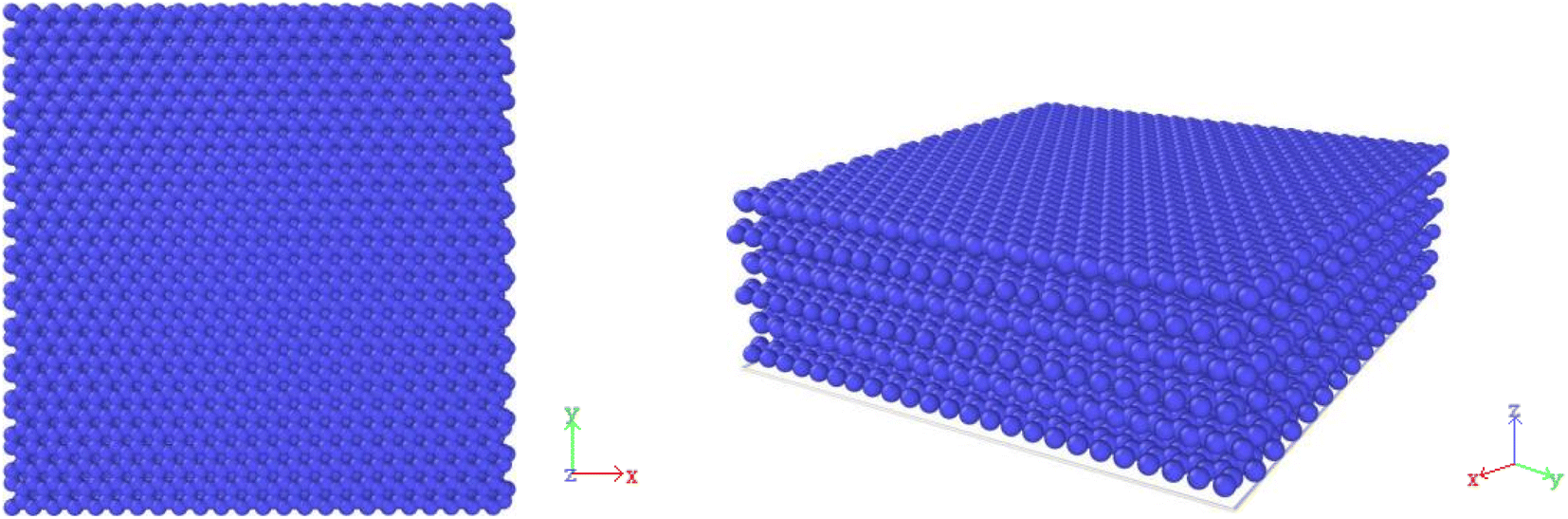
Fig. 1 shows a simple model of 59.0 × 59.0 × 65.1 Å in size by 6 layers of graphene representing an ideal graphite substrate structure with 8064 carbon atoms in the substrate, using periodic boundary conditions in X, Y directions and fixed boundary conditions in Z direction. Because the theoretical space between graphite base layers is 3.35 Å, the space between the third layer graphene of the substrate and the first deposited carbon layer is 13.6 Å, and the van der Waals forces of the lower three layers carbon atoms of the substrate to the deposited atoms are almost negligible, so the lower three layers atoms of the substrate are fixed and the role of the upper three layers of the substrate atoms are only considered. The whole system is solved by numerical integration velocity algorithm (Verlet) using canonical ensemble (NVT), and the temperature of substrate is controlled by Berendsen thermal bath method. The simulation time step is set to 1 fs, and the damping factor is 0.1 fs. The graphite substrate was heated to 300 K with full relaxation of 100 ps to bring the substrate energy close to equilibrium. Methane is used as a high-quality carbon source for the deposition and production of carbon materials such as PyG, graphene, and fullerene, the final product of methane pyrolysis is C and H2 (ref. 42–49). In the simulation box, the starting carbon source in the simulated system can be considered as the cracked carbon from CH4 carbon source, and the carbon source flux rate was characterized by the carbon atom flux rate (CDR) deposited on the substrate, which was set to 10 ps−1. The simulated temperatures were set to 1500–3000 K (interval 300 K).
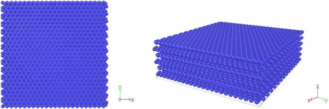 |
| | Fig. 1 Graphite substrate model composed of 6 layers of graphene in AB stacking form. | |
2.2 Potential function selection
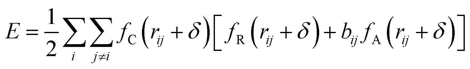
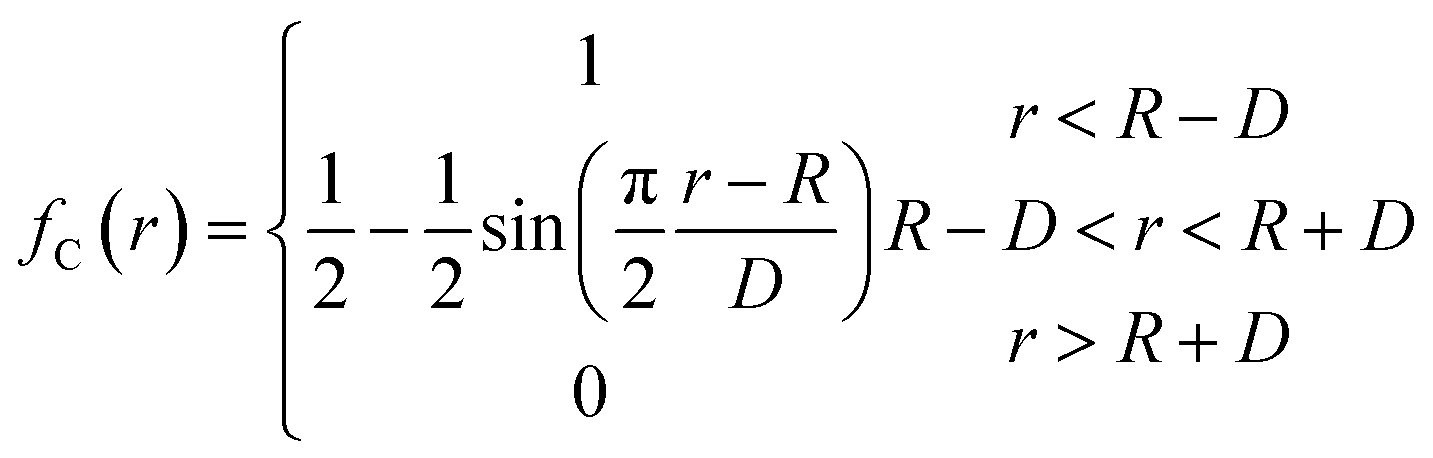
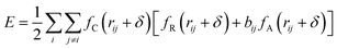
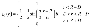
The potential function describes the interaction energy between particles with respect to their positions, and this paper deals with three configurations of carbon atoms, i.e., the solid-phase carbon atoms in graphite matrix crystalline, the amorphous carbon atoms newly deposited, and gas-phase carbon atoms. The reported simulation studies of deposited graphene mostly use the Airebo potential,26,27 which relies on the mutual bonding strength of the carbon atoms and the coupling between C–C. Airebo potential consists of three parts, namely, the short-range bonding potential, the long-range interaction potential, and the dihedral angle torsion potential, which can be accurately applied for the growth of monolayers of graphene hybridized with sp2 orbitals. Tersoff28,29 as a kind of many-body potential can also be accurately applied to the growth of graphene for the time being, which can accurately describe the covalent properties of C–C bonds, and can truly respond to behaviors of bond angles, bond lengths, bond energies, lattice constants, etc. when the bonds dynamically break or recombine. After the post-modification of the Tersoff potential function by Brenner,30 the Tersoff potential function can be more accurately applied to the depositing carbon systems.20,34,35 In this paper, the Tersoff potential function is used to describe the interactions between substrate carbon atoms, between substrate carbon atoms and deposited carbon atoms, and between deposited carbon atoms. Eqn (1) gives the specific expression for the Tersoff potential function, where E, fC, rij, δ, fR, bij, fA is denoted as the total potential energy, truncation function, distance from atom i to j, distance deviation, repulsion potential, bond order function, attraction potential, respectively; eqn (2) gives the truncation function in the simulation process, where r is the truncation distance, D, R are the parameters of the potential function, and (R − D) and (R + D) are the left and right truncation values of the truncation function. Fig. 2 gives a plot of the potential energy change of the natural graphite substrate when it is heated to 1500 K and then fully relaxed for 100 ps. The potential energy change of the natural graphite substrate is shown in Fig. 2.| |
 | (1) |
| |
 | (2) |
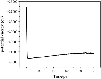 |
| | Fig. 2 Potential energy change of a natural graphite substrate relaxing at 300 K for 100 ps. | |
3 Results and discussion
3.1 Nucleation and growth of a-GLM on graphite substrates
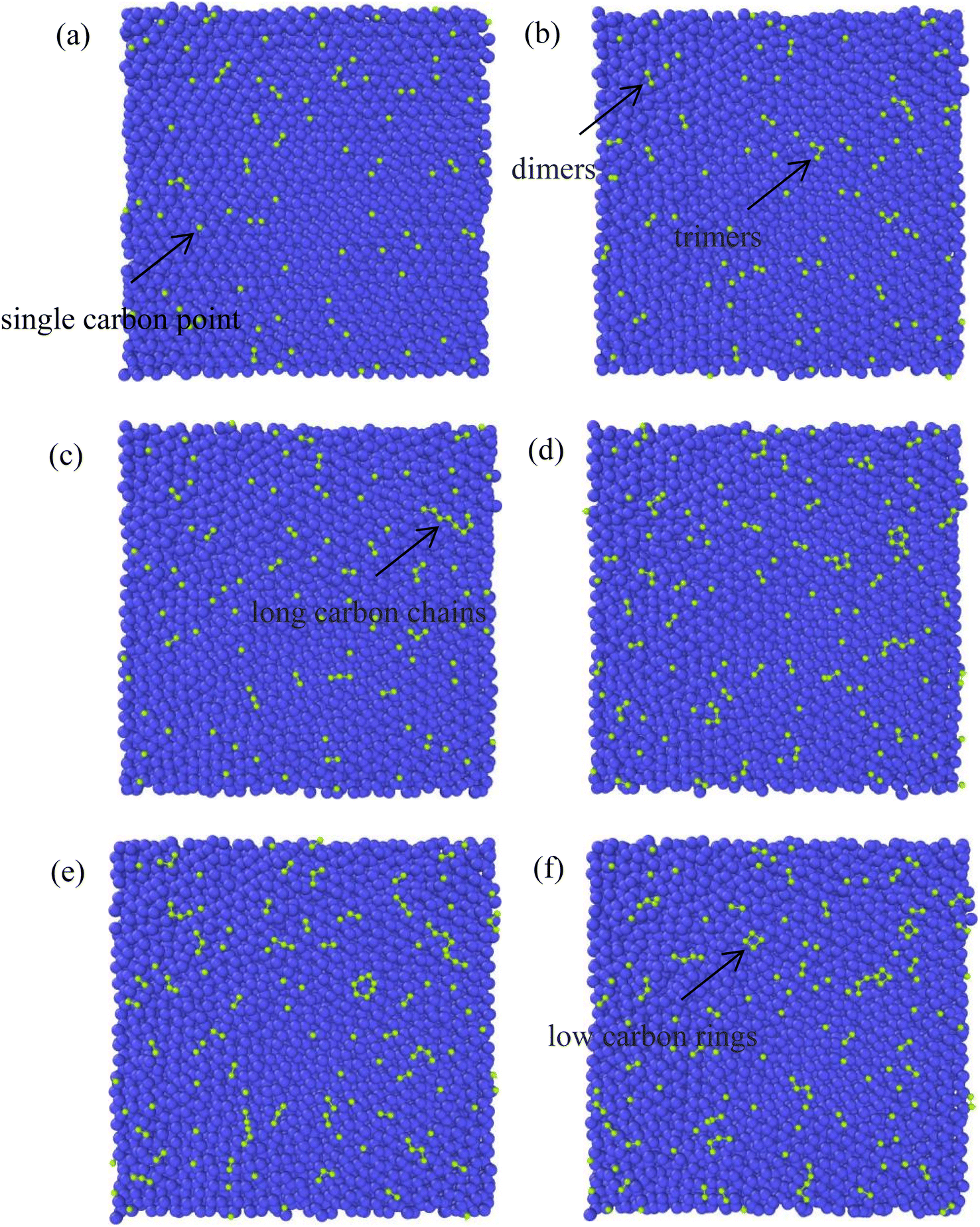
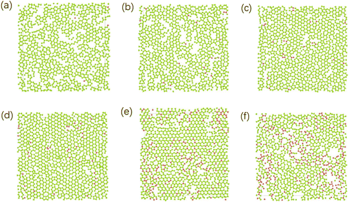
3.1.1 Effect of temperature on the initial nucleation points. The effect of temperature on the attachment ability and nucleation of pyrolitic carbon atoms on the active sites of the substrate was investigated by the formation of the first layer of graphite-like membrane deposited on an ideal graphite substrate. Fig. 3(a)–(f) represent the distribution of dispersed carbon particles initially deposited on the substrate during the deposition of 420 ps at temperatures of 1500–3000 K. At relatively low deposition temperatures of 1500 K (Fig. 3(a)) and 1800 K (Fig. 3(b)), amounts of monocarbons, dimers, trimers, and tetramers and a few polymers with polycarbon chains are dispersed on the substrate. The stable dimers and trimers can be regarded as nucleators, on which tetrameric rings or long carbon chains are developed in combination with the attraction from the substrate. At a higher temperature of 2100 K (Fig. 3(c)), the nucleation points of dimers and trimers on the substrate surface decrease, while the carbon chain grows significantly, and the deposited carbon particles are attached by the carbon chain. Most nucleation sites grow into tetramers or oligomers when the deposition temperature reaches 2400 K (Fig. 3(d)). When the temperature reaches 2700 K (Fig. 3(e)), the thermal movement of carbon atoms at so high temperature is intensified, and some of the long chain is broken and dissociated into a few carbon rings. When the deposition temperature reaches 3000 K (Fig. 3(f)), all the long chains are directly split and form some low carbon rings. Meanwhile, the deposited carbon atoms penetrate into the matrix increase, and some carbon atoms from substrate diffuse into the deposition layer.
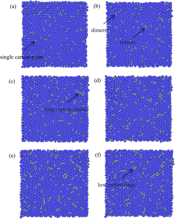 |
| | Fig. 3 The distribution of deposited carbon atoms at 1500–3000 K after 420 ps (graphite matrix in blue, deposited carbon atoms in green) (a) 1500 K; (b) 1800 K; (c) 2100 K: (d) 2400 K; (e) 2700 K; (f) 3000 K. | |
In this simulation series, it is found that in the range of deposition temperature 1500–1800 K, the nucleation points dimer and trimer on the substrate have more distribution positions, and for the deposition temperature 2100–2700 K, the number of nucleation points decreases, and the number of oligomers increases. When the deposition temperature reaches 3000 K, the surface deposited carbon atoms will be evacuated and simultaneously a large number of matrix carbon atoms will enter into the deposition layer, as a result, the substrate is destroyed, the number of deposition surface carbon atoms is decreased and the integrated membrane is hard to be formed.
3.2 Microscopic growth process of the first layer a-GLM
The growth process of the first layer a-GLM and its quality were studied at 2400 K within deposition time 1800 ps. The residual deposited carbon structures over 2 layers were truncated for easy observation. Fig. 4(a)–(i) represent the deposition and growth process of the first layer graphene-like film on graphite substrate at the simulated temperature of 2400 K, within 1800 ps, by CDR of 10 ps−1. Fig. 4(j) represents the top view of the whole deposited carbon structure untruncated. As shown in Fig. 4(a), many dispersed single carbon atoms on the graphite substrate appear at 300 ps of system deposition. As the deposition time increases, more carbon atoms impact the substrate and bond sequentially at the single carbon sites, and it can be observed that at 400 ps (see Fig. 4(b)) the dimer and trimer nucleation sites increase sequentially, and the nucleation sites begin to spread over the entire substrate. At 500 ps and 600 ps, four-membered rings (see Fig. 4(c)) and six-membered rings (see Fig. 4(d)) can be observed near the basal nucleation sites. At 600 ps, the deposition of carbon atoms in the vicinity of the nucleation points is increasing, some carbon atoms near the nucleation points tend to combine and polymerize into a long chain, other free carbons can be captured by carbon rings and extend the long chain on the rings. As shown in Fig. 4(e) and (f), at 700 ps, with chain end atoms of the long chain or branched chain continue to capture the deposited carbon atoms, the number of long chains continue to increase; with the reaction time to 800 ps, the ends of these different long chains are combined and form a large ring, which is extremely unstable and can be easily split. In Fig. 4(g), i.e., at 1000 ps, it can be observed that the hole defects in the formed macro-ring are larger, and fewer carbon atoms are deposited in the hole defects, and attracted into the ring and expanded inward. As shown in Fig. 4(h) and (i), the long carbon chains deposited have overcome the energy barriers and branch-grafted each other, and the large carbon rings with large pore defects will be filled by carbons and continue to polymerize inwardly with the increase of carbon atoms number. At 1400 ps (Fig. 4(h)), it can be significantly seen that with the large rings polymerized inwardly, they evolve into a small ring until 1800 ps (Fig. 4(i)), at this time, the network structure of a-GLM base layer almost spread over the entire substrate.
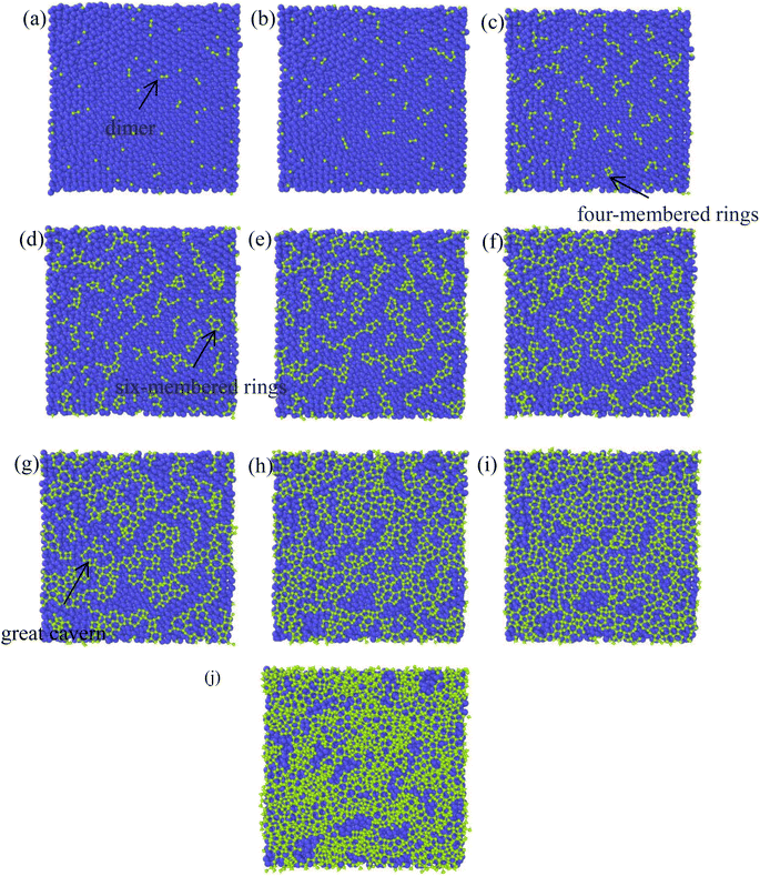 |
| | Fig. 4 Growth process of carbon deposition in graphite matrix at 2400 K (graphite matrix in blue, deposited carbon atoms in green) (a) 300 ps; (b) 400 ps; (c) 500 ps; (d) 600 ps; (e) 700 ps; (f) 800 ps; (g) 1000 ps; (h) 1400 ps; (i) 1800 ps; (j) the whole structure untruncated. | |
Throughout the deposition simulation, carbon atoms preferentially deposit on the active points of the substrate and attached monocarbon sites are formed in the initial 300 ps, and the following deposition occurs near the nucleation point more effectively. Carbon dimer, trimer and small carbon rings can be formed around the nucleation sites. With time, some nucleation sites continue to capture surrounding carbon atoms in different directions and Y-shaped long chains or dendrites of carbon polymer appear. As the reaction proceeds, the long chain structure unstable extremely splits into multiple small carbon-rings. In both Fig. 4(e) and (f), seven-membered rings and larger are observed, which split into six-membered rings and form graphene-like network. For carbon rings with larger pores, a certain number of carbon atoms will be deposited inside the defects, and the carbon atoms of carbon ring can capture the inside carbon atoms and make the defects smaller, thus turning the whole structure into a network. After 1800 ps deposition, the first layer of deposited carbon atoms covers more than 80% of the surface (Fig. 4(i)), which can be considered as the formation of the deposited graphene-like basic layer.
3.3 Temperature effect on the quality of deposited first layer a-GLM
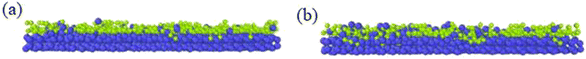
Different temperatures can result into different defects of the deposited graphite structures. Fig. 5 shows the final structure of the first layer of graphene-like mesh after 1800 ps deposition at variable temperatures of 1500–3000 K, by CDR of 10 ps−1 and after relaxation treatment at the corresponding temperatures. Fig. 6(a) and (b) represents the side views of a-GLM deposited at 2700 K and 3000 K, respectively. As shown in Fig. 5(a)–(d), the deposited graphite grid defects gradually decrease at 1500–2400 K with increasing temperature. With temperature increase further, the defects of first layer a-GLM deposited at a temperature of 2700 K (see Fig. 5(e)), more defects are shown at 3000 K (see Fig. 5(f)). Moreover, from all the pictures in Fig. 5, it can be obviously observed that the substrate carbon atoms (red color) diffused into the a-GLM gradually increase, simultaneously, the deposited atoms (blue color) also perpetrated into the substrate (see Fig. 6), especially at 3000 K. It can be seen in Fig. 6(b) that the substrate is distorted and damaged at so high temperature. This is attributed to the intensified thermal movement of all carbon atoms at higher temperatures. The larger defects of the first layer a-GLM deposited and the damage of substrate at 2700–3000 K indicate the much higher deposition temperature is not favored for preparation of graphite by CVD.
 |
| | Fig. 5 The top views of the first layer of graphite-like membrane after 1800 ps, at temperatures of 1500–3000 K (a) 1500 K; (b) 1800 K; (c) 2100 K; (d) 2400 K; (e) 2700 K; (f) 3000 K. | |
 |
| | Fig. 6 Profile diagrams of graphite-like membrane and substrate at the high temperatures after 1800 ps at (a) 2700 K and (b) 3000 K. | |
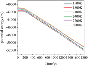
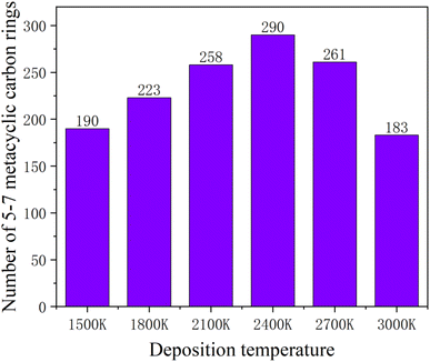
Increasing temperature can enhance the kinetic energy of carbon atoms, increase atom collision probability, and increase the growth rate; however, in this simulation system, the box is fully filled with carbon atoms of substrate in X and Y directions, so the over high temperature will lead to Z direction escape movement of a large amount of carbon atoms, and result into collapse of simulation. Fig. 7 shows the average potential energy change curve of carbon atoms deposited during the deposition process at temperatures 1500–3000 K and within 1800 ps. It can be seen that the average potential energies of the system increase with temperatures, and decrease with time. The temperature determines the kinetic energy of the deposited atoms. The appropriate temperature increase can make the carbon atoms deposited on the surface migrate faster to the neighborhood of the long chain, accelerating the formation of the complete graphite lattice. Fig. 8 represents the final numbers of carbon rings deposited at temperatures 1500–3000 K and after 1800 ps. It can be seen that a relatively perfect first graphite lattice with the maximum number of 5–7-membered carbon rings can be obtained at a temperature of 2400 K. In the simulation, the optimal deposition temperature of the deposited graphite films with best quality is consistent with experimental temperature reported by the Brown36 and E. Vetrivendan37 Table 1 shows the different graphite density range values at different deposition temperature ranges, and the optimal graphite density of 2.3 g cm−3 can be obtained at 2200 °C.
 |
| | Fig. 7 The total potential energy of the total system during the deposition time 1800 ps at different simulation temperatures. | |
 |
| | Fig. 8 Numbers of the deposited five-membered, six-membered and seven-membered carbon rings after 1800 ps, at different simulation temperatures. | |
Table 1 The graphite density range values at different deposition temperature ranges, and the optimal temperatures with largest graphite densities
| Author |
Temperature ranges (°C) |
Densities (g cm−3) |
Optimal temperatures/densities |
| Brown36 |
<1800 |
<1.4 |
— |
| >2000 |
>2.2 |
2200 °C (2.3 g cm−3) |
| E. Vetrivendan37 |
>2100 |
>2.2 |
2200 °C (2.3 g cm−3) |
4 Repair process of heat-treated a-GLM defects
In the typical lattice defects of graphene occur vacancies and cavities. Compared with the complete region in the graphene layer, the carbon atoms at the cavity region have higher activity, and one of the key effects of the deposition process is to repair the defects.38–40 Therefore, graphene grid defect repair process can be divided into deposition repair and self-repair. Deposition repair refers to the carbon atom filling of defects of the first layer of graphene under continuous deposition, which accompanies by the growth of the second layer of graphene at the same time. Self-repair refers to the self-adjustment of graphene lattice carbon atoms, under the action of high temperature, through the atomic thermal movement to adjust their own lattice structure, which often accompanies the interdiffusion of substrate carbon atoms and the deposition carbon atoms.
4.1 Deposition growth repair
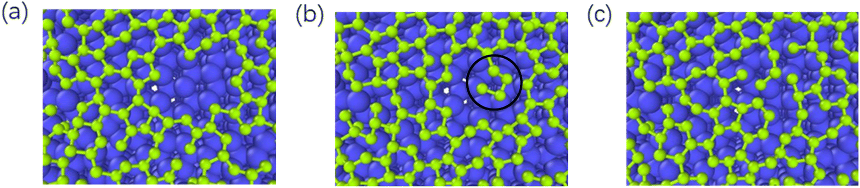
As reported by Zhu,39 the one-carbon molecule CHx (x = 1, 2, 3) fills in the lattice defects of graphene. In contrast, we use the deposition process of carbon atoms to observe the repair mechanism of graphene in detail. Fig. 9 represents the graphite deposition repair process at 2400 K. During the graphite deposition growth process, the unfilled portion of the substrate forms a larger defect (Fig. 9(a)), and the carbon atoms fill inside the defect during the subsequent growth process, polymerizing with the active carbon atoms on the large meta-ring to form a short chain (Fig. 9(b)), which rotates inward to ultimately form a smaller, closed carbon ring (Fig. 9(c)).
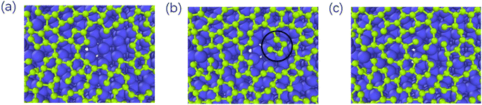 |
| | Fig. 9 (a)–(c) Represent the graphite deposition repair process at 2400 K (the circles mark the healing behavior of the graphene defects). | |
4.2 High temperature self-repair
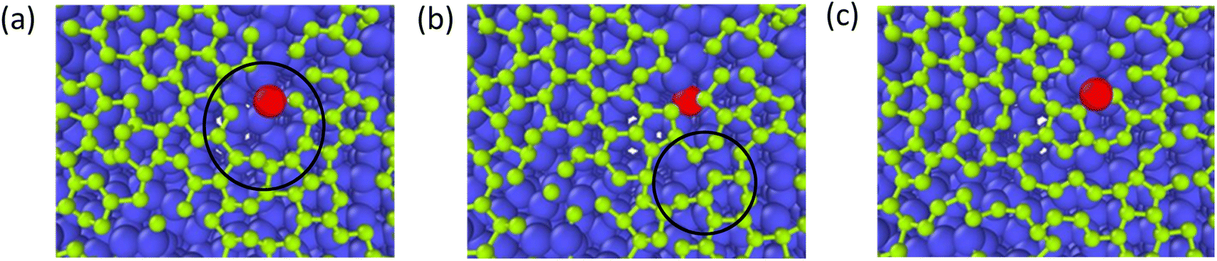
4.2.1 Diffusion processes of substrate atoms. In B.-y. Ju, W.-s. Yang report,41 graphene defect repair is caused by the combination of various minor vacancy defects to form a more significant defect and migrate to the edge for healing. In contrast, more vacancies need to be graphitized at higher temperatures (more than 2000 °C) to repair these holes through self-diffusion of carbon atoms, which is difficult to achieve in industry. Therefore, 2400 K was defined to make the deposited graphite for self-repair. Under the action of high temperature, the substrate atoms will diffuse into the deposited graphene layer. Fig. 10 represents the substrate diffusion repair process for the deposited graphene layer. The substrate carbon atoms by upward diffusion fill into the surface defects, and form a meta-ring with the deposited defective carbon atoms (Fig. 10(a)), at this time, the integrated graphite grid near the defects will be occasionally damaged due to the migration of atomic movement. The substrate diffusion atoms and the surface deposition carbon atoms are composed of the large meta-ring, which will crack into a number of small meta-ring (Fig. 10(b) and (c)).
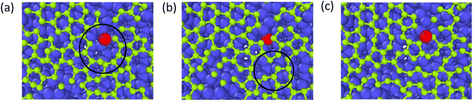 |
| | Fig. 10 (a)–(c) Represent the interdiffusion repair process between substrate and surface carbon atoms. (Red, blue are graphite substrate carbon atoms, green is deposited carbon atoms (the circles mark the healing behavior of the graphene defects)). | |
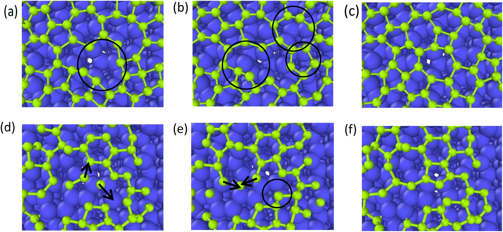
4.2.2 Atomic migration and dissociation self repair. The deposited carbon atoms will eventually form graphite-like lattices under sp2 hybridization bonding. Larger ring defects can also be directly decomposed into smaller defect grids due to heat treatment, and the defects are gradually repaired. Fig. 11 shows the cracking of large rings and atomic migration repair process of graphite mesh. In Fig. 11a–c, the graphite grid deposited on the substrate has significant defects. Under high temperature energy, the structure of the large ring is extremely unstable, and the carbon atoms on the large ring will directly split into two smaller rings, gradually splitting into a complete six element grid. In Fig. 11d and e, the carbon ring will attract nearby free carbon atoms and oligomers, forming branched chains, and then closing to form small rings. At the same time, the unstable large rings will gradually decompose and self-aggregate to form a complete graphite grid.
 |
| | Fig. 11 (a)–(c) Represent the dissociative repair of defects consisting of macrocycles; (d)–(f) represent the repair process in the vicinity of defects of carbon atom migration (the circle marks the healing behavior of graphene defects). | |
5 Growth process of multilayer a-GLM deposition
There have been numerous reports in the submicroscopic growth mechanism of pyrolytic graphite. Coffin and David31,32 proposed different growth mechanisms under different process conditions, respectively. Coffin believed that PyG grows layer-by-layer on substrates with different roughnesses, and grows in a layer-by-layer stacking, and the cone structure formed depends on the substrate surface roughness. The larger the substrate roughness profile size, the smaller the structural anisotropy of PyG deposited. David suggests that PyG is formed by the deposition of isolated island nuclei in the active sites of the substrate, which are “germ”-shaped nuclei formed by the rapid impact and merger of carbon atoms on the substrate surface. New graphite layers begin to be deposited concentrically around each island nucleus, forming pillars, which impact each other to form grain boundaries. Recently, it has been suggested that the growth mechanism is similar to the Volmer–Weber 3-D island growth model for epitaxial film growth.33 To further illustrate the microscopic process of pyrolytic graphite deposition, in this study, molecular dynamics was used to simulate the initial growth stacking model on an ideal natural graphite substrate within a total of 5000 ps.
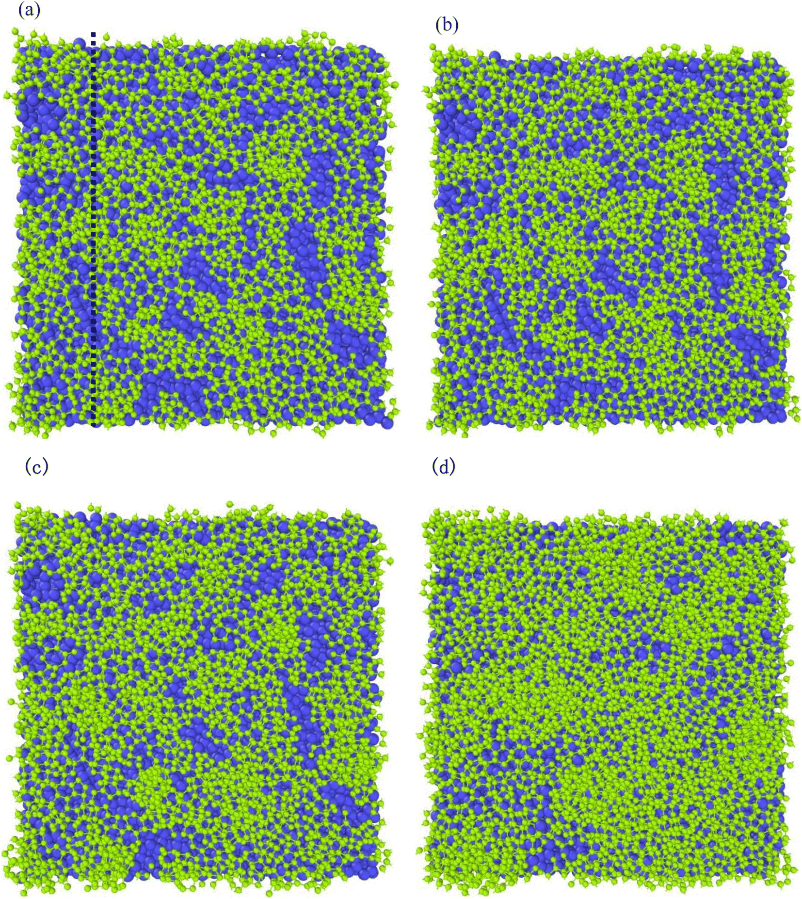
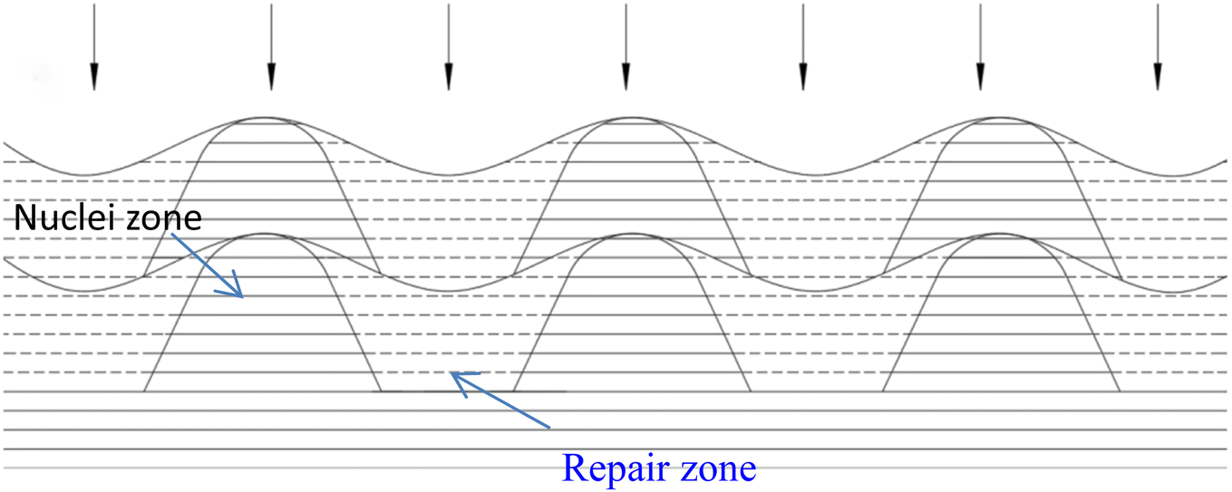
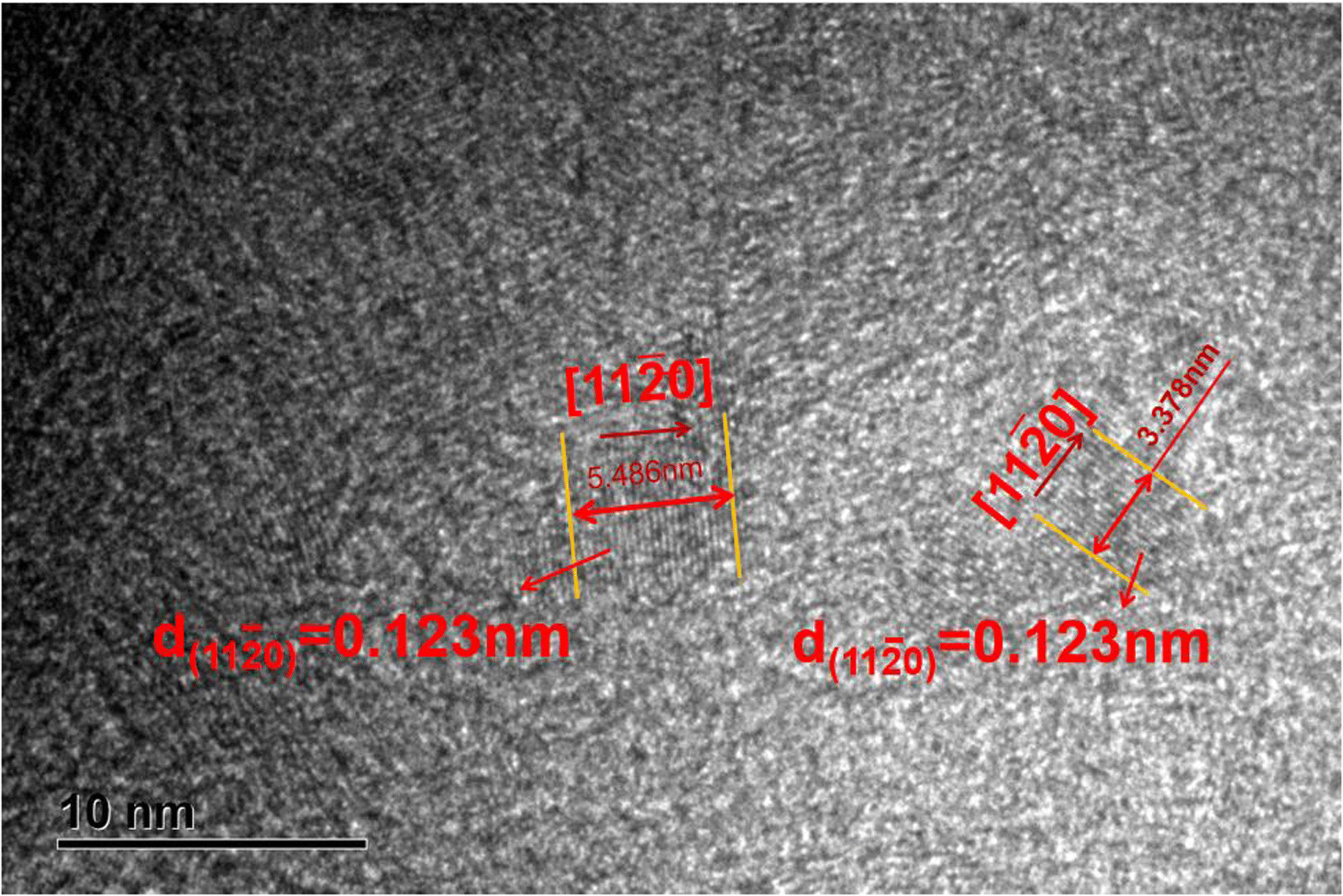
Fig. 12 and 13 represent side and top views of the a-GLM structures after deposition times of 2000–5000 ps at temperature of 2400 K. It is found that the deposition process of the a-GLM is not growing uniformly layer by layer, but the nuclei islands are preferred to grow (see Fig. 12). The specific growth process can be concluded that the first layer of local like-graphene at the high active points of substrate is formed (Fig. 12(a) and 13(a)) and the substrate leaves some blank zones, which indicates that a first like-graphene layer has many pore defects, and the covered domains prefer to grow to the uncover zones, and gradually form nuclei islands. From the side views of Fig. 12(a–d) and the top views of Fig. 13(a–d), it can be seen that the graphite-like structure prefers to grow at the high vibrating zone of the planar substrate, and the trend of carbon atom stacking in the whole wave planar surface is different due to the activity difference of different substrate zone, which leads to different energy of adsorbed carbon atoms presenting a concave–convex wave shape. This process can be presented by the schematic diagram of Fig. 14. The nuclei and repair zones belong to different active zones. The growth of carbon deposition on the active zones will be preferred and a nuclei island is formed. The zone around the nuclei islands belongs to the repair zone. For the real graphite produced from CVD, the mechanism of its growth can be inspired by the simulation. Fig. 15 shows an image of TEM of a commercial PG, from which it can be seen that the regular crystal microdomains are dispersed. The Bravais–Miller index of the crystallographic planes perpendicular to paper plane are labeled for the selected two larger regular crystal domains, which are identified for the equivalent crystallographic plane (01![[1 with combining macron]](https://www.rsc.org/images/entities/char_0031_0304.gif) 0). We can deduce the deposition process of pyrolytic graphite by CVD is analogue to our modelling result.
0). We can deduce the deposition process of pyrolytic graphite by CVD is analogue to our modelling result.
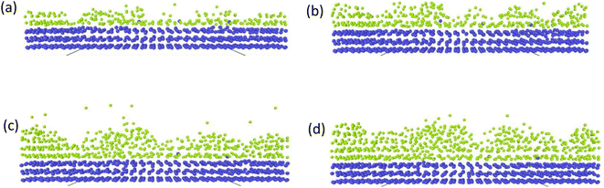 |
| | Fig. 12 Side views of the graphite-like structures stacked at deposition times of 2000–5000 ps at temperature 2400 K, after (a) 2000 ps; (b) 3000 ps; (c) 4000 ps; (d) 5000 ps. | |
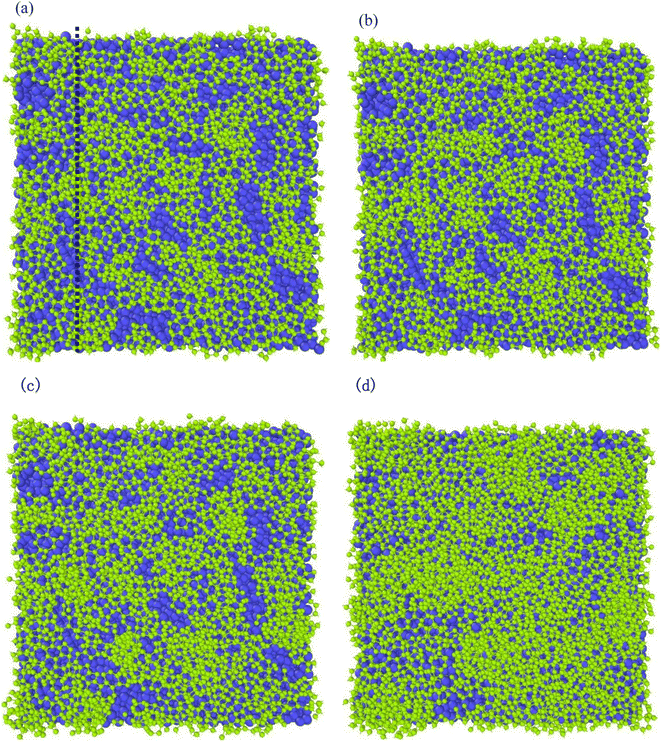 |
| | Fig. 13 Top views of graphite-like membrane structure deposited at temperature 2400 K after deposition time (a) 2000 ps, (b) 3000 ps, (c) 4000 ps, and (d) 5000 ps. | |
 |
| | Fig. 14 The schematic diagram of growth mechanism of multilayer pyrolytic graphite structure (the solid line indicates the carbon atoms deposited first and the dashed line indicates the carbon atoms deposited subsequently). | |
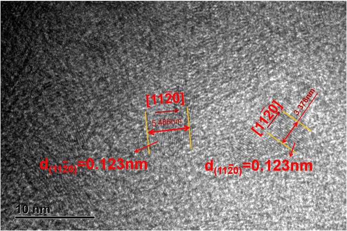 |
| | Fig. 15 The image of TEM of a commercial pyrolytic graphite (taken by JEM-2100F). | |
6 Conclusion
The microscopic growth process of the amorphous graphite-like film deposited on ideal graphite is studied by MD in the temperature range of 1500 K to 3000 K, and the optimal temperature is obtained about 2400 K from the integrity of the deposited film. In the monolayer like-graphite growth, low temperature is conducive to the nucleation of the substrate, appropriate high temperature to accelerate the carbon polymerization, the overall monolayer growth is mainly in the form of dendrites from the branched chain dissociation polymerization formation. In graphite defect repair, carbon atoms are subsequently deposited and attached inside the defects, repairing the defects caused by insufficient carbon atoms to form a six-membered cyclic lattice. In high-temperature relaxation repair, the substrate atoms diffuse upward to the surface to form new active spots in the defect traps, and the deposited carbon atoms also migrate to the vicinity of the defects on the substrate surface to assist the repair.
It can be deduced that the multilayer PyG structure is formed by first growth of monolayer graphene microdomains in the high-activity region, and being filled in the low-activity region. In this process, graphite defects near the high activity regions are also preferentially filled to be healed due to the higher ability to adsorb carbon atoms. The simulation results provide a more detailed understanding of the PyG growth mode at the microscopic level, which is helpful for industrial applications in the preparation of pyrolytic graphite by CVD.
Conflicts of interest
There are no conflicts to declare.
Acknowledgements
This work was financially supported by the National Key R&D Program of China (2019YFE03070001).
References
- T. Hirai and S. Yajima, J. Mater. Sci., 1967, 2, 18–27 CrossRef CAS.
- H. Pierson and M. Lieberman, Carbon, 1975, 13, 159–166 CrossRef CAS.
- P. Wang, M. Liu, T. Pei, L. Zhang, Z. Qie, X. Li, Y. Yu, M. Han, F. Sun and W. Zhou, AIP Adv., 2020, 10, 115007 CrossRef CAS.
- A.-S. Hadi and B. E. Hill, Sens. Actuators, A, 2020, 303, 111814 CrossRef CAS.
- M. A. Bento, S. Realista, A. S. Viana, A. M. Ferraria and P. N. Martinho, Sustainability, 2021, 13, 4158 CrossRef CAS.
- A. G. Turyanskiy and S. S. Gizha, X-Ray Spectrom., 2020, 49, 434–441 CrossRef CAS.
- A. Kren, T. Protasenia, A. Arnautov and V. Rudnitskii, Mech. Compos. Mater., 2015, 51, 225–230 CrossRef CAS.
- R. Hareesh, E. Vetrivendan, R. Sole and S. Ningshen, Appl. Surf. Sci., 2020, 529, 147106 CrossRef CAS.
- P. Zhu, M. Zhang, Q. Huang, K. Tong, J. Chen and G. Chen, Mater. Sci. Technol., 2015, 31, 1698–1705 CrossRef CAS.
- L. Zheng, Y. Wang, J. Qin, X. Wang, R. Lu, C. Qu and C. Wang, Vacuum, 2018, 152, 84–90 CrossRef CAS.
- J. Qin, C. Wang, Z. Yao, Z. Ma, X. Cui, Q. Gao, Y. Wang, Q. Wang and H. Wei, Ceram. Int., 2021, 47, 19213–19219 CrossRef CAS.
- X. Yang, G. Zhang, J. Prakash, Z. Chen, M. Gauthier and S. Sun, Int. Rev. Phys. Chem., 2019, 38, 149–199 Search PubMed.
- L. Wang, R. Lai, L. Zhang, M. Zeng and L. Fu, ACS Mater. Lett., 2022, 4, 528–540 Search PubMed.
- A. F. Fonseca, T. Liang, D. Zhang, K. Choudhary, S. R. Phillpot and S. B. Sinnott, ACS Appl. Mater. Interfaces, 2017, 9, 33288–33297 CrossRef CAS PubMed.
- C. Bauer, M. Ries and S. Pfaller, Soft Mater., 2022, 20, 428–443 CrossRef CAS.
- S. Yang, Sensors, 2021, 21, 2621 CrossRef CAS PubMed.
- R. Rasuli, K. Mostafavi and J. Davoodi, J. Appl. Phys., 2014, 115, 024311 CrossRef.
- L. Zhang, Y. Zhu, W. Teng, T. Xia, Y. Rong, N. Li and H. Ma, Comput. Mater. Sci., 2017, 130, 10–15 CrossRef CAS.
- K. Liu, E. Ren, J. Ma, Y. Cao, J. Du, W. Ming, X. Li and B. Li, J. Mater. Sci., 2020, 55, 4251–4264 CrossRef CAS.
- D. Huang, J. Pu, Z. Lu and Q. Xue, Surf. Interface Anal., 2012, 44, 837–843 CrossRef CAS.
- Z. Fu and Y. An, RSC Adv., 2016, 6, 91157–91162 RSC.
- B. Coyne, O. Zietz, S. Olson and J. Jiao, Microsc. Microanal., 2018, 24, 1624–1625 CrossRef.
- J. Park, J. Lee, J.-H. Choi, D. K. Hwang and Y.-W. Song, Sci. Rep., 2015, 5, 11839 CrossRef PubMed.
- O. J. Burton, F. C. Massabuau, V.-P. Veigang-Radulescu, B. Brennan, A. J. Pollard and S. Hofmann, ACS Nano, 2020, 14, 13593–13601 CrossRef CAS PubMed.
- G. Dhaliwal, P. B. Nair and C. V. Singh, Carbon, 2019, 142, 300–310 CrossRef CAS.
- Y. Umeno, Y. Yachi, M. Sato and H. Shima, Phys. E, 2019, 106, 319–325 CrossRef CAS.
- X. Yang, S. Wu, J. Xu, B. Cao and A. C. To, Phys. E, 2018, 96, 46–53 CrossRef CAS.
- Z. Hui and Y. Chang, Int. J. Mod. Phys. B, 2019, 33, 1950020 CrossRef CAS.
- J. Kang and H. Hwang, Mol. Simul., 2005, 31, 561–565 CrossRef CAS.
- D. W. Brenner, Phys. Rev. B: Condens. Matter Mater. Phys., 1990, 42, 9458–9471 CrossRef CAS PubMed.
- C. David, P. Sublet, A. Auriol and J. Rappeneau, Carbon, 1964, 2, 139–148 CrossRef CAS.
- I. Coffin Jr, J. Am. Ceram. Soc., 1964, 47, 473–478 CrossRef.
- W. J. Lee, J. Gunning, N. Burke and J. Patel, Carbon, 2012, 50, 4773–4780 CrossRef CAS.
- P. Süle and M. Szendrő, Surf. Interface Anal., 2014, 46, 42–47 CrossRef.
- S. A. Eftekhari, D. Toghraie, M. Hekmatifar and R. Sabetvand, Phys. E, 2021, 133, 114789 CrossRef CAS.
- A. R. G. Brown, A. R. Hall and W. Watt, Nature, 1953, 172, 1145–1146 CrossRef CAS.
- E. Vetrivendan, R. Hareesh and S. Ningshen, Thin Solid Films, 2022, 749, 139180 CrossRef CAS.
- D.-W. Choi, H. Park, J. H. Lim, T. H. Han and J.-S. Park, Carbon, 2017, 125, 464–471 CrossRef CAS.
- D. Zhu, H. Pu, P. Lv, Z. Zhu, C. Yang, R. Zheng, Z. Wang, C. Liu, E. Hu, J. Zheng, K. Yu, W. Wei, L. Chen and J. Chen, Carbon, 2017, 120, 274–280 CrossRef CAS.
- M. Cheng, R. Yang, L. Zhang, Z. Shi, W. Yang, D. Wang, G. Xie, D. Shi and G. Zhang, Carbon, 2012, 50, 2581–2587 CrossRef CAS.
- B.-y. Ju, W.-s. Yang, Q. Zhang, M. Hussain, Z.-y. Xiu, J. Qiao and G.-h. Wu, Int. J. Miner., Metall. Mater., 2020, 27, 1179–1190 CrossRef.
- Z. Chen, W. Ren, B. Liu, L. Gao, S. Pei, Z.-S. Wu, J. Zhao and H.-M. Cheng, Carbon, 2010, 48, 3543–3550 CrossRef CAS.
- J. K. Wassei, M. Mecklenburg, J. A. Torres, J. D. Fowler, B. Regan, R. B. Kaner and B. H. Weiller, Small, 2012, 8, 1289 CrossRef CAS.
- O. M. El-Ahwany, A. E. Awadallah, A. A. Aboul-Enein, S. M. Abdel-Azim, N. A. Aboul-Gheit and S. A. Abo-EL-Enein, Fullerenes, Nanotubes Carbon Nanostruct., 2020, 28, 435–445 CrossRef CAS.
- S. Rodríguez-Villanueva, F. Mendoza, B. R. Weiner and G. Morell, Nanomaterials, 2022, 12, 3033 CrossRef PubMed.
- N. Lümmen, Phys. Chem. Chem. Phys., 2010, 12, 7883–7893 RSC.
- X. Wang, Q. Yuan, J. Li and F. Ding, Nanoscale, 2017, 9, 11584–11589 RSC.
- M. Yang, S. Sasaki, K. Suzuki and H. Miura, Appl. Surf. Sci., 2016, 366, 219–226 CrossRef CAS.
- T. Kreuger, A. Bos and S. Kersten, Chem. Eng. J., 2022, 440, 135487 CrossRef CAS.
|
| This journal is © The Royal Society of Chemistry 2023 |
Click here to see how this site uses Cookies. View our privacy policy here. 
 Open Access Article
 This Open Access Article is licensed under a Creative Commons Attribution-Non Commercial 3.0 Unported Licence
 ab and
Zhang Xinjunc
ab and
Zhang Xinjunc