
 Open Access Article
 This Open Access Article is licensed under a Creative Commons Attribution-Non Commercial 3.0 Unported Licence
Dielectric constant enhancement of poly 4-vinylphenol (PVPh) via graphene flakes incorporation through electrospray atomization for energy storage†
Adnan Ali *,
Sosiawati Teke,
Ghayas Uddin Siddiqui and
Young Sun Mok
*,
Sosiawati Teke,
Ghayas Uddin Siddiqui and
Young Sun Mok
Department of Chemical Engineering, Jeju National University, Jeju 63243, Republic of Korea. E-mail: adali@jejunu.ac.kr; Fax: +82-64-755-3670; Tel: +82-64-754-3682
First published on 27th October 2023
Abstract
We report on the fabrication of hybrid composite poly 4-vinlyphenol (PVPh)/graphene thin film via cost-effective electrospray atomization deposition technique. Thin films fabricated through manipulating deposition technique in two different ways which are blending and layer by layer (LBL). For investigation of PVPh/graphene hybrid composite dielectric behavior in comparison to PVPh; three asymmetric MIS thin film capacitors were fabricated, where dielectric thin films (i) PVPh and (ii & iii) hybrid composite thin films PVPh/graphene (blended and LBL) were sandwiched between electrodes i.e. indium tin oxide (ITO) and p-type semiconductor poly(3,4-ethylenedioxythiophene) polystyrene sulfonate (PEDOT:PSS). The dielectric properties of the thin films were characterized for frequencies 1 to 100 kHz while utilizing the MIS thin film capacitors. The capacitance obtained at 1 kHz frequency for PVPh/graphene (LBL) dielectric layer at the voltage range ±10 volts was 8.5 mF cm−2 while for blended PVPh/graphene thin film the capacitance at the voltage range ±3 volts was 0.40 μF cm−2 and for pristine PVPh as dielectric layer the capacitance at voltage range ±1 volts was 1.45 μF cm−2. Similarly, even at higher frequencies up to 100 kHz, the PVPh/graphene (LBL) showed stable behavior. Thus, the composite PVPh/graphene (LBL) thin film has a better dielectric nature compared to the composite PVPh/graphene (blended) thin film, even at higher frequencies with larger operational voltage window. This distinguishing nature of the composite PVP/graphene (LBL) is attributed to increase in dielectric constant due to graphene flakes in between PVPh. For the thin films LBL and blended PVPh/graphene, the calculated dielectric constant at 10 kHz is 6.7 and 0.023 while at 100 kHz it is 2 and 0.0167, respectively.
1. Introduction
For energy storage purposes, batteries, fuel cells, and conventional (electrostatic) and electrochemical capacitors are often utilized.1–5 Among these, nanoscale capacitors are identified as the most auspicious for energy storage.6–8 Nanoscale capacitors have attained higher energy densities of numerous orders of magnitude. In nanoscale dielectric capacitors (NDCs), a dielectric material is sandwiched between the metallic layers to increase capacitance without changing capacitor dimensions, which can store and discharge the charge.9,10 They are more advantageous in a wide range of applications such as wearable devices, portable devices and implantable devices10–12 because they can charge/discharge at much quicker power rates, and have a longer lifespan with shorter load cycles than customary batteries.13Regarding materials, latest experimental and theoretical studies on metallic nanowires,14 carbon nanotubes and graphene15 have been emphasizing on determining the dielectric nature of such compositional structures, to employ in energy storage devices as thin films.16–20 Out of these materials, graphene flakes have been attracting researchers significant interest because of their distinctive features, such as high electrical and thermal conductivities, mechanical strength, and large surface area in various applications, including electronics, energy storage, and biocompatible implantation.21
Many researcher groups have been extensively employing 2D materials based composite thin films as dielectric layer in energy storage devices. Gupta et al.22 have selectively incorporated graphene oxide nanosheets and BaTiO3 NPs in a tri-layer device for studying the role of heterointerfaces within each layer and at the interfaces between each layer. The group has reported the formation of numerous microcapacitors due to numerous functional groups attached to the surface-induced interfacial polarization. A. Karim et al.23 research group has demonstrated the effect of confinement on the dielectric, electrical and capacitive energy storage properties of PVDF/GO and PVDF/rGO films within the measured frequency range. Due to embedment of rGO into PVDF, high dielectric constant values at low frequencies are produced by parallel microcapacitors. Similarly, Yambem et al.24 has reported the development of capacitive flexible pressure sensors usinging graphene based conductive foams. In conductive foams, graphene is used as coating on the pores in the foam, inside the foam structure or a combination of both. V. O. Özçelik et al.25 have reported on a nanoscale dielectric capacitor model. In their model, 2D materials have been studied and it is deduced that quantum effects become crucial at nanoscale and significantly affect the capacitor dimensions. Another research group, B. Man et al.26 have reported the graphene/insulator/graphene flexible and transparent tunable thin film capacitor. The fabricated capacitor has high dielectric tunability and bending durability.
From polymers, poly(4-vinylphenol) (PVPh) which belongs to the family of polyphenols, is a versatile polymer with various applications including organic field-effect transistors (OTFTs), organic photovoltaics (OPVs) and biomedical application.27–31 It has outstanding dielectric features which support efficient charge storage and control of charge carriers, high breakdown voltage, compatibility with solution processing techniques.32 In addition to this, it exhibits good thermal stability, which enables it to withstand high temperature processing without significant degradation.33 The research group of S. Singh has reported the employment of PVPh as dielectric in TFT fabricated via spin coating technique. The interface of dielectric/semiconductor has been studied in terms of capacitance and leakage current density. It has been reported that there is slow polarization that occurs in PVPh at threshold applied potential.34 Similarly, J. Park et al.35 has applied c-PVPh as dielectric thin film and has proposed the method for its surface-energy manipulation by exploiting the density-controllable soluble PVPh. It was investigated that by decreasing residual –OH groups on the surface, the electric dipoles due to –OH groups at semiconductor/insulator interface locally enhances the transport band and thus accelerates the charge transportation and enhancing the TFT performance.
The poly(4-vinylphenol) (PVPh)/graphene composite film combines the properties of both PVPh and graphene as a material with enhanced characteristics.36 When graphene flakes incorporated into a PVPh matrix, the synergic effect of both makes PVPh/graphene composite a potential candidate for applications such as conductivity enhancement, mechanical reinforcement, thermal stability, barrier properties (hydrophilic nature), against moisture and gas permeation and for energy storage devices, typically supercapacitors (SCs) and lithium ion batteries (LIBs).37 D. Roy33 has applied PVPh/GO nanocomposite as dielectric thin film and studied the dielectric and leakage current properties at frequencies ranging from 1 kHz to 1 MHz. It is observed that the dielectric constant increased due to the insulating nature of graphene. Yoo et al.38 group has reported the application of amorphous fluoropolymer CYTOP as a gate dielectric in MOS2 FET. In comparison, MoS2 FETs with the cross-linked PVP dielectric showed a better performance in terms of voltage threshold which is attributed to the surface dipole effect induced by the strong electron-withdrawing fluorine groups in CYTOP.
In this work, the PVPh, PVPh/graphene composite thin films (LBL and blended) were fabricated using electrospray. Electrospray deposition parameters of respective solution/dispersion of PVPh and graphene flakes were optimized for thin films fabrication on ITO coated glass substrate.39–42 Using the optimized parameters of electrospray deposition, composite thin films of PVPh and graphene have fabricated by layer by layer (LBL) and blending deposition on ITO coated glass substrate. For dielectric nature and capacitive behavior investigation the thin films PVPh and PVPh/graphene (LBL and blended) were sandwiched between ITO and (PEDOT:PSS) electrodes. MIS characterizations have shown that composite thin film PVPh/graphene (LBL) charge storage capacity, and operating voltage window is far better in comparison to thin films PVPh/graphene (blended) and pristine PVPh, are far better. Therefore, PVPh/graphene (LBL) is more viable fabrication method of the composite PVPh/graphene thin film for application in electronic devices as dielectric layer. The charge storage capacity enhancement of the composite this film is attributed to increase in dielectric constant and microcapacitors formations at the interfaces of PVPh and graphene due to functional groups on the surfaces of both materials.
2. Materials and analysis
Poly 4-vinlyphenol (PVPh) and N-methyl-pyrrolidone (NMP) solvent purchased from Sigma Aldrich while and graphene nanoplatelets (<4 layers and surface area > 750 m2 g−1) purchased from Cheap Tubes, were used in this research. The PVPh powder 75 mg ml−1 was dissolved in NMP solvent; then cross-linking agent (CLA) was added to it. After dissolution, for better solubility of PVPh powder, the solution was ultra-sonicated for 10 minutes with 60% amplitude. The viscosity of the ink was measured to be 13.2 mPa by using ViscometerVM-10A system. The surface tension of the ink was measured to be 10.05 mN m−1. The conductivity of the PVPh ink was 0.35 μS cm−1, measured by conductivity meter (Cond6+ meter). Similarly, the graphene flakes 1 mg ml−1 was dispersed in NMP solvent using ultrasonication for 30 minutes at 3 s on 1 s off and kept the amplitude at 60%. The viscosity of the dispersion measured as 15 mPa and surface tension measured as 57–59 mN m−1. The electrical conductivity measured as 12.0 μS cm−1. For PVPh/graphene ink synthesis, ultrasonication was carried out for 40 minutes at RT to well disperse the 0.90 mg graphene nano flakes and 0.30 g poly 4-vinlyphenol (PVPh) in 4 ml of NMP solvent. The viscosity of the solution containing PVPh/graphene measured was 22.3 mPa and surface tension was measured 20–24 mN m−1. The electrical conductivity of the supernatant containing PVPh/graphene was measured as 20 μS cm−1.3. Experimental setup and electrospray phenomena analysis for thin film fabrication
The electrospray setup details are as follows which is used for thin films fabrication, schematic is given in Fig. S1.† The respective dispersion was injected into an ink chamber (Nano NC Nozzle adaptor) via syringe pump (Hamilton, Model 1001 GASTIGHT syringe) and to the nozzle a steady flow rate was provided, which was connected to the chamber via the syringe pump. For the building up of the anticipated electric field, a metal nozzle with an interior diameter of 710 μm [Havard 33G] was use as anode and was connected to a Trek Model 610E high voltage supplier. The ground was given by linking the voltage source's ground terminal to a stage which is capable of rotating at certain speed as well as serving as substrate holder. For taking images of the atomization events occurring at the nozzle tip, a high-speed camera was connected to the portable computer while putting a high intensity source of light opposite to it across the electrospray set-up.The stand-off distance was set at 15 mm, and the electrospray tests were first conducted with flow rates ranging from 50 to 1000 μl h−1 to identify the ideal spraying conditions. The potential difference between the anode nozzle and the grounded stage was gradually raised for each flow rate to improve the intensity of the electric field.43–45 Applying a different voltage at each flow rate step results in different forms of atomization, and as a result, diverse modes were seen, from dripping to the multi-jet.46–49 The obtained operational envelopes of the PVPh, graphene flakes and PVPh/graphene dispersions subjected to varying high voltages at different flow rates to observe electrospray atomization modes have been summarized in Fig. 1a–c. The respective envelope for each dispersion makes it clear that the needed applied voltage rose from one mode to another as the flow rate increased which is due to the amount of respective dispersion accumulation at the nozzle orifice. The other associated reason for this rise in applied voltage is to overcome the surface tension and generate a stable cone-jet for uniform deposition.
 | ||
| Fig. 1 Electrospray Atomization operating envelops for (a) PVPh, (b) graphene flakes and (c) PVPh/graphene flakes. | ||
3.1. Pristine PVPh and composite PVPh/graphene thin films fabrication
The ITO coated glass substrate was rinsed with deionized water and then dried before the thin film deposition.After that, the respective dispersion was electrostatically atomized in the stable cone jet modes by utilizing optimized parameters obtained through developed operating envelop which are, applied flow rate of 300 μl h−1 and a potential of 2.3 kV, 3.8 kV and 5.3 kV for PVPh, graphene flakes, PVPh/graphene blended, respectively. To observe the deposition area, the stand-off was gradually increased from 5 mm to 20 mm. To determine the ideal value, the moving substrate's speed was varied from 1 mm s−1 to 3 mm s−1. It was noticed that for covering (2 × 2) cm2 area on ITO coated glass substrate, optimum parameters of stand-off and velocity were 15 mm and 3 mm s−1, respectively. Schematic of the deposition of thin films from solution via utilizing electrospray set-up is given in Fig. 2. The deposited thin films on ITO substrate were cured at 200 °C treated for two hours.
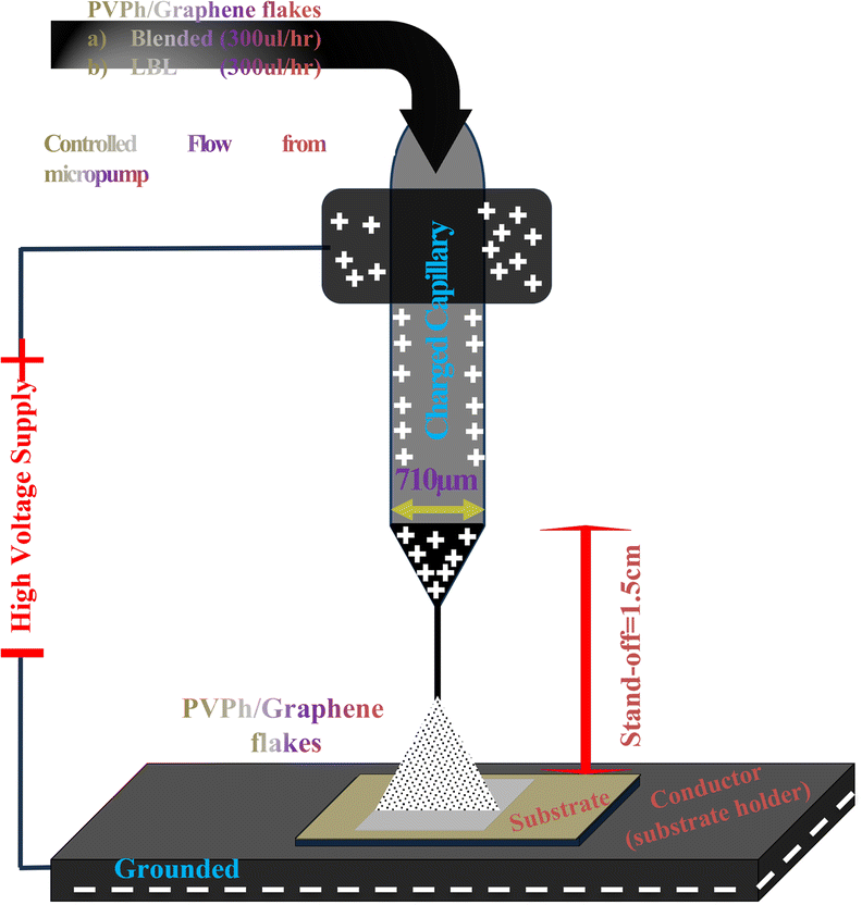 | ||
| Fig. 2 Schematic of electrospray system operation and mechanism. | ||
In Fig. 3A and B, higher resolution and high-speed shots of the atomization events from meniscus to multi-jets (a–f) taking place at flow rate 300 μl h−1 with varying applied voltages for PVPh, graphene flakes and PVPh/graphene dispersions have shown respectively. In Fig. 3B, variation in applied voltage requirement for various atomization events (dripping to multi-jets) w.r.t. flow increase of each dispersion has been compared. It has been observed that stable jet with flow rate increase has obtained at lower applied voltage for PVPh as compared to graphene and PVPh/graphene dispersions. In case of PVPh/graphene dispersion, the stable jet with flow rate increase, ranging from 100 to 1000 μl h−1 has obtained at more than 5 kV. This increase in applied voltage requirement could be attributed to higher surface tension values plus viscosity of the respective dispersion.
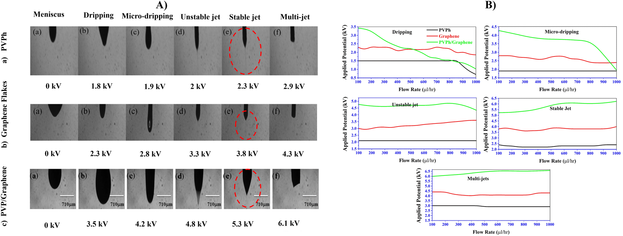 | ||
| Fig. 3 Electrospray atomization events (A) individual and (B) comparison of dripping to multi-jets for PVPh, graphene and PVPh/graphene at applied voltages and varying flow rate. | ||
3.2. Results, characterizations and discussion
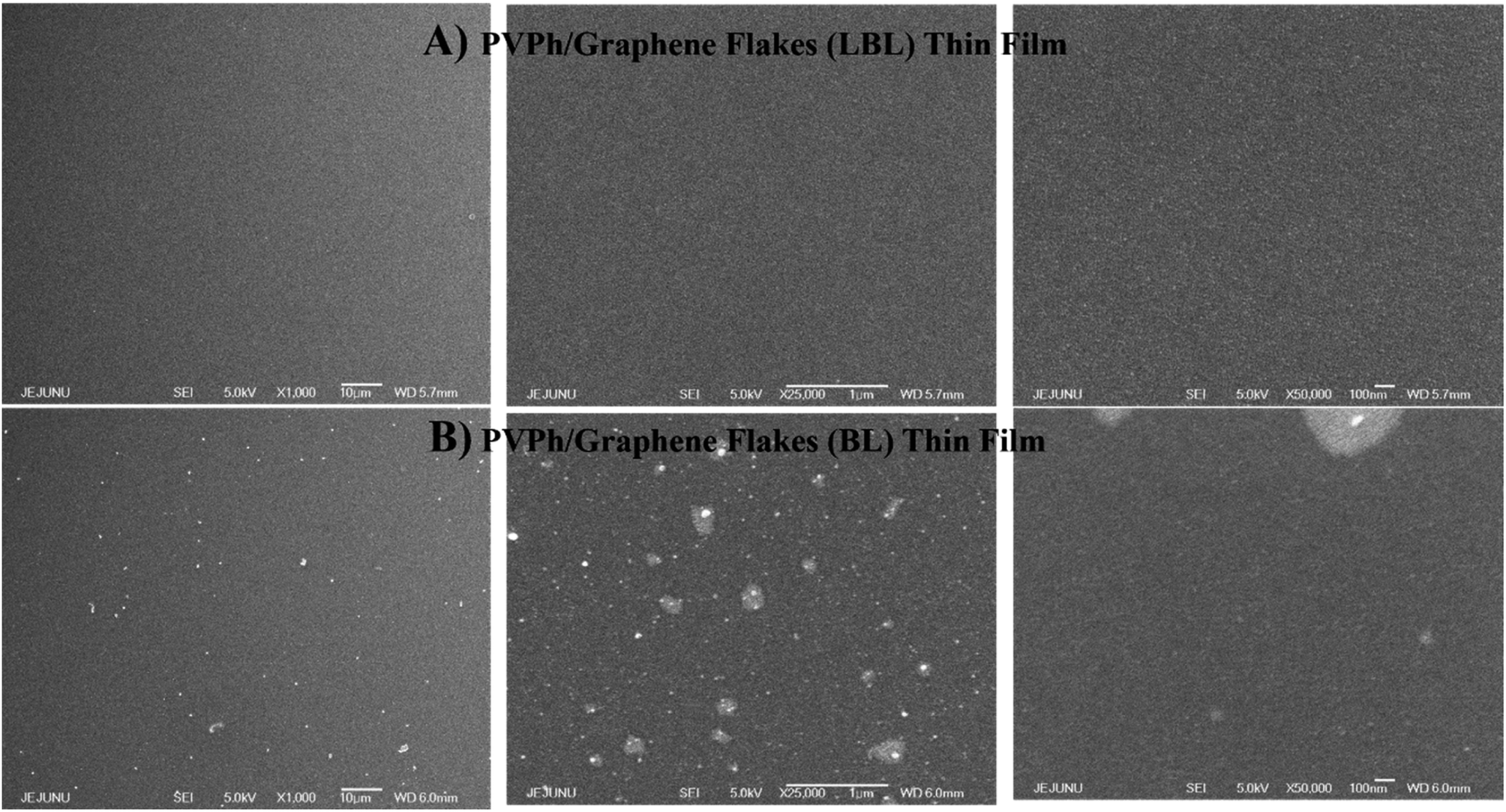 | ||
| Fig. 4 Lower to higher resolution FESEM surface morphology analysis of PVPh/graphene thin films: (A) LBL and (B) blended. | ||
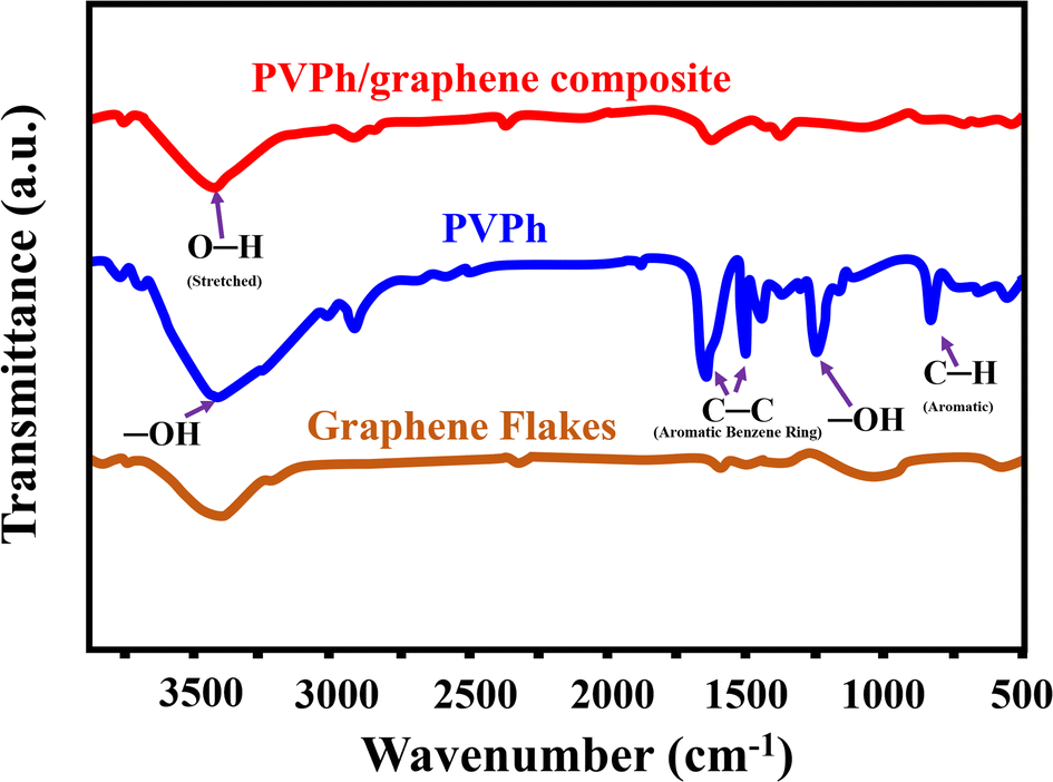 | ||
| Fig. 5 Comparison of FT-IR spectroscopy of graphene flakes, PVPh and PVPh/graphene. | ||
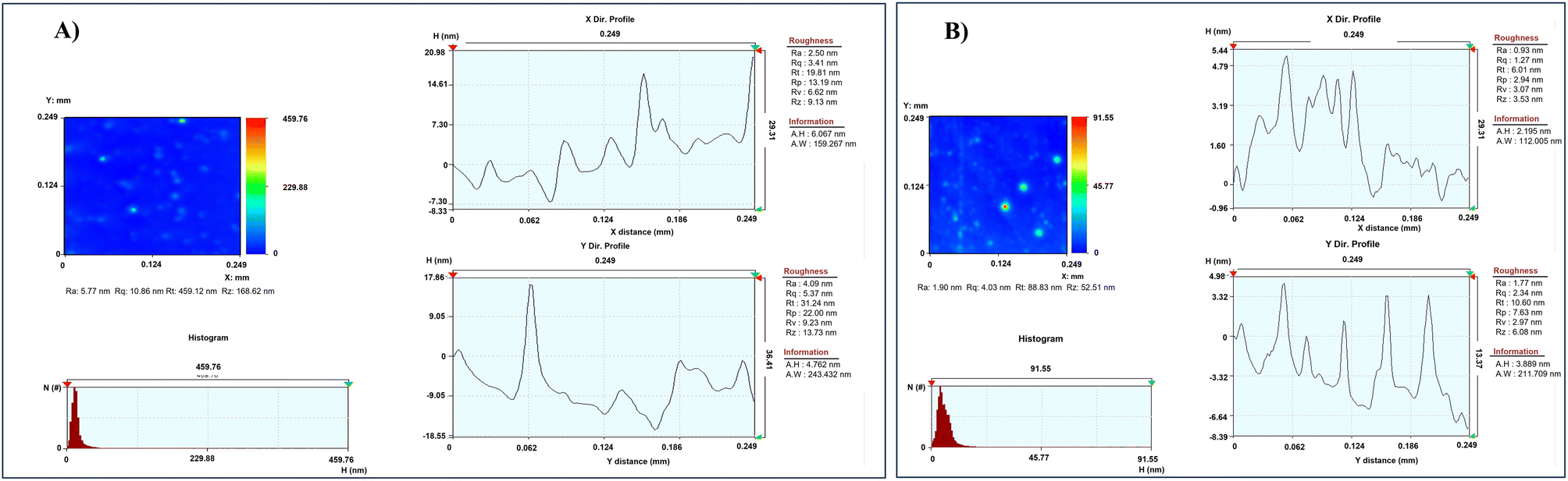 | ||
| Fig. 6 X and Y direction surface profilometry analysis of the composite PVPh/graphene (A) blended and (B) LBL thin films. | ||
4. Electrical behavior investigation
4.1. Metal–insulator–semiconductor (MIS) devices fabrication
Metal–Insulator–Semiconductor (MIS) capacitor device structures were fabricated on cleaned ITO-coated (1 μm) glass substrates to examine and compare the dielectric nature of the composite PVPh/graphene (LBL and blended) and PVPh thin films. PEDOT:PSS (180 nm) thin film (2 × 2) cm2 was deposited on top of the dielectric layer PVPh, PVPh/graphene through electrospray atomization, schematic of MIS configuration is shown in Fig. 7.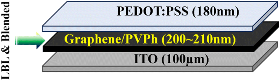 | ||
| Fig. 7 Schematic of MIS capacitor having PVPh/braphene (LBL & blended) as dielectric layer. | ||
4.2. Electrical properties of pristine PVPh and composite PVPh/graphene thin films
MIS capacitors fabricated with configuration where PEDOT:PSS applied as top electrode and ITO as bottom electrode while PVPh, PVPh/graphene (LBL & blended) sandwiched in between for investigating the dielectric properties of the respective thin films. The thicknesses of composite PVPh/graphene thin films were ∼210 nm (LBL) and ∼200 nm (blended). The best enhanced electrical behavior has been observed for the composite PVPh/graphene (LBL) thin film as compared to PVPh and PVPh/graphene (blended). To investigate the charge storage mechanism, a capacitance–voltage (CV) measurement was carried out for the device with various AC frequencies. With an input frequency of 1 kHz, shown in Fig. 8, illustrating the CV analysis of MIS capacitors having PVPh and composite PVPh/graphene (LBL & blended) thin films, respectively. With a maximum capacitance of 8.42 mF cm−2 in the voltage range of 0.1 to 1.80 V, PVPh/graphene (LBL) film has been found to exhibit better dielectric nature. In the inset of Fig. 8, at an enlarged scale, capacitance of PVPh and PVPh/graphene (blended) thin film has been highlighted and this comparison of capacitance values makes it more obvious that the composite PVPh/graphene (LBL) thin film has 103 times more capability of charge storage at a larger operation window i.e. ± 10 volts and with more stability.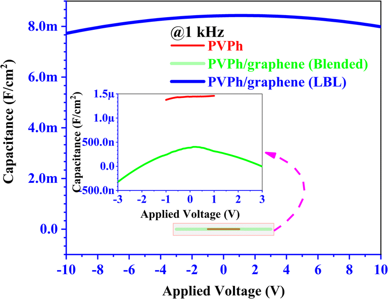 | ||
| Fig. 8 Capacitance comparison of PVPh and PVPh/graphene (LBL & blended) thin films in MIS configuration. Inset graph showing the enlarged scale capacitance of PVPh and PVPh/graphene (blended). | ||
Capacitance dispersion, series resistance, and bulk resistance are all factors that may have an impact on the capacitor's behavior.53 The performance of MIS capacitors at higher frequencies is shown in Fig. 9A and B, where PVPh/graphene (LBL & blended) applied as dielectric layers. While PVPh thin film based MIS capacitor CV, Cf and έf characterization output have been shown in Fig. S6A–C.† As with an increase in AC frequency, the capacitor's capacitance decreases. It has been observed that the composite PVPh/graphene (LBL) dielectric thin film performs 104 orders better than the PVPh/graphene (blended) thin film at higher frequencies up to 100 kHz and high voltage. When used as a dielectric layer, this behavior is far superior to pristine PVPh or PVPh/graphene (blended) composite thin films. These characteristics demonstrate an excellent charge storage mechanism and have shown small variations even at higher frequencies for the composite PVPh/graphene LBL thin film based MIS capacitor. Fig. 9 shows plots measured for frequency dependent capacitance density (C vs. f) in the MIS configuration at various frequencies ranging from 10 kHz to 100 kHz. When the frequency was increased from 10 kHz to 100 kHz, the capacitance density of the ∼200 nm thick hybrid dielectric PVPh/graphene (blended) thin film dropped from 4.07 to 2.96 μF cm−2. Similarly, for ∼210 nm thick hybrid dielectric PVPh/graphene (LBL) film for frequency increase, from 10 kHz to 100 kHz, the capacitance density decreased from 1.18 to 0.358 mF cm−2. The drop in capacitance density is ∼27.27% for PVPh/graphene (blended) and ∼74% for PVPh/graphene (LBL). But it is worthy to note that the capacitance density of PVPh/graphene (LBL) is ∼99.70% more at 10 kHz, compared to PVPh/graphene (blended) and similarly, at higher frequency of 100 kHz the capacitance density is ∼99.1% more. Therefore, the overall PVPh/graphene (LBL) dielectric thin film capacitance density capability is ∼100% more than PVPh/graphene (blended). As the dielectric constant is a function of frequency, as the frequency increased from 10 kHz to 100 kHz, the value of dielectric constant decreased due to polarization mechanisms.
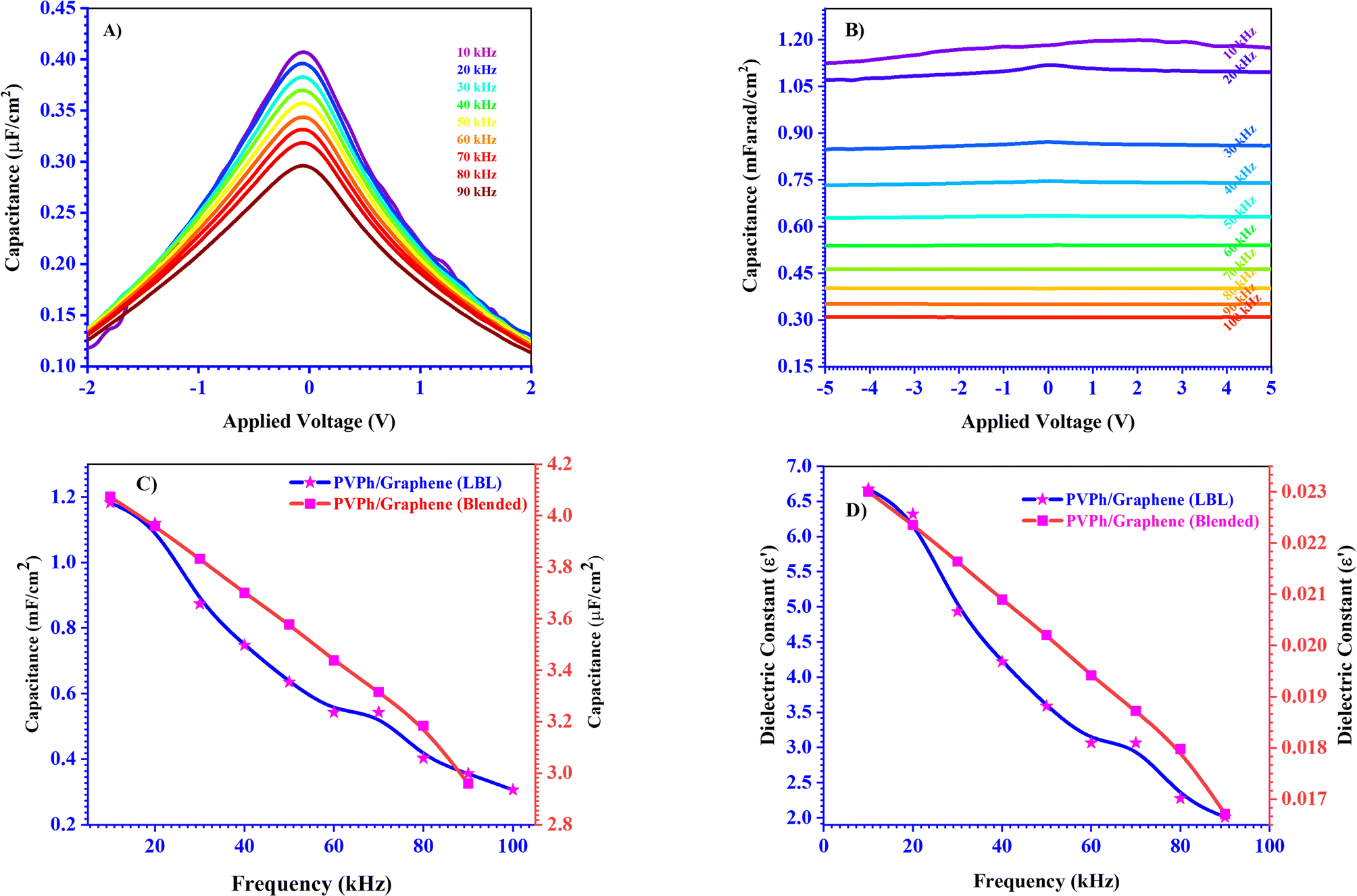 | ||
| Fig. 9 (A & B) Capacitance vs. applied voltage (CV) at different frequencies, (C) frequency dependent capacitance (Cf) and (D) frequency dependent dielectric constant (έf), characterization of the composite PVPh/graphene (blended and LBL) thin film applied as dielectric layer in the MIS capacitor. | ||
4.3. Mechanism of capacitance enhancement of PVPh by graphene flakes doping
It has been observed that PVPh/graphene (LBL) CV performance at lower to higher frequencies is far better in comparison to blended and pristine PVPh. This behavior could be attributed to the interaction between –OH in PVPh and functional groups present at graphene flakes surface. In LBL composite thin film the more –OH of PVPh and functional groups at the surface of the graphene flakes interact easily and leading to the formation of local microsupercapacitors which contribute to the overall accumulated capacitance of the LBL composite. These microsupercapacitor are noticed to be stable even at higher frequencies and contributing a reasonable accumulated capacitance to the overall obtained capacitance. While in blended PVPh/graphene composite thin film, the –OH in PVPh and functional groups at graphene surface are not systematically available for making more localized microsupercapacitors formation which led to the overall almost 10k times lesser capacitance compared to LBL composite thin film. Therefore, from lower to higher frequencies the –OH from PVPh and surface functional groups in grpahene flakes are seized and the probability of microsupercapacitor formation is not possible or almost negligible. In short, LBL provides more sites for microsupercapacitor formation as compared to blended thin film.5. Conclusion
PVPh/graphene composite thin films are fabricated using electrospray technique through blending and LBL. It has been observed through investigation that composite PVPh/graphene (LBL) thin film has shown better capacitance compared to the PVPh/graphene (blended). Besides this, the behavior of composite PVPh/graphene (LBL) thin film is much more stable at lower (1 kHz) as well as higher frequencies (100 kHz) compared to PVPh/graphene (blended) thin film. It has been observed that voltage operating window of PVPh/graphene (LBL) is broader than pristine PVPh and PVPh/graphene (blended). This characteristic of PVPh/graphene thin film can be attributed to the increase in dielectric constant increase and microcapacitors formation at the interfaces which are more favourable in case of PVPh/graphene (LBL) compared to blended thin film.Author contributions
A. A.: conceptualization, methodology, investigation, visualization, writing original draft; S.T.: data curation, formal analysis, writing review and editing; G. U. S.: validation, writing – review and editing; Y. S. M: supervision, funding acquisition and validation.Conflicts of interest
The authors declare that they have no known competing financial interests or personal relationships that could have appeared to influence the work reported in this paper.Acknowledgements
This research was supported by Brain Pool program (2022H1D3A2A02060361) and Basic Science Research Program (2021R1A4A2000934) funded by the Ministry of Science and ICT through the National Research Foundation of Korea.References
- B. K. Saikia, S. M. Benoy, M. Bora, J. Tamuly, M. Pandey and D. Bhattacharya, Fuel, 2020, 282, 118796 CrossRef CAS.
- A. G. Pandolfo and A. F. Hollenkamp, J. Power Sources, 2006, 157, 11–27 CrossRef CAS.
- A. Bhardwaj, J. N. Pagaduan, Y.-G. Yu, V. J. Einck, S. Nuguri, R. Katsumata and J. J. Watkins, ACS Appl. Mater. Interfaces, 2021, 13, 61027–61038 CrossRef CAS PubMed.
- H.-C. Chen, L.-Y. Hou, C. He, P.-J. Laing, C.-Y. Huang and W.-S. Kuo, ACS Appl. Energy Mater., 2022, 5, 8262–8272 CrossRef CAS.
- M. Winter and R. J. Brodd, Chem. Rev., 2004, 104, 4245–4270 CrossRef CAS PubMed.
- J. M. Lim, Y. S. Jang, H. Van T. Nguyen, J. S. Kim, Y. Yoon, B. J. Park, D. H. Seo, K.-K. Lee, Z. Han, K. Ostrikov and S. G. Doo, Nanoscale Adv., 2023, 5, 615–626 RSC.
- J. Castro-Gutiérrez, A. Celzard and V. Fierro, Front. Mater., 2020, 7, 217 CrossRef.
- G. Gautham Prasad, N. Shetty, S. Thakur, Rakshitha and K. B. Bommegowda, IOP Conf. Ser.: Mater. Sci. Eng., 2019, 561, 012105 CrossRef.
- D. Krueger, Z. Legenzoff, A. Wolf, J. Claypool, R. Schwartz and W. Huebner, J. Ceram. Sci. Technol., 2022, 13, 1–8 Search PubMed.
- M. Stengel and N. A. Spaldin, Nature, 2006, 443, 679–682 CrossRef CAS PubMed.
- J.-K. Huang, Y. Wan, J. Shi, J. Zhang, Z. Wang, W. Wang, N. Yang, Y. Liu, C.-H. Lin, X. Guan, L. Hu, Z.-L. Yang, B.-C. Huang, Y.-P. Chiu, J. Yang, V. Tung, D. Wang, K. Kalantar-Zadeh, T. Wu, X. Zu, L. Qiao, L.-J. Li and S. Li, Nature, 2022, 605, 262–267 CrossRef CAS PubMed.
- A. G. Olabi, M. A. Abdelkareem, T. Wilberforce and E. T. Sayed, Renewable Sustainable Energy Rev., 2021, 135, 110026 CrossRef CAS.
- A. Burke, Appl. Sci., 2021, 11, 8063 CrossRef CAS.
- Y. Zhou, S. Chen, D. Wu, L. Liu, H. Luo and D. Zhang, Compos. Commun., 2019, 16, 11–19 CrossRef.
- Z. Chen, L. Xie, X. Huang, S. Li and P. Jiang, Carbon, 2015, 95, 895–903 CrossRef CAS.
- S. Huang, Y. Liu, Y. Zhao, Z. Ren and C. F. Guo, Adv. Funct. Mater., 2019, 29, 1805924 CrossRef.
- C. Zhang and V. Nicolosi, Energy Storage Mater., 2019, 16, 102–125 CrossRef.
- S. Sorel, U. Khan and J. N. Coleman, Appl. Phys. Lett., 2012, 101(10), 103106 CrossRef.
- J.-Y. Lee, S. T. Connor, Y. Cui and P. Peumans, Nano Lett., 2008, 8, 689–692 CrossRef CAS PubMed.
- X. Han, S. Chen, X. Lv, H. Luo, D. Zhang and C. R. Bowen, Phys. Chem. Chem. Phys., 2018, 20, 2826–2837 RSC.
- B. I. Morshed, M. R. Momota and T. Fujiwara, IEEE International Conference on Electro Information Technology, 2023, pp. 509–513 Search PubMed.
- R. B. Prateek, A. Sarkar, S. Anand, A. Garg and R. Gupta, Energy Technol., 2021, 9 DOI:10.1002/ente.202000905.
- F. H. Likhi, M. Singh, S. V. Chavan, T. Cao, M. Shanbedi and A. Karim, ACS Appl. Nano Mater., 2023, 6, 11699–11714 CrossRef CAS.
- L. A. Kurup, C. M. Cole, J. N. Arthur and S. D. Yambem, ACS Appl. Nano Mater., 2022, 5, 2973–2983 CrossRef CAS.
- V. O. Özçelik and S. Ciraci, J. Phys. Chem. C, 2013, 117, 15327–15334 CrossRef.
- B. Man, S. Xu, S. Jiang, A. Liu, S. Gao, C. Zhang, H. Qiu and Z. Li, Nanoscale Res. Lett., 2015, 10, 279 CrossRef PubMed.
- Y. Li, Inkjet printing of thin film transistors, PhD thesis, University of Nottingham, 2021.
- K. H. Choi, A. Ali, H. C. Kim and M. T. Hyun, J. Korean Phys. Soc., 2013, 62, 269–274 CrossRef CAS.
- A. Ali, K. Ali, H. W. Dang, K. A. Mahmoud and K. H. Choi, J. Mater. Sci.: Mater. Electron., 2015, 26, 2039–2044 CrossRef CAS.
- T. H. Kim, C. G. Han and C. K. Song, Thin Solid Films, 2008, 516, 1232–1236 CrossRef CAS.
- S. Bhadauriya, PhD thesis, The University of Akron, 2019.
- S. Chaudhary, M. P. Joshi and V. Singh, Microelectron. Eng., 2018, 198, 85–92 CrossRef.
- D. Roy, Dielectric property study of poly(4-vinylphenol)–graphene oxide nanocomposite thin film, 2018 Search PubMed.
- S. Singh, Flexible Printed Electron., 2023, 8, 015011 CrossRef.
- J.-H. Kwon, J. Lee, M.-H. Kim, J.-H. Bae and J. Park, Org. Electron., 2021, 99, 106345 CrossRef CAS.
- J. Choi and H. Yoo, Polymers, 2023, 15, 1395 CrossRef CAS PubMed.
- Y. Li, R. Torah, S. Beeby and J. Tudor, 2012.
- G. Yoo, S. L. Choi, S. Lee, B. Yoo, S. Kim and M. S. Oh, Appl. Phys. Lett., 2016, 108, 263106 CrossRef.
- A. Tewari and S. Böhm, in Smart Multifunctional Nano-inks, ed. R. K. Gupta and T. A. Nguyen, Elsevier, 2023, pp. 197–226, DOI:10.1016/B978-0-323-91145-0.00006-2.
- D. Li, M. B. Müller, S. Gilje, R. B. Kaner and G. G. Wallace, Nat. Nanotechnol., 2008, 3, 101–105 CrossRef CAS PubMed.
- N. A. Kotov, I. Dékány and J. H. Fendler, Adv. Mater., 1996, 8, 637–641 CrossRef CAS.
- A. Jiříčková, O. Jankovský, Z. Sofer and D. Sedmidubský, Materials, 2022, 15(3), 920 CrossRef PubMed.
- M. S. Onses, E. Sutanto, P. M. Ferreira, A. G. Alleyne and J. A. Rogers, Small, 2015, 11, 4237–4266 CrossRef CAS PubMed.
- A. Jaworek, A. T. Sobczyk and A. Krupa, J. Aerosol Sci., 2018, 125, 57–92 CrossRef CAS.
- K. H. Choi, A. Ali, A. Rahman, N. Malik Mohammad, K. Rahman, A. Khan, S. Khan and D. S. Kim, J. Micromech. Microeng., 2010, 20, 075033 CrossRef.
- J. Xie, J. Jiang, P. Davoodi, M. P. Srinivasan and C.-H. Wang, Chem. Eng. Sci., 2015, 125, 32–57 CrossRef CAS PubMed.
- J. Rosell-Llompart, J. Grifoll and I. G. Loscertales, J. Aerosol Sci., 2018, 125, 2–31 CrossRef CAS.
- C. Cong, X. Li, W. Xiao, J. Li, M. Jin, S. H. Kim and P. Zhang, Nanotechnol. Rev., 2022, 11, 3305–3334 CrossRef CAS.
- R. P. A. Hartman, D. J. Brunner, D. M. A. Camelot, J. C. M. Marijnissen and B. Scarlett, J. Aerosol Sci., 1999, 30, 823–849 CrossRef CAS.
- S. Bose, T. Kuila, A. K. Mishra, R. Rajasekar, N. H. Kim and J. H. Lee, J. Mater. Chem., 2012, 22, 767–784 RSC.
- H. Bourara, S. Hadjout, Z. Benabdelghani and A. Etxeberria, Polymers, 2014, 6, 2752–2763 CrossRef.
- S.-C. Shiu and J.-L. Tsai, Composites, Part B, 2014, 56, 691–697 CrossRef CAS.
- J. Sun, B. Luo and H. Li, Adv. Energy Sustainability Res., 2022, 3, 2100191 CrossRef.
Footnote |
| † Electronic supplementary information (ESI) available. See DOI: https://doi.org/10.1039/d3ra06224d |
| This journal is © The Royal Society of Chemistry 2023 |