DOI:
10.1039/D3RA06137J
(Paper)
RSC Adv., 2023,
13, 31330-31345
Boosting efficiency above 28% using effective charge transport layer with Sr3SbI3 based novel inorganic perovskite†
Received
8th September 2023
, Accepted 19th October 2023
First published on 30th October 2023
Abstract
Strontium antimony iodide (Sr3SbI3) is one of the emerging absorbers materials owing to its intriguing structural, electronic, and optical properties for efficient and cost-effective solar cell applications. A comprehensive investigation on the structural, optical, and electronic characterization of Sr3SbI3 and its subsequent applications in heterostructure solar cells have been studied theoretically. Initially, the optoelectronic parameters of the novel Sr3SbI3 absorber, and the possible electron transport layer (ETL) of tin sulfide (SnS2), zinc sulfide (ZnS), and indium sulfide (In2S3) including various interface layers were obtained by DFT study. Afterward, the photovoltaic (PV) performance of Sr3SbI3 absorber-based cell structures with SnS2, ZnS, and In2S3 as ETLs were systematically investigated at varying layer thickness, defect density bulk, doping density, interface density of active materials including working temperature, and thereby, optimized PV parameters were achieved using SCAPS-1D simulator. Additionally, the quantum efficiency (QE), current density–voltage (J–V), and generation and recombination rates of photocarriers were determined. The maximum power conversion efficiency (PCE) of 28.05% with JSC of 34.67 mA cm−2, FF of 87.31%, VOC of 0.93 V for SnS2 ETL was obtained with Al/FTO/SnS2/Sr3SbI3/Ni structure, while the PCE of 24.33%, and 18.40% in ZnS and In2S3 ETLs heterostructures, respectively. The findings of this study contribute to in-depth understanding of the physical, electronic, and optical properties of Sr3SbI3 absorber perovskite and SnS2, ZnS, and In2S3 ETLs. Additionally, it provides valuable insights into the potential of Sr3SbI3 in heterostructure perovskite solar cells (PSCs), paving the pathway for further experimental design of an efficient and stable PSC devices.
1. Introduction
The development of perovskite materials as potential substitutes for effective solar cell technology has resulted in a notable advancement in the field of photovoltaics.1–5 In particular, inorganic perovskites have gained significant attention due to their unique combination of structural, electronic, and optical properties, offering the potential for high-performance photovoltaic devices. Among these materials, A3MX3 group perovskite has recently emerged as a notable candidate, exhibiting intriguing characteristics that make it highly suitable for solar energy conversion applications.6–9 Perovskite solar cells (PSCs) with organic–inorganic hybrids have significantly improved device design and better optical absorption, prolonged charge-carrier lifespan, high charge-carrier mobility, low trap density, and low exciton binding energy; materials with more control.10–14 However, the organic cation's volatility and thermal instability poses the severe problems for their widespread commercial uses.15,16 An inorganic Sr3SbI3 perovskites can significantly advance the development of solar cells owing to its exceptional compositional stability.7 It has attracted a lot of interest, especially due to its improved heat stability, among the inorganic halide perovskites and tunable band gap (∼1.31 eV) for utilization in high-efficiency tandem solar cells in recent years.17 The power conversion efficiency (PCE) of halide perovskite based PSC has risen over the past few years, rising from 2.9% to more than 19%.18,19 The structurally fragile black phases of halide perovskite transform into yellow δ-phase of non-perovskite at room temperature right away.19–21 Using energy of surface or modifying the tolerance factor, doping and grain-size reduction have been reported to stabilize halide perovskite in the black phase. Further, using host lattices the doping is a commonly used technology that involves introducing the Sr3SbI3 to alter the perovskite lattice structure and enhance PV performance. Generally, doping is combined with the absorber and different electron transport layers (ETLs).22–24
The SnS2 is appeared as an ideal ETL for PSCs among the various metal sulfides. Since it usually matches the perovskite better, the conduction band (CB) has a significant capacity for charge transmission and collection. Additionally, PSCs commonly use the wide bandgap semiconductor. In the visible light spectrum, it is renowned for having a high electron mobility, transparency, and stability. Due to its high electron mobility, it is efficient at transferring electrons to the electrode from the perovskite layer, boosting the device's overall effectiveness. Though, several studies to boost the perovskite-based PSC performance reported using doping, nanostructure creation, and interface engineering and SnS2 ETLs,25,26 the full potential of Sr3SbI3 perovskite-based PSC has unexplored yet due to several challenges, mostly, favorable aligned band structure, stable and tunable physical and chemical properties of active layers such as layer thickness, doping concentration considering practical fabrication. Notably, the recorded efficiency of a 24.55% in perovskites, a 28.6% in all-perovskites tandem and a 33.7% in perovskites and Si tandem solar cells recorded based on ABX3 based perovskite mostly.27 However, the research on A3BX3 structure perovskites is in initial stage to date and is bounded within several type of theoretical study (i.e., by DFT and SCAPS-1D) to explore their properties and potential fully for the photonic devices' applications. Thereby the most theoretical literature include study on mostly on A3(Sr, Eu) InAs3, Ba3PI3, Ba3AsI3, and Ba3SbI3, Sr3AsI3, Sr3AsCl3, Sr3PI3, Ca3PI3, Ca3AsI3, exhibiting efficiency of 25–30%.6,28–33 It is noted that, the octahedra network and high symmetry crystalline structure of prototype A3BX3 could make a high p–s band edge states transition, which is closely linked to high PV performance with environmentally friend, and nontoxic behaviours. Thus, A3BX3 perovskites appears as competitive and potential compound for high efficiency PSC.
In this study, a systematic study on the structural, optical, and electronic properties of novel Sr3SbI3 and several electron transport layers of SnS2, ZnS, In2S3 have been performed. An improvement of the optoelectronic characteristics of the buffer layer (ETL: SnS2, ZnS, and In2S3), the Sr3SbI3 absorber, including various interface layers characteristics investigated by DFT and SCAPS-1D. Further, the photovoltaic (PV) performance of Sr3SbI3 absorber-based cell structures with SnS2, ZnS and In2S3 as ETLs was investigated at varying layer thickness, bulk defect density, doping density, interface density of active materials, working temperature, the generation rate and recombination rates, quantum efficiency (QE), and current density–voltage (J–V) were executed. Finally, the device performance under optimized condition has been explored.
2. Structural properties
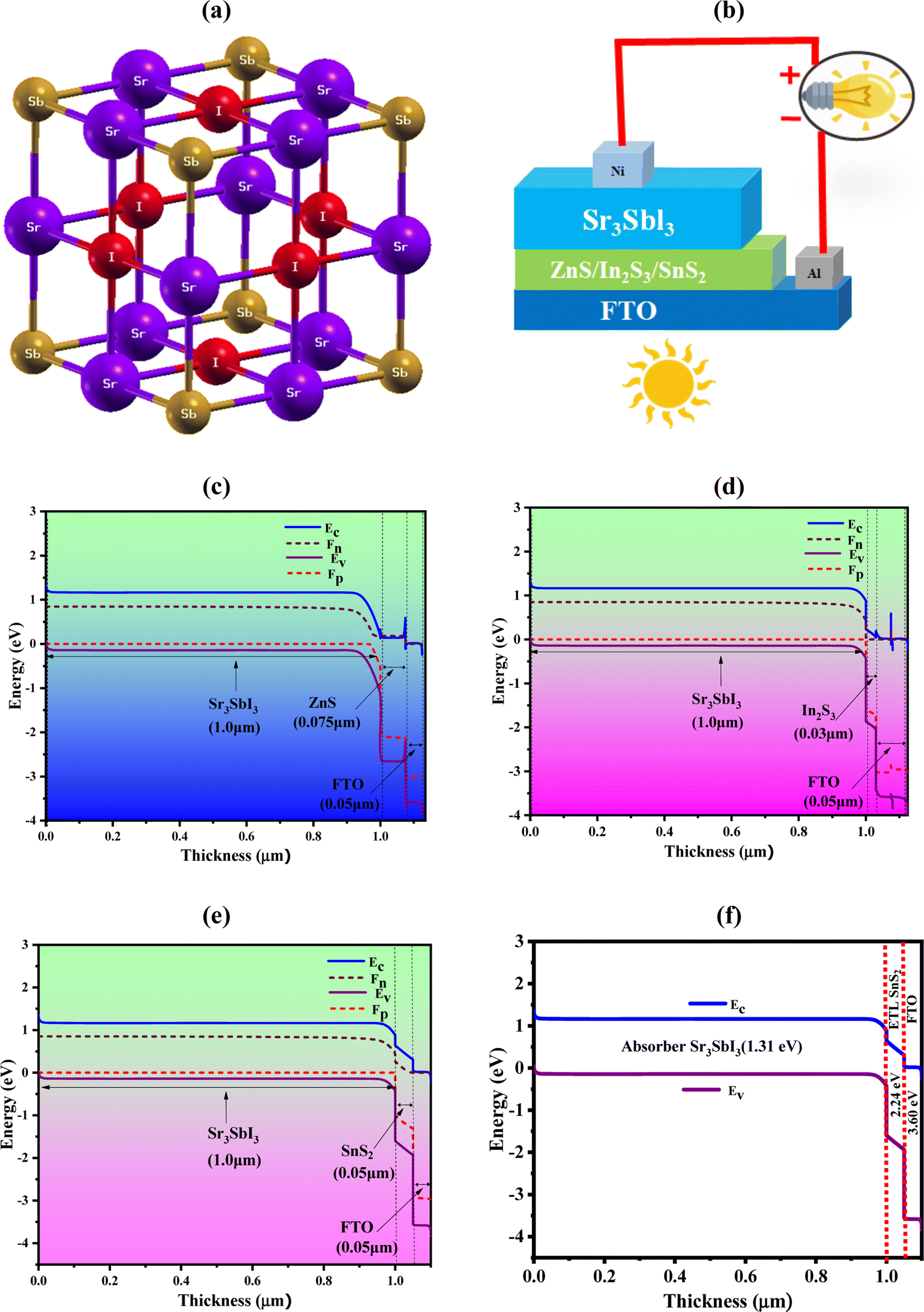
Sr2+ forms an octahedron called SrSb2I4 with two comparable Sb3− and four equivalent I1− atoms as its partners. The angles of the octahedral corner-sharing tilt are between 3 and 4°. The Sr–Sb bond lengths is 3.26 Å long where the Sr–I bond lengths vary from 3.39 to 3.46 Å. The bonding of Sb3− to six equivalent Sr2+ atoms result in the formation of edge sharing SbSr6 octahedra. I1− is coupled to four analogous Sr2+ atoms in a form resembling a rectangular see-saw. The structure's unit cell is made up of seven atoms. The Sb atoms in the crystal lattice are distributed in the 1a Wyckoff sites, while the Sr atoms are concentrated in the center, allocated to the 1b Wyckoff site with the relative coordinates (0, 0, 0), (0.5, 0.5, 0.5). The I atoms are positioned at the face-centered sites (0, 0.5, 0.5) using the third Wyckoff position and normalized coordinates, as shown in Fig. 1 display the (a) crystal structure of Sr3SbI3, (b) device structure, (c) band diagram with ZnS, (d) band diagram with In2S3, (e) band diagram with SnS2, and (f) band alignment of optimized structure (Al/FTO/SnS2/Sr3SbI3/Ni). In order to maintain a mechanically stable lattice while evaluating the energy density function for the lowest energy configuration, a crystal cell parameter must produce an energy minimum level. The lattice constant of our improved relaxed Sr3SbI3 structure is 6.7575 Å. The optimum value agrees with the outcomes of earlier reports.7,8 Additionally, a structure's conjunctive and production energy may be used as effective tools to demonstrate the building's durability,34 with following formula:| | |
EFormation = ESr3SbI3 − ESrI − EAsI2
| (1) |
 |
| | Fig. 1 The (a) crystal structure of Sr3SbI3, (b) device structure, (c) band diagram with ZnS, (d) band diagram with In2S3, (e) band diagram with SnS2, and (f) band alignment of optimized structure (Al/FTO/SnS2/Sr3SbI3/Ni). | |
Herein, the formation energy of Sr3SbI3 is approximately of –1.738 eV per atom (negative). This energy that is negative both conjunctive and formation revealed the stability of Sr3SbI3 structure perovskite structure.
Table 1 is shown the three-device structures. This photovoltaic cell has been simulated using the one-dimensional SCAPS simulator developed at the Electronic and Information Systems Department at the University of Ghent in Belgium. By resolving the fundamental equations of continuity and electrostatic potential under steady-state conditions, it is possible to forecast and analyze the optoelectronic properties of PV cell layouts.35,36 The heterojunction TFSC structure of the device-1 have shown in Fig. 1(b). The suggested PV cell is composed of an FTO window layer, a highly doped n-type SnS2 buffer, and a p-type absorber layer, respectively. And energy band diagram (EBD) for SnS2 shows in Fig. 1(e). Fig. 1(b) also shows the structure of device-II, III where the ZnS and In2S3 as a buffer layer. To understand the carrier dynamics, Fig. 1(c) and (d) illustrate the energy band diagram (EBD) for device-II and III.
Table 1 Three proposed device structures
| Al/FTO/SnS2/Sr3SbI3/Ni |
Device-1 |
| Al/FTO/ZnS/Sr3SbI3/Ni |
Device-2 |
| Al/FTO/In2S3/Sr3SbI3/Ni |
Device-3 |
The generation of electron–hole pairs inside the device is confirmed by the observation of corresponding position of quasi-Fermi levels of Fp and Fn following the illumination. Varied position of the valence band (VB) and conduction band (CB) of the absorber provides evidence of generation of electron–hole pairs. The work function (WF) differential between the absorber and transport layers is the cause of the observed offset. At the absorber/ETL interface, potential inherent and related electric fields aid in separating free electrons from light-generated electrons. Through FTO, a nickel (Ni)-based back electrode, and an aluminum (Al) front electrode, extracted electrons from the ETL are collected significantly in the external circuit. The input data of each simulation parameters are listed in Table 2. The parameters for FTO, In2S3, ZnS, SnS2, and Sr3SbI3 were gathered from published experimental studies and earlier theoretical calculations. As an aid to the numerical study, the thermal velocities of the holes and electrons in each layer have been determined to be 107 cm s−1. The front and back electrodes are composed of nickel (Ni) and aluminum (Al), respectively, with a WF of 5.35 eV (111) and 4.26 eV (100). The ZnS, In2S3 and SnS2, ETLs-based devices structures are named as device-I, II, III photovoltaic cell research employed the interface characteristics listed in Table 3.
Table 2 Input parameters of the FTO, multiple ETL, and absorber layer
| Parameters |
FTO40 |
In2S3 (ref. 43) |
ZnS42 |
SnS2 (ref. 41) |
Sr3SbI3 (ref. 7 and 8) |
| Thickness (nm) |
50 |
30 |
75 |
50 |
1000 |
| Band gap, Eg (eV) |
3.6 |
2.1 |
2.8 |
2.24 |
1.31 |
| Electron affinity, χ (eV) |
4.5 |
4.65 |
3.8 |
4.24 |
4.0 |
| Dielectric permittivity (relative), εr |
10 |
13.5 |
9 |
10 |
5.4 |
| CB effective DOS, NC (1 cm−3) |
2 ×10¹⁸ |
1.8 × 10¹⁹ |
2.2 × 10¹⁸ |
2.2 × 10¹⁸ |
1.2 × 10¹⁹ |
| VB effective DOS, NV (1 cm−3) |
1.8 ×10¹⁹ |
4 × 10¹³ |
1.8 × 10¹⁹ |
1.8 × 10¹⁹ |
2.4 × 10¹⁹ |
| Electron mobility, μn (cm2 V−1 s −1) |
100 |
400 |
100 |
50 |
100 |
| Hole mobility, μh (cm2 V−1 s −1) |
20 |
210 |
25 |
50 |
50 |
| Shallow uniform acceptor density, NA (1 cm−3) |
1 × 10⁶ |
1 × 10⁶ |
1 × 10⁶ |
1 × 10⁶ |
1 ×10¹⁷ |
| Hallow uniform donor density, ND (1 cm−3) |
1 × 10¹⁸ |
1 × 10¹⁶ |
1 × 10¹⁹ |
1 × 10¹⁶ |
1 × 10⁶ |
| Defect density, Nt (1 cm−3) |
1 ×10¹⁴ |
1.7 × 10¹⁶ |
1 × 10¹⁴ |
1 × 10¹⁴ |
1 × 10¹² |
Table 3 Data for interface parameters used in the Sr3SbI3 based solar cell
| Parameter |
Sr3SbI3/SnS2 |
Sr3SbI3/ZnS |
Sr3SbI3/In2S3 |
| Defect type |
Neutral |
Neutral |
Neutral |
| σe (cm2) |
1 × 10¹⁹ |
1 × 10¹⁹ |
1 × 10¹⁹ |
| σh (cm2) |
1 × 10¹⁹ |
1 × 10¹⁹ |
1 × 10¹⁹ |
| Er |
0.6 |
0.6 |
0.6 |
| Total defect density |
1010–1018 |
1010–1018 |
1010–1018 |
| Energetic distribution |
Single |
Single |
Single |
| Working temperature (K) |
275–475 |
275–475 |
275–475 |
3. Electronic and optical properties
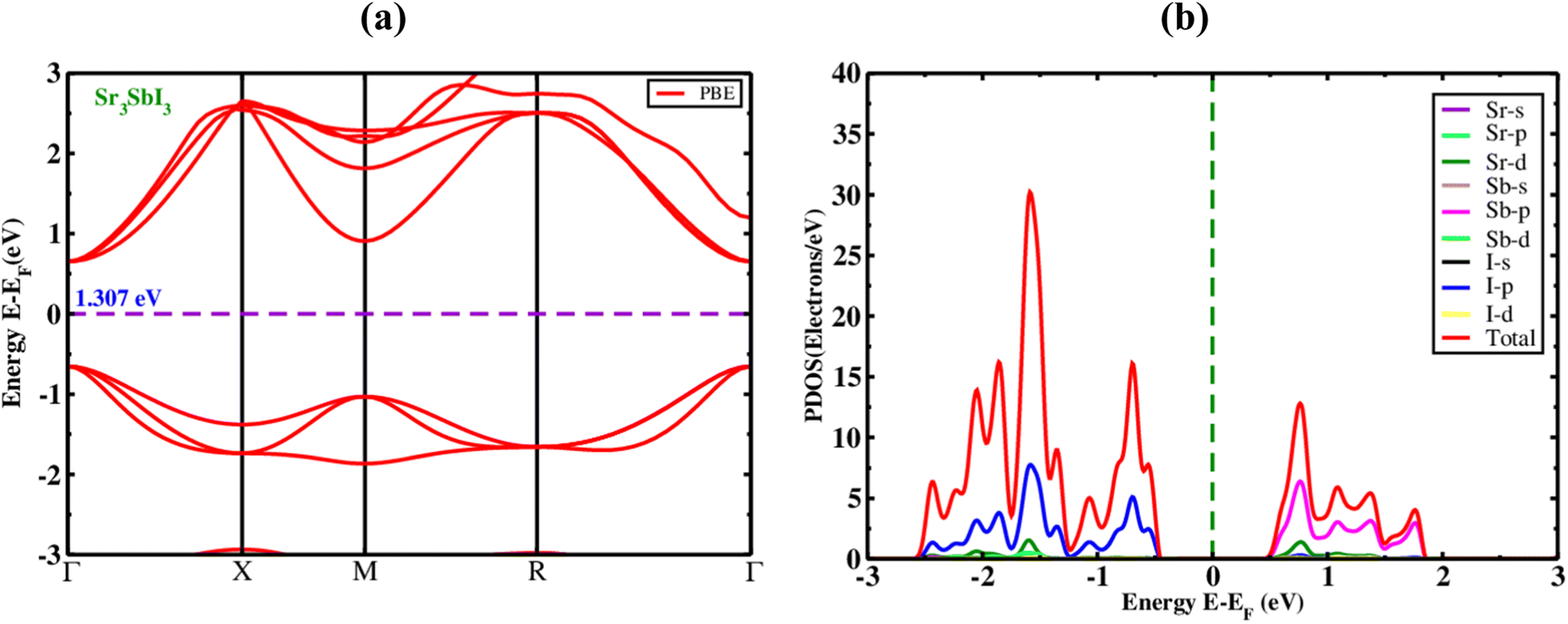
The optical parameters of an inorganic Sr3SbI3 perovskite, the EBS (electronic band structures) of the material were studied. The Sr3SbI3 perovskite structure's electronic optical band gap and evenly spaced orientations were computed. Fig. 2(a) illustrates the generation of Sr3SbI3 perovskite materials, ignoring electronic states above the Fermi level to measure the band gap's overall magnitude.
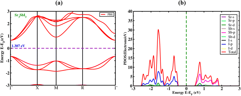 |
| | Fig. 2 The electronic (a) band structure with PBE function, and (b) PDOS of the inorganic perovskite of Sr3SbI3. | |
This figure shows that the Sr3SbI3 perovskites are already assumed to have bandgap-tuned materials with measurements of about 1.31 eV measured with the PBE mechanism for Sr3SbI3 absorber and show the Fig. 2(a). The conduction band minimum (CBM), valence band maximum (VBM), as well as highest occupied energy level, is situated at the elevated invariant gamma-point. The findings of this study are in agreement with those of earlier investigations.7,8 It is obvious that Sr3SbI3-based structures have a wider bandgap, larger atomic size with increased nucleons. The electrostatic attraction between the nucleus and thus the electrons in the highest occupied energy level (HOEL) is reduced. The energy gap between the conduction and valence bands increases as the cohesive energy and electrostatic attraction weaken. This demonstrates a widening of the gap between the conduction and valence bands that made it suitable for use in solar cells based on the energy band gap values found for the achieved bandgap level. To examine the impact of atoms and their various states on the bandgap energy of Sr3SbI3, we estimated the PDOS. The PDOS distribution in Sr3SbI3 over a −4, 4% eV sequence is shown in Fig. 2(b). For Sr3SbI3, the orbitals of strontium and antimony undergo hybridization with I over the whole range. It suggests that the primary type of link between Sr and Sb is covalent. Additionally, for Sr3SbI3, Sr and Sb transferred their electron charge to I and shows the Fig. 2(b).
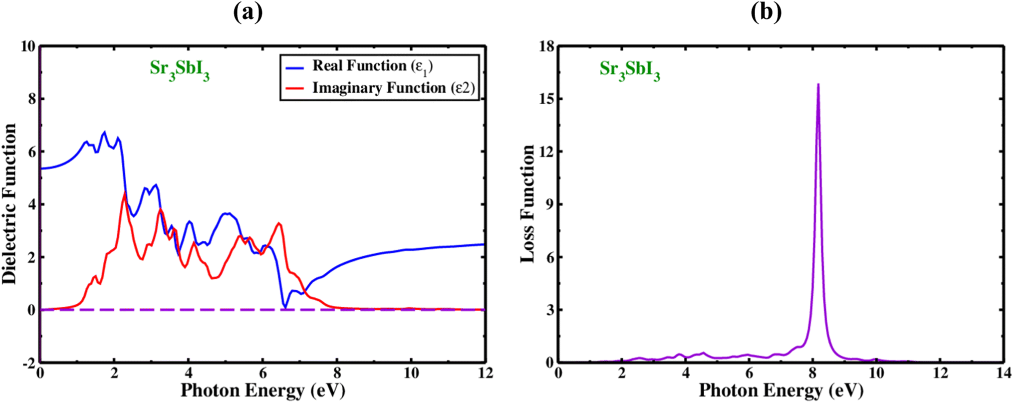
In order to determine whether the materials are appropriate for electronic devices and solar cell technologies, their optical evaluation includes an analysis of the complex dielectric processes, loss of electrons function, absorbance value, and reflectivity. The dielectric functions, which is denoted by the symbol (ω) and shown in Fig. 3(A). It is measured from two components, one of which is actual and is denoted by the sign ε1(ω) and another section is hypothetical, as shown by the sign ε2(ω).
| | |
ε(ω) = ε1(ω) + iε2(ω)
| (2) |
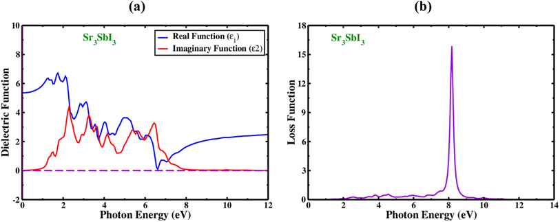 |
| | Fig. 3 (a) The real and imaginary part of the dielectric functions of the inorganic perovskite of Sr3SbI3, and (b) the variation of loss function with photon energy of the inorganic perovskite of Sr3SbI3. | |
The real dielectric functional is computed using Kramers-transformation and Kroning's, while the imaginary area is calculated using momentum matrix elements. Fig. 3(a) display the actual portions of Sr3SbI3's dielectric characteristics at excitation energies as high as 10 eV. The real fraction of the dielectric which is constant can be utilized to determine the effects of polarization and dispersion. The best underlying element in the actual portion of ε1(ω) is the minimal-frequency limit, written as ε1(0), which relates to the circuitry of the real dielectric constant. Cubic Sr3SbI3 has a computed ε1(0) value of 7.55. The quantity of ε1(ω) grew from ε1(0) to the highest value before abruptly reducing, showing the substance's capabilities to absorb light in this spectral range. By varying the biaxial strain, in actual sections of Sr3SbI3 perovskite, the dielectric constant maxima have modified. In comparison to narrow band gap materials, higher bandgap materials often have a lower peak dielectric constant. The energy band gap contracting was increased with compressive stress, resulting in a large dielectric constant peak of the Sr3SbI3 structure with less photocurrent (redshift). The dielectric function of the imaginary part of plays an important role in both the investigation of light absorption and the energy absorption capability of crystal structures due to unbiased charge excitations. For the energy previously measured near to the Fermi level, the imaginary portion of the dielectric function ε2(ω) offers a reliable information on the electronic energy band gap. A sizable section of the absorption zone was filled by Sr3SbI3's ε2(ω) values. These fictional absorption peaks control the migration of the carrier's valence to the conduction band.7,8
Additionally, the hypothetical dielectric fraction of designed system drops to zero when photon energy rises above 4.4 eV. Due to its low optical absorption and higher optical transparency, the material lacks ε2(ω) (over 8.0 eV) transparency. When electrons pass through a dielectric substrate, the amount of energy they lose is referred to as the “electron loss function” that refer how a material reacts to light exposure and is denoted by the sign L(ω). The peak in the plot of L(ω) in Fig. 3(b) for Sr3SbI3 serves as evidence of loss energy, this is found when the energy of the photon surpasses the bandgap of the material. L(ω) = j × ε(ω) − 1. This reflects the visualization of loss function. As shown in Fig. 3(b), the L(ω) peaks for the cubic structure of Sr3SbI3 evolved between 5.0 and 10.0 eV. For Sr3SbI3, the electron loss function that was estimated, L(ω), had a 8.5 eV and it's high value. The energy loss peaks were found to be at energies of 2.5–8.5 eV, respectively. The Sr3SbI3 monolayer would make a good optical solar collector in the infrared and visible spectra because of the existence of L(ω) peaks less than 2.0 eV. It is demonstrated that the photon energies of applied Sr3SbI3 loss function extends up to 10.0 eV.7,8
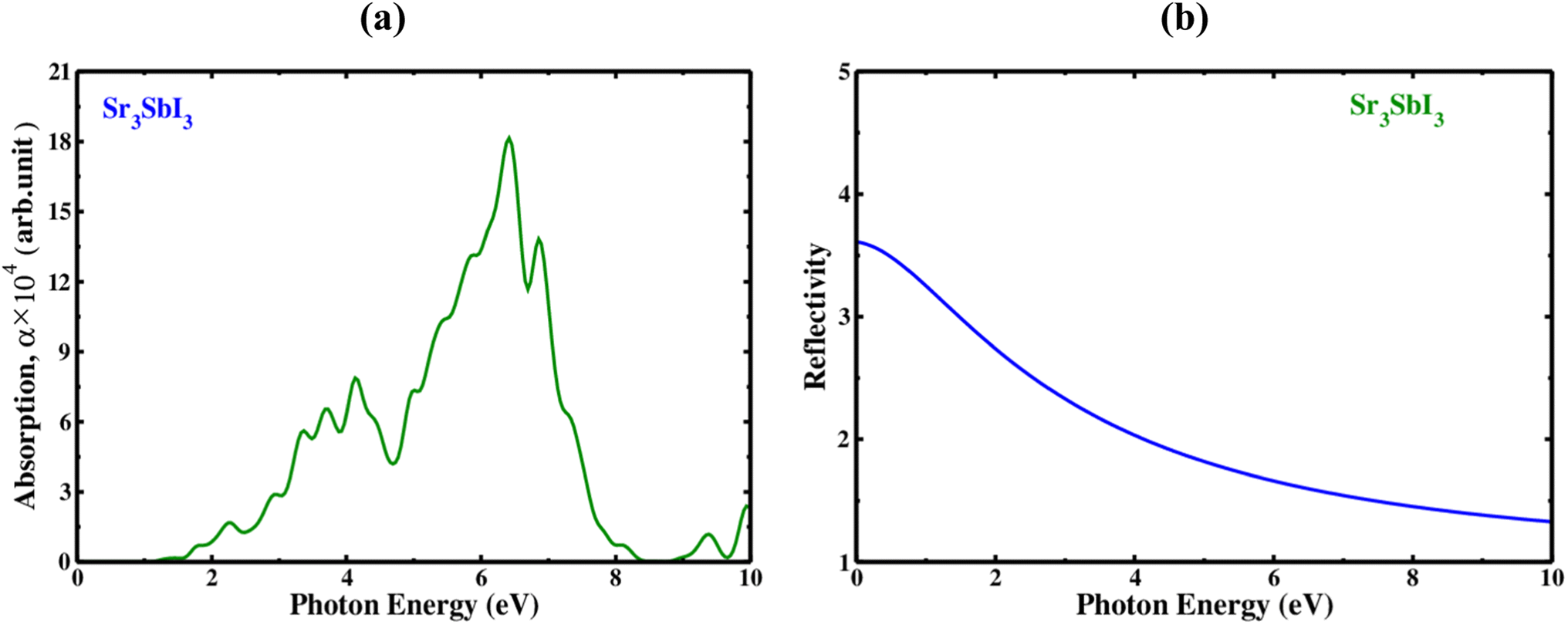
Measured at different wavelengths, the absorption coefficient indicates the degree to which a substance absorbs light, is one important characteristic of Sr3SbI3. An absorption coefficient of Sr3SbI3 perovskite depends on several factors, including the purity of the material, thickness, and crystal structure. The optical absorption coefficient of each configuration displays characteristics similar to the dielectric constant's imaginary part. The visible region of the spectrum of electromagnetic waves often has a higher absorption coefficient since it contains the majority of solar energy. In Fig. 4(a) shows the absorption coefficient of the Sr3SbI3 perovskite material as a measurement of photon energy. In the visible light spectrum, the compressed material absorbs more lights than the tensile structure, which absorbs less light than the unstrained structure. Conventionally, one important consideration is the absorption coefficient for the development of Sr3SbI3 perovskite photovoltaic systems. By raising the absorption coefficient, Sr3SbI3 device's efficiency might be raised, enhancing their ability to compete with other kinds of solar cells.7,8
 |
| | Fig. 4 (a) The absorption spectra with photon energy of the inorganic perovskite of Sr3SbI3, and (b) the reflectivity spectra with photon energy of the inorganic perovskite of Sr3SbI3. | |
Additionally, the incoming light's wavelength and incidence angle may have an impact on the reflectivity of the Sr3SbI3 perovskite. The reflectance of the Sr3SbI3 perovskite material is shown in Fig. 4(b), as a way to quantify photon energy. The largest wide range of reflectance is observed of 0–3.7 eV. This study on Sr3SbI3's optical characteristic is generally in agreement with those from earlier works. Visible light applications benefit more from materials with bandgaps lower than 3.1 eV. The Sr3SbI3 perovskite is a possible contender for using in a multiple of devices; sensors, photodetectors, and solar cells.7,8
4. Simulation methodology
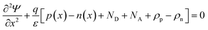
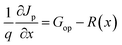
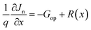
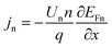
In SCAPS-1D simulator the fundamental equations of one-dimensional semiconductors; Poisson's equation, hole and electron continuity equations as well as the drift and diffusion drift eqn (3)–(7) (ref. 37–40) have solved to determined PV parameters. The Poisson and continuity equations provide a set of coupled differential equations (Ψ, n, p) or (Ψ, EFn, EFp) with correct boundary conditions at interfaces and contacts. In this simulator, the intrinsic properties of each layer such as layer thickness (nm), the band gap Eg (eV), the electron affinity χ (eV), dielectric permittivity, εr, states density of the conduction band NC (cm−3), density of the valence band NV (cm−3), electron mobility μn (cm2 V−1 s−1), hole mobility μp (cm2 V−1 s−1), donor density ND (cm−3), acceptor density NA (cm−3), recombination coefficient (cm3 s−1) radiative recombination, Shockley–Read–Hall recombination (SRH) and Augur recombination, and absorption coefficient, are required to provide from experimental outcomes as well as reported literature. The simulation was performed under AM1.5G standard spectrum. In SCAPS-1D simulator, the absorption coefficient of each photoactive material is required to introduce separately for simulating any structures from experimental finding as summarized in Tables 2 and 3. Herein, the authors collected the validated absorption coefficients of In2S3, ZnS, and SnS2 from literature.41–43
So far, a noticeable discrepancy in theoretical calculation and measured values PV parameters may observe when the suggested device will be fabricated in laboratory mostly owing to the following three factors: (1) photonic loss, (2) electronic loss and (3) instrument loss/measurement errors. The photonic loss includes the absorption loss owing to non-ideal transport layer used in solar cells like transparent conductive layers (TCO), inharmonious interface to transport incident light to absorber layer, and absorber material purities. While, the electronic loss is includes with series and shunt resistances, the material purity and interface quality to transport photogenerated carriers. The instrument loss/measurement errors refer electronic loss during device measurement for associated instrument precession level and wiring for the connections. Additionally, fabrication limitations of the photoactive material, surface properties of thin films, processing of synthesized photoactive films, devices fabrications method and environment impacts are considered as the major hindrance and deviation factors of measures efficiency and theoretically predicted values. Sometimes, an overestimation or overlooking the affecting factors, assuming non-realistic parameters related to interface property, optical loss coefficient, electronic transport properties during simulation may originate a large deviation in cell efficiency in theoretical calculation and those measured by laboratory. However, specifically identification the accurate affecting parameters is still un-solved and open issues.
| |
 | (3) |
| |
 | (4) |
| |
 | (5) |
| |
 | (6) |
| |
 | (7) |
where,
ψ is the electrostatic potential,
ε0εr is the vacuum and semiconductor permittivity,
n and
p are free carrier concentrations, and
N+d and
NA are ionized donor and acceptor densities. The defect charge density is denoted by “
ρdef”,
G is the generation rate, and
jn and
jp are the electron–hole current densities,
q is the elementary charge,
Un and
Up are respectively electron and hole recombination rate,
μn and
μp are electron and hole mobility, respectively.
44,45
In SCAPS-1D simulator, radiative and Auger (band-to-band) recombination introduce according to eqn (8) and (9).46
| | |
Uradiative = K(np − ni2)
| (8) |
| | |
UAuger = (CAnn + CApp)(np − ni2)
| (9) |
The parameters of K, CAn and CAp can be set on the layer panel (for Si, KSi = 1.8 × 10⁻¹⁵ cm−3 s−1 and appropriate values for the Auger constants are: CAn ≈ CAp ≈ 3 × 10⁻³¹ cm−6 s−1).
5. Result and discussion
5.1 Optimization of absorber layer thickness and carrier concentration
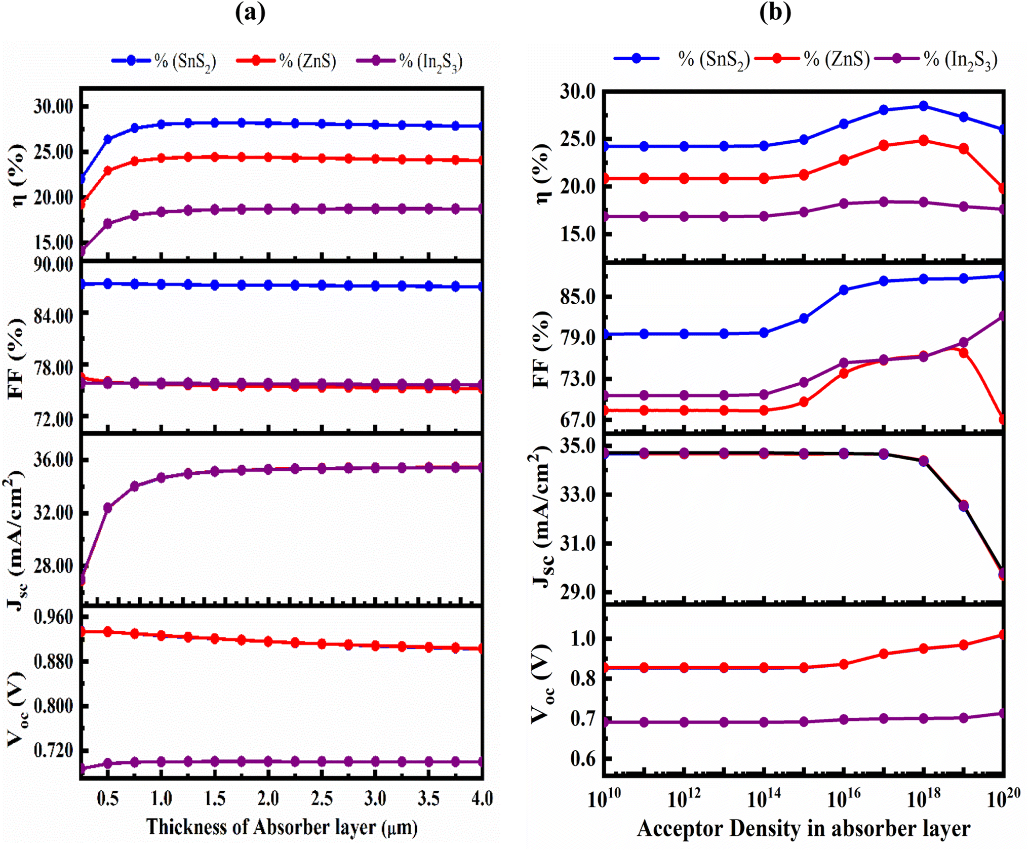
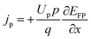
Fig. 5(a) shows the effect of variation in absorber's thickness from 250 to 4000 nm to find out optimize performance of our three simulated devices. The absorber layer's thickness and carrier concentration play a key role in increasing the efficiency of thin-film PV cells. During optimization, as absorber thickness rose, the reverse saturation current increased as well, and for the SnS2 and ZnS ETL, the VOC decreased while it is increased for the In2S3 even in small extent.47 With increasing thickness, spectral reaction will grow at longer wavelengths, hence the JSC increased with the rising thickness48,49 and, it reaches to saturated value. Owing to the increased absorber thickness, the structure displayed different FF drops. The effects of rate of photon absorption and recombination of charge carriers caused the efficiency to decrease without the HTL structures the appropriate absorber thickness on both sides of 1000 nm for ZnS ETL. It slightly decreased for the SnS2 and In2S3-based structures with the increased of absorber thickness.50 A greater number of photons are absorbed as the thickness of the absorber layer increases, while the rate of recombination is also increased. However, the PCE drops and the electrodes carrier extraction is substantial for a narrow absorber as it can only take in a few photons.51,52 A proper balance between light absorption and moving carriers is required because a perovskite layer that is too thick can only convert so much power.53,54 Therefore, the ideal thickness for the Sr3SbI3 absorber in the study was determined to be 1000 nm in order to achieve better performance of VOC of 0.927 V, JSC of 34.67 mA cm−2, FF of 87.3%, and PCE of 28.05% for SnS2, the 0.9269 V, 34.67 mA cm−2, 75.71%, and 24.33% for ZnS ETL, and the 0.7001 V, 34.666 mA cm−2, 75.81%, and 18.4% for In2S3 ETL heterostructure. The performance evaluation's following stage includes this optimization outcome. The acceptor density (NA) of the Sr3SbI3 layer was adjusted from 1010 to 1020 cm−3 to assess the effect of the absorber's NA on the PV characteristics. The variation of FF, PCE, VOC, and JSC depending on the configurations shows in Fig. 5(b). The VOC of the PSC stayed constant at a fixed value during the optimization as increases in the NA.
 |
| | Fig. 5 (a) the impact of the Sr3SbI3 absorber layer's thickness variation and (b) acceptor density variation on PV parameters of VOC, PCE, JSC, and FF. | |
The Fermi energy level of the hole decreases as NA of the absorber layer increases, increasing the VOC as similar in previous report.55 The built-in potential rises with an increase in the absorber layer's NA. The increase in charge separation is another factor for the rise in VOC. The JSC remained constant for all three designs as the density rises up to 1014 cm−3. After exceeding this level, the JSC of the both ETL-structures cell's performance reduced, while the other values remained constant. Both are marginally reduced when the density value is over 1017 cm−3. However, the PCE decreases when the absorber layer's NA value exceeded 1018 cm−3. This may owing to the rising in the number of defect states with increasing acceptor density NA of absorber layer as observed in previous report.56 Table 4 displays a comparative study on PV parameters with different ETLs of In2S3, ZnS and SnS2. The maximum PCE of 28.05 obtained in SnS2/Sr3SbI3 structure PSC.
Table 4 A comparative study on the PV characteristics for different ETLs/Sr3SbI3 heterostructures with a range of ETL and 1017 cm−3 acceptor density
| Parameters |
In2S3 |
ZnS |
SnS2 |
| Thickness (nm) |
50 |
75 |
50 |
| VOC (V) |
0.7001 |
0.9269 |
0.9268 |
| JSC (mA cm−2) |
34.663816 |
34.670126 |
34.668047 |
| FF (%) |
75.87 |
75.71 |
87.3 |
| PCE (%) |
18.41 |
24.33 |
28.05 |
5.2 Optimization of thickness and carrier concentration of ETL layer
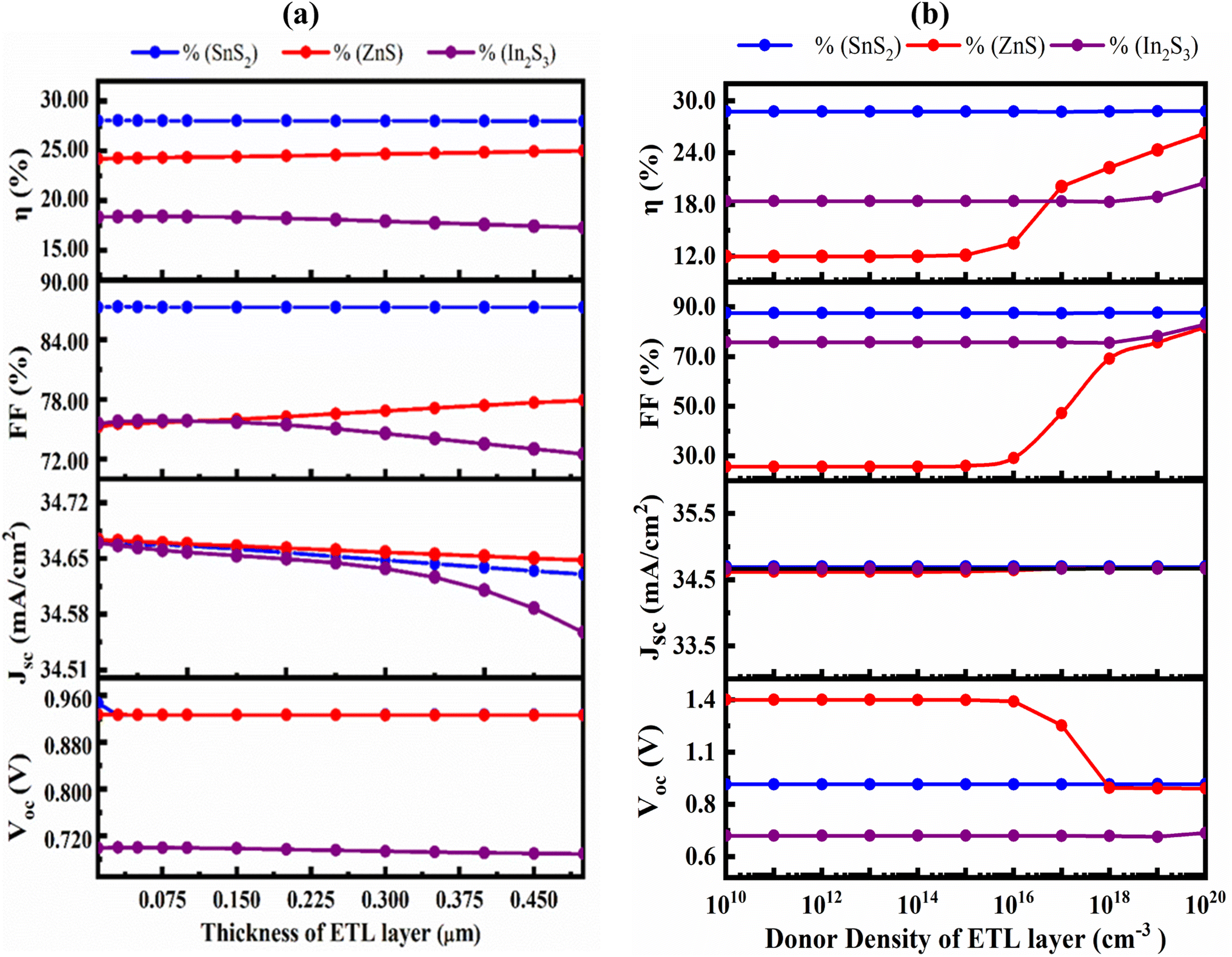
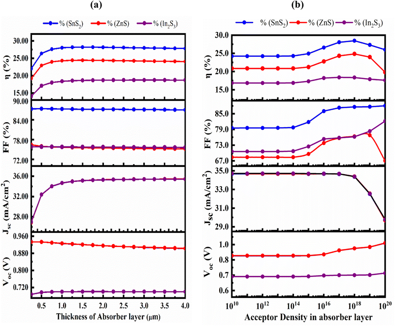
The transmittance of the PSC can be raised with least the recombination currents are lowered with the appropriate ETL.57 In this study, the SnS2, ZnS and In2S3 ETL's thickness was varied from 30 to 500 nm while all other variables remained constant. Fig. 6(a) demonstrates impact of the ETL layer thickness on the PV parameters. With increasing ETL thickness, there was an insignificant change in VOC, FF, PCE and JSC, except FF and PCE of the ZnS. With the exception of ZnS, a thicker ETL light absorbs partially with slowing down the generation and collection rate. Because transmittance declines as the ETL becomes thicker, performance loss severely, which is consistent with prior studies.58–60 The VOC, FF, PCE and JSC decreased from 0.9269 V to 0.9268, 87.35% to 87.29%, 28.07% to 28.01%, and 34.669![[thin space (1/6-em)]](https://www.rsc.org/images/entities/char_2009.gif) 351 mA cm−2 to 34.63035 mA cm−2 respectively for SnS2 ETL. For ZnS the value of VOC and JSC are decreased from 0.9271 V to 0.9267 and 34.67279 mA cm−2 to 34.64807 mA cm−2 but FF and PCE are slightly increased from 75.58% to 77.93%, 24.29% to 25.02%. For In2S3 ETL, the JSC, FF, PCE and VOC both are decreased from 34.66668 mA cm−2 to 34.55731 mA cm−2, 75.81% to 72.53% and 18.4% to 17.28%, respectively. Thus, the optimal ETL thickness of 50, 75 and 50 nm for the SnS2, ZnS and In2S3 ETLs were obtained.
351 mA cm−2 to 34.63035 mA cm−2 respectively for SnS2 ETL. For ZnS the value of VOC and JSC are decreased from 0.9271 V to 0.9267 and 34.67279 mA cm−2 to 34.64807 mA cm−2 but FF and PCE are slightly increased from 75.58% to 77.93%, 24.29% to 25.02%. For In2S3 ETL, the JSC, FF, PCE and VOC both are decreased from 34.66668 mA cm−2 to 34.55731 mA cm−2, 75.81% to 72.53% and 18.4% to 17.28%, respectively. Thus, the optimal ETL thickness of 50, 75 and 50 nm for the SnS2, ZnS and In2S3 ETLs were obtained.
 |
| | Fig. 6 Effect of variation in (a) the ETL layer thickness; (b) carrier concentration on VOC, JSC, FF, and PCE. | |
The variation of the PV characteristics with regard to the doping concentration (ND) for both ETL is shown in Fig. 6(b). The VOC at a SnS2 ETL ND of ≤1016 cm−3 retained at almost unchanged, while it slightly increased to 0.9472 V and the decreased to a 0.9468 V for further increasing from 1018 cm−3 to 1020 cm−3. The JSC and FF both noticeably increased from 34.692332 mA cm−2 to 34.693017 mA cm−2 and 87.61% to 87.73% respectively after that remaining constant up to 1014 cm−3 for JSC and 1015 for FF. For ZnS, the VOC decreased from 1.3505–0.9267 V, JSC increased from 34.62–34.671 mA cm−2, FF gradually increased from 25.64–81.84% and PCE increased from 11.99 to 26.3% when donor density changed from 1010 to 1020 cm−3. For In2S3, for both VOC, JSC, FF and PCE remain constant when donor density varied from 1010–1016 cm−3 and then increased slightly. Device-I with SnS2 ETL found as the best structure at a ND of 1016 cm−3.
5.3 Optimization defect densities of absorber and buffer layer
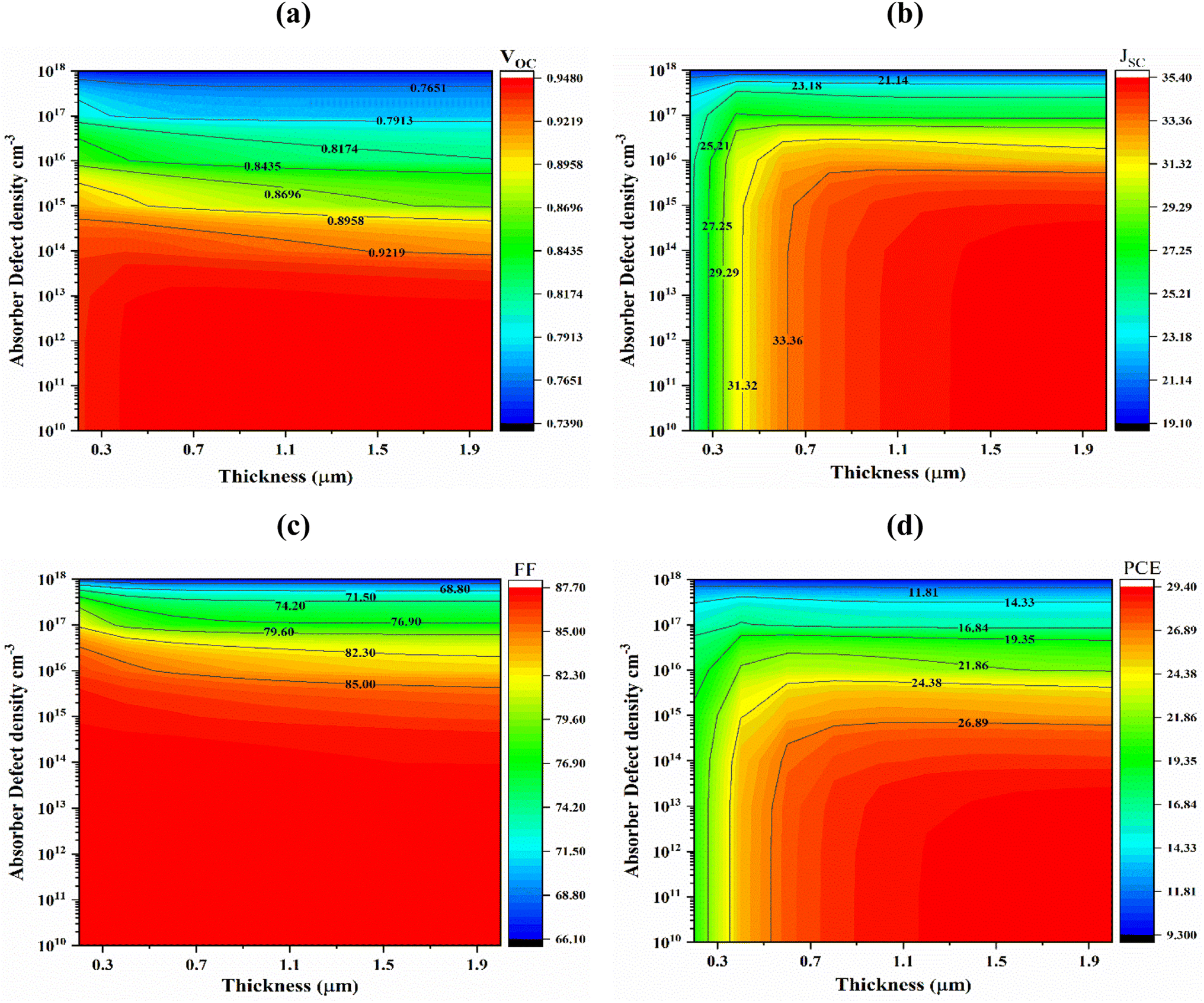
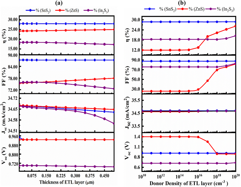
The defect density (Nt) of the absorber has a considerable impact on PSC efficiency. Light interaction with the absorber layer results in the generation of photoelectrons. Fig. 7(a) shows the impact of absorber defect density (Nt) with thickness in the range from 1010 to 1018 cm−3 and 0.2–2.0 μm. When absorber layer thickness 1.0 μm and the bulk defect density were changed from and 1010 to 1018 cm−3, the JSC, VOC, FF, and PCE of cells (Al/FTO/SnS2/Sr3SbI3/Ni) fell from 34.69 to 19.155 mA cm−2, 0.9472 to 0.7398 V, 87.61 to 66.19% and 28.79 to 9.38% respectively. Device carrier recombination, lifespan reduction and performance decline are largely caused by non-radiative recombination of Shockley–Read–Hall (SRH),47 is the major source of this performance decline. When the absorber layer thickness is greater than 1.5 μm and the defect density is less than 1012 cm−3, the VOC, JSC, FF and PCE reaches its maximum value of 0.9478 V, 35.36 mA cm−2, 87.62% and 29.36%, respectively shown in Fig. 7(a)–(d). As a result, at a layer thickness of 1.0 μm and a defect density of 1012 cm−3 the greatest and optimized conversion efficiency 28.78% was achieved considering tradeoff among PV parameters.
 |
| | Fig. 7 Effects of Sr3SbI3 absorber thickness and bulk defect density variations on photovoltaic parameters; (a) VOC (b) JSC (c) FF and (d) PCE. | |
On the other hand, the defect density (Nt) and SnS2 ETL layer thickness affects the structure's performance (Fig. S1a–d†) demonstrates how. The Nt of SnS2 was raised from 1010 to 1018 cm−3 and thickness vary from 50 to 500 nm. The maximum of PV parameters attained at 500 nm and 1010 cm−3 whereas minimum PV parameters attained at 500 nm and 1018 cm−3. The VOC, JSC, FF, and PCE were almost unchanged for same value of Nt due and slightly changed at same thickness for its highly doped metal-like characteristics with thinner thickness as similar tendencies observed in previous report,48 results in the optimized value, Nt of 1014 cm−3 and thickness of 50 nm are selected for the further study.
5.4 Optimization of interface defect densities
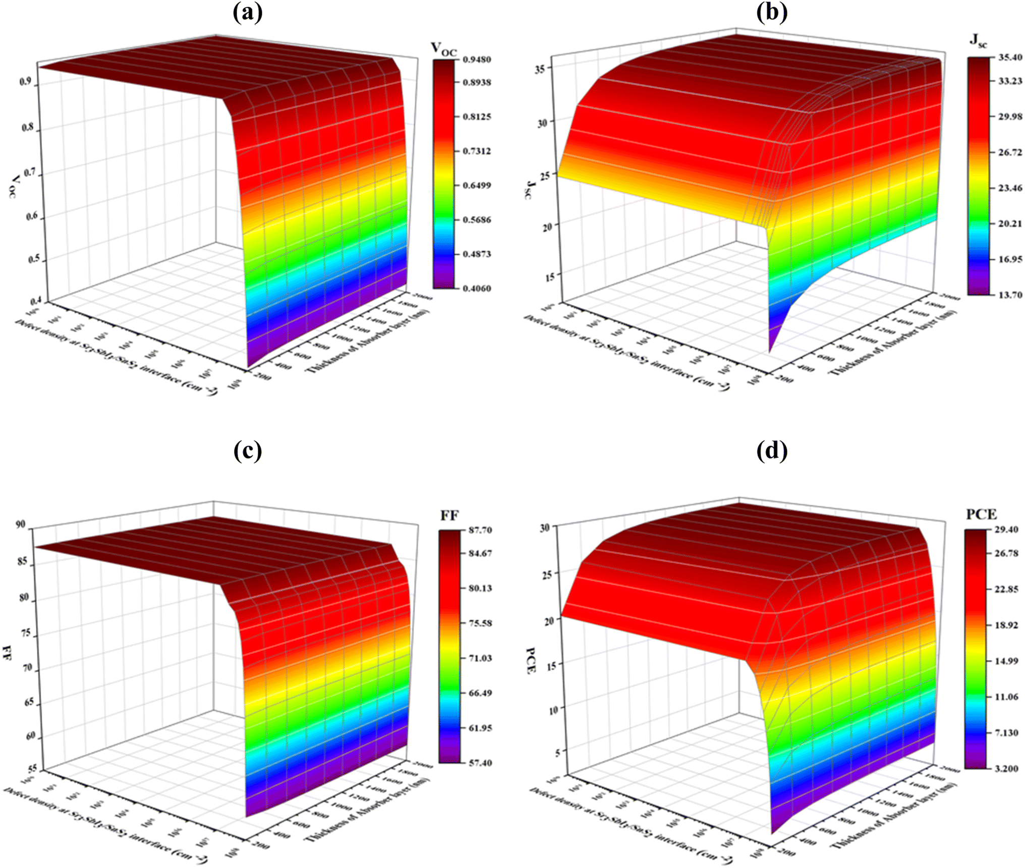
Fig. 8(a)–(d) shows how the PV parameters change when the density of Sr3SbI3/SnS2 interface defects, which ranges from 1010 to 1018 cm−2 is varied. The Sr3SbI3 absorber layer thickness ranges from 200 to 2000 nm. The maximum VOC of 0.9472 V was found at the full Sr3SbI3 thickness when the density of defect was below 1011 cm−2, but it significantly decreased from 0.9472 to 0.4064 V for the defect density above 1016 cm−2 Fig. 8(a). At a defect density of 1010 cm−2 and an absorber thickness of 2000 nm, the maximum value of JSC of 35.36 mA cm−2 was attained at Fig. 8(b).
 |
| | Fig. 8 Effects of thickness of absorber and interface (Sr3SbI3/SnS2) defect density variations on photovoltaic parameters of (a) VOC (b) JSC (c) FF and (d) PCE. | |
As demonstrated in Fig. 9(c), at each specific value of the Sr3SbI3 absorber in the range of 200 to 2000 nm and interface defect density ≥1010 cm−2, the FF steadily dropped from 87.61% to 57.42%. As Fig. 9(d), the defect density of 1010 cm−2 and absorber thickness of 1000 nm led to the greatest converting effectiveness 28.28%. According to the precise modeling results, faults at the Sr3SbI3/SnS2 interface have a much greater negative impact on a solar cell performance than defects at the SnS2/Sr3SbI3/HTL interface, which is in line with published studies.61,62 The interface between Sr3SbI3 and SnS2 must have a defect density of 1010 cm−2 in order for the suggested Sr3SbI3 cell to operate at its best.
 |
| | Fig. 9 (a) J–V and (b) QE curves of the PSC for the best-optimized structure. | |
5.5 Optimized J–V and QE characteristics
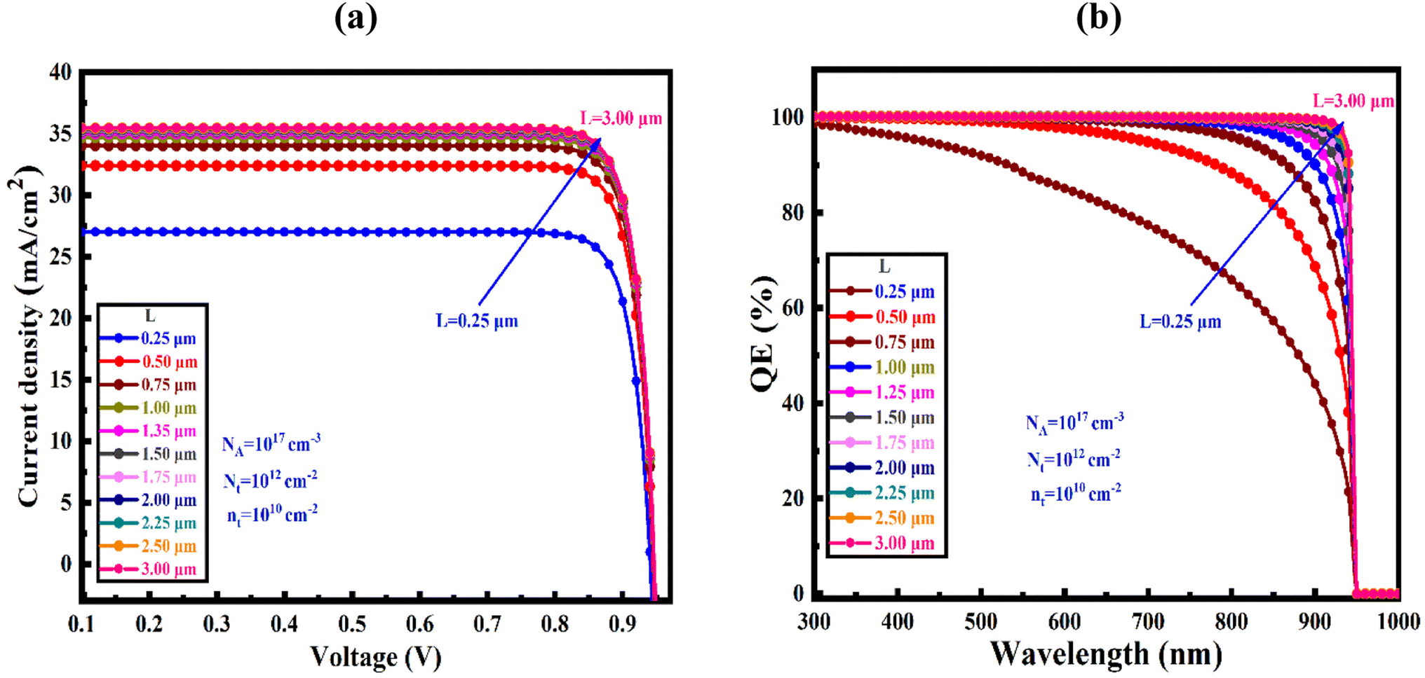
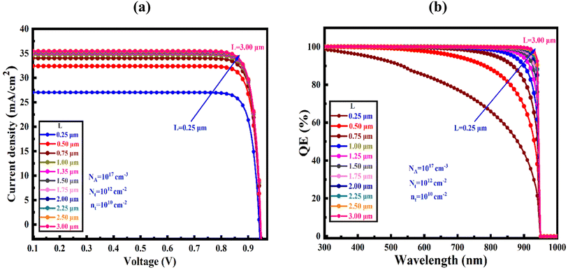
Fig. 9(a) illustrate the device's current density–voltage (J–V) curves for the optimized device-I at varying absorber's thickness of SnS2 changed from 250–4000 nm at a Nt from 1× 10¹⁰ to 1 × 1020 cm−3 and NA from 1 × 10¹⁵ to 1 × 1017 cm−3. The maximum power conversion efficiency (PCE) of 28.05% with JSC of 34.67 μA cm−2, FF of 87.31%, and VOC of 0.93 V for SnS2 ETL, although the PCE have gained of 24.33%, and 18.40% for ZnS and In2S3 ETLs heterostructures, respectively. Previous studies showed that the current density gradually decreased as the voltage increased.63 Fig. 9(b) demonstrates the connection between the optimized device's quantum efficiency (QE) and wavelength. The ratio of charge carriers produced by light to photons striking the solar cell is known as QE.64,65 In the QE curves, wavelengths in the range of 300 to 1000 nm were employed. QE decreased from a starting position of about 100% to 0% at 950 nm, which support the result obtained in J–V characteristics (Table 5).
Table 5 A comparative study on PV parameters of various perovskites
| Perovskites |
VOC (V) |
JSC (mA cm−2) |
FF (%) |
PCE (%) |
Ref. |
| CsPbBr3 |
0.89 |
17.98 |
87.00 |
13.86 |
66 |
| CsPbI3 |
1.00 |
21.08 |
86.60 |
19.10 |
67 |
| CsSnCl3 |
1.04 |
26.23 |
84.31 |
23.10 |
68 |
| CsSnI3 |
0.87 |
33.99 |
83.46 |
24.73 |
3 |
| Sr3SbI3 |
0.93 |
34.67 |
87.31 |
28.05 |
This work |
5.6 Comparative studies on PV parameters of various perovskites
The optical and electrical properties of CsPbBr3, CsPbI3 and Sr3SbI3 are almost similar as reported to date since these entire chosen compound is a potential member in a perovskite materials group.7,28,66 However, the relatively low/insignificance toxication characteristics owing to absence of Pb (ecologically sustainable), versatility in device fabrication and stable behaviour to the exposed moisture, heat, and light of Sr3SbI3 made it more promising and potential to be applied in high efficiency perovskite solar cells over CsPbBr3. Additionally, an enhanced charge transport capabilities, high carrier mobility in Sr3SbI3 compare to CsPbBr3 or CsPbI3, Sr3SbI3 draws a considerable attention for further study on the potentiality of Sr3SbI3 for future stable and efficient photovoltaic devices. However, since the study on Sr3SbI3 and its devices application are still in initial stage, it is hard to emphasis on its betterment, though several theoretical reports revealed huge potentiality exhibiting photoconversion efficiency over 25%.66
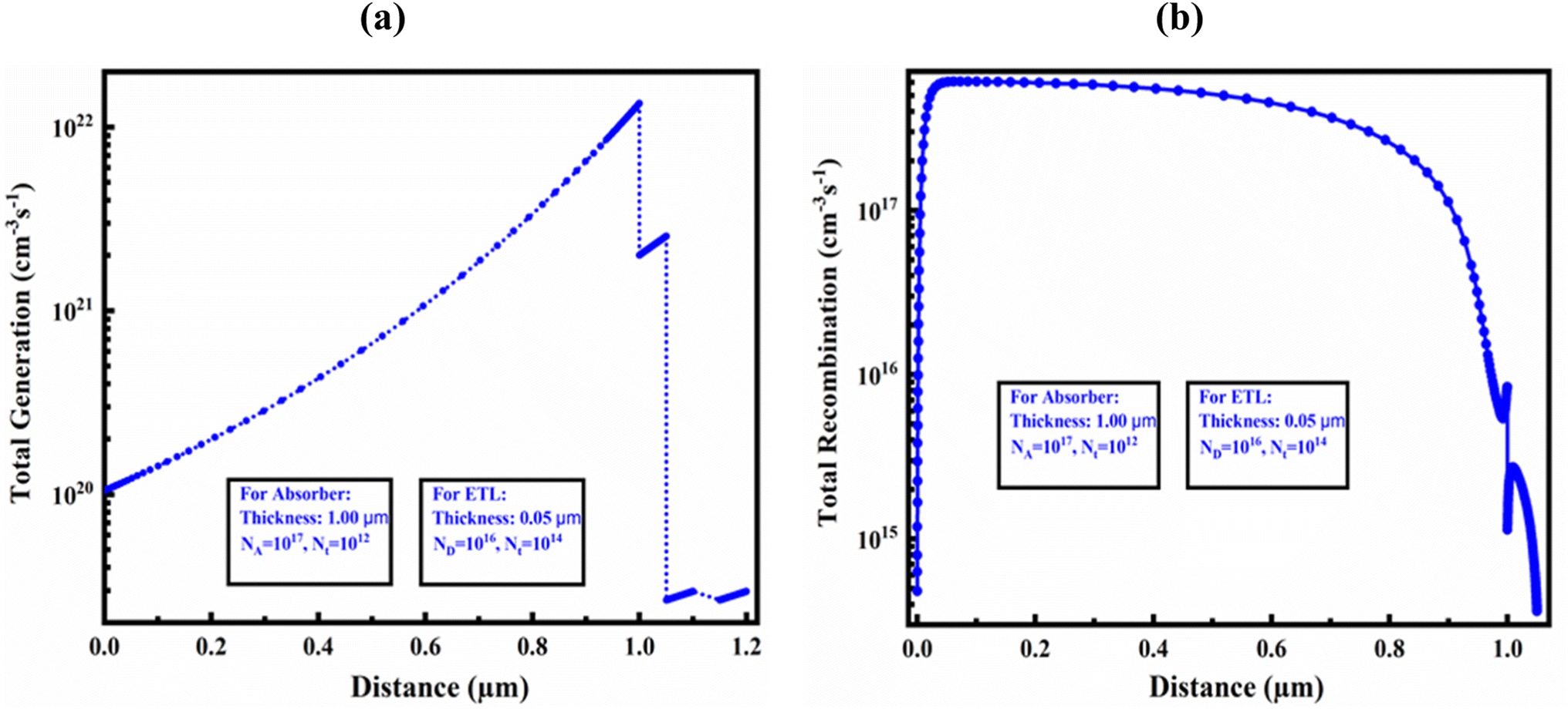
5.7 Analysis of generation and recombination rate
Fig. 10(a) and (b) demonstrate the carrier generation and recombination rate for an optimized structure in the device-I, respectively, corresponding to position. During the carrier generation process, one electron is excited from the VB to CB, leaving a hole in the VB, and this forms electron–hole pairs. These PSCs release electrons and holes, which increases the production of carriers. The highest generating rate was found for the optimized structure at around 1 μm. The generation rate was found the maximum in that area due of the increased photon absorption at that specific region. Nphot (λ, x) SCAPS-1D determines the creation of electron–hole pairs using the incoming photon flux, G(x) can be determined by applying eqn (10):| | |
G(λ, x) = α(λ, x) × Nphot(λ, x)
| (10) |
 |
| | Fig. 10 (a) Photo carrier generation rate and (b) recombination rate in the optimized device structure of Al/FTO/SnS2/Sr3SbI3/Ni structure. | |
The CB's electrons and holes, on the other hand, combine and collapse during the recombination process. The density and duration of the charge carriers impact refer the rate of recombination throughout the designed and optimized PSCs.
Additionally, electron–hole recombination is impacted by the defect state of each PSC layer. This is due to the fact that more electrons in the CB than in other places pass through the energy barrier to travel to the VB, in where they stabilize and occupy a hole's position. Consequently, the energy levels generated at that time had an impact on the electron–hole recombination profile.
The electron and hole carrier concentration are affected by the thickness of Sr3SbI3 absorber layer (Fig. S2a and b†). The effective density of states (DOS) in the valence bands and the Sr3SbI3 hole concentration are caused by the different acceptor concentrations in the absorbers. The electron concentrations are larger than hole concentrations. Predetermined carrier concentration, and compound semiconductor materials utilized as absorber. A similar outcomes was observed in a recent articles.69,70 With lesser e–h recombination and better carrier production obtained in Sr-strontium-based Sr3SbI3 with SnS2 ETL, that made capable as more effective and promising absorber materials to be employed to fabricate high-performance PSC.
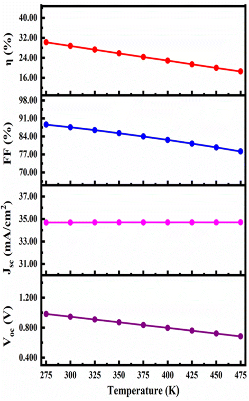
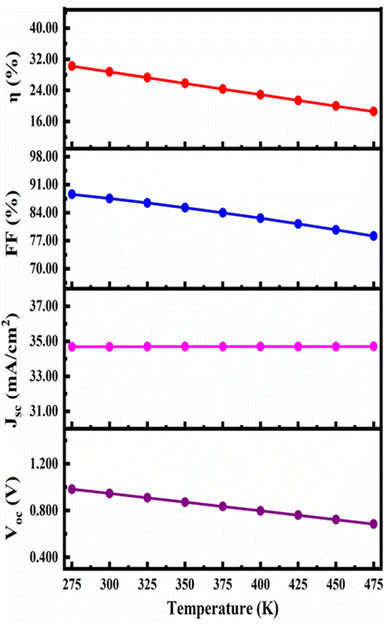
5.8 Effect of cell operating temperature
Fig. 11 demonstrates how the device's properties change as the temperature rises from 275 to 475 K. The JSC, FF, PCE and VOC change from 34.68898 mA cm−2 to 34.70737 mA cm−2, 88.63% to 78.17%, and 30.24% to 18.56% and 0.9835 V to 0.6843 V respectively with increase in working temperature. The device's performance rapidly declined because defects and deformation stress have increased as reported in previous report. Furthermore, temperature rises with the series resistance. RS rises and affects the diffusion length, both of which consequently affect the device's FF and thereby the PCE, which is consistent with reported articles.71,72
 |
| | Fig. 11 Temperature effect on PV solar cell of Al/FTO/SnS2/Sr3SbI3/Ni structure. | |
6. Conclusions
Novel Sr3SbI3-based PSCs showing potential optoelectronic properties and thermal stability studied numerically in details. The optoelectronic parameters of the Sr3SbI3 absorber, with several electron transport layers (ETL: SnS2, ZnS, and In2S3), have been investigated using both of Scaps-1D and DFT study. Subsequently, the photovoltaic (PV) performance of Sr3SbI3 absorber-based cell structures with SnS2, ZnS and In2S3 as ETLs was systematically investigated at varying layer thickness, bulk defect density, doping density, interface density of active materials including working temperature, thereby, optimized PV parameters were achieved. Further, the quantum efficiency (QE), current density–voltage (J–V), and recombination rates were determined to explore the device characteristics. The maximum power conversion efficiency (PCE) of 28.05% with JSC of 34.67 mA cm−2, FF of 87.31% and VOC of 0.93 V for SnS2 ETL was achieved in Al/FTO/SnS2/Sr3SbI3/Ni structure, while the PCE of 24.33%, and 18.40% in ZnS and In2S3 ETLs heterostructures, respectively. The findings of this study contribute to a deep understanding of the physical, electronic, and optical properties of Sr3SbI3 absorber perovskite and SnS2, ZnS, and In2S3 ETLs and provide insights of the strong potential Sr3SbI3 perovskites with S-based ETLs for further experimental design of a high efficiency, green and stable PSC heterostructures.
Abbreviations
| X | Electron affinity |
| μn | Electron mobility |
| μh | Hole mobility |
| BMC | Back metal contact |
| VBO | Valence band offset |
| ND | Shallow uniform donor density |
| BG | Band gap |
| CBO | Conduction band offsets |
| CB | Conduction band |
| SRH | Shockley–read–hall |
| ETL | Electron transport layer |
| PSC | Perovskite solar cell |
| PV | Photovoltaic |
| HTL | Hole transport layer |
| SCAPS | Solar cell capacitance simulator |
| NA | Shallow uniform acceptor density |
| Nt | Defect density |
| JSC | Short circuit current density |
| IE | Ionization energy |
| J–V | Current voltage density |
| PCE | Power conversion efficiency |
| EA | Electron affinity |
| FF | Fill factor |
| ITO | Indium-doped tin oxide |
| EBD | Energy band diagram |
| VOC | Open voltage current |
| VB | Valence band |
| εr | Dielectric permittivity (relative) |
| WF | Work function |
| NC | CB effective density of states |
Data availability
The data that support the findings of this study are available from the corresponding author upon reasonable request.
Author contributions
Md. Ferdous Rahman, Abdul Kuddus: conceptualization, methodology, software, validation, formal analysis, visualization, investigation, data curation, supervision, writing – original draft, review & editing. Md. Shamim Reza: methodology, data curation, software, validation, formal analysis, visualization, investigation, data curation, writing – original draft, review & editing. Md. Rasidul Islam, Mustafa K. A. Mohammed, Ali K. Al-Mousoi, Avijit Ghosh, Sagar Bhattarai, Rahul Pandey, Jaya Madan, M. Khalid Hossain: software, validation, formal analysis, visualization investigation, data curation, review & editing.
Ethical statement
The all authors declare that the manuscript does not have studies on human subjects, human data or tissue, or animals.
Conflicts of interest
The authors have no conflicts of interest.
Acknowledgements
The authors would like to offer their heartfelt appreciation to Dr Marc Burgelman and his colleagues at the EIS Department at the University of Gent in Belgium for providing the opportunity to use the SCAPS-1D software. The authors are also grateful to the Department of Electrical and Electronic Engineering, Begum Rokeya University, Rangpur 5400, Bangladesh, for the use of the Advanced Energy Materials and Solar Cell Research Laboratory.
References
- M. K. Hossain, A. A. Arnab, R. C. Das, K. M. Hossain, M. H. K. Rubel, M. F. Rahman, H. Bencherif, M. E. Emetere, M. K. A. Mohammed and R. Pandey, RSC Adv., 2022, 12, 34850–34873 RSC.
- M. K. Hossain, S. Bhattarai, A. A. Arnab, M. K. A. Mohammed, R. Pandey, H. Ali, F. Rahman, R. Islam, D. P. Samajdar, J. Madan, H. Bencherif, D. K. Dwivedi and M. Amami, RSC Adv., 2023, 13, 21044–21062 RSC.
- M. K. Hossain, M. S. Uddin, G. F. I. Toki, M. K. A. Mohammed, R. Pandey, J. Madan, F. Rahman, R. Islam, S. Bhattarai, H. Bencherif, D. P. Samajdar, M. Amami and D. K. Dwivedi, RSC Adv., 2023, 13, 23514–23537 RSC.
- M. K. Hossain, G. F. I. Toki, J. Madan, R. Pandey, H. Bencherif, M. K. A. Mohammed, M. R. Islam, M. H. K. Rubel, M. F. Rahman, S. Bhattarai and D. P. Samajdar, New J. Chem., 2023, 47, 8602–8624 RSC.
- M. K. Hossain, G. F. I. Toki, I. Alam, R. Pandey, D. P. Samajdar, M. F. Rahman, M. R. Islam, M. H. K. Rubel, H. Bencherif, J. Madan and M. K. A. Mohammed, New J. Chem., 2023, 47, 4801–4817 RSC.
- H. J. Feng and Q. Zhang, Appl. Phys. Lett., 2021, 118, 111902, DOI:10.1063/5.0039936.
- A. Ghosh, F. Rahman, R. Islam and S. Islam, Heliyon, 2023, 9, e19271 CrossRef CAS PubMed.
- F. Rahman, H. Rahman, R. Islam and M. K. Hossain, J. Mater. Sci., 2023, 58, 13100–13117, DOI:10.1007/s10853-023-08825-5.
- A. B. Shanto, F. Rahman, R. Islam, A. Ghosh, A. Azzouz-rached, H. Albalawi and Q. Mahmood, F1000Research, 2023, 12, 1005, DOI:10.12688/f1000research.137044.1.
- M. K. Hossain, D. P. Samajdar, R. C. Das, A. A. Arnab, M. F. Rahman, M. H. K. Rubel, M. R. Islam, H. Bencherif, R. Pandey, J. Madan and M. K. A. Mohammed, Energy Fuels, 2023, 37, 3957–3979, DOI:10.1021/acs.energyfuels.3c00181.
- M. K. Hossain, G. F. Ishraque Toki, D. P. Samajdar, M. H. K. Rubel, M. Mushtaq, Md. R. Islam, Md. F. Rahman, S. Bhattarai, H. Bencherif, M. K. A. Mohammed, R. Pandey and J. Madan, Energy Fuels, 2023, 7380–7400 CrossRef CAS.
- S. Bhattarai, M. K. Hossain, R. Pandey, J. Madan, D. P. Samajdar, M. F. Rahman, M. Z. Ansari and M. Amami, Energy Fuels, 2023, 37, 10631–10641, DOI:10.1021/acs.energyfuels.3c01659.
- M. K. Hossain, M. K. A. Mohammed, R. Pandey, A. A. Arnab, M. H. K. Rubel, K. M. Hossain, M. H. Ali, M. F. Rahman, H. Bencherif, J. Madan, M. R. Islam, D. P. Samajdar and S. Bhattarai, Energy Fuels, 2023, 37, 6078–6098 CrossRef CAS.
- M. K. Hossain, et al., Energy Fuels, 2023, 37, 13377–13396 CrossRef CAS.
- Q. Wang, X. Zhang, Z. Jin, J. Zhang, Z. Gao, Y. Li and S. F. Liu, ACS Energy Lett., 2017, 2, 1479–1486 CrossRef CAS.
- M. K. Hossain, G. F. I. Toki, A. Kuddus, M. H. K. Rubel, M. M. Hossain, H. Bencherif, M. F. Rahman, M. R. Islam and M. Mushtaq, Sci. Rep., 2023, 13, 1–24 CrossRef PubMed.
- K. Wang, Z. Jin, L. Liang, H. Bian, D. Bai, H. Wang, J. Zhang, Q. Wang and S. Liu, Nat. Commun., 2018, 9, 4544 CrossRef PubMed.
- Y. Wang, T. Zhang, M. Kan and Y. Zhao, J. Am. Chem. Soc., 2018, 140, 12345–12348 CrossRef CAS PubMed.
- Y. Wang, X. Liu, T. Zhang, X. Wang, M. Kan, J. Shi and Y. Zhao, Angew. Chem., 2019, 131, 16844–16849 CrossRef.
- T. Zhang, M. I. Dar, G. Li, F. Xu, N. Guo, M. Grätzel and Y. Zhao, Sci. Adv., 2017, 3, e1700841, DOI:10.1126/sciadv.1700841.
- B. Li, Y. Zhang, L. Fu, T. Yu, S. Zhou, L. Zhang and L. Yin, Nat. Commun., 2018, 9, 1076 CrossRef PubMed.
- M. Cha, P. Da, J. Wang, W. Wang, Z. Chen, F. Xiu, G. Zheng and Z.-S. Wang, J. Am. Chem. Soc., 2016, 138, 8581–8587 CrossRef CAS PubMed.
- E. M. Sanehira, A. R. Marshall, J. A. Christians, S. P. Harvey, P. N. Ciesielski, L. M. Wheeler, P. Schulz, L. Y. Lin, M. C. Beard and J. M. Luther, Sci. Adv., 2017, 3, eaao4204, DOI:10.1126/sciadv.aao4204.
- J. Liang, Z. Liu, L. Qiu, Z. Hawash, L. Meng, Z. Wu, Y. Jiang, L. K. Ono and Y. Qi, Adv. Energy Mater., 2018, 8, 1800504 CrossRef.
- H. Zhou, Q. Chen, G. Li, S. Luo, S. Tze-bing, H.-S. Duan, Z. Hong and Y. Yang, Science, 2014, 345, 535–542 CrossRef PubMed.
- S. Li, P. Zhang, Y. Wang, H. Sarvari, D. Liu, J. Wu, Y. Yang, Z. Wang and Z. D. Chen, Nano Res., 2017, 10, 1092–1103 CrossRef CAS.
- B. C. Vasilev, Enhancing the Performance of a Record- Breaking Perovskite/Silicon Tandem Solar Cell, 2021, pp. 1–8 Search PubMed.
- Z. M. Elqahtani, S. Aman, S. Mehmood, Z. Ali, A. Hussanan, N. Ahmad, S. Alomairy, M. S. Al-Buriahi, Z. A. Alrowaili and H. M. T. Farid, J. Taibah Univ. Sci., 2022, 16, 660–669 CrossRef.
- M. F. Rahman, M. A. Rahman, M. R. Islam, A. Ghosh, M. A. Bashar Shanto, M. Chowdhury, M. Al Ijajul Islam, M. H. Rahman, M. K. Hossain and M. A. Islam, AIP Adv., 2023, 13, 085329, DOI:10.1063/5.0156961.
- A. Ghosh, M. F. Rahman, M. R. Islam, M. S. Islam, M. Hossain, S. Bhattarai, R. panday, J. Madan, M. A. Rahman and A. B. Ismail, Opt. Continuum, 2023, 2, 2145, DOI:10.1364/optcon.495816.
- F. Rahman, M. Islam, R. Islam, A. Ghosh and Q. Mahmood, J. Solid State Chem., 2023, 328, 124341 CrossRef.
- F. Rahman, Nano Select., 2023, 1–14 Search PubMed.
- F. Rahman, R. Islam and A. Ghosh, Phys. Scr., 2023, 98, 115105 CrossRef.
- T. Li, C. He and W. Zhang, J. Energy Chem., 2021, 52, 121–129 CrossRef CAS.
- M. Burgelman, P. Nollet and S. Degrave, Thin Solid Films, 2000, 361–362, 527–532 CrossRef CAS.
- M. H. Ali, M. A. Al Mamun, M. D. Haque, M. F. Rahman, M. K. Hossain, A. Z. Md and T. Islam, ACS Omega, 2023, 8, 7017–7029 CrossRef CAS PubMed.
- M. S. Chowdhury, S. A. Shahahmadi, P. Chelvanathan, S. K. Tiong, N. Amin, K. Techato, N. Nuthammachot, T. Chowdhury and M. Suklueng, Results Phys., 2020, 16, 102839 CrossRef.
- A. Ait Abdelkadir, E. Oublal, M. Sahal and A. Gibaud, Results Opt., 2022, 8, 100257, DOI:10.1016/j.rio.2022.100257.
- S. Ahmmed, A. Aktar, M. F. Rahman, J. Hossain and A. B. M. Ismail, Optik, 2020, 223, 165625 CrossRef CAS.
- A. Kuddus, M. F. Rahman, S. Ahmmed, J. Hossain and A. B. M. Ismail, Superlattices Microstruct., 2019, 132, 106168, DOI:10.1016/j.spmi.2019.106168.
- M. A. Ghebouli, B. Ghebouli, R. Larbi, T. Chihi and M. Fatmi, Optik, 2021, 241, 166203 CrossRef CAS.
- Y. Khaaissa, A. Talbi, K. Nouneh, O. El Khouja, H. Ahmoum, A. C. Galca, A. Belahmar, G. Li and Q. Wang, Opt. Quantum Electron., 2021, 53, 487 CrossRef CAS.
- N. Khoshsirat and N. A. Md Yunus, J. Electron. Mater., 2016, 45, 5721–5727 CrossRef CAS.
- A. Thakur, D. Singh and S. Kaur Gill, Mater. Today: Proc., 2022, 71, 195–201 CAS.
- R. Pandey, A. Khanna, K. Singh, S. K. Patel, H. Singh and J. Madan, Sol. Energy, 2020, 207, 893–902 CrossRef CAS.
- J. Al Mahmud, M. F. Rahman, A. Kuddus, M. H. Ali, M. S. Islam, M. D. Haque, S. R. Al Ahmed, M. Mushtaq and A. B. M. Ismail, Energy Adv., 2023, 19–21 Search PubMed.
- I. Alam, R. Mollick and M. A. Ashraf, Phys. B, 2021, 618, 413187 CrossRef CAS.
- U. Mandadapu, Indian J. Sci. Technol., 2017, 10, 1–8 CrossRef.
- M. M. A. Moon, M. F. Rahman, M. Kamruzzaman, J. Hossain and A. B. M. Ismail, Energy Rep., 2021, 7, 1742–1756 CrossRef.
- L. Lin, L. Jiang, P. Li, B. Fan and Y. Qiu, J. Phys. Chem. Solids, 2019, 124, 205–211 CrossRef CAS.
- A. Bag, R. Radhakrishnan, R. Nekovei and R. Jeyakumar, Sol. Energy, 2020, 196, 177–182 CrossRef CAS.
- T. Dureja, A. Garg, S. Bhalla, D. Bhutani and A. Khanna, Mater. Today: Proc., 2022, 71, 239–242 CAS.
- D. Liu, M. K. Gangishetty and T. L. Kelly, J. Mater. Chem. A, 2014, 2, 19873–19881 RSC.
- D. E. Tareq, S. M. AbdulAlmohsin and H. H. Waried, IOP Conf. Ser.: Mater. Sci. Eng., 2020, 928, 072044 CAS.
- P. K. Patel, Sci. Rep., 2021, 11, 3082 CrossRef CAS PubMed.
- K. D. Jayan and V. Sebastian, Semicond. Sci. Technol., 2021, 36, 065010 CrossRef CAS.
- A. Tara, V. Bharti, S. Sharma and R. Gupta, Opt. Mater., 2021, 119, 111362 CrossRef CAS.
- Y. Raoui, H. Ez-Zahraouy, N. Tahiri, O. El Bounagui, S. Ahmad and S. Kazim, Sol. Energy, 2019, 193, 948–955 CrossRef CAS.
- M. M. Salah, M. Abouelatta, A. Shaker, K. M. Hassan and A. Saeed, Semicond. Sci. Technol., 2019, 34, 115009 CrossRef CAS.
- R. Pandey, A. Khanna, K. Singh, S. K. Patel, H. Singh and J. Madan, Sol. Energy, 2020, 207, 893–902 CrossRef CAS.
- S. R. Al Ahmed, A. Sunny and S. Rahman, Sol. Energy Mater. Sol. Cells, 2021, 221, 110919 CrossRef.
- Y. Cao, X. Zhu, H. Chen, X. Zhang, J. Zhouc, Z. Hu and J. Pang, Sol. Energy Mater. Sol. Cells, 2019, 200, 109945 CrossRef CAS.
- G. E. Eperon, G. M. Paternò, R. J. Sutton, A. Zampetti, A. A. Haghighirad, F. Cacialli and H. J. Snaith, J. Mater. Chem. A, 2015, 3, 19688–19695 RSC.
- P. Khan, T. Mahmood, K. Ayub, S. Tabassum and M. Amjad Gilani, Opt Laser. Technol., 2021, 142, 107231 CrossRef CAS.
- M. M. A. Moon, M. H. Ali, M. F. Rahman, A. Kuddus, J. Hossain and A. B. M. Ismail, Phys. Scr., 2020, 95, 035506 CrossRef CAS.
- H.-J. Feng and Q. Zhang, Appl. Phys. Lett., 2021, 118, 111902 CrossRef CAS.
- M. K. Hossain, G. F. I. Toki, I. Alam, R. Pandey, D. P. Samajdar, M. F. Rahman, M. R. Islam, M. H. K. Rubel, H. Bencherif, J. Madan and M. K. A. Mohammed, New J. Chem., 2023, 47, 4801–4817 RSC.
- M. K. Hossain, G. F. I. Toki, A. Kuddus, M. K. A. Mohammed, R. Pandey, J. Madan, S. Bhattarai, M. F. Rahman, D. K. Dwivedi, M. Amami, H. Bencherif and D. P. Samajdar, Mater. Chem. Phys., 2023, 308, 128281 CrossRef CAS.
- Y. Zhou and A. Gray-Weale, Phys. Chem. Chem. Phys., 2016, 18, 4476–4486 RSC.
- O. Ahmad, A. Rashid, M. W. Ahmed, M. F. Nasir and I. Qasim, Opt. Mater., 2021, 117, 111105 CrossRef CAS.
- F. Behrouznejad, S. Shahbazi, N. Taghavinia, H.-P. Wu and E. Wei-Guang Diau, J. Mater. Chem. A, 2016, 4, 13488–13498 RSC.
- S. R. Raga, E. M. Barea and F. Fabregat-Santiago, J. Phys. Chem. Lett., 2012, 3, 1629–1634 CrossRef CAS PubMed.
|
| This journal is © The Royal Society of Chemistry 2023 |
Click here to see how this site uses Cookies. View our privacy policy here. 
 Open Access Article
 This Open Access Article is licensed under a Creative Commons Attribution-Non Commercial 3.0 Unported Licence
 *a,
Abdul Kuddus
*a,
Abdul Kuddus