
 Open Access Article
 This Open Access Article is licensed under a Creative Commons Attribution-Non Commercial 3.0 Unported Licence
Polarization enhanced photoresponse of InSe via 2D ferroelectric CuCrP2S6†
Xiaoliang Weng ,
Lu Qi,
Wei Tang,
Muhammad Ahsan Iqbal,
Chenxu Kang,
Kewen Wu and
Yu-Jia Zeng*
,
Lu Qi,
Wei Tang,
Muhammad Ahsan Iqbal,
Chenxu Kang,
Kewen Wu and
Yu-Jia Zeng*
Key Laboratory of Optoelectronic Devices and Systems of Ministry of Education and Guangdong Province, College of Physics and Optoelectronic Engineering, Shenzhen University, Shenzhen 518060, P. R. China. E-mail: yjzeng@szu.edu.cn
First published on 16th November 2023
Abstract
Two-dimensional CuCrP2S6 possesses significant potential for low-power non-volatile devices owing to its multiferroic properties. Nonetheless, comprehensive investigations regarding the modulation of CuCrP2S6 polarization for enhancing semiconductor photodetection capabilities and its potential applications in ferroelectric non-volatile devices are still relatively scarce. In this study, we present a novel, non-volatile, tunable photodetector engineered through the integration of a ferroelectric heterostructure comprising CuCrP2S6 and InSe. Our findings reveal that distinct ferroelectric polarization states of CuCrP2S6 exert varying modulation effects on the InSe photodetection performance. Notably, optimized results give a responsivity of 1839 A W−1 and a detectivity of 1.9 × 10¹² Jones at a 300 nm wavelength, featuring a substantial 20.7-fold difference in responsivity between the two polarization states. This investigation underscores the immense potential of CuCrP2S6 in the development of non-volatile, multi-state optoelectronic devices.
Introduction
Two-dimensional van der Waals layered (2D vdW) materials have unique physical properties compared to their traditional 3D counterparts.1,2 Among various 2D vdW semiconductors, InSe has excellent performance in optoelectronics owing to its high electron mobility, high light absorption coefficient, and tunable bandgap.3–5 As recently reported, broad spectrum (200–800 nm) and high responsivity (4.9 × 10⁶ A W−1) photodetectors were obtained by building β-InSe and graphene heterostructures combined with photogating effects.6 More InSe-based studies, such as those on the replacement of electrode metals,7 ion doping,8 and compounding with quantum dots,9,10 have confirmed great potential in the field of photodetection.Typical strategies to enhance photoresponse include homo/heterojunction induced built-in field,11–13 gate-induced electrostatic field,14 polarization induced piezo/ferroelectric field,15–17 plasmonics induced localized optical field,18 etc. Ferroelectric modulation holds great promise due to its various inherent advantages, including simplified device fabrication and non-volatility. Notably, there is no need for an external bias to maintain the ferroelectric polarization.17,19,20 Several ferroelectric materials have been used in ferroelectric-enhanced photodetectors; such as HfO2,21 P(VDF-TrFE),22 PZT.23 In contrast, few studies are accessible on ferroelectric-enhanced photodetectors based on 2D ferroelectric materials. Just as ferroelectric polarization and photoexcitation in α-In2Se3/Si junctions can be mutually modulated,24 CuInP2S6/MoTe2 device tunable optical response is non-volatile,25 etc. CuCrP2S6 (CCPS) is an emerging multiferroic candidate, in which the ferromagnetic and ferroelectric polarization are derived from Cr and Cu atoms, respectively.26,27 In particular, ferroelectric behavior at room temperature was predicted by first-principles calculations and confirmed by observation with piezoresponse force microscopy.28,29 However, to the best of our knowledge, the modulation of semiconductor optoelectronic performance using CCPS ferroelectrics has not yet been demonstrated.
In this research, we have successfully engineered photodetectors with a bilayer structure composed of InSe and CCPS. Through the lateral (in-plane) migration of Cu ions, we have effectively induced a polarization field, which, in turn, profoundly influences the photoelectric properties of InSe. Remarkably, not only does this result in an enhancement of InSe's photoelectric response, but it also establishes the non-volatile nature of the polarization state. Additionally, it is noteworthy that the photoresponse modulation varies depending on the incident wavelengths. This study offers a groundbreaking approach to harnessing CCPS polarization in photodetectors, thereby showcasing its tremendous potential in the realm of non-volatile optoelectronic devices.
Experimental
The CCPS and InSe nanoflakes were prepared by mechanical exfoliation from high-quality bulk single crystal (purity of 99.999%, HQ graphene company). We employed a dry transfer technique to fabricate CCPS/InSe heterostructures. First, the block crystals were mechanically peeled off using adhesive tape. Then, the flakes were selected and picked up with polydimethylsiloxane (PDMS, the thickness is 6mil, Prmat company). Subsequently, these selected CCPS and InSe flakes were successively stacked on a Si wafer with a 300 nm SiO2 layer using a homemade alignment transfer system. Stripping and transfer were performed under ambient conditions, and the entire operation took no more than one hour. After that, the designed heterostructures were spin-coated with poly(methyl methacrylate) (PMMA, Allresist company) resist, and then all samples were baked for 5 min at 180 °C. The metal electrodes were obtained using an electron beam lithography (EBL, Raith Pioneer Two, electron beam voltage of 10 kV and an aperture size of 60 μm) process. Subsequently, a magnetron sputtering deposition technique was employed to deposit 5 nm of Ti and 45 nm of Au, carried out at room temperature and under an argon atmosphere at a pressure of 0.5 Pa.The thicknesses of devices were extracted from the atomic force microscopy (AFM) measurements using an AIST-NT SmartSPM. Piezoresponse force microscopy (PFM) was performed using a commercial atomic force microscope (Asylum Research MFP-3D). Bruker D8 ADVANCE was used for X-ray diffraction (XRD) for structural and phase characterization. The molecular vibrational modes were probed using Raman spectroscopy in a Horiba (WITec alpha300R) with a 532 nm excitation laser. A Keysight 4200 A probe station was used to measure the device's electrical properties. The Zolix 500W Xenon Light Source (GLORIA-X500A) was used to study the photoresponse performance of the devices. The power density was calibrated by the power meter (Newport 1919-R).
Results and discussion
The schematic structure of the device is shown in Fig. 1(a). Fig. 1(b) shows the AFM topography of the device. The thicknesses of CCPS and InSe are approximately 52.0 nm and 31.7 nm, respectively. Fig. S1† (ESI) shows the SEM image of the device with the electrodes, in which electrodes 1 and 3 are on the CCPS, and electrodes 2 and 4 are on the InSe. The crystal structures of InSe and CCPS were characterized by using XRD. All the diffraction peaks in Fig. 1(c) correspond to the Bragg position of InSe (JCPDS-34-1431). The intensity of the (001) peak and the disappearance of other diffraction peaks indicate that the sample is in the nanocrystalline form and that the exposed large-size surface is the (001) lattice plane.30,31 The absence of impurity peaks in the XRD pattern confirms the high purity of the sample. The XRD pattern exhibited by the CCPS in Fig. 1(d) aligns with previous reports, providing further confirmation of the exceptional quality of the sample. Raman spectra were utilized with a 532 nm laser excitation to analyze the crystal structures of InSe and CCPS, as depicted in Fig. S2 (ESI).† The prominent Raman peaks observed at 116, 179, and 228 cm−1 correspond to the non-resonant Raman vibrational phonon modes A11g, E12g, and A21g, respectively. These findings serve to confirm the β-phase of InSe.32 In the Raman spectrum of CCPS, the four peaks at 203, 266, 376, and 584 cm−1 can be observed, which are similar to CCPS results.33 We tested the absorption spectrum of InSe under 350 nm laser irradiation as shown in the Fig. S3 (ESI).† Due to its direct bandgap in multilayered form, a strong photoluminescence (PL) peak emerges at approximately 420 nm.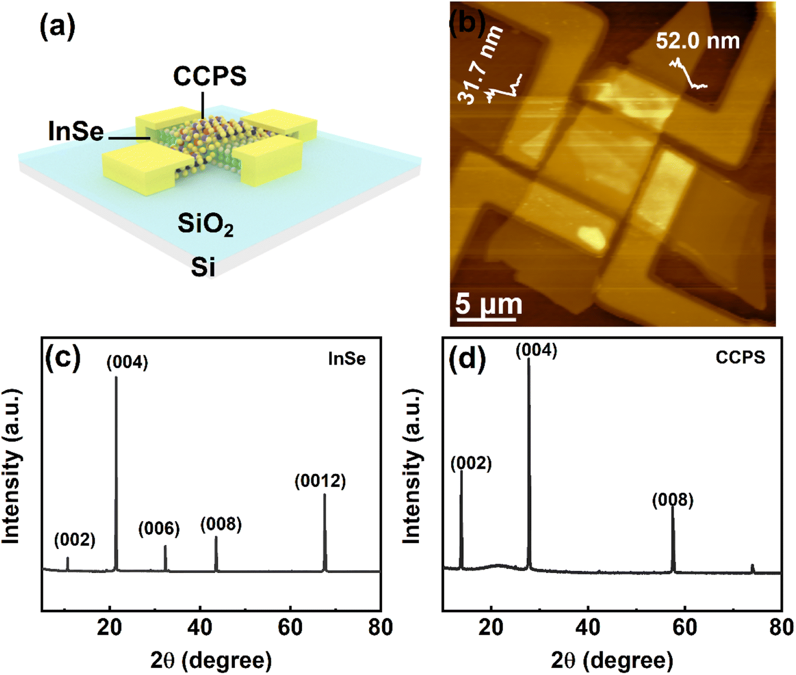 | ||
| Fig. 1 (a) Schematic illustration of InSe/CCPS device. (b) AFM topography of InSe/CCPS device. XRD spectra of (c) InSe and (d) CCPS. | ||
To study the ferroelectric properties of CCPS, we transferred CCPS flakes onto a gold-coated Si substrate and performed PFM measurements at room temperature. The in-plane (IP) and out-of-plane (OOP) phase images of CCPS were obtained by writing two square patterns with opposite end voltages. The OOP (Fig. 2(a)) and IP (Fig. 2(b)) phase images acquired after writing two square patterns with opposite tip voltages demonstrate that the external bias can control the polarization direction. Moreover, from Fig. 2(c) and (d), there is a significant 180° transition in both in-plane and out-of-plane ferroelectric polarizations. These results confirm that the CCPS shows ferroelectricity in both IP and OOP phase.
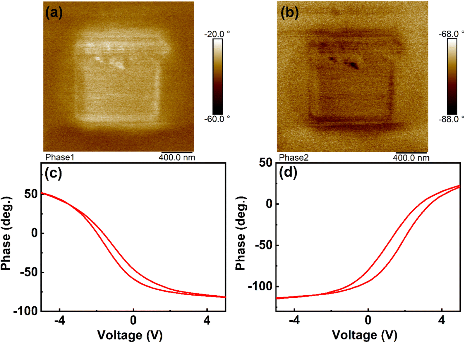 | ||
| Fig. 2 (a) Out-of-plane (OOP) and (b) in-plane (IP) phase images of CCPS. (c) OOP and (d) IP phase-voltage hysteresis of CCPS obtained by PFM. | ||
Then, we characterized the electrical performance of CCPS. The CCPS was transferred onto a SiO2/Si substrate, and two Ti/Au electrodes were fabricated to form a symmetric metal/CCPS/metal device with a channel length of 3 μm. As shown in Fig. 3(a), the Cu ions will undergo directional migration driven by the electric field in the presence of the electric field.34,35 In Fig. 3(b), we present the in-plane currents resulting from ten cycles of voltage sweeps, ranging from 0 V to +1.5 V and then −1.5 V to 0 V. During the initial phase, as the positive bias voltage increases from 0 to 1.5 V, the device transitions from a high-resistance state to a low-resistance state at a threshold voltage of 0.6 V. However, when the positive voltage is swept back, the device exhibits a noticeable hysteresis as it returns to the high-resistance state. This hysteresis loop indicates that the device displays bidirectional threshold resistive switching behavior.
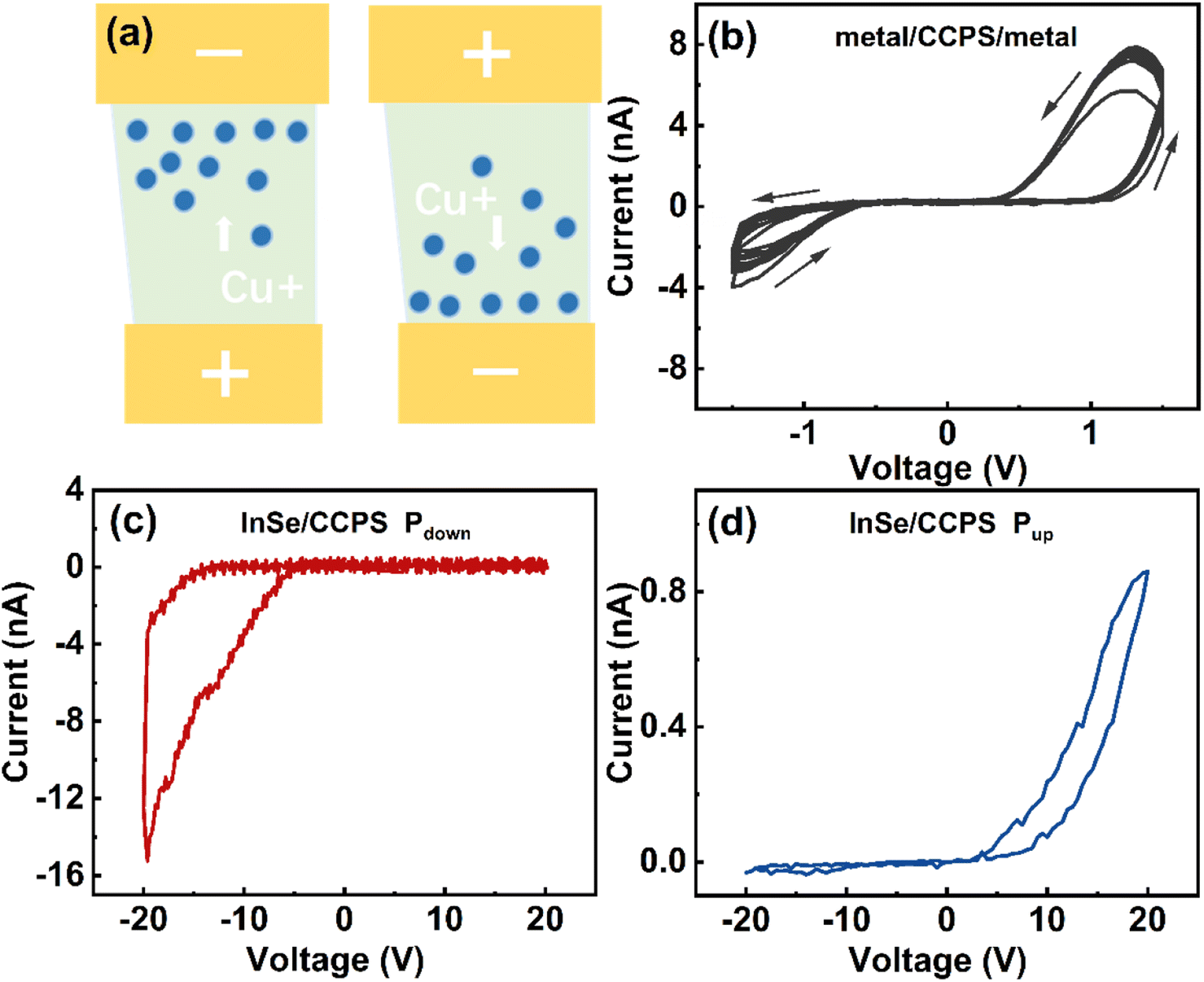 | ||
| Fig. 3 (a) Schematic illustration of Cu ion migration in CCPS. (b) I–V curves for Metal/CCPS/metal device with a ten voltage sweep from 0 V to +1.5 V and then −1.5 V to 0 V. I–V curves for InSe/CCPS bilayer device with a voltage sweep from 0 V to + 20 V and then −20 V to 0 V in (c) Pdown state and (d) Pup state. | ||
Recognizing the observed relative asymmetry between the positive and negative loops, we conducted an additional set of ten cycles, spanning from 0 V to approximately −1.5 V and then back to 0 V to −1.5 V, as depicted in Fig. S4(a) and (b) (ESI).† The resistive switching characteristics remained intact, with the currents exhibiting a relatively symmetrical response under both positive and negative biases.
A similar phenomenon is evident in the InSe/CCPS bilayer device, where the switching voltage increases to approximately 20 V due to heterojunctions and variations in channel lengths. To illustrate, after applying an IP voltage of −20 V (Pdown state) to the CCPS for 5 minutes, we conducted a voltage sweep ranging from 0 V to +20 V, followed by −20 V to 0 V, as presented in Fig. 3(c). Under positive voltage, the current consistently maintains a high-resistance state, transitioning to a low-resistance state at around −15 V and subsequently returning to a high-resistance state at −5 V before reaching 0 V. This same behavior is observed when applying a voltage of 20 V (Pup state), as depicted in Fig. 3(d). These outcomes suggest that continuous application of voltage (+20 V/−20 V) prompts a more significant migration and concentration of Cu+ ions around the cathode, resulting in an asymmetric interfacial barrier and giving rise to this rectifying behavior.
Next, we study the CCPS-controlled optoelectronic performance of InSe, as shown in Fig. 4(a). For convenience, we define the state of CCPS with 20 V applied as Pup, the state of CCPS with −20 V applied as Pdown, and the state without applied voltage as P0. Under light irradiation at a wavelength of 300 nm with a power of 50 μW cm−2 (the channel distance in InSe is 10 μm), the photocurrent is 1.2 × 10⁻⁸ A while the dark current is in the order of 9.6 × 10⁻¹⁰ A at the P0 state, demonstrating a favorable photoresponse property. Interestingly, at the Pup state, the photocurrents increase to 5.6 × 10⁻⁸ A, and the dark current decreases to 8.2 × 10⁻¹⁰ A, as shown in Fig. 4(b). In contrast, at the Pdown state, however, the photocurrent is 3.7 × 10⁻⁹ A, and the dark current is 9.3 × 10⁻¹⁰ A, as shown in Fig. 4(c). These changes in InSe photocurrents at different polarizations are attributed to the migration of Cu+ ions within the CCPS. Because the position of the CCPS is not precisely at the center of and perpendicular to the InSe channel, Cu+ ions' migration creates a built-in electric field, which impacts the InSe photocurrent at various polarizations.
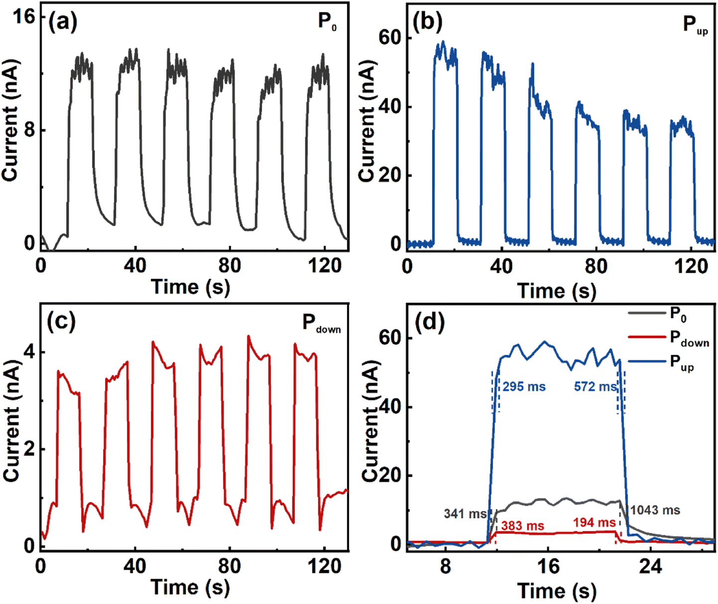 | ||
| Fig. 4 Photoresponse comparison of InSe/CCPS bilayer device under 300 nm light chopping in (a) P0, (b) Pup, and (c) Pdown state (d) Comparison of photoresponse time measurement for different polarization states (Vds of 3 V). | ||
Furthermore, we conducted measurements of the device's response time at various polarization states. In this context, we define τrise (τdecay) as the time interval required for the irradiated object to transition from 10% (90%) to 90% (10%) of the peak value. The comparative analysis of the InSe response times at different polarization states of the CCPS is depicted in Fig. 4(d).
We observe that the Pup state exhibits a faster rise time (295 ms) compared to the P0 state and a slower decay time (572 ms) compared to the Pdown state (as shown in Table 1). This behavior arises from the amplified built-in potential in the Pup state, which facilitates the rapid separation of photogenerated carriers and reduces recombination, leading to a faster rise time. The recovery time is similarly expedited, decreasing from 1043 ms to 572 ms, while the response time lengthens from 341 ms to 726 ms. This enhancement demonstrates the significant modulation effect that the CCPS exerts on the photoresponse of InSe.
| Ilight (A) | Idark (A) | R (A W−1) | D* (Jones) | τrise (ms) | τdecay (ms) | |
|---|---|---|---|---|---|---|
| Pup | 5.6 × 10⁻⁸ | 8.2 × 10⁻¹⁰ | 1839 | 1.9 × 10¹² | 295 | 572 |
| P0 | 1.2 × 10⁻⁸ | 9.6 × 10⁻¹⁰ | 368 | 1.2 × 10¹² | 341 | 1043 |
| Pdown | 3.6 × 10⁻⁹ | 9.3 × 10⁻¹⁰ | 89 | 4.6 × 10¹¹ | 383 | 194 |
To further quantitatively compare the photoresponse performance of the device in different states, we calculated parameters including responsivity (R) and detectivity (D*). The responsivity quantifies the efficiency of a device in responding to incident light and is computed using the following formula:36
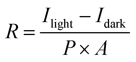
Ilight and Idark denote the current detected under illumination and in the dark, P is the intensity of the incident light, and A is the effective light area. Upon continuous application and withdrawal of a 20 V voltage, the residual polarization field of the CCPS significantly amplifies InSe's responsivity from 698 A W−1 to 1839 A W−1. Moreover, it's a substantial 20.7-fold difference in responsivity between the two polarization states. Another critical parameter is detectivity, which represents the weakest signal of light that the device can detect. Typically, it is determined using the following formula:37,38

We have measured the highest detectivity of 1.9 × 10¹² Jones at the Pup state. For better quantification, we compare the responsivity and detectivity of the different polarization states of the CCPS to InSe using the equations described above, summarized in Table 1. The PFM and the findings mentioned above suggest that the vertical upward and downward electric field components of the residual electric field of the CCPS after polarization are responsible for the formation of different performance in the Pup and Pdown states, respectively. Due to the incomplete symmetric stacking of CCPS and InSe, when the direction of the InSe photocurrent is in the same direction as the ferroelectric field of the CCPS, enhancement is exhibited, and the opposite is inhibited.
To ensure the repeatability and reliability of the observed modulation effect of CCPS, we fabricated another device (Device B) with an identical structure. The photoelectric performance is illustrated in Fig. S5 (ESI).† Notably, we observe that the photocurrents of InSe in the Pdown and Pup states were 3.8 nA and 50 nA, respectively, showcasing a significant 13.2-fold enhancement. This substantiates the reproducibility and consistency of the modulation effect.
We further study the wavelength-dependent photoresponse CuCrP2S6/InSe bilayer. In the pristine state, we tested the IV curves of InSe at different wavelengths, as shown in Fig. 5(a) (50 μW cm−2 at 300 nm, 55 μW cm−2 at 350 nm, 68 μW cm−2 at 405 nm, and 110 μW cm−2 at 520 nm) The I–V curves show an asymmetric phenomenon due to the influence of the intermediate InSe/CCPS junction region. As shown in Fig. 5(b)–(d), the CCPS still significantly affects the photocurrent of InSe after polarization under different wavelengths, and the modulation effect can be seen to be significantly different for each wavelength. To demonstrate the modulation effect of CCPS at different wavelengths, we calculate the relationship N as a function of the wavelength (N = Ilight (Pup)/Ilight (Pdown)) as shown in Fig. S6 (ESI).† It can be seen that N increases with the decrease of wavelength, with a maximum value of 14.9 at 300 nm. These findings show that photocurrent modulation via CCPS polarization is stable at broadband wavelengths, implying that the CCPS/InSe bilayer can be used as a multi-state optoelectronic memory.
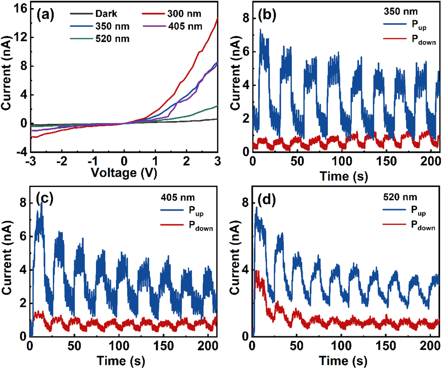 | ||
| Fig. 5 InSe/CCPS bilayer device (a) I–V curves under dark and different wavelengths. Photoresponse comparison under light chopping of (b) 350 nm, (c) 405 nm, (d) and 520 nm at Pdown and Pup states (Vds of 3 V). | ||
Conclusion
In conclusion, we have demonstrated the effective modulation of ferroelectric residual polarization in CCPS, leading to a significant impact on the optoelectronic performance of InSe. We confirm the ferroelectric properties of CCPS at room temperature in both IP and OOP orientations through PFM. The modulation results in remarkable variations in the photoresponse of InSe, with photocurrent differences of up to 14.9 times observed in different polarization states. The primary factor contributing to these variations is the asymmetry of the electric field and device structure. Our CCPS/InSe device exhibits a responsivity of 1839 A W−1 and detectivity of 1.9 × 10¹² Jones at a 300 nm wavelength. Moreover, the modulation of photoresponse remains stable across a broad spectral range spanning from 300 to 520 nm. This work shows that CuCrP2S6/InSe bilayer could be promising for polarization-enhanced photodetectors, which also suggests strong implications for the application of CuCrP2S6 in multi-state broadband optoelectronic memory and other novel non-volatile optoelectronic devices.Conflicts of interest
There are no conflict to declare.Acknowledgements
This work was supported by the National Natural Science Foundation of China (52273298 and 62250410366), the Guangdong Basic and Applied Basic Research Foundation (2022A1515010649), and the Shenzhen Science and Technology Program (JCYJ20210324095611032, JCYJ20220818102215033 and JCYJ20220818100008016). The authors acknowledge the technical support from the Photonics Centre of Shenzhen University.References
- P. V. Pham, S. C. Bodepudi, K. Shehzad, Y. Liu, Y. Xu, B. Yu and X. Duan, Chem. Rev., 2022, 122, 6514 CrossRef CAS PubMed.
- L. Cheng, X. Wang, F. Gong, T. Liu and Z. Liu, Adv. Mater., 2019, 32, 1902333 CrossRef PubMed.
- M. Dai, C. Gao, Q. Nie, Q. J. Wang, Y. F. Lin, J. Chu and W. Li, Adv. Mater. Technol., 2022, 7, 2200320 CrossRef.
- H. Ma, Y. Xing, J. Han, B. Cui, T. Lei, H. Tu, B. Guan, Z. Zeng, B. Zhang and W. Lv, Adv. Opt. Mater., 2021, 10, 2101772 CrossRef.
- W. Ahmad, J. Liu, J. Jiang, Q. Hao, D. Wu, Y. Ke, H. Gan, V. Laxmi, Z. Ouyang, F. Ouyang, Z. Wang, F. Liu, D. Qi and W. Zhang, Adv. Funct. Mater., 2021, 31, 2101772 CrossRef.
- J. Li, Y. Chen, Y. Li, H. Zhu and L. Li, Appl. Phys. Express, 2023, 16, 1 Search PubMed.
- W. G. Luo, Y. F. Cao, P. G. Hu, K. M. Cai, Q. Feng, F. G. Yan, T. F. Yan, X. H. Zhang and K. Y. Wang, Adv. Opt. Mater., 2015, 3, 1418 CrossRef CAS.
- X. Yang, X. Liu, L. Qu, F. Gao, Y. Xu, M. Cui, H. Yu, Y. Wang, P. Hu and W. Feng, ACS Nano, 2022, 16, 8440 CrossRef CAS PubMed.
- H. W. Yang, H. F. Hsieh, R. S. Chen, C. H. Ho, K. Y. Lee and L. C. Chao, ACS Appl. Mater. Interfaces, 2018, 10, 5740 CrossRef CAS PubMed.
- A. Ren, L. Yuan, H. Xu, J. Wu and Z. Wang, J. Mater. Chem. C, 2019, 7, 14441 RSC.
- J. Jiang, Y. Guo, X. Weng, F. Long, Y. Xin, Y. Lu, Z. Ye, S. Ruan and Y.-J. Zeng, J. Mater. Chem. C, 2021, 9, 4978 RSC.
- X. Zhou, X. Hu, S. Zhou, H. Song, Q. Zhang, L. Pi, L. Li, H. Li, J. Lu and T. Zhai, Adv. Mater., 2018, 30, 1703286 CrossRef PubMed.
- Y. Yan, G. Abbas, F. Li, Y. Li, B. Zheng, H. Wang and F. Liu, Adv. Mater. Interfaces, 2022, 9, 2102068 CrossRef CAS.
- N. Hu, D. Jiang, G. Zhang, Z. Guo, W. Zhang, X. Yang, S. Gao, T. Zheng, Q. Liang and J. Hou, Mater. Res. Bull., 2018, 103, 294 CrossRef CAS.
- H. W. Xie, C. X. Kang, M. A. Iqbal, X. L. Weng, K. W. Wu, W. Tang, L. Qi and Y. J. Zeng, Nanomaterials, 2022, 12, 3358 CrossRef CAS PubMed.
- H. Zhu, J. Li, Q. Chen, W. Tang, X. Fan, F. Li and L. Li, ACS Nano, 2023, 17, 1239 CrossRef CAS PubMed.
- M. A. Iqbal, H. Xie, L. Qi, W. C. Jiang and Y. J. Zeng, Small, 2023, 19, 2205347 CrossRef CAS PubMed.
- Y. Guo, Z. Xu, A. G. Curto, Y.-J. Zeng and D. Van Thourhout, Prog. Mater. Sci., 2023, 138, 101158 CrossRef CAS.
- C. Zhu, Y. Wang, F. Wang, J. Yang, X. Zhan, L. Fang, Z. Wang and J. He, Appl. Phys. Lett., 2022, 120, 083101 CrossRef CAS.
- S. Wan, Y. Li, W. Li, X. Mao, C. Wang, C. Chen, J. Dong, A. Nie, J. Xiang, Z. Liu, W. Zhu and H. Zeng, Adv. Funct. Mater., 2019, 29, 180806 Search PubMed.
- M. Kumar and H. Seo, Adv. Mater., 2022, 34, 10 Search PubMed.
- J. Liu, K. W. Yi, Z. P. Wang, Z. J. Zhang, Y. C. Qi, P. Chen, Q. D. Shen and B. J. Chu, Sci. China Mater., 2021, 64, 1197 CrossRef CAS.
- J. Yue and Z. Li, J. Synth Cryst., 2018, 47, 594 CAS.
- C. Jia, S. X. Wu, J. Fan, C. Luo, M. Fan, M. Li, L. He, Y. Yang and H. Zhang, ACS Nano, 2023, 17, 6534 CrossRef CAS.
- Z. Zhao, S. Rakheja and W. Zhu, Nano Lett., 2021, 21, 9318 CrossRef CAS.
- X. L. Wang, Z. X. Shang, C. Zhang, J. Q. Kang, T. Liu, X. Y. Wang, S. L. Chen, H. L. Liu, W. Tang, Y. J. Zeng, J. F. Guo, Z. H. Cheng, L. Liu, D. Pan, S. C. Tong, B. Wu, Y. Y. Xie, G. C. Wang, J. X. Deng, T. R. Zhai, H. X. Deng, J. W. Hong and J. H. Zhao, Nat. Commun., 2023, 14, 840 CrossRef CAS.
- W. Tang, D. Zhao, X. Weng, K. Wu, Z. Yang, C. Kang, Y. Sun, W.-C. Jiang, H. Liang, C. Wang and Y.-J. Zeng, Appl. Phys. Rev., 2023, 10, 031404 CAS.
- Y. F. Lai, Z. G. Song, Y. Wan, M. Z. Xue, C. S. Wang, Y. Ye, L. Dai, Z. D. Zhang, W. Y. Yang, H. L. Du and J. B. Yang, Nanoscale, 2019, 11, 5163 RSC.
- K. Cho, S. Lee, R. Kalaivanan, R. Sankar, K. Y. Choi and S. Park, Adv. Funct. Mater., 2022, 32, 2204214 CrossRef CAS.
- Y. D. Ma, Y. Dai, L. Yu, C. W. Niu and B. B. Huang, New J. Phys., 2013, 15, 11 Search PubMed.
- D. K. Sang, H. D. Wang, M. Qiu, R. Cao, Z. N. Guo, J. L. Zhao, Y. Li, Q. L. Xiao, D. Y. Fan and H. Zhang, Nanomaterials, 2019, 9, 13 Search PubMed.
- H. W. Hu, Y. L. Sun, M. S. Chai, D. Xie, J. Ma and H. W. Zhu, Appl. Phys. Lett., 2019, 114, 4 Search PubMed.
- M. A. Susner, R. Rao, A. T. Pelton, M. V. McLeod and B. Maruyama, Phys. Rev. Mater., 2020, 4, 10 Search PubMed.
- C. B. Park, A. Shahee, K. T. Kim, D. R. Patil, S. A. Guda, N. Ter-Oganessian and K. H. Kim, Adv. Electrode Mater., 2022, 8, 2101072 CrossRef CAS.
- X. Jiang, X. Wang, X. Wang, X. Zhang, R. Niu, J. Deng, S. Xu, Y. Lun, Y. Liu, T. Xia, J. Lu and J. Hong, Nat. Commun., 2022, 13, 574 CrossRef CAS PubMed.
- L. L. Shi, K. Q. Chen, A. P. Zhai, G. H. Li, M. M. Fan, Y. Y. Hao, F. R. Zhu, H. Zhang and Y. X. Cui, Laser Photonics Rev., 2021, 15, 31 Search PubMed.
- F. Wang, Z. X. Wang, L. Yin, R. Q. Cheng, J. J. Wang, Y. Wen, T. A. Shifa, F. M. Wang, Y. Zhang, X. Y. Zhan and J. He, Chem. Soc. Rev., 2018, 47, 6296 RSC.
- H. Qiao, Z. Y. Huang, X. H. Ren, S. H. Liu, Y. P. Zhang, X. Qi and H. Zhang, Adv. Opt. Mater., 2020, 8, 20 Search PubMed.
Footnote |
| † Electronic supplementary information (ESI) available. See DOI: https://doi.org/10.1039/d3ra05888c |
| This journal is © The Royal Society of Chemistry 2023 |