
 Open Access Article
 This Open Access Article is licensed under a
 Creative Commons Attribution 3.0 Unported Licence
Visible light activated SnO2:Dy thin films for the photocatalytic degradation of methylene blue
M. Mezyen*a,
G. El Fidhaab,
N. Bitria,
F. Harrathiab,
I. Lyc and
E. Llobet *d
*d
aUniversité de Tunis El Manar, Ecole Nationale d'Ingénieurs de Tunis, Laboratoire de Photovoltaïque et Matériaux Semi-conducteurs, 1002 Tunis, Tunisia. E-mail: marwenmezyen@gmail.com
bEcole Nationale Supérieure d'ingénieurs de Tunis (ENSIT), Avenue Taha Hussein Montfleury, Tunis 1008, Tunisia
cCentre de Recherche Paul Pascal (CRPP) – UMR 5031, 115 Avenue Albert Schweitzer, 33600 Pessac, France
dUniversitat Rovira i Virgili, MINOS, ETSE, Avda. Països Catalans, Tarragona, 2643007, Spain. E-mail: eduard.llobet@urv.cat
First published on 24th October 2023
Abstract
This paper explores the impact of dysprosium (Dy) doping on structural, optical, and photocatalytic properties of tin oxide (SnO2) thin films fabricated via spray pyrolysis. Dysprosium doping levels ranged from 0 to 7 at%, and films were grown on glass substrates at 350 °C. X-ray diffraction (XRD) analysis revealed an increase in crystallite size with Dy doping, signifying improved crystalline quality. Simultaneously, dislocation density and strain decreased, indicating enhanced film quality. Texture coefficient (Tchkl) results showed a predominant crystal orientation along the (110) plane due to Dy doping. Optical band gap energy (Eg) decreased with Dy doping up to 5%. Urbach energy increased with Dy doping, suggesting atomic structural flaws and defects. Scanning electron microscopy (SEM) analysis revealed the presence of numerous micro-aggregates on the film's surface. Notably, the density of these micro-aggregates increased proportionally with higher Dy doping levels, particularly emphasizing the pronounced effect observed in SnO2:Dy 5% thin films. These findings underscore the potential of Dy-doped SnO2 thin films for advanced photocatalytic applications, with SnO2:Dy 5% exhibiting favorable properties and demonstrating a 90.99% degradation efficiency in three hours under solar irradiation.
1 Introduction
Dyes encompass a category of colored aromatic organic compounds known for their light-absorbing properties, which contribute to their ability to introduce color into the visible spectrum.1,2 Various industries, including textiles, food, rubber, printing, cosmetics, medicine, plastics, concrete, and the paper industry, employ a wide range of dyes for various purposes.3 It is estimated that there are over 100![[thin space (1/6-em)]](https://www.rsc.org/images/entities/char_2009.gif) 000 commercially utilized dyes globally, with an annual production volume ranging from approximately 7 × 10⁸ to 1 × 10⁹ kilograms.4 Unfortunately, these industries produce substantial amounts of wastewater that often contains carcinogenic and toxic dyes, thereby contaminating water sources and rendering them unsuitable for human consumption.5 Among these sectors, the textile industry stands out as the largest consumer of dyes, with textile dyes being particularly complex compounds featuring diverse structural groups.10 Notably, Methylene Blue (MB) is one of the most heavily used substances in the dye industry, finding common application in the coloring of silk, wool, cotton, and paper.6–8 MB is classified as an aromatic heterocyclic basic dye.9 It is widely recognized as a cationic primary thiazine dye, characterized by its molecular formula C16H18N3ClS and an absorption maximum λmax at 663 nm. Remarkably, MB exhibits exceptional water solubility, forming a stable solution with water even at room temperature.10–13 Therefore, many efforts have been devoted to remove MB dye from waste water including adsorption,14–16 chemical precipitation and some biological means but for their limitations. Photocatalysis, an advanced oxidation process, is highly efficient, cost effective; eco-friendly and stable photocatalysts have found their routes through semiconductors in nano forms. Transparent Conductive Oxides (TCOs) such as TiO2, SnO2, ZnO, Fe2O3 and CdO, have been proven to be suitable photocatalysts for the removal of organic water pollutants.17–19 Among all these and other photocatalysts, tin oxide (SnO2) has gained more attention due to its numerous properties including high charge carrier mobility, a wide band gap, excellent transparency, ease of tunability, as well as remarkable thermal and chemical stability.20 Enhancing the photocatalytic performance of SnO2 has been a subject of study, with significant improvements achieved through doping with transition metals or their oxides such as Cu,21 Ni, Sb,22 Co, Fe, and Mg.23 This modification has been shown in the literature to influence shifts in optical absorption, elevate surface defect levels, increase the generation of surface oxygen vacancies, and impede charge carrier recombination.24–27 Recently, rare earth (RE) metals have been explored as additives due to their interactive electron configuration, excellent catalytic properties and fast oxygen ion mobility, which tend to enhance the speed of degradation by making up for the shortcomings in the structure of the thin films. These interesting materials involve a wide range of elements including Ce,28 Y,29 Tm,30 Tb,31 Nd32 and Pr.33 Numerous studies have investigated the impact of doping with rare earth elements on the structural and photocatalytic properties of thin films. For instance, Loyola et al.34 explored the synergistic effect of terbium (Tb) doping on SnO2 thin films, prepared through nebulized spray pyrolysis and demonstrated an impressive 85% degradation efficiency for 10−5 M methylene blue (MB) dye aqueous solution. Similarly, Ayadi et al.35 examined the influence of cerium (Ce) doping on SnO2 thin films, also prepared using spray pyrolysis, and achieved a noteworthy 19.10% degradation of MB dye under UV irradiation. Their results highlighted that the photocatalytic performance was significantly enhanced by the presence of a mixture of tetragonal and cubic phases, particularly with a 2 wt% Ce doping. These two exemplary studies illustrate the profound impact of rare earth element doping on thin films' photocatalytic capabilities and provide valuable insights into the optimization of such materials for efficient dye degradation. Dysprosium (Dy), being among the most abundant rare earth elements, exhibits high surface reactivity, rapidly oxidizing in the presence of air and readily reacting with water to release dihydrogen. Introducing Dy-doping into TCOs has been observed to enhance visible light absorption and suppress the recombination of photo-generated electrons and holes, thus making it a favorable choice for photocatalytic applications.36 In this study, Dy-doped SnO2 thin films were prepared by means of spray pyrolysis. In contrast to many other film deposition processes, this technique is a fairly straightforward and comparatively inexpensive processing approach (low-cost equipment used). It is an incredibly simple method for creating films of any composition. Spray pyrolysis does not require premium chemicals or substrates, and can be used to deposit thick films, porous films, and to create powder. This adaptable method makes it simple to produce multi-layered films. To the best of our knowledge, spray pyrolysis has never been used to develop Dy-doped SnO2 thin films for photocatalysis applications. The main goal of this study was to determine how dysprosium dopant affects the structural, morphological, optical, chemical and electrical properties of SnO2 thin films, specifically by studying how the use of rare-earth dysprosium as a dopant helps improve the photocatalytic performance of thin films made of SnO2 by focusing on the effects of time, dye concentration, and sample composition on the degradation efficiency of MB.
000 commercially utilized dyes globally, with an annual production volume ranging from approximately 7 × 10⁸ to 1 × 10⁹ kilograms.4 Unfortunately, these industries produce substantial amounts of wastewater that often contains carcinogenic and toxic dyes, thereby contaminating water sources and rendering them unsuitable for human consumption.5 Among these sectors, the textile industry stands out as the largest consumer of dyes, with textile dyes being particularly complex compounds featuring diverse structural groups.10 Notably, Methylene Blue (MB) is one of the most heavily used substances in the dye industry, finding common application in the coloring of silk, wool, cotton, and paper.6–8 MB is classified as an aromatic heterocyclic basic dye.9 It is widely recognized as a cationic primary thiazine dye, characterized by its molecular formula C16H18N3ClS and an absorption maximum λmax at 663 nm. Remarkably, MB exhibits exceptional water solubility, forming a stable solution with water even at room temperature.10–13 Therefore, many efforts have been devoted to remove MB dye from waste water including adsorption,14–16 chemical precipitation and some biological means but for their limitations. Photocatalysis, an advanced oxidation process, is highly efficient, cost effective; eco-friendly and stable photocatalysts have found their routes through semiconductors in nano forms. Transparent Conductive Oxides (TCOs) such as TiO2, SnO2, ZnO, Fe2O3 and CdO, have been proven to be suitable photocatalysts for the removal of organic water pollutants.17–19 Among all these and other photocatalysts, tin oxide (SnO2) has gained more attention due to its numerous properties including high charge carrier mobility, a wide band gap, excellent transparency, ease of tunability, as well as remarkable thermal and chemical stability.20 Enhancing the photocatalytic performance of SnO2 has been a subject of study, with significant improvements achieved through doping with transition metals or their oxides such as Cu,21 Ni, Sb,22 Co, Fe, and Mg.23 This modification has been shown in the literature to influence shifts in optical absorption, elevate surface defect levels, increase the generation of surface oxygen vacancies, and impede charge carrier recombination.24–27 Recently, rare earth (RE) metals have been explored as additives due to their interactive electron configuration, excellent catalytic properties and fast oxygen ion mobility, which tend to enhance the speed of degradation by making up for the shortcomings in the structure of the thin films. These interesting materials involve a wide range of elements including Ce,28 Y,29 Tm,30 Tb,31 Nd32 and Pr.33 Numerous studies have investigated the impact of doping with rare earth elements on the structural and photocatalytic properties of thin films. For instance, Loyola et al.34 explored the synergistic effect of terbium (Tb) doping on SnO2 thin films, prepared through nebulized spray pyrolysis and demonstrated an impressive 85% degradation efficiency for 10−5 M methylene blue (MB) dye aqueous solution. Similarly, Ayadi et al.35 examined the influence of cerium (Ce) doping on SnO2 thin films, also prepared using spray pyrolysis, and achieved a noteworthy 19.10% degradation of MB dye under UV irradiation. Their results highlighted that the photocatalytic performance was significantly enhanced by the presence of a mixture of tetragonal and cubic phases, particularly with a 2 wt% Ce doping. These two exemplary studies illustrate the profound impact of rare earth element doping on thin films' photocatalytic capabilities and provide valuable insights into the optimization of such materials for efficient dye degradation. Dysprosium (Dy), being among the most abundant rare earth elements, exhibits high surface reactivity, rapidly oxidizing in the presence of air and readily reacting with water to release dihydrogen. Introducing Dy-doping into TCOs has been observed to enhance visible light absorption and suppress the recombination of photo-generated electrons and holes, thus making it a favorable choice for photocatalytic applications.36 In this study, Dy-doped SnO2 thin films were prepared by means of spray pyrolysis. In contrast to many other film deposition processes, this technique is a fairly straightforward and comparatively inexpensive processing approach (low-cost equipment used). It is an incredibly simple method for creating films of any composition. Spray pyrolysis does not require premium chemicals or substrates, and can be used to deposit thick films, porous films, and to create powder. This adaptable method makes it simple to produce multi-layered films. To the best of our knowledge, spray pyrolysis has never been used to develop Dy-doped SnO2 thin films for photocatalysis applications. The main goal of this study was to determine how dysprosium dopant affects the structural, morphological, optical, chemical and electrical properties of SnO2 thin films, specifically by studying how the use of rare-earth dysprosium as a dopant helps improve the photocatalytic performance of thin films made of SnO2 by focusing on the effects of time, dye concentration, and sample composition on the degradation efficiency of MB.
2 Materials and methods
2.1 Preparation of the thin films
Several separate steps were performed prior to the spraying stage. The glass substrate was treated following a specific cleaning protocol to eliminate impurities using detergent, ionized water, acetone and 1/4 HNO3 + 3/4 HCl. The substrate was then dried in an oven at a temperature of 120 °C. The dysprosium (Dy) doped and undoped SnO2 thin layers were prepared using a chemical spray pyrolysis technique on a glass substrate heated to a fixed temperature of 350 °C as presented in Fig. 1. Meanwhile, the SnO2 solution was prepared by dissolving 0.05 M of tin(II) chloride SnCl2 (99.9%, Sigma-Aldrich) in 40 mL of distilled water. For the doped thin films, the dysprosium DyCl3 (DyCl3·2H2O, Sigma-Aldrich) was mixed with the precursor before being dissolved in concentration ratios of 1, 3, 5 and 7 at%. Since SnO2 is insoluble in water, it must undergo continuous magnetic stirring prior to and throughout the entire deposition period with heating to just 30 °C, and with the addition of a few drops of HCl. Tin oxide thin film deposition on a glass substrate is anticipated to occur after the chemical reaction as:| SnCl2+ H2O → SnO +2HCl | (1) |
| SnO + 1/2O2 → SnO2 | (2) |
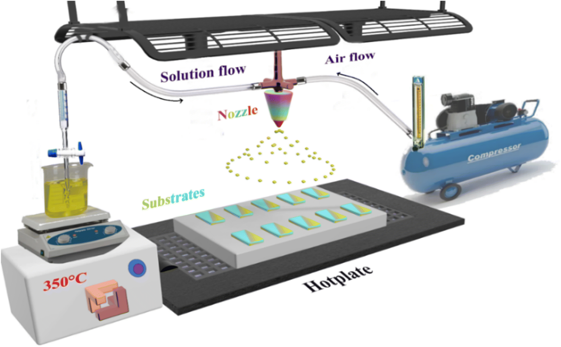 | ||
| Fig. 1 Spray pyrolysis method. | ||
The solution was sprayed for 10 min at a solution flow of 4 mL min−1. All the parameters were controlled, including air compression carrying gas at a fixed flow of 10 mL min−1 and substrate temperatures maintained at 350 °C through a thermocouple connected to the hotplate on which the substrates were placed. The space between the nozzle and the substrates was estimated to 20 cm.
All these conditions were designed to promote the formation of the thin layer by maintaining contact between droplets of the solution and the substrates.
2.2 Characterization of the thin films
The thin films obtained in the spraying process were then characterized. Their structural properties were determined using X-ray diffraction (XRD) with a Philips X'pert diffractometer with Cu Kα radiation (λ = 1.5406 Å) granting a diffraction angle (2θ) ranging between 20° and 70°. Optical properties like transmittance and reflectance were obtained using a spectrophotometer (Shimadzu-UV 1800) providing a scan range of between 300 and 1800 nm.While the measurement of electrical properties such as resistance and resistivity were taken by means of the four-point technique using a Jandel four-point probe head, the factor shape of which is widely known, coupled to an HP 3458A multimeter (Agilent). Field emission scanning electron microscopy was used to examine the surface morphology of the synthesized thin films (FE-SEM JEOL JSM-7800 F).
2.3 Photocatalytic tests
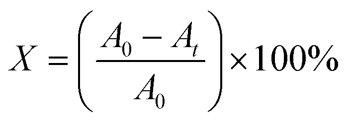
The photocatalytic efficiency of pure and Dy-doped (1, 3, 5, and 7% at.) SnO2 layers was tested using methylene blue dye (MB). Degradation occurred under solar irradiation (temperature: 35 °C, latitude: 11.24°, northern Tunisia). The photodegradation of MB was conducted using an estimated power level in the range of 180 to 230 W m−2. Each of the 5 thin layers were placed in a 40 mL glass container and totally immersed in methylene blue aqueous solution at different concentrations of 2, 3 and 4 mg L−1. Next, pure and Dy-doped SnO2 layers (1%, 3%, 5%, and 7% at.) were magnetically swirled for 30 minutes, and then left in the dark. This process ensured the balanced adsorption and desorption of the photocatalyst and the dye. Lastly, the samples and solution were exposed to solar irradiation for three hours, with a 3 mL sample taken each hour.The residual content was determined by a degradation rate X defined as follows:37
 | (3) |
3 Results and discussion
3.1 Structural properties: XRD analysis
The XRD patterns of undoped and Dy-doped SnO2 [1, 3, 5 and 7% at.] thin films are shown in Fig. 2a. All of the XRD patterns are indexed in agreement with standard JCPDS 00-041-1445. The peaks are well identified at the positions 2θ = 26.6, 34.4, 38 and 51.5° corresponding to the (hkl) planes (110), (101), (200), and (210) respectively, which confirms the tetragonal rutile structure of the SnO2 and SnO2:Dy thin films with a preferential direction of (110). In Fig. 2b, the 2θ angle corresponding to the peak (110) is depicted. A slight shift towards higher angles is noticeable as the dopant concentration increases. This shift can be attributed to the integration of Dy ions into the SnO2 crystal structure.38 All the peaks detected in the spectra are almost identical, except for thin layers based on SnO2:Dy 7%, where the two peaks at positions 2θ = (101) and (200) disappear. This may be caused by the excess presence of the Dy3+ ion triggering the incipient destruction of the lattice structures of the SnO2. According to Table 1, there is not a big difference between the lattice parameters, which increase slightly with increasing the rate of Dy-dopant. It is worth noting that the absence of any additional phases of Dy peaks like Dy2O3 in any of the patterns indicates the successful incorporation of the dopant particles in the matrix of the SnO2.39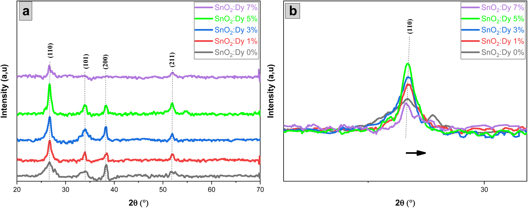 | ||
| Fig. 2 (a) XRD pattern of sprayed undoped and Dy-doped [1, 3, 5 and 7% at.] SnO2 thin films, (b) shifting of the main diffraction angle with increasing doping concentrations. | ||
| Samples | (hkl) | 2𝜃(°) | dhkl (Å) | a (Å) | c (Å) | D (nm) | δ (10−3) (nm−2) | ε (10−3) (rad) | V (nm3) | N | Tc110 |
|---|---|---|---|---|---|---|---|---|---|---|---|
| SnO2:Dy 0% | (110) | 26.69 | 3.34 | 4.71 | 3.17 | 6.90 | 21.00 | 5.47 | 70.32 | 0.05 | 1.07 |
| SnO2:Dy 1% | (110) | 26.75 | 3.34 | 4.73 | 3.18 | 12.59 | 6.31 | 2.66 | 71.15 | 0.09 | 1.07 |
| SnO2:Dy 3% | (110) | 26.84 | 3.33 | 4.72 | 3.17 | 13.00 | 5.92 | 2.75 | 70.62 | 0.10 | 1.08 |
| SnO2:Dy 5% | (110) | 26.64 | 3.35 | 4.74 | 3.19 | 14.86 | 4.53 | 2.44 | 71.67 | 0.11 | 1.19 |
| SnO2:Dy 7% | (110) | 26.60 | 3.35 | 4.75 | 3.19 | 7.00 | 20.00 | 4.93 | 71.97 | 0.05 | 1.20 |
The effect of Dy doping is very clear. When the doping rate increase, the intensity of the peaks also increase, with the maximum effect detected in the SnO2:Dy 5% layers. In order to better observe the effect of Dy doping on the thin film structures, several structural parameters should be described such as inter-lattice distances dhkl, lattice parameters (hkl), crystallite sizes (D) as well as other parameters, which are summarized in Table 1.
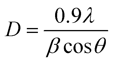
The crystallite size (D) of pure and Dy-doped SnO2 thin films are evaluated using the Debye Scherrer equation:40
 | (4) |
It has been noted that D increased with the increase in doping rate up to the highest value of 14.86 nm recorded for the SnO2 thin films doped at 5% Dy, suggesting an enhancement in crystalline quality, as shown in Fig. 2.
The dislocation density (δ) which provide information about the film's quality and any flaws in the material,41 is determined using the eqn (5):43
 | (5) |
A decrease with the increase of the dopant to reach minimum values of 4.53 × 10⁻³ nm−2 for the 5% Dy dopant was observed.42
The strain is determined by the eqn (6) below43 is tabulated in Table 1:
 | (6) |
The strain was decreased with the increase of Dy to attend 2.44 × 10⁻³ rad for the 5% thin film, then an increase was subsequently recorded for layers doped to 7%.44
The unit cell volume was determined using the eqn (7):
| V = a2 × c | (7) |
The rise in SnO2 crystallite size can be greatly suppressed by doping with Dy, and grain refinement can be accelerated. In addition, the SnO2:Dy 5% thin layers yielded the maximum number of unit cells.
The number of unit cells is calculated using the eqn (8):45
 | (8) |
The texture coefficient (Tchkl) which measures the relative degree of preferential orientation of a plane (hkl) is determined according to the following formula:46,47
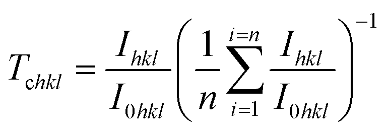 | (9) |
When Tc = 1, the crystallites are randomly oriented while the abundance of crystallites in a given plane is indicated by Tc > 1. If 0 < Tc < 1, this can denotes the absence of crystallite orientation in this direction.
The texture coefficient for the non-doped and Dy-doped SnO2 layers is greater than 1, indicating the predominant tendency of the crystals to be oriented along the (110) plane. The increase in the texture coefficient indicates that the Sn particles have been replaced by the Dy3+ ions.48
3.2 Optical properties
Fig. 3 shows the variation of the transmittance and reflection spectra in the 300–1800 nm wavelength range for the pure and Dy-doped SnO2 thin films. As the figure shows, all of the thin films exhibited high transmittance levels, with transmittance reaching up to 80% in the NIR, in good agreement with what could be expected from a (TCO). Transparency decreased slightly as Dy doping increased. The high transparency of these samples would enable their use as an optical window in solar cell applications.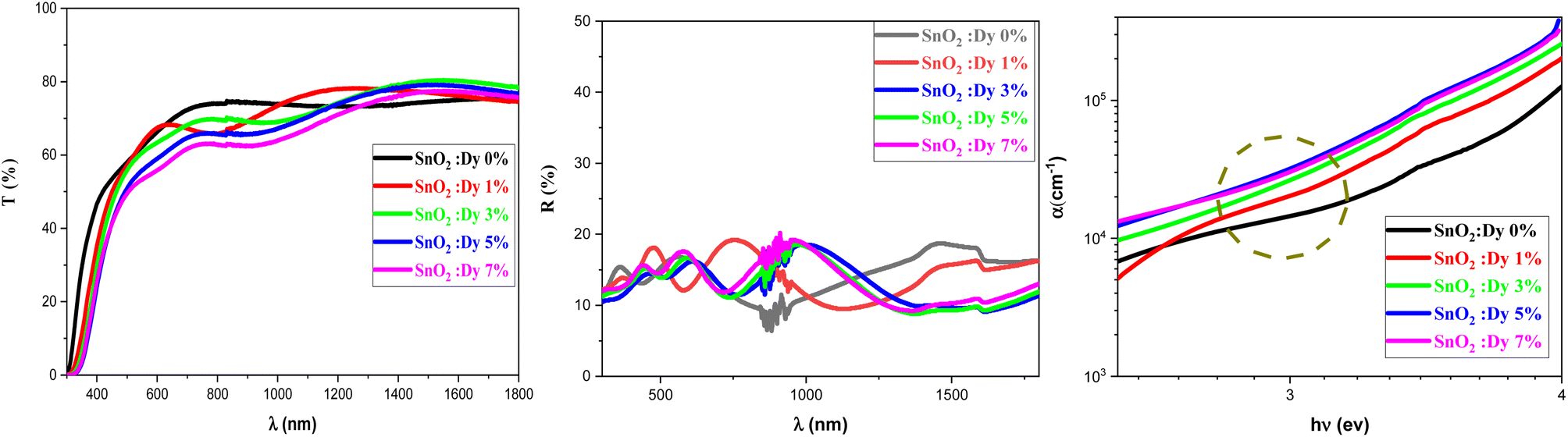 | ||
| Fig. 3 Transmission, reflection and absorption coefficient spectra of SnO2:Dy [0, 1, 3, 5 and 7% at.] thin films. | ||
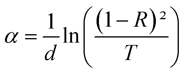
It is important to note the presence of several interference fringes (oscillations with minima and maxima) in the recorded reflection spectra. This is clearly caused by a multiple reflection phenomenon occurring between the free surface and the surface in contact with the substrate. The thickness of the SnO2:Dy thin films can be estimated using a common technique, from the locations of the interference reflectance minima and maxima.49 The values of the thickness of the SnO2:Dy films are illustrated in Table 2, which show that Dy doping increased the thickness of the thin layers. The thickness of thin films made by spray pyrolysis greatly depends on factors such as the concentration of the precursor, the substrate treatment and controlling the spray duration. Doping can generate molecular interactions, which leads to condensed films.
| Sample | SnO2:Dy 0% | SnO2:Dy 1% | SnO2:Dy 3% | SnO2:Dy 5% | SnO2:Dy 7% |
|---|---|---|---|---|---|
| Thickness (nm) | 239 ± 10 | 320 ± 10 | 373 ± 10 | 380 ± 10 | 381 ± 10 |
| Eg (eV) | 3.91 | 3.72 | 3.63 | 3.56 | 3.58 |
| Eu (meV) | 232 | 458 | 460 | 490 | 526 |
The reflection rates are between 15 and 20%. In addition, the optical absorption edge of Dy-doped SnO2 films is red-shifted compared to pure samples, moving forward to the visible light region. This red shift may be due to the formation of shallow electronic levels within the band gap arising from dopant atoms present in the lattice.50
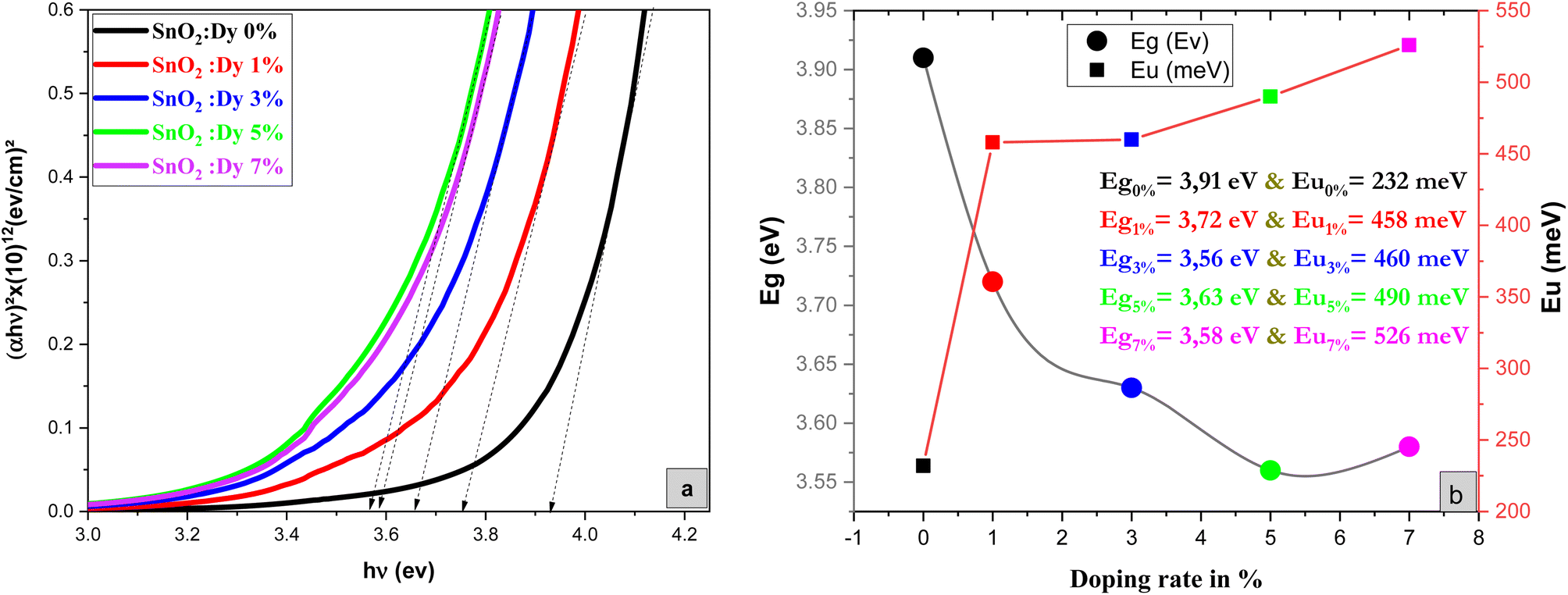
By plotting (αhν)2 as a function of (hν) and based on the Tauc model51 indicated in eqn (10), the gap energy was easily estimated the by extrapolating the linear portion of the plots of (αhν)2 versus hν to hν = 0 and based on the Tauc model interpreted by the following equations:
| (αhν) = B(hν − Eg)n | (10) |
 | (11) |
Eg is the optical band gap energy presenting the minimum required energy to excite an electron from the valence band to the conduction band and n is a fraction whose values depend on the nature of the transition (1/2, 2, 3/2 and 3). In our case, n takes 1/2 as a value, which is consistent with direct-allowed transitions.52,53
As demonstrated in Fig. 4, the presence of a linear portion in the band gap versus doping level plot confirms that our material maintains its character as a direct gap semiconductor. The reduction in band gap energy from 3.91 eV to 3.56 eV, observed as the percentage of Dy doping increases up to 5%, can be primarily attributed to the incorporation of Dy ions into the SnO2 crystal structure. Dy doping induces lattice distortion and disorder, which, in turn, affects the electronic structure of the material. This distortion results in a reduction of the band gap, as Dy contributes additional energy levels within the band structure. It's important to note that this reduction in the band gap is a characteristic effect of doping and is a well-documented phenomenon in the literature. Beyond the 5% doping level, a slight increase in the band gap is observed. This behavior may be related to the saturation effect of doping, where excessive dopant concentrations can lead to the formation of new phases, lattice defects, or other structural changes, all of which can influence the band gap. These effects are in accordance XRD results.
 | ||
| Fig. 4 (a) Plot of (αhν)2 versus (hν) of undoped and Dy-doped SnO2 thin films, (b) variation of Eg and Eu versus variation of doping rates of Dy. | ||
Meanwhile the increase in the gap in the 7% doped film can be explained by the Burstein-Moss effect, which is an increase in the absorption edge generated when the electrons require more energy to go from the valence band to the conduction band when the Fermi level, located within the conduction in the case of n type semiconductor, shifts further in the conduction band, resulting in the widening of the band gap of the film.54 Palanichamy et al. reported similar band gap variations for (Gd3+)-doped SnO2 thin films prepared with a simplified spray pyrolysis technique using a nebulizer.55 We should note that the optical band gap of the film is also known to be effectively changed by defects like impurities, interstitials, oxygen vacancies, and substitutional defects.
This displacement of the energy gap might be in part attributed to the implementation of defects and disorder in the SnO2 lattice due to the incorporation of dopants, which has the effect of forming localized states and deep levels in the band gap, which allows the general structure of it to change.56 The spectral lines depicted in Fig. 3c show the values of the absorption coefficient of the synthesized thin films as a function of the photon energy. Dysprosium doping caused an increase in optical absorption across all layers, which is consistent with the findings of Gnanasekar et al.,57 who showed that such doping could give rise to changes in the optical properties of CuO, allowing them to be used for applications that involve radiations and chemical reactions. The values of the absorption coefficients were very high with an average value of 105 cm−1 for all thin films, giving our thin films the absorbent character they need for good photocatalytic performance.
In semiconducting materials, structural disorder produces localized states, also known as band tails, around the margins of prohibited bands. The Urbach Energy, also known as the Urbach tail, is the exponentially increasing absorption edge located close to the fundamental band gap.58 The Urbach Energy can be used to determine the lattice defect concentration because it characterizes the breadth of the localized states in the principal optical band gap. The following relation is used to assess the Urbach tail:
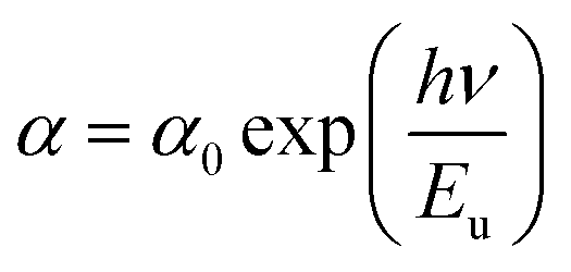 | (12) |
Fig. 4b shows that Eu increased as Dy doping increased, going from 232 to 526 meV, which demonstrates that atomic structural flaws occurred. The increase in the Urbach Energy values with the increase in Dy doping concentration suggests that the band gap structure of the thin films doped with Dy had more defects than before. Actually, the optical data might lead one to believe that Dy atoms were successfully incorporated into the SnO2 lattice. The shrinkage of the optical band gap also explains the rise in the Urbach Energy,59 as shown in Fig. 4b.
3.3 Morphological characterization
SEM is used to analyze the surface morphology of pure and Dy-doped SnO2 thin films. The morphological modification in the SnO2 thin film samples at various doping rates (0, 1, 3, 5 and 7% at.) are shown in Fig. 5. These figures suggest that for pure SnO2, the grains do not seem to be tightly packed, leaving noticeable voids in the sample. Numerous microscopic grains multiplied and collected to create a grainy surface with the appearance of gaps and fissures as the rate of Dy increased at 1 and 3%. However, at a Dy rate equal to 5%, the surface of the chopped film is covered with numerous microaggregates that together create a granular and dense surface. In addition, small grains occurred between the aggregates to fill in the voids and condense the surface of the thin layer, indicating that the layer is well crystallized at this rate, which is also supported by the XRD data. The SEM photos show that the aggregation of these particles is evenly distributed for the SnO2:Dy 5% layers. As a result, charge carrier dispersion is reduced, increasing the electrical conductivity of films. The optoelectronic characteristics of our semiconductors may be enhanced by this behavior.60 The sample doped at Dy 5% exhibits the optimal stable properties; furthermore, the optical and structural results confirm this enhancement.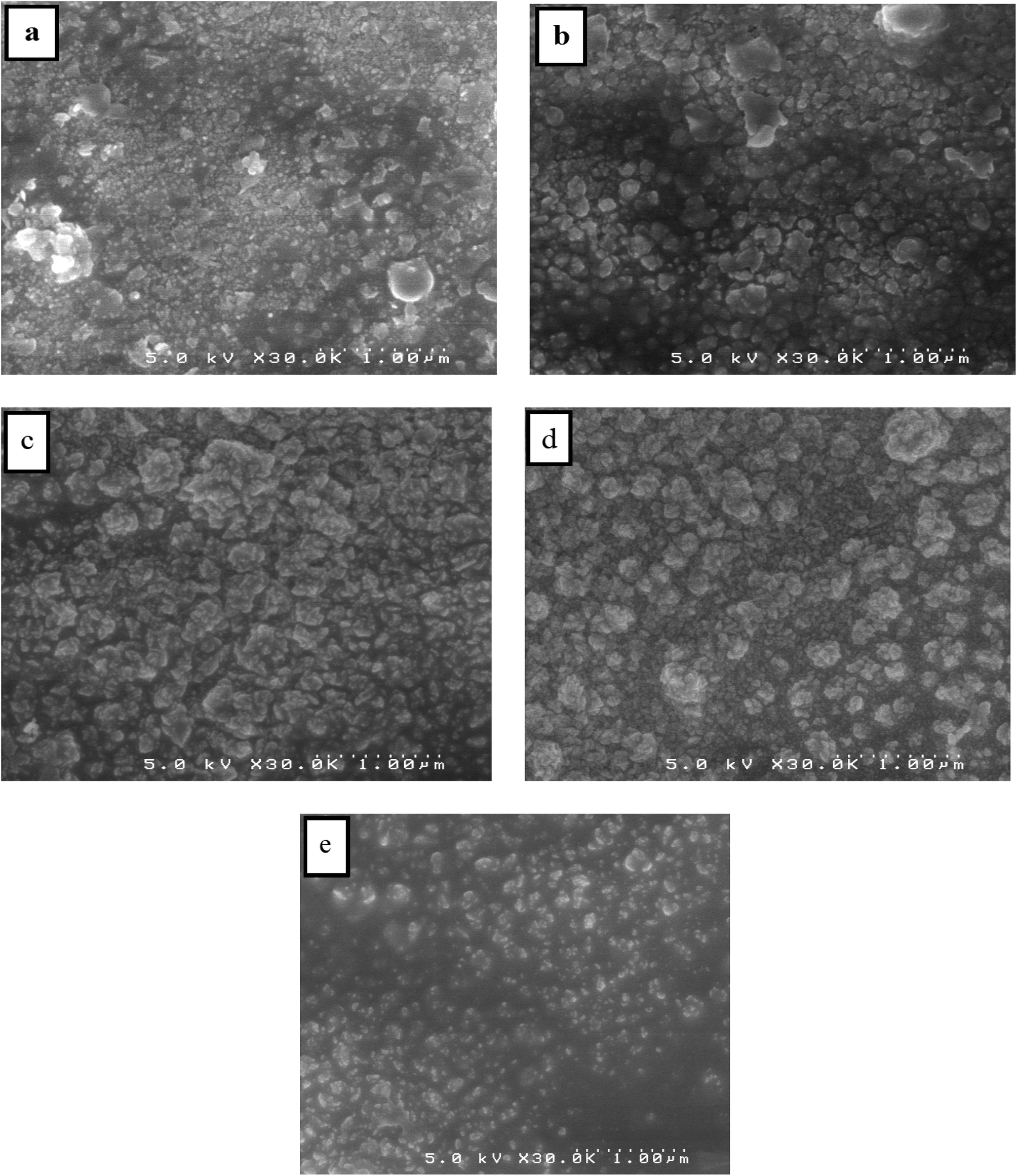 | ||
| Fig. 5 SEM images of (a) pure SnO2, (b) SnO2:Dy 1%, (c) SnO2:Dy 3%, (d) SnO2:Dy 5% and (e) SnO2:Dy 7% thin film samples. | ||
The thickness of the thin films is obtained by measuring the side surface width in the cross section of an SEM image. Fig. 6 presents the SEM cross-section images for pure and doped SnO2 thin films. Using this method, the average thickness of the different SnO2 layers was determined to be 237, 317.5, 364, 378 and 339 nm for the 0, 1, 3, 5, and 7% Dy-doped thin films, respectively. In addition, the images allowed us to clearly see the effect of Dy, as the thickness value increases as the doping percentage increases. These results confirm those calculated by means of the interference fringes method only for the 7% Dy-doped SnO2 thin film, whose error range is slightly greater at about ±30 nm. This slight difference does not detract from the effectiveness of the interference fringes method and is related to the inhomogeneous character of the porous surfaces produced via the spray method.
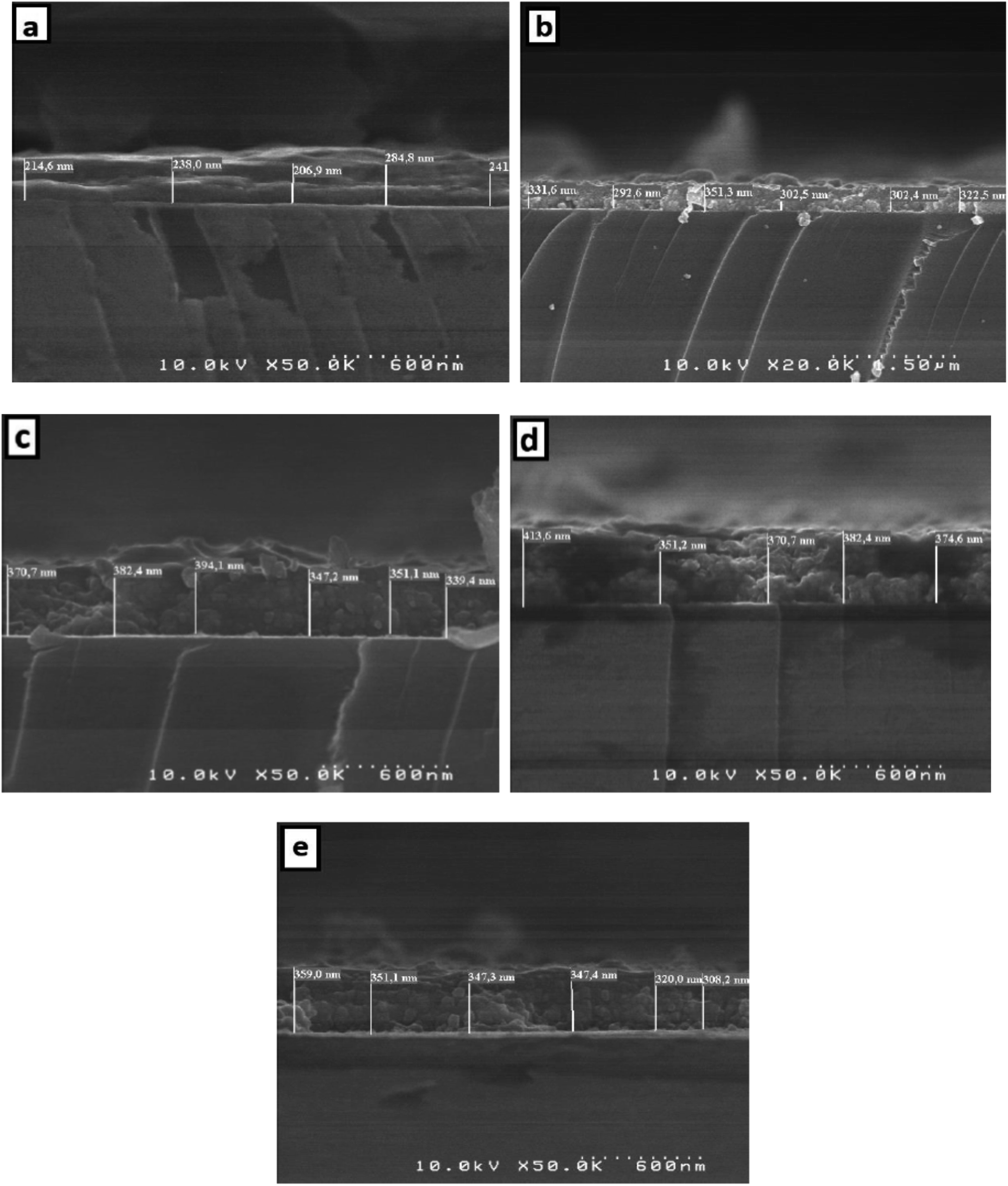 | ||
| Fig. 6 Cross-section of (a) pure SnO2, (b) SnO2:Dy 1%, (c) SnO2:Dy 3%, (d) SnO2:Dy 5% and (e) SnO2:Dy 7% thin film sample ESEM images. | ||
3.4 Chemical composition
Energy-dispersive X-ray spectroscopy (EDS) is used to determine the chemical composition of the pure and Dy-doped SnO2 thin films. The elemental compositions obtained using EDS are shown in Table 3. Analysis of this data reveals the presence of Dy, Sn, and O elements in accordance with atomic ratios obtained from the initial precursors for respective samples, as well as Si (with substrate contribution) with very low concentration traces of Mg, Al, Na, Cl, and Ca.| Spectrum | Sn | O | Dy | Si | Cl | Na | Mg | Al | Ca |
|---|---|---|---|---|---|---|---|---|---|
| SnO2 | 13.23 ± 0.60 | 57.23 ± 0.44 | 0.00 | 19.40 ± 0.66 | 1.57 ± 0.08 | 3.83 ± 0.29 | 1.07 ± 0.05 | 0.98 ± 0.03 | 2.67 ± 0.06 |
| SnO2:Dy 1% | 19.08 ± 0.79 | 56.10 ± 0.03 | 0.39 ± 0.01 | 14.68 ± 0.77 | 3.18 ± 0.40 | 2.33 ± 0.18 | 0.83 ± 0.06 | 1.06 ± 0.04 | 2.38 ± 0.10 |
| SnO2:Dy 3% | 21.27 ± 1.28 | 57.63 ± 0.23 | 0.95 ± 0.07 | 11.57 ± 1.4 | 3.55 ± 0.5 | 1.44 ± 0.24 | 0.58 ± 0.08 | 0.95 ± 0.01 | 2.06 ± 0.09 |
| SnO2:Dy 5% | 20.48 ± 1.23 | 57.67 ± 0.47 | 1.77 ± 0.11 | 11.90 ± 1.19 | 3.33 ± 0.25 | 1.32 ± 0.37 | 0.44 ± 0.17 | 0.92 ± 0.11 | 2.16 ± 0.12 |
| SnO2:Dy 7% | 20.78 ± 1.93 | 52.63 ± 0.78 | 2.58 ± 0.29 | 13.30 ± 1.92 | 5.43 ± 0.99 | 1.33 ± 0.57 | 0.36 ± 0.15 | 1.15 ± 0.13 | 2.44 ± 0.13 |
The correct levels of Dy are present in every layer. The high levels of O atoms are related to the experimental conditions, which included the use of H2O as a solvent.
3.5 Electrical properties
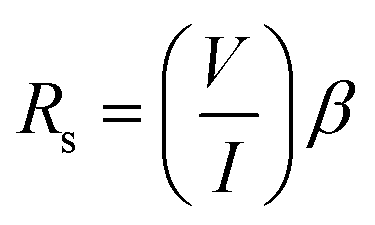
As illustrated in Fig. 7, a voltmeter was used to measure the voltage (V) across probes A and B while a high impedance (I) current source was utilized to deliver current through the two probes C and D. Eqn (13) was applied to the values of the observed voltages and sourced current to determine the bulk resistivity of the sample.61| Rb = Rs × t | (13) |
 | (14) |
 in the case of semi-infinite thin films.
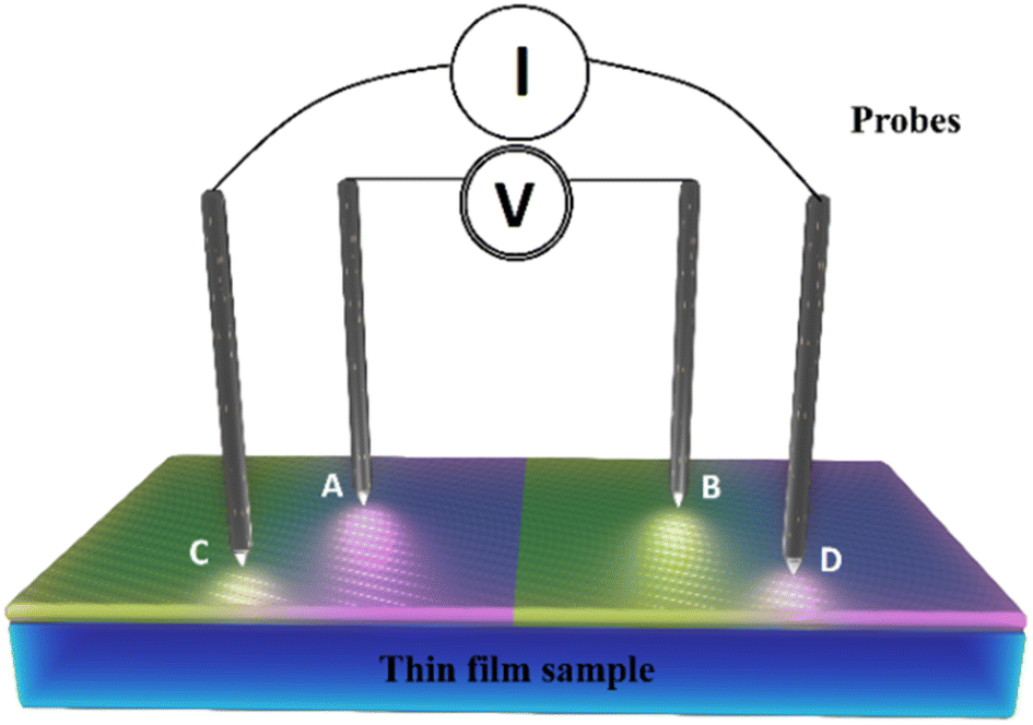 | ||
| Fig. 7 A diagram showing the four-point configuration used in taking the electrical measurements. | ||
The electrical resistance and resistivity values are listed in Table 4.
| Samples | Sheet resistance (Ω sq−1) | Electrical resistivity (×10−4 Ω cm) |
|---|---|---|
| SnO2 pure | 42.76 | 102.07 |
| SnO2:Dy 1% | 25.11 | 95.41 |
| SnO2:Dy 3% | 18.73 | 69.88 |
| SnO2:Dy 5% | 10.46 | 33.49 |
| SnO2:Dy 7% | 87.05 | 330.16 |
Fig. 8 shows the sheet resistivity for pure SnO2 and Dy-doped thin films. All samples show low sheet resistivity, due to the formation of oxygen vacancies, which function as electron donors and raise the concentration of free carriers. The undoped SnO2 thin films showed a low sheet resistivity of 102.07 × 10⁻⁴ Ω cm, which can be attributed to the divergence from stoichiometry.63 First, the sheet resistivity dropped until it reached a minimal value of 33.49 × 10⁻⁴ Ω cm for the Dy 5% as the dopant concentration increased. This is due to the presence of Dy3+ ions in the SnO2 crystal lattice, leading to an addition in the numbers of the free electrons and causing an increase in the concentration of free carriers.64 The sheet resistivity of the thin films increased after the minimum point as the dopant concentration is raised above the ideal doping level. This is because the crystal structure of the thin film began to degenerate when the dysprosium atoms inserted themselves into the interstitial spaces, which resulted in a decrease in the mobility of free charge carriers and an increase in the sheet resistivity of the thin films. Similar results were obtained by Patrick and al., who examined the effect of Pd doping on SnO2 thin layers.65
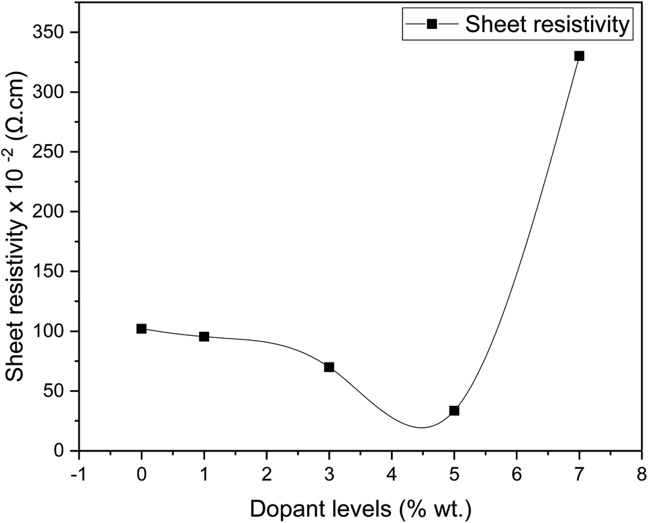 | ||
| Fig. 8 Variation of resistivity in sheet characteristics of SnO2:Dy by Dy levels. | ||
3.6 Photocatalytic activity
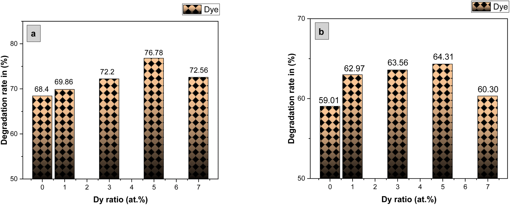
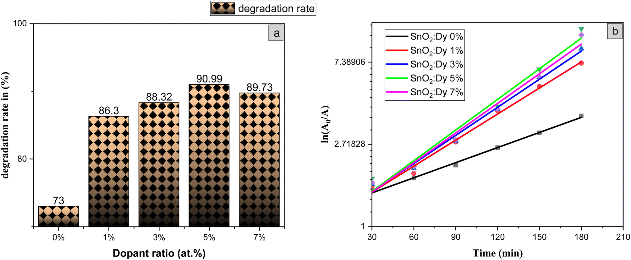
The photocatalytic activity of the undoped and Dy-doped SnO2 thin films is evaluated using the degradation of methylene blue (MB). This organic dye exhibits a strong absorbance band at 660 nm whose intensity decreases as the MB degrades. Variations in intensity were assessed at regular time intervals. Fig. 11 shows the spectra of the degradation rate of MB after solar irradiation for three hours using the Dy-doped SnO2 thin films at various Dy concentrations under solar irradiation.The diagrams in Fig. 14a demonstrate the good photocatalytic responses of pure and Dy-doped SnO2 thin films. MB photo degradation rates were about 85% at three hours under sunlight for all doped thin films. Furthermore, by calculating the degradation efficiency given by eqn (1), we were able to confirm the efficiency of the thin films through the degradation of the MB dye, which increased when the Dy doping level increased to reach 90.99% for 5% Dy, proving that the dopant caused the degradation mechanism. This effect is highest for the 5% doped thin films, which can be attributed to a higher number of free electrons (these samples show the highest conductivity) to powerfully activate the degradation activity, as well as to the band gap reaching the visible range, which enhanced the absorption of the sunlight irradiation. This is comparable to other results, and this low-cost approach could offer a flexible means of enhancing the photocatalytic activity of SnO2 to high levels of efficiency.
Table 5 provides some examples of the photocatalytic efficiency of SnO2, either doped or coupled with other materials, that has attracted the attention of many researchers:
| Coupled and doped catalyst | Light source/dye | Photodegradation efficiency | Ref. |
|---|---|---|---|
| SnO2:Zn | Visible annular brand photoreactor (UV)/MB | Efficiency ranges from 68 to 90% | 66 |
| SnO2/Fe | 250 W UV light/rhodamine B | Degraded RhB solution by w55% | 67 |
| SnO2/Co | 450 W Hg lamp/4-hydroxy benzoic acid | Complete photodegradation of 4-HBA | 68 |
| Graphene/SnO2 | 350 W Xe lamp sunlight/MB | Dye was degraded completely after 6 h | 69 |
| SnO2:Tb | UV lamp (λ = 254 nm)/(MB) | Efficiency goes from 72 to 85% | 70 |
| SnO2:Dy | Solar irradiation/MB | 90.99% | Our work |
To more clearly observe the effect of Dy doping on the photocatalytic activity of the thin films, the kinetic rate (K) is calculated using this formula:71
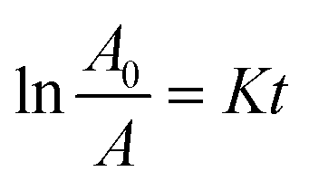 | (15) |
The slope of the ln(A/A0) vs. irradiation time (t) plot yields the constant rate K (Fig. 14b). The results shows that the reaction rate constant increased as the doping concentration increased with a higher value of K for thin films doped at 5%, demonstrating that the addition of Dy to SnO2 at several levels improves photocatalytic activity under solar irradiation.
• Study of stability and reusability
Three consecutive cycles of methylene blue (MB) degradation were carried out under solar irradiation, as depicted in the Fig. 9, to evaluate the sustained effectiveness of SnO2:Dy samples with a dye concentration of 3 mg L−1. After each cycle, the samples underwent a thorough washing process, involving multiple rinses with distilled water, followed by drying at 50 °C. Remarkably, only a minor decrease in photocatalytic efficiency, estimated at approximately 10%, is observed after each cycle. This highlights the remarkable resilience of Dy-doped SnO2 thin films in the degradation of methylene blue. It should be noted that the effectiveness of SnO2 in photocatalyzing methylene blue may vary depending on the specific experimental conditions or application.
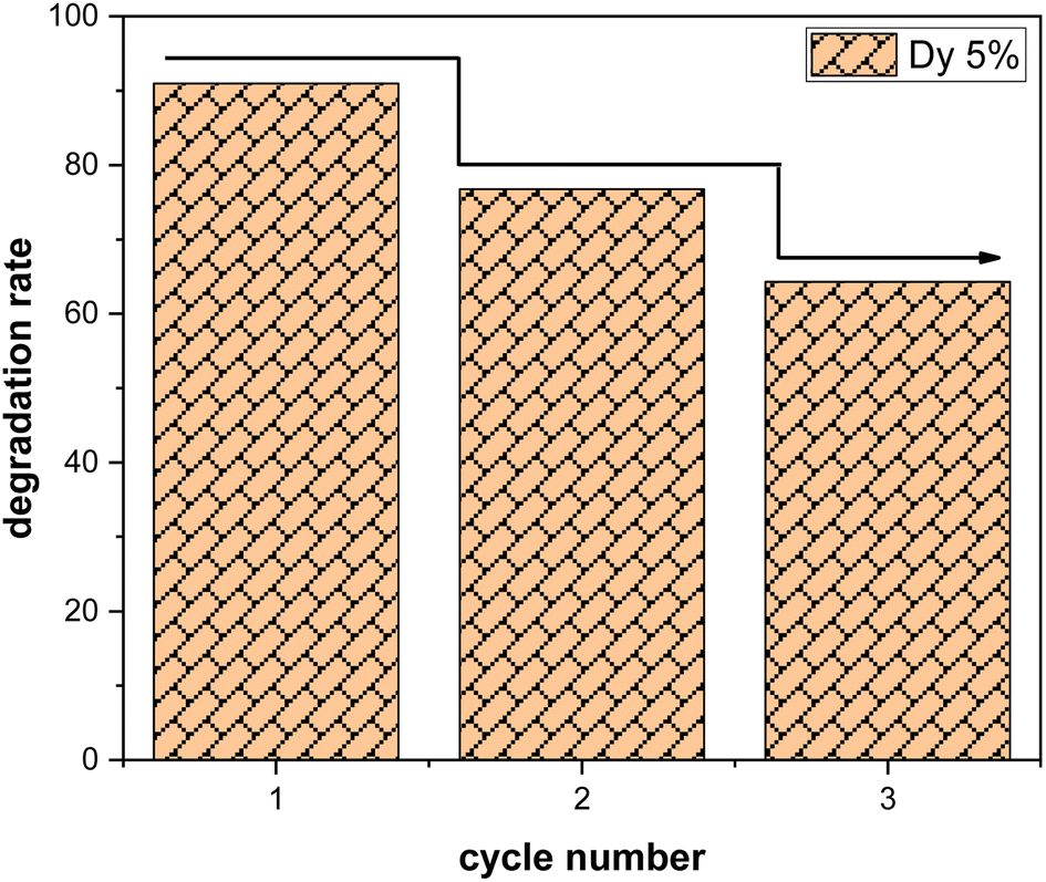 | ||
| Fig. 9 Recyclability of Dy doped SnO2 at 5%. | ||
• Effect of MB dye concentration
The influence of methylene blue (MB) concentrations on the photocatalytic degradation process was investigated by varying MB concentrations from 2 mg L−1 to 4 mg L−1, with a 1 mg L−1 increment, while exposing the system to solar light irradiation as shown in Fig. 11. Fig. 10 illustrates the results. It was observed that the rate of MB degradation is highly efficient for concentrations up to 3 mg L−1. However, when the concentration exceeded 3 mg L−1 and reached 4 mg L−1, the rate of MB photodegradation slowed down, ultimately reaching only 41% degradation over a 3 hour period.This behavior can be attributed to increased competition between MB molecules for degradation and a decrease in the intensity of light reaching the surface of the SnO2 photocatalyst. At higher concentrations, the solution effectively screens a significant portion of the incoming light, allowing fewer photons to reach the SnO2 surface. Consequently, the production of electron–hole pairs, which are crucial for the degradation process, is significantly reduced. This reduction in electron–hole pairs, in turn, leads to a decrease in the degradation of the dye.72
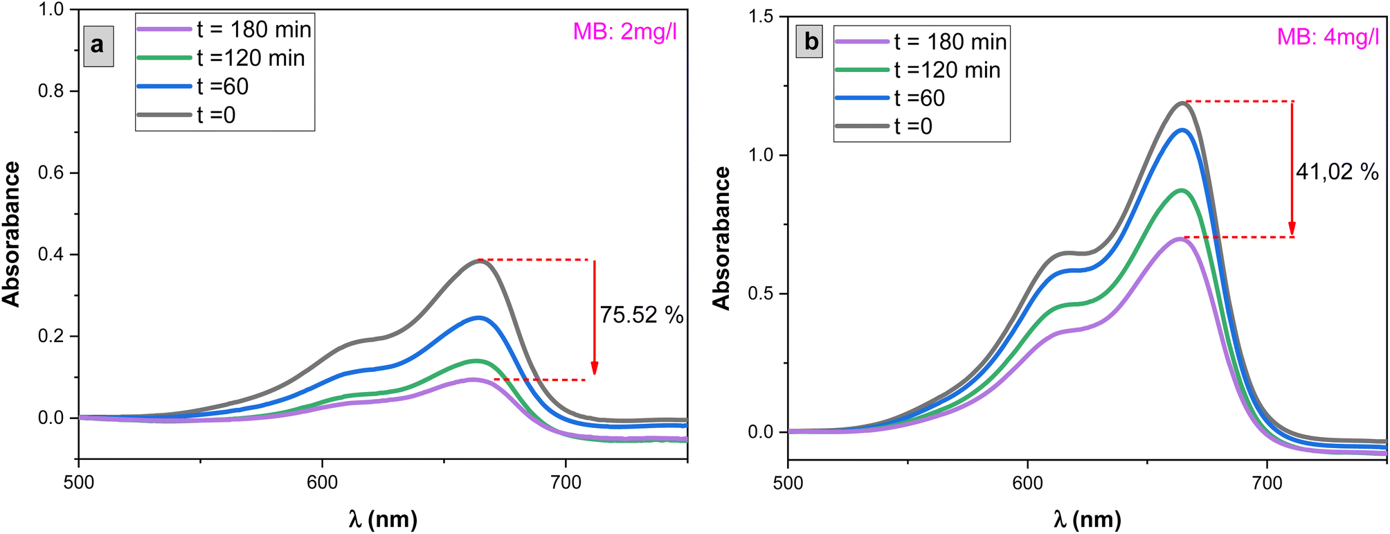 | ||
| Fig. 10 Degradation of MB dye versus irradiation time in the presence of sprayed SnO2:Dy [0, 1, 3, 5 and 7% at.] thin films with concentration of MB with MB concentrations (a) 2 mg L−1 and (b) 4 mg L−1. | ||
 | ||
| Fig. 11 Degradation rate of MB in presence of the Dy-doped SnO2 thin films at various Dy ratios (0, 1, 3, 5 and 7% at.) for 3 hours under solar irradiation with MB concentrations (a) 2 mg L−1 and (b) 4 mg L−1. | ||
• Mechanism of photocatalytic degradation
Much research has focused on better understanding the process of photocatalysis. It involves a sequence of reduction and oxidation reactions, where the electrons move from the valence band (VB) to the conduction band (CB), simultaneously generating oxidative valence holes (h+) and reductive conduction electrons (e), generally activated when the energy of the light irradiation is equal to or higher than the energy band gap of the catalyst (eqn (16)). In a redox reaction, which involves both electrons and holes, the excited conduction band electrons (eCB) are captured by oxygen molecules, creating reactive peroxide radicals (˙O2−) eqn (17). Hydroxyl radicals are then created when (hVB+) and the water (H2O) that has been adsorbed react on the surface of the thin film producing (OH˙), as shown in eqn (18).
Various dopants have been used to improve the effectiveness of photocatalytic reactions and decrease the process of hole and electron recombination. Rare earth dopants have been found to be one of the most effective materials for acting as trapping sites to slow down the recombination process and extend the mean lifetime.73 The doping procedure causes the trapped charges to be transported to the film's surface where they interact with the dye molecules to boost photocatalytic efficiency.74 In our case, dysprosium also has a potent 4f orbital that is partially occupied, making it a Lewis acid that may quickly react with electrons from the conduction band.75
According to eqn (24), a small number of (OH) radicals rearrange to create H2O2, which then dissociates into (OH) radicals as shown in eqn (25). Finally, the breakdown of the organic contaminants is demonstrated in eqn (26) by the hydroxyl radicals produced by the photocatalysis processes (Fig. 13).
| SnO2 + hν → SnO2 (eCB−) + SnO2 (hVB+) | (16) |
| SnO2 (eCB−) + O2 → ˙O2− | (17) |
| O2− + e− + 2H+ → H2O2 | (18) |
| Dy3+ + eCB− → Dy2+ | (19) |
| Dy2+ + O2(ads) → O2− | (20) |
| O2− + H + → HO2 | (21) |
| H2O2 + e− → OH + OH− | (22) |
| SnO2 (hVB+) + H2O → ˙OH + H+ | (23) |
| SnO2 + UVirradiation + H2O → ˙H + ˙OH | (24) |
| H+ + OH˙ → HO˙ | (25) |
| OH + methylene blue dye → CO2 + H2O + degraded products | (26) |
The mechanism of the photodegradation of MB is simplified in Fig. 12.
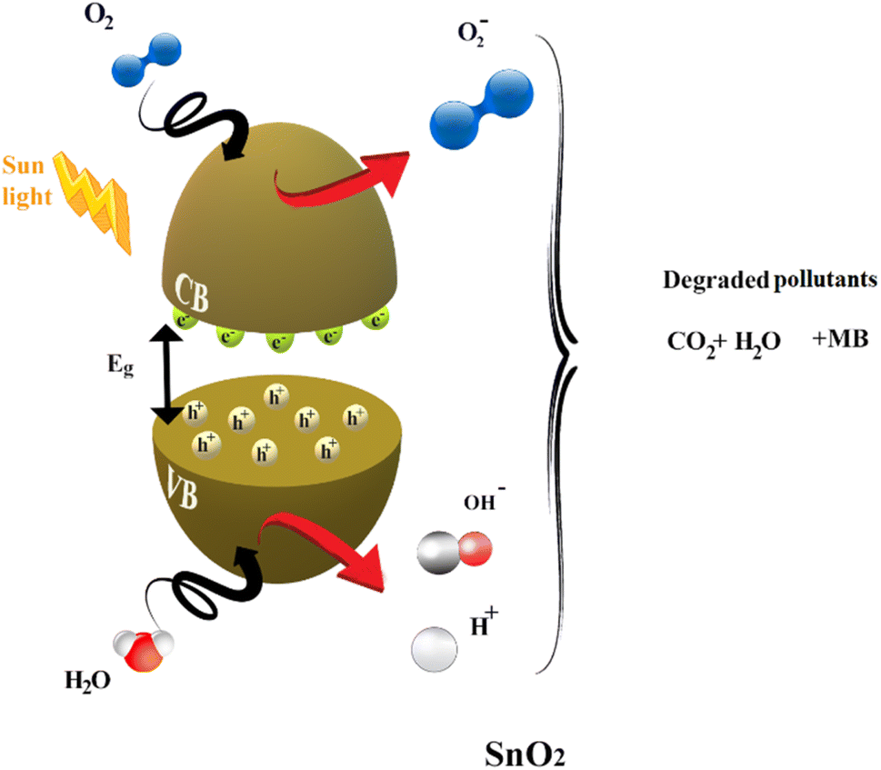 | ||
| Fig. 12 Mechanism of photodegradation of MB by SnO2 thin films under solar irradiation. | ||
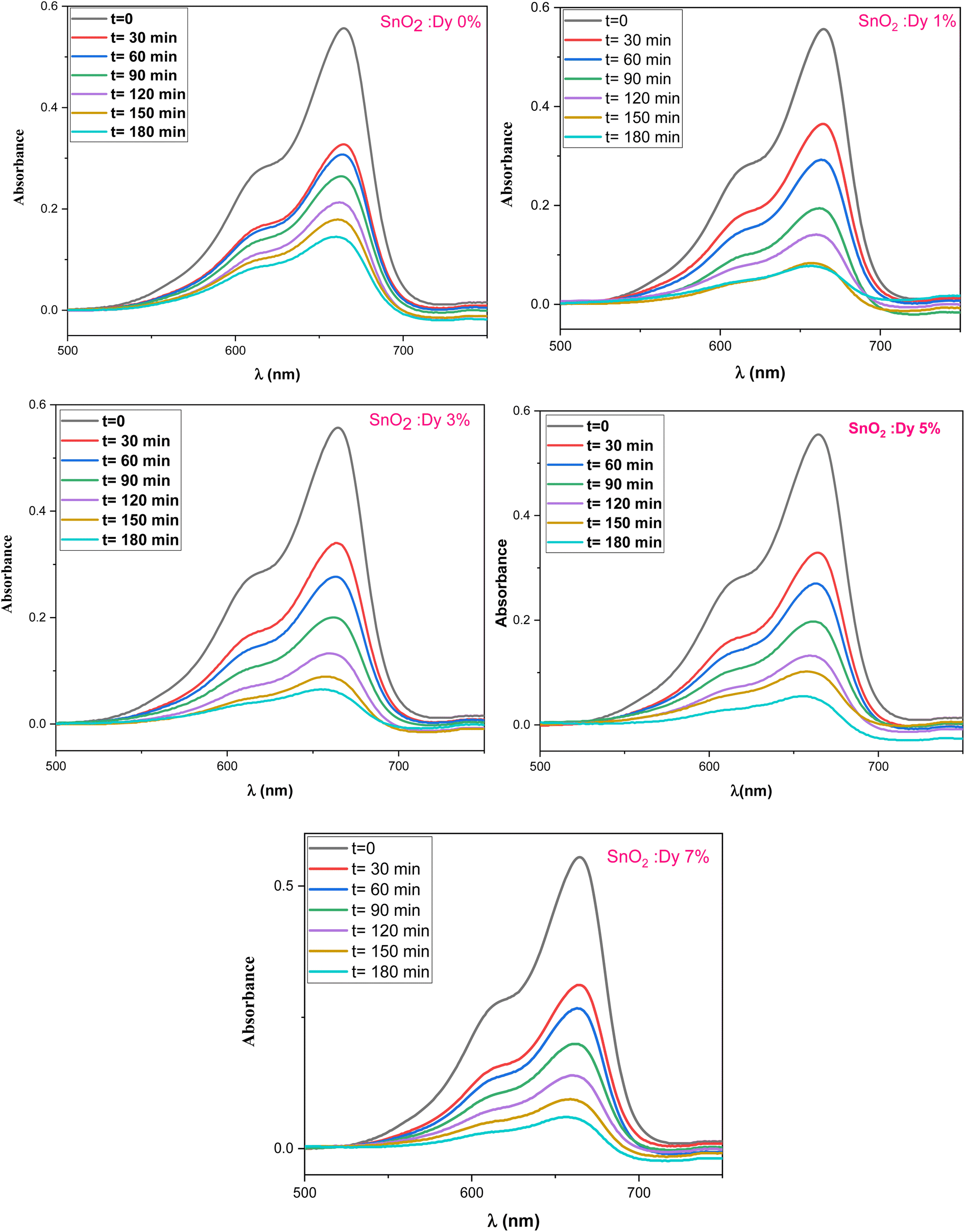 | ||
| Fig. 13 Degradation of MB dye versus irradiation time in the presence of sprayed SnO2:Dy [0, 1, 3, 5 and 7% at.] thin films. | ||
 | ||
| Fig. 14 (a) Degradation rate of MB in presence of the Dy-doped SnO2 thin films at various Dy ratios (0, 1, 3, 5 and 7% at.) for 3 hours under solar irradiation, (b) graphic determination of the kinetic rate K as a function of Dy content. | ||
Better photocatalytic activity can result from the overlap of a variety of factors like the higher electron mobility and charge carrier concentration of the samples and the right choice of doping materials at the right concentration levels. Other keys to achieving better results may include the synergistic effect on the adsorption phenomenon and the extended charge separation resulting from the interface of the photocatalyst species following charge transfer between two semiconducting materials, as well as intrinsic defects like oxygen vacancies that favor the interfacial charge transfer in their role as trapping centers of the photogenerated electrons and preventers of the electron–hole recombination.
4 Conclusions
Pure and dysprosium-doped SnO2 thin films were successfully synthesized on glass substrate using the spray pyrolysis technique. In order to obtain high-quality thin films, the impact of various dysprosium rates, which were examined by means of several different characterizations, was studied. XRD analyses revealed a tetragonal rutile structure for the SnO2:Dy thin films, with a better crystallization for the SnO2:Dy 5% thin films. The optical study showed that the materials used have high transparency levels and the optical gap decreases from 3.91 to 3.56 eV with an increase in the doping rate. SEM images showed an enhancement in the structure of the surface with an increase in the density of the grain to reach the maximum with SnO2:Dy 5%. In addition, sheet resistivity exhibited low values that decreased as the doping rates increased, reaching a minimum of 33.49 × 10⁻² Ω cm for the 5% doped thin layers, which increased considerably for the 7% doped thin films. These results are confirmed by the destruction of the structure shown in the SEM images. Although methylene blue photodegradation showed high levels, reaching 90% in three hours under solar irradiation for the 5% Dy-doped SnO2 thin films, the cooperation of all these properties makes SnO2:Dy thin films good candidates for use in the field of photocatalytic applications such as wastewater treatment.Conflicts of interest
There are no conflicts to declare.Acknowledgements
The authors are grateful to Professor Eric AUBRY and Pascal BRIOIS for their help in providing electric and EDS characterizations. E. L. is supported by the Catalan Institution for Research and Advanced Studies via the 2018 Edition of the ICREA Academia Award.References
- S. Benkhaya, S. M'rabet and A. El Harfi, A review on classifications, recent synthesis and applications of textile dyes, Inorg. Chem. Commun., 2020, 115, 107891 CrossRef CAS.
- A. I. Abd-Elhamid, M. Emran, M. H. El-Sadek, A. A. El-Shanshory, H. M. A. Soliman, M. A. Akl and M. Rashad, Enhanced removal of cationic dye by eco-friendly activated biochar derived from rice straw, Appl. Water Sci., 2020, 10, 45 CrossRef CAS.
- M. Ahmad, W. Rehman, M. M. Khan, M. T. Qureshi, A. Gul, S. Haq, R. Ullah, A. Rab and F. Menaa, Phytogenic fabrication of ZnO and gold decorated ZnO nanoparticles for photocatalytic degradation of Rhodamine B, J. Environ. Chem. Eng., 2021, 9, 104725 CrossRef CAS.
- H. D. Bouras, Z. Isik, E. B. Arikan, A. R. Yeddou, N. Bouras, A. Chergui, L. Favier, A. Amrane and N. Dizge, Biosorption characteristics of methylene blue dye by two fungal biomasses, Int. J. Environ. Stud., 2020, 78, 365–381 CrossRef.
- S. Pandey, J. Y. Do, J. Kim and M. Kang, Fast and highly efficient removal of dye from aqueous solution using natural locust bean gum based hydrogels as adsorbent, Int. J. Biol. Macromol., 2020, 143, 60–75 CrossRef CAS PubMed.
- Z. Derakhshan, M. A. Baghapour, M. Ranjbar and M. Faramarzian, Adsorption of Methylene Blue Dye from Aqueous Solutions by Modified Pumice Stone: Kinetics and Equilibrium Studies, Health Scope, 2013, 2, 136–144 CrossRef.
- F. N. Allouche and N. Yassaa, Potential adsorption of methylene blue from aqueous solution using green macroalgae Posidonia oceanica, in Proceedings of the IOP Conference Series: Materials Science and Engineering, International Conference on Functional Materials and Chemical Engineering (ICFMCE 2017), Dubai, UAE, 2017, vol. 323012006 CrossRef CAS; T. H. Han, M. M. Khan, S. Kalathil, J. Lee and M. H. Cho, Simultaneous enhancement of methylene blue degradation and power generation in a microbial fuel cell by gold nanoparticles, Ind. Eng. Chem. Res., 2013, 52, 8174–8181 CrossRef CAS.
- M. Rafatullah, O. Sulaiman, R. Hashim and A. Ahmad, Adsorption of methylene blue on low-cost adsorbents: a review, J. Hazard. Mater., 2010, 177, 70–80 CrossRef CAS PubMed.
- S. Sahu, S. Pahi, J. K. Sahu, U. K. Sahu and R. K. Patel, Kendu (Diospyros melanoxylon Roxb) fruit peel activated carbon—an efficient bioadsorbent for methylene blue dye: equilibrium, kinetic, and thermodynamic study, Environ. Sci. Pollut. Res., 2020, 27, 22579–22592 CrossRef CAS PubMed.
- M. Makeswari and P. Saraswathi, Photo catalytic degradation of methylene blue and methyl orange from aqueous solution using solar light onto chitosan bi-metal oxide composite, SN Appl. Sci., 2020, 2, 336 CrossRef CAS.
- S. Sabar, H. Abdul Aziz, N. H. Yusof, S. Subramaniam, K. Y. Foo, L. D. Wilson and H. K. Lee, Preparation of sulfonated chitosan for enhanced adsorption of methylene blue from aqueous solution, React. Funct. Polym., 2020, 151, 104584 CrossRef CAS.
- J. Cheng, C. Zhan, J. Wu, Z. Cui, J. Si, Q. Wang, X. Peng and L. S. Turng, Highly Efficient Removal of Methylene Blue Dye from an Aqueous Solution Using Cellulose Acetate Nanofibrous Membranes Modified by Polydopamine, ACS Omega, 2020, 5, 5389–5400 CrossRef CAS PubMed.
- X. Wei, Y. Wang, Y. Feng, X. Xie, X. Li and S. Yang, Different adsorption-degradation behavior of methylene blue and Congo red in nanoceria/H2O2 system under alkaline conditions, Sci. Rep., 2019, 9, 4964 CrossRef PubMed.
- M. Rafatullah, O. Sulaiman, R. Hashim and A. Ahmad, Adsorption of methylene blue on low-cost adsorbents: a review, J. Hazard. Mater., 2010, 177, 70–80 CrossRef CAS PubMed.
- E. Santoso, R. Ediati, Y. Kusumawati, H. Bahruji, D. O. Sulistiono and D. Prasetyoko, Review on recent advances of carbon based adsorbent for methylene blue removal from waste water, Mater. Today Chem., 2020, 16, 100233 CrossRef CAS.
- F. Mashkoor and A. Nasar, Magsorbents: Potential candidates in wastewater treatment technology—A review on the removal of methylene blue dye, J. Magn. Magn. Mater., 2020, 500, 166408 CrossRef CAS.
- A. Sahibed-dine, F. Bentiss and M. Bensitel, The photocatalytic degradation of methylene blue over TiO2 catalysts supported on hydroxyapatite, J. Mater, 2017, 8(4), 1301–1311 Search PubMed.
- T. Al-Garni, et al., Synthesis of ZnO Nanoparticles by using Rosmarinus officinalis Extract and their Application for Methylene blue and Crystal violet Dyes Degradation under Sunlight irradiation, 2021 Search PubMed.
- V. Janakiraman, et al., Structural, optical and morphological properties of Ta 2O5/SnO2 nanocomposite thin film prepared by spray pyrolysis method, J. Mater. Sci.: Mater. Electron., 2021, 32, 9244–9252 CrossRef CAS.
- P.-P. Filippatos, et al., Impact of boron and indium doping on the structural, electronic and optical properties of SnO2, Sci. Rep., 2021, 11, 13031 CrossRef CAS PubMed.
- W. Zhang, et al., Highly sensitive and low operating temperature SnO2 gas sensor doped by Cu and Zn two elements, Sens. Actuators, B, 2017, 243, 982–989 CrossRef CAS.
- Z. Zhang, et al., Preparation of a novel Ni/Sb co-doped Ti/SnO2 electrode with carbon nanotubes as growth template by electrodeposition in a deep eutectic solvent, J. Electroanal. Chem., 2022, 911, 116225 CrossRef CAS.
- H. He, et al., Novel p-type conductivity in SnO2 thin films by Mg doping, J. Alloys Compd., 2017, 714, 258–262 CrossRef CAS.
- A. S. Ibrahim, et al., Influence of Cu doping on structure, morphology and optical characteristics of SnO2 thin films prepared by chemical bath deposition technique, Opt. Mater., 2021, 117, 111212 CrossRef.
- M. S. Najihah, et al., Effect of Ni-doping on properties of the SnO2 synthesized using Tradescantia spathacea for photoantioxidant studies, Mater. Chem. Phys., 2020, 252, 123293 CrossRef.
- L. Wang, et al., Mo-doped SnO2 nanotubes sensor with abundant oxygen vacancies for ethanol detection, Sens. Actuators, B, 2021, 347, 130642 CrossRef CAS.
- D. Toloman, et al., Enhanced photocatalytic activity of Co doped SnO2 nanoparticles by controlling the oxygen vacancy states, Opt. Mater., 2020, 110, 110472 CrossRef CAS.
- A. Al-Hamdi and M. Sillanpää, Photocatalytic activities of antimony, iodide, and rare earth metals on SnO2 for the photodegradation of phenol under UV, solar, and visible light irradiations, Adv. Water Treat., 2020, 129–288 Search PubMed.
- J. Song, et al., Colloidal synthesis of Y-doped SnO2 nanocrystals for efficient and slight hysteresis planar perovskite solar cells, Sol. Energy, 2019, 185, 508–515 CrossRef CAS.
- F. Hild, et al., Structural and photoluminescence properties of evaporated SnO2 thin films doped with rare earths, Energy Procedia, 2015, 84, 141–148 CrossRef CAS.
- I. Raj, et al., Study on the synergistic effect of terbium-doped SnO2 thin film photocatalysts for dye degradation, J. Nanopart. Res., 2020, 22(12), 1–14 CrossRef.
- H. Rinnert, et al., Photoluminescence of Nd-doped SnO2 thin films, Appl. Phys. Lett., 2012, 100(10), 101908 CrossRef.
- S. Deepa, P. Kumari Krishnan and B. Thomas, Spray Pyrolyzed Praseodymium Doped SnO2 Thin Film with Fast Response to LPG: Analysis Based on Microstructural Features, Key Eng. Mater., 2022, 934, 23–36 Search PubMed.
- I. L. P. Raj, M. S. Revathy and A. J. Christy, et al., Study on the synergistic effect of terbium-doped SnO2 thin film photocatalysts for dye degradation, J. Nanopart. Res., 2020, 22, 359, DOI:10.1007/s11051-020-05084-2.
- M. Ayadi, et al., Effect of cerium doping on the structural, optical and photocatalytic properties of SnO2 thin films prepared by spray pyrolysis method, Mater. Res. Express, 2019, 6, 076407 CrossRef CAS.
- M. Dhiman and S. Singhal, Effect of doping of different rare earth (europium, gadolinium, dysprosium and neodymium) metal ions on structural, optical and photocatalytic properties of LaFeO3 perovskites, J. Rare Earths, 2019, 37(12), 1279–1287, DOI:10.1016/j.jre.2018.12.015.
- F. Abbas and R. Bensaha, Effect of annealing time on structural and optical proprieties of mercury (Hg+ 2) doped TiO2 thin films elaborated by sol-gel method for future photo-catalytic application, Optik, 2021, 247, 167846 CrossRef CAS.
- G. El Fidha, et al., Physical and photocatalytic properties of sprayed Dy doped ZnO thin films under sunlight irradiation for degrading methylene blue, RSC Adv., 2021, 11, 24917–24925 RSC.
- S. K. Pillai, L. M. Sikhwivhilu and T. K. Hillie, Synthesis, characterization and photoluminescence properties of Dy3+-doped nano-crystalline SnO2, Mater. Chem. Phys., 2010, 120, 619–624 CrossRef CAS.
- T. C. Paul, et al., Influence of Fe3+ ions doping on TiO2 thin films: Defect generation, dd transition and band gap tuning for optoelectronic device applications, Phys. B, 2021, 604, 412618 CrossRef CAS.
- M. Miki-Yoshida, J. Morales and J. Solis, Influence of Al, In, Cu, Fe and Sn dopants on the response of thin film ZnO gas sensor to ethanol vapour, Thin Solid Films, 2000, 373, 137–140 CrossRef.
- P. Sivakumar, et al., Influence of Ga doping on structural, optical and electrical properties of transparent conducting SnO2 thin films, Optik, 2021, 226, 165859 CrossRef CAS.
- I. Arora, et al., Structural, optical and electrical characterization of spin coated SnO2: Mn thin films, Mater. Today: Proc., 2021, 36, 697–700 CrossRef CAS.
- Md F. Hossain, et al., Transparent conducting SnO2 thin films synthesized by nebulized spray pyrolysis technique: Impact of Sb doping on the different physical properties, Mater. Sci. Semicond. Process., 2021, 121, 105346 CrossRef CAS.
- M. M. Kareem, Z. T. Khodair and F. Y. Mohammed, Effect of annealing temperature on Structural, morphological and optical properties of ZnO nanorod thin films prepared by hydrothermal method, J. Ovonic Res., 2020, 16, 53–61 CrossRef.
- Z. T. Khodair, et al., Study of optical and structural properties of (NiO) 1-x (CuO) x nanostructures thin films, Chem. Data Collect., 2020, 28, 100414 CrossRef CAS.
- S. Saha and V. Gupta, Al and Fe co-doped transparent conducting ZnO thin film for mediator-less biosensing application, AIP Adv., 2011, 1, 042112 CrossRef.
- M. Kumar, A. Kumar and A. C. Abhyankar, Influence of texture coefficient on surface morphology and sensing roperies of W-doped nanocrystalline tin oxide thin films, ACS Appl. Mater. Interfaces, 2015, 7, 3571–3580 CrossRef CAS PubMed.
- U. Farva and J. Kim., Growth temperature-dependent morphological, optical, and electrical study of SnO2 thin film by atomic layer deposition, Mater. Chem. Phys., 2021, 267, 124584 CrossRef CAS.
- B. Mallesham, S. Roy, S. Bose, A. N. Nair, S. Sreenivasan, V. Shutthanandan and C. V. Ramana, Crystal Chemistry, Band-Gap Red Shift, and Electrocatalytic Activity of Iron-Doped Gallium Oxide Ceramics, ACS Omega, 2019, 9b01604, DOI:10.1021/acsomega.
- M. Shkir, et al., Influence of Dy doping on key linear, nonlinear and optical limiting characteristics of SnO2 films for optoelectronic and laser applications, Opt Laser. Technol., 2018, 108, 609–618 CrossRef CAS.
- R. Balakarthikeyan, et al., Performance analysis of SnS thin films fabricated using thermal evaporation technique for photodetector applications, Optik, 2021, 244, 167460 CrossRef CAS.
- A. P. Sreekala, et al., AgSbS2-xSex thin films: structure, composition, morphology and photodetection properties, Mater. Today Commun., 2021, 27, 102362 CrossRef.
- Z. Zarhri, et al., Optical measurements and Burstein Moss effect in optical properties of Nb-doped BaSnO3 perovskite, Micro Nanostruct., 2022, 166, 207223 CrossRef CAS.
- S. Palanichamy, et al., Physical properties of rare earth metal (Gd3+) doped SnO2 thin films prepared by simplified spray pyrolysis technique using nebulizer, Optik, 2019, 194, 162887 CrossRef.
- J. J. Cordell, et al., Band gap analysis and carrier localization in cation-disordered ZnGeN2, APL Mater., 2022, 10, 011112 CrossRef CAS.
- T. Gnanasekar, et al., Fabrication of Er, Tb doped CuO thin films using nebulizer spray pyrolysis technique for photosensing applications, Opt. Mater., 2022, 123, 111954 CrossRef CAS.
- J. Tauc, Optical Properties of Amorphous Semiconductors, in Amorphous and Liquid Semiconductors ed. Tauc, J., Springer, Boston, MA, 1974, DOI:10.1007/978-1-4615-8705-7_4.
- K. Derrar, M. Zaabat, A. Hafdallah, N. Rouabah, b. Gasmi and I. Zerrouk, Optical and structural properties of SnO2 thin films deposited by spray pyrolysis technique: effect of solution concentration, Defect Diffus. Forum, 2019, 397, 179–186 Search PubMed.
- H. Guan, et al., Structural and optical properties of Cu2FeSnS4 thin film synthesized via a simple chemical method, Mater. Sci. Semicond. Process., 2014, 25, 159–162 CrossRef CAS.
- B. Benhaoua, S. Abbas, A. Rahal, A. Benhaoua and M. S. Aida, Effect of film thickness on the structural, optical and electrical properties of SnO2: F thin films prepared by spray ultrasonic for solar cells applications, Superlattice, Microst, 2015, 83, 78–88 CrossRef CAS.
- P. Sivakumar, et al., Effect of Ti doping on structural, optical and electrical properties of SnO2 transparent conducting thin films deposited by sol-gel spin coating, Opt. Mater., 2021, 113, 110845 CrossRef CAS.
- V. K. Jain, P. Kumar and Y. K. Vijay, Preparation of nanostructure ZnO-SnO2 thin films for optoelectronic properties and post annealing influence, World Acad. Sci. Eng. Technol., 2012, 72, 1575–1577 Search PubMed.
- P. Sivakumar, et al., Effect of Ti doping on structural, optical and electrical properties of SnO2 transparent conducting thin films deposited by sol-gel spin coating, Opt. Mater., 2021, 113, 110845 CrossRef CAS.
- P. Mwathe, et al., Effect of surface passivation on electrical properties of Pd-F: SnO2 thin films prepared by spray pyrolysis technique, Coatings, 2014, 4, 747–755 CrossRef.
- S. Kumaravelan, et al., Effect of Zn dopant on SnO2 nano-pyramids for photocatalytic degradation, Chem. Phys. Lett., 2021, 769, 138352 CrossRef CAS.
- M. Davis, F. Hung-Low, W. M. Hikal and L. J. Hope-Weeks, Enhanced photocatalytic performance of Fe-doped SnO2 nanoarchitectures under UV irradiation: synthesis and activity, J. Mater. Sci., 2013, 48, 6404e6409 CrossRef.
- T. Entradas, J. F. Cabrita, S. Dalui, M. R. Nunes, O. C. Monteiro and A. J. Silvestre, Synthesis of sub-5 nm Co-doped SnO2 nanoparticles and their structural, microstructural, optical and photocatalytic properties, Mater. Chem. Phys., 2014, 147, 563e571 CrossRef.
- H. Seema, K. C. Kemp, V. Chandra and K. S. Kim, GrapheneeSnO2 composites for highly efficient photocatalytic degradation of methylene blue under sunlight, Nanotechnology, 2012, 23, 355705 CrossRef PubMed.
- I. L. P. Raj, M. S. Revathy, A. J. Christy, N. Chidhambaram, V. Ganesh and S. AlFaify, Study on the synergistic effect of terbium-doped SnO2 thin film photocatalysts for dye degradation, J. Nanopart. Res., 2020, 22, 1–14 CrossRef.
- M. R. Dustgeer, S. Tasmia and A. Jilani, et al., Synthesis and characterization of a novel single-phase sputtered Cu2O thin films: Structural, antibacterial activity and photocatalytic degradation of methylene blue, Inorg. Chem. Commun., 2021, 128, 108606 CrossRef CAS.
- K. Prakash, et al., Controllable synthesis of SnO2 photocatalyst with superior photocatalytic activity for the degradation of methylene blue dye solution, J. Exp. Nanosci., 2016, 11, 1138–1155 CrossRef CAS.
- T. Aitasalo, et al., Persistent luminescence phenomena in materials doped with rare earth ions, J. Solid State Chem., 2003, 171, 114–122 CrossRef CAS.
- I. L. P. Raj, et al., Significance of Ni doping on structure-morphology-photoluminescence, optical and photocatalytic activity of CBD grown ZnO nanowires for opto-photocatalyst applications, Inorg. Chem. Commun., 2020, 119, 108082 CrossRef.
- S. K. Gupta, K. Sudarshan and R. M. Kadam, Optical nanomaterials with focus on rare earth doped oxide: A Review, Mater. Today Commun., 2021, 27, 102277 CrossRef CAS.
| This journal is © The Royal Society of Chemistry 2023 |