
 Open Access Article
 This Open Access Article is licensed under a
 Creative Commons Attribution 3.0 Unported Licence
Monatomic reactions with single vacancy monolayer h-BN: DFT studies†
Nicholas Mondinosa,
Mohammednoor Altarawneh*b,
Amun Amric,
Willey Yun Hsien Liewd,
Gerrard Eddy Jai Poinerne and
Zhong-Tao Jiang *a
*a
aSurface Analysis and Materials Engineering Research Group, School of Mathematics, Statistics, Chemistry and Physics, College of Science, Technology, Engineering and Mathematics, Murdoch University, Murdoch, WA 6150, Australia. E-mail: Z.Jiang@murdoch.edu.au
bDepartment of Chemical and Petroleum Engineering, United Arab Emirates University, 15551, United Arab Emirates. E-mail: mn.altarawneh@uaeu.ac.ae
cDepartment of Chemical Engineering, Universitas Riau, Pekanbaru, Indonesia
dFaculty of Engineering, Universiti Malaysia Sabah, Jalan UMS, 88400, Kota Kinabalu, Sabah, Malaysia
eMurdoch Applied Innovation Nanotechnology Research Group, School of Mathematics, Statistics, Chemistry and Physics, College of Science, Technology, Engineering and Mathematics, Murdoch University, Murdoch, WA 6150, Australia
First published on 16th October 2023
Abstract
Hexagonal boron nitride (h-BN) has been widely utilized in various strategic applications. Fine-tuning properties of BN towards the desired application often involves ad-atom adsorption of modifying its geometries through creating surface defects. This work utilizes accurate DFT computations to investigate adsorption of selected 1st and 2nd row elements (H, Li, C, O, Al, Si, P, S) of the periodic table on various structural geometries of BN. The underlying aim is to assess the change in key electronic properties upon the adsorption process. In addition to the pristine BN, B and N vacancies were comprehensively considered and a large array of properties (i.e., atomic charges, adsorption energies, density of states) were computed and contrasted among the eight elements. For instance, we found that the band gap to vary between 0.33 eV (in case of Li) and 4.14 eV (in case of P). Likewise, we have illustrated that magnetic contribution to differ substantially depending on the adatom adsorbents. Results from this work has also lays a theoretical foundation for the use of decorated and defected BN as a chemical sensor for CO gases.
1. Introduction
Hexagonal boron nitride (h-BN), isostructural to semi-metallic graphite, and in the form of a two-dimensional (2D) sheet has added complexity in its physical and chemical properties and is similar in its crystal structure and synthetic production with other 2D structures as reviewed by Tan et al.1 A perspective by Zhang,2 gives an overall picture of the usefulness and preparation for the unique group of 2D nanomaterials that h-BN is a valuable member for several promising new applications. Boron nitride (BN) has been fabricated into various form that include single to multi-layer sheets, ribbons, and nanotubes and can be chemically functionalised for physio chemical uses. Mono-, bi-, and tri-layers of h-BN have been synthesized by Siegel et al.3 from a single precursor, in a chemical vapour deposition system. 2D crystal lattices of h-BN with reliable creation of various defects, for possible use in high quality quantum emitters, were developed using plasma etching techniques by Vogl et al.4 Different functionalisation methods for fabrication of various BN materials to produce novel properties such as adjustable band gaps, tuneable surface affinities etc, are reviewed by Weng et al.5Experimental investigations on oxidation of atomically thin BN by Li et al.6 verified that high-quality single-layer BN can resist oxidation at temperatures above 800 °C, contrasting with oxidation of graphene at 400 °C. Spectroscopic studies with NEXAF technique of hydrogen reaction on oxygen-functionalized h-BN, by Späth et al.,7 indicated that oxygen atoms are co-adsorbed with hydrogen but no adsorbate–adsorbate interactions were observed. Experiments, by Singh et al.,8 on exposure of h-BN to oxygen plasma caused a ∼100-fold reduction in electrical resistance and a band gap narrowing to 4.31 eV from predominant doping of oxygen for nitrogen vacancies. Carbon doped BN nanosheets are found to be highly efficient electrocatalysts for ambient nitrogen reduction by Ma et al.9 A review on spin-gapless semiconductors, by Wang et al.,10 indicates that C doped and vacancy doped BN nanoribbons are parabolic band spin-gapless semiconductors with potential spintronic applications. Aluminium doping of bulk 2D h-BN, by Legesse et al.,11 showed diminishing electronic band gap and more thermodynamic stability at higher doping concentrations. Synthesis by in situ growth of phosphorus-doped BN on alumina, reported by Lin et al.,12 led to a robust catalyst for stable ethylbenzene conversion and styrene selectivity.
Computational modelling, such as first principles-based density functional theory (DFT), provides efficient way to investigate insights into the chemical and physical interactions of various defects in real materials. Explorations via first-principles calculations of vacancy and substitutional defects in h-BN monolayer, by Azevedo et al.,13 surmised that the presence of defects can result in the reduction of the energy gap and the possible change of spontaneous magnetisation. Appearance of local magnetic moments was recognized by Fedorov et al.14 based on DFT investigations on the influence of ordered vacancies on elastic and magnetic properties of graphene-like structures (e.g., BN). Huang et al.15 find, through first principles calculations, that layer effects are due to local bond lengths been sensitive to changes in their state around charged defect configurations. Abdi et al.16 from ab initio analysis of colour centres in h-BN with various defects, such as vacancies and substitutions, identified spin polarisation channels useful for detecting quantum emitters in h-BN monolayers. Zhao et al.17 exploring monolayer h-BN with triangular vacancies (B or N vacancies) predicted magnetic and piezoelectric properties, with the triangular holes able to induce spontaneous magnetization in the defect BN system. First-principles calculations by Pan et al.18 on BN nanoribbons with B or N vacancies predict the presence of spin-polarized semimetals, semiconductors and/or spin gapless semiconductors. Outcomes of alkali atom doping of h-BN and graphene 2D surfaces, from first-principles, by Denis et al.19 show that increased reactivity of the 2D surfaces strongly depends on the functional group added and the alkali dopant used. The authors concluded that when the alkalis act as reducing agents, then 2D BN is more reactive than graphene while the Li dopant is the more powerful reducing agent.
Studies with larger supercells incorporated multiple vacancies or defect sites (4 or more) on the surface, which meant the BN surface area was dominated by defected sites and had a high defect to surface ratio. This work aims to study, by DFT modelling and calculations derived from the Vienna ab initio simulation package (VASP), the physicochemical interactions of single atom reactions with mono-vacancy (B or N vacancies) defected h-BN. A two-dimensional supercell consisting of 128 atoms is chosen for the BN monolayer, allowing the vacancy site to have a smaller surface area relative to the total surface area of the BN layer i.e., the vacancy defect will not dominate the BN surface area. Properties such as adsorption energy, Bader charges, adatom displacements, local magnetic moments, possible types of conductivity or semiconductivity are identified from structural relaxation, spin polarisation, density of states (DOS) and energy calculations. A distinctive aspect of this study involves the interaction with flexible movement of all atoms in the simulation i.e., no displacement constrains or symmetry restrictions; an optimised large super cell for the defect BN monolayer; same structural conditions (i.e., same important parameters) in the calculations of properties; eight different atoms from the 1st and 2nd row elements (H, Li, C, O, Al, Si, P, S) of the periodic table are presented together in allowing for comparisons of the calculated properties. Possible chemical reactivity of the adsorbed adatom surfaces with the simple diatomic carbon monoxide (CO) molecule is made to ascertain the thermodynamic feasibility of the interaction.
2. Computational details
2.1 Modelling and software
The Vienna ab initio simulation package (VASP) performed all DFT calculations.20–22 Structural optimisation calculations used pseudopotentials for all elements generated from the projector augmented wave (PAW) method23,24 with the plane-wave basis energy cut off set to 570 eV. Use of the generalized gradient approximation (GGA) Perdew–Burke–Ernzerhof (PBE)25 functionals accounted for the electron exchange–correlation potentials. The Brillouin zone integrations used a k-point mesh generated by the Monkhorst–Pack method.26 The functionals utilised in the calculations that considered long-range effects from van der Waals interaction used the DFT-D2 corrections of Grimme27 by setting the vdW correction flags in the VASP input INCAR files. The total energies on each ion converged to less than 10−5 eV with all structures deemed to be fully relaxed until the force constants on every ion were all less than 0.05 eV Å−1.Structural optimization used a 4 × 4 × 1 k-point mesh while DOS/Band calculations were performed with a 12 × 12 × 1 k-points mesh (72 k-point). The BN monolayer is modelled on a 128 atoms (8 × 4) supercell with cell dimensions: x = 20.4478 Å, y = 17.7084 Å, z = 22.1739 Å. A vacuum spacing larger than 20 Å, along the z direction, prevents interference between periodic images along the perpendicular direction to the surface keeping unintended interactions negligible while the x and y directions are repeated periodically. Integration of magnetic moment and local electronic density of state (DOS) were calculated in the PAW sphere. Further details on the implementation of the VASP code are in the ESI Section.†
Formation energy of the defect containing BN surfaces are:
| Ef = Edefect_surface − EhBN | (1) |
Adsorption energies (Ed) are:
| Ed = Edefect_surface+atom − (Edefect_surface + Eatom) | (2) |
Energy minimisation is undertaken, until required accuracy was reached, for reactant atom, defect BN monolayers and the reacted monolayers. For reactions of the defected BN monolayers with the elemental atoms, the energy minimisation was done initially with reactant species located at P (0.5,0.5,0.5) and then at ∼1 Å from the BN layer until successful convergence was achieved. After energy optimisation was reached the final formation and adsorption energies were calculated by eqn (1) and (2) from results of the initial atom at 1 Å from monolayer. Energy minimization for a single atom was done with the same cell configuration and the atom located at P (0.5,0.5,0.5).
2.2 h-BN surface with vacancies
DFT calculations, with cell parameters detailed above, for the pristine h-BN monolayer were undertaken until structural optimisation was reached. The mono vacancies in the h-BN structure are then created by removal of one N or B atom from the h-BN 2D layer and structural optimisation undertaken until energy convergence was established. In the subsequent discussions the notations are VB, and VN for the B and N vacancy defect h-BN monolayers, respectively. The terminology of the vacancy regions or sites is given as Nv (N vacancy sites) and Bv (B vacancy sites). The full configuration of the optimised surfaces, viewed along the z-axis, of the 128 atoms (8 × 4) super cell for h-BN, VN and VB monolayers are given in Fig. 1 below. | ||
| Fig. 1 Top view (z-axis) of optimised (8 × 4) super cell for: (a) pristine h-BN, (b) VN and (c) VB. Also shown is the side (x-axis) view and the position of the vacancy site atoms. A red circle bounds the defect area. The sizes of the B and N atoms are proportional to their atomic radii. | ||
The overall plan of this study through DFT calculations is:
(1) Creation and structural optimisation of the pristine h-BN, VN and VB monolayers (discussed above).
(2) Ascertain thermodynamic viability for reactions of atomic elements from 1st row (H, Li, C, O) and 2nd row (Al, Si, P, S) elemental atoms of the periodic table with the pristine h-BN, VN and VB monolayers. These group of elements consist only of s- and p-orbital atom configurations. The reaction products will be represented as A-VN and A-VB from reactant atoms A = H, Li, C, O, Al, Si, P, S.
Analize charge and structural results from thermodynamically viable reactions (Section 3.1).
(3) Calculate electronic and magnetic properties of various A-VN and A-VB (Section 3.2).
(4) Explore chemical reactivity and thermodynamic viability of reaction by diatomic CO with A-VN and A-VB (Section 3.3).
3. Results and analysis
The effectiveness of molecular adsorption/reaction with monolayer defected h-BN surface is measured by determining the adsorption interaction energies calculated by eqn (2).Physical solid-state properties such as, electronic energy band gap, total magnetization charge density, atomic magnetic moments, and energy levels with their orbital contribution to DOS profile are derived by the VASP code. Analysis of these physical properties will complement the chemical interaction results. Bader charge analysis of the charge density data files utilise code from the Henkelman group (University of Texas).28 The VESTA29 visualization software provided images for the atomic structure, and structural parameters (bond lengths etc.). Analysis of the DFT results is focused around the vacancy sites and as such, Fig. 2(a) and (b) are magnifications of the NV and BV regions, derived from Fig. 1(b) and (c). The vacancy site atoms are shown as ➀, ➁, and ➂. Included in the diagrams are: distances d (Å) between the vacancy sites (i.e., site–site displacement); displacements (Δz) of the site atoms from the monolayer plane. The vacancy site atoms of the VB monolayer are nitrogen (N) atoms while the vacancy site atoms of VN are boron (B) atoms. The site atoms are in-plane with the VB monolayer while the site ➁ boron atom of the VN layer is 0.31 Å from the monolayer plane.
 | ||
| Fig. 2 Magnification of vacancy region for pristine VN and VB: (a) NV and (b) BV. Sites are indicated by ➀, ➁, and ➂. Included are displacements (Δz) of site atoms from the VN and VB planes and site–site distances. | ||
3.1 Atom adsorption with h-BN and defect VN and VB surfaces
Calculations of adsorption energy of single atom A (H, Li, C, O, Al, Si, P, and S) reacting with pristine h-BN, VN and VB monolayers by the energy minimization procedures of Section 2 were undertaken until required accuracy was reached. It is assumed the monatomic H and O reactions can occur with the chosen surfaces inside some type of reactive plasma setup producing the atoms from H2 and O2 molecules. The configuration of successful adsorption products results with the atom A (H, Li, C, O, Al, Si, P, and S) either in-plane or out of plane to the 2D defected monolayer plane. | ||
| Fig. 3 Single atom reaction with VN and VB monolayers, displayed along the x-axis: (a) A-VN (b) A-VB, with atom A = H, Li, C, O, Al, Si, P, and S. | ||
| (a) A-VN | ||||||
|---|---|---|---|---|---|---|
| A | Ed (eV) | Δz | A-➀ | A-➁ | A-➂ | rA + rB |
| a Adsorption energy Ed; displacement (Δz) of adatom (A) from the VN or VB plane; ➀, ➁, and ➂ are the vacancy sites: B atoms in A-VN; N atoms in A-VB; A-➀, A-➁, and A-➂ are nearest neighbour distances; rA, rB, and rN = adatom (A), boron and nitrogen atomic radii respectively; Fig. 2 indicates the positioning of the vacancy sites; all displacements/lengths in Å units. | ||||||
| H | −4.1 | 1.55 | (2.62) | 1.20 | (2.61) | 1.27 |
| Li | −1.2 | 1.97 | 2.37 | 2.30 | 2.36 | 2.38 |
| C | −11.7 | 0.02 | 1.54 | 1.54 | 1.54 | 1.58 |
| O | −9.2 | 0.04 | 1.69 | 1.47 | 1.47 | 1.55 |
| Al | −2.7 | 1.90 | 2.28 | 2.35 | 2.12 | 2.24 |
| Si | −5.5 | 1.48 | 1.95 | 1.95 | 1.95 | 1.99 |
| P | −8.0 | 1.35 | 1.88 | 1.88 | 1.88 | 1.91 |
| S | −6.3 | 1.31 | 1.90 | 1.90 | 1.90 | 1.85 |
| (b) A-VB | ||||||
|---|---|---|---|---|---|---|
| A | Ed (eV) | Δz | A-➀ | A-➁ | A-➂ | rA + rN |
| H | −5.1 | 0.11 | 1.03 | (2.06) | (2.06) | 1.2 |
| Li | −4.8 | 1.26 | 1.92 | 1.98 | 1.92 | 2.31 |
| C | −14.5 | 0.08 | 1.43 | 1.43 | 1.43 | 1.51 |
| O | −7.1 | 0.62 | 1.48 | (2.20) | 1.48 | 1.48 |
| Al | −10.8 | 0.26 | 1.72 | 1.72 | 1.72 | 2.17 |
| Si | −12.0 | 0.82 | 1.73 | 1.73 | 1.73 | 1.92 |
| P | −12.5 | 0.95 | 1.74 | 1.74 | 1.74 | 1.84 |
| S | −7.1 | 1.08 | 1.70 | 2.14 | 1.70 | 1.78 |
Where rA = atomic radii of H, Li, C, O, Al, Si, P, or S and rB, rN = atomic radii of B and N respectively.
The last column of Table 1 lists the atom-vacancy atom bond lengths derived from the atomic radii. If at least one of the A-➀, A-➁ or A-➂ distances from Table 1 approach to a distance approximately equal to or less than the sum of the atomic radii, then can consider that there is a definite bonding action between the adatom and the defect monolayer.
The adsorption energies from Table 1 indicate thermodynamic feasibility and highly exothermic atom interaction with the defect surfaces with adsorption energies for VB > VN. Of the 16 products, four (C-VN, O-VN, H-VB, and C-VB) have the adatom in-plane (i.e., < 0.1 Å from plane) and symmetrically centred at the vacancy. The other thirteen products have the adsorbed atom in the range of 0.26–1.97 Å from the surface plane and located in the vacancy area. Carbon and oxygen adsorption with the VN surface cause the initially displaced site ➁ atom to shift in-plane, while the adsorption of the other atoms have kept the boron site ➁ atom within 0.1–0.4 Å from the VN plane. The oxygen adsorption with the VN surface also causes the site ➀ atom to shift ∼0.1 Å from the VN plane. The H atom, in H-VB, binds with a B atom in a similar manner with the pristine h-BN reaction but is ∼0.4 Å closer to the BN sheet while with VB the H bonds with N atoms in-plane to the BN sheet.
Comparing the atom(A)-site distances with the atomic radii distances listed in Table 1, it is deduced that the reaction process is chemisorption with the adatom chemically bonding with either a B or N site atom. Furthermore, the structural integrity of the monolayer is retained and with very minor site–site distance deviations from the pristine VN and VB monolayers. Vacancy defected h-BN or single atom doping of the defected BN do not lead to structural instability of the BN nanosheet. Even so, from the binding energy results it is seen that VN is the least energetically favourable defect. C-VN and C-VB, with the highest binding energies (Eb = −11.7 and −14.5 eV), are comparable to the hydrogenated BN structures such as B27N26H18C and B26N27H18C (Eb = 17.1 eV), studied by Anota et.al.,35 where C is substituted in-plane in the N or B vacancy.
The cohesion energy (Ecoh) related to the binding/adsorption energy, is increased in the A-VB structures with Ecoh for 2nd row atoms (Al, Si, P, S) >Ecoh 1st row atoms (H, Li, O). A similar trend is seen with A-VN structures. The atoms that are bonded in-plane (C, O, H) of the BN sheet have higher cohesion energies than those above the BN sheet i.e., substitutional defects in BN sheets may have improved cohesion energies than externally bonding to the BN sheet.
The Bader charge differences listed in Table 2 show that for A-VB products the surface vacancy site N atoms transfer charge to the adatom, with the exception of the O adatom which transfers charge to the N atoms. In contrast, the adatom in the A-VB products transfers charge to the vacancy site B atoms, except for the Al and Si adatoms in which the charge transfer is from the vacancy site B atoms. The H and Li adatoms have their total valency charge transferred either to or from the vacancy site atoms of VN and VB. Interestingly, the charge transfer from the BN to the Li atom of ∼0.99e− is in contrast to the cases of Li donating charge to functionalised BN surfaces as found by Denis et al.19 The Al adatom has its total valency charge transferred from the vacancy site atoms of both VN and VB. All A-VN and A-VB are polar as is generally found for non-stoichiometric surfaces. The A-VN surfaces are positively polarised while the A-VB surfaces are negatively polarised, as can be deduced from Table 2. The overall polarity, defined as the charge balance of the adatom and the 3 vacancy sites, in absolute values, of the A-VN surfaces compared to the A-VB surfaces is larger for all adatoms except for Li and S adatom. The order of polarity for the surfaces in terms of the adsorbed adatom is: C > (Si ≅ P) > (H, O, Al) > Li for the A-VN products and C > (Si ≅ P ≅ S) > (O ≅ Al) > (H, Li) for the A-VB products.
| A | Q(A) | Q(➀) | Q(➁) | Q(➂) |
|---|---|---|---|---|
| a Bader charge difference, Q, is in |e−| units; vacancy sites ➀, ➁, and ➂ are: B atoms in A-VN; N atoms in A-VB; Fig. 2 indicates the positioning of the vacancy sites. | ||||
| (a) A-VN | ||||
| H | 1.05 | 0.193 | −0.569 | 0.158 |
| Li | −0.991 | 0.408 | 0.383 | 0.361 |
| C | 3.24 | −0.668 | −0.569 | −0.691 |
| O | 1.99 | −0.027 | −0.569 | −0.691 |
| Al | −3.00 | 1.77 | 0.374 | 1.44 |
| Si | −3.87 | 1.62 | 1.71 | 1.62 |
| P | 0.396 | 0.157 | 0.278 | 0.178 |
| S | 2.24 | −0.668 | −0.569 | −0.691 |
![[thin space (1/6-em)]](https://www.rsc.org/images/entities/char_2009.gif) |
||||
| (b) A-VB | ||||
| H | −1.00 | 0.801 | −0.052 | −0.034 |
| Li | −0.988 | 0.235 | 0.129 | 0.262 |
| C | −2.61 | 0.609 | 0.557 | 0.628 |
| O | 0.274 | −0.412 | −0.028 | −0.404 |
| Al | −3.00 | 0.791 | 0.791 | 0.832 |
| Si | −3.13 | 0.830 | 0.825 | 0.874 |
| P | −3.23 | 0.849 | 0.843 | 0.901 |
| S | −2.52 | 0.827 | 0.207 | 0.869 |
Overall, the production of vacancy sites leads to a more reactive surface with reactants interacting and bonding with the vacancy site atoms leading to a range of charge transfer magnitudes to or from the site atoms by the reactant atom and positive or negative charged polar surfaces.
3.2 Electronic and magnetic properties of mono-atomic adsorbed VN and VB surfaces
The magnetic and electronic properties of materials can be described by important solid-state parameters such as: μτ, μatom, and μ(➀, ➁, ➂) for the total, atom, and vacancy site atom magnetic moments respectively; the valence band maximum (VBM); conduction band minimum (CBM); Fermi energy (EF); and electronic energy band gap (Eg). Energy bands with nonzero occupancy were considered to be occupied in the calculation of Eg, with its magnitude calculated as: Eg = |CBM − VBM| (eV). The top of the valence band, VBM, can be a minority or majority spin state with the top of the conduction band differing for majority and minority spin states. Energy levels in the forbidden band gap region could be due to energy states from the adsorbed atom and can give rise to extrinsic semiconductivity. An important feature of semiconductors has the Fermi energy inside the band gap (EF > VBM) but it's also possible for the material to have conductive behaviour if EF ≤ VBM. Anisotropic properties of h-BN, arising from the induced ionicity and electron transfer from boron to nitrogen, make it an electric insulator with a band gap up to 6 eV.1 The pristine h-BN monolayer, considered here, has a calculated 4.54 eV electronic energy band gap, while calculations for the defected pristine monolayers and the reaction products show a narrowing of the energy gap (see Table 3).| A | Eg | μτ | μA | μ➀ | μ➁ | μ➂ | Notes |
|---|---|---|---|---|---|---|---|
| a Energy band gap = Eg (eV); μτ = total magnetic moment, μA = adatom (A) local magnetic moment; μ➀, μ➁, μ➂ = local magnetic moments of vacancy site atoms; all moments in μB units. Vacancy sites ➀, ➁, and ➂ are: B atoms in A-VN; N atoms in A-VB.b Pristine VB/VN from ref. 31.c VBM > EF – possible conductivity.d VBM is a minority spin state.e VBM is a majority spin state; i, d specify indirect or direct band gap respectively. | |||||||
| (a) A-VN | |||||||
| H | 3.56 | 0.00 | 0.00 | 0.00 | 0.00 | 0.00 | i |
| Li | 0.36 | −0.97 | −0.12 | −0.13 | −0.32 | −0.13 | c; e; i |
| C | 4.28 | 0.54 | 0.314 | 0.01 | 0.01 | 0.01 | d; i |
| O | 0.98 | −0.45 | −0.03 | −0.31 | −0.00 | −0.00 | d; i |
| Al | 1.23 | 0.00 | 0.00 | 0.00 | 0.00 | 0.00 | d |
| Si | 3.63 | 0.39 | 0.24 | 0.02 | 0.02 | 0.02 | d; i |
| P | 4.14 | 0.00 | 0.00 | 0.00 | 0.00 | 0.00 | i |
| S | 0.77 | −0.42 | −0.05 | −0.09 | −0.09 | −0.09 | c, e; i |
| Pristineb | 1.53 | 0.49 | — | 0.07 | 0.24 | 0.06 | |
|
|||||||
| (b) A-VB | |||||||
| H | 4.20 | 1.49 | 0.01 | 0.05 | 0.56 | 0.56 | c; d; i |
| Li | 3.77 | 1.58 | 0.02 | 0.39 | 0.39 | 0.45 | c; d; i |
| C | 0.43 | 0.61 | 0.38 | 0.01 | 0.01 | 0.01 | c; d; d |
| O | 3.33 | 0.80 | 0.17 | 0.00 | 0.00 | 0.53 | e; i |
| Al | 4.52 | 0.00 | 0.00 | 0.00 | 0.00 | 0.00 | i |
| Si | 2.97 | 0.46 | 0.25 | 0.06 | 0.06 | 0.06 | e; i |
| P | 3.65 | 0.00 | 0.00 | 0.00 | 0.00 | 0.00 | i |
| S | 2.08 | 0.70 | 0.33 | 0.01 | 0.01 | 0.26 | e; i |
| Pristineb | 4.28 | 2.23 | — | 0.55 | 0.55 | 0.55 | |
Calculations to obtain magnetic moments and DOS data were performed with a 12× 12 × 1 k-points mesh (72 k-point) using the computational method discussed in Section 2. Programs from the VST tools28 were used to calculate the energy band gap, Eg, VBM, CBM, types of spin states and band gaps. Values of the energy gap and magnetic moment parameters for the monolayers with different atomic adsorbents are presented in Table 2 with the last column indicating possibilities for type of semiconductivity, conductivity, minority or majority spin state of VBM. Fig. 4 is a plot of the non-zero magnetic moments (from Table 2), in a bar graph style for visual comparison of the magnetic moments that clearly indicates the direction of spin polarisation.
 | ||
| Fig. 4 Magnetic moments for A-VN and A-VB (A = H, Li, C, O, Al, Si, P, S). μτ = total spin polarisation; μA = local adatom atomic magnetic moment; μ➀, μ➁, μ➂ = vacancy site atom magnetic moments. The vacancy sites for A-VN are B atoms while for A-VB are N atoms. | ||
The A-VN products, with non-zero μT, have approximately total magnetic moments similar to pristine VN, except for the Li adsorbent material which almost doubles it. A significant change is in the total spin polarization for the structures with Li, O, or S adsorbents which have a spin down (s↓) state. The product A-VB surfaces show the total spin polarisation is in the spin up (s↑) state.
The adatom magnetic moment contribution to the total magnetic moment of the material varies from 1% to 62% with the bigger contributions (>50%) from the C, Si and S adatoms. All products, except for the O containing products and Li-VB, with non-zero total magnetic moment have spin polarization in the EF region ranging from 0.5 to 1.58 eV (see Table 3). The A-VB products with non-zero magnetic moments have larger vacancy site atom contribution to μT from the N atoms while the A-VN products have smaller contributions from the B atoms to μT. The pristine VN and VB have total and vacancy site magnetic moments, listed in Table 3, but reaction with H (in VN), Al or P atoms completely supress spin polarization resulting in zero magnetic moments. The chemical atom interaction from single Li, O, and S atoms with VN is the cause of the magnetic moments in A-VN as the spin polarisation direction of the total moments is altered and total monolayer moment μT is larger than the sum of the atom and vacancy moments. A more subtle interaction occurs with the unshared 2p/3p e− of the C and S atoms with VN as there is a decrease in the vacancy sites spin polarisation (especially with site ➁) and with the values of μA and mT suggest that magnetic moments arise from both the atom and the vacancy sites. The magnetic moments magnetic moments of the H and Li atom in H-VB and Li-VB are due to the vacancy sites. As with the A-VN case a subtle interaction occurs with the unshared 2p/3p e− of the C, O, Si and S atoms with the VB layer suggesting magnetic moments come from both the adatom and the vacancy sites. Hydrogenated armchair BN nanosheets with homonuclear boron bonds, studied by Anota,36 with excess B atoms (e.g., B33N21H18) showed magnetic moments of 2 μB that is due to boron hybridization with the N in the sheet. The vacancy formed h-BN sheets with only normal B–N bonds had μ of 0.49 and 2.3 μB while the A-VN and A-VB surfaces ranged from −0.97 to 1.58 μB.
An equally useful visual comparison of the results from the DOS calculations, using a modified column style design, are plots of the valence and conduction band edges, EF levels and band gaps as displayed in Fig. 5. The plots are to scale and indicate all energy values, with respect to the pristine h-BN monolayer. This is done as h-BN is the initial monolayer from which the N or B vacancies were produced. The zero point corresponds to the pristine h-BN EF level (−3.686 eV). The band gap Eg is calculated as |CBM − VBM| with the length of the rectangles giving a pictorial view of the band gap magnitude. All energy units are in (eV) with values of EF < VBM located outside the rectangle. Data from the pristine unreacted VN and VB monolayers, are also incorporated in the figure and indicated with the grey highlight colour.
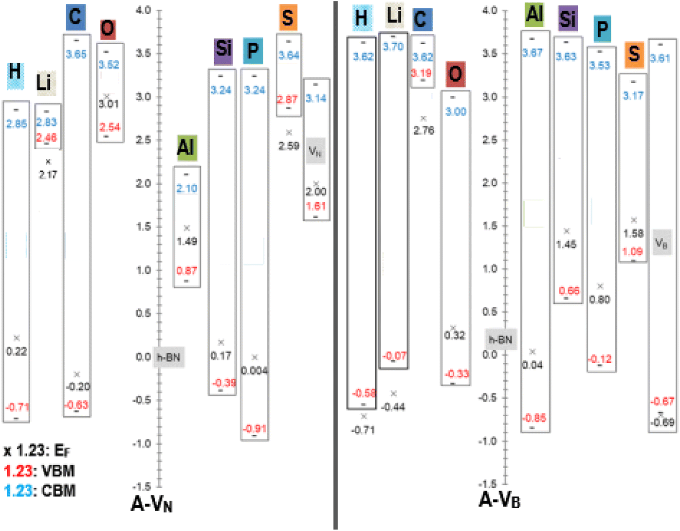 | ||
| Fig. 5 Fermi energy levels EF, VBM, and CBM with respect to pristine h-BN (EF = −3.686 eV), for A-VN and A-VB (A = H, Li, C, O, Al, Si, P, and S). All energy units are in (eV). | ||
The raw energy values for each product can be calculated from information given in Fig. 5 by adding (−3.686) to the values displayed in the figure. As an example, raw energy values for O-VN: EF is −3.686 + 3.01 = −0.676 eV; VBM is −3.686 + 2.54 = −1.146 eV; CBM is −3.686 + 3.52 = −0.166 eV. The band gap values also correspond with the values tabulated in Table 2.
An example of the usefulness of Fig. 5 may arise in investigations of using material with adhered A-VN and/or A-VB layers as one electrode of a two-electrode setup in contact with a redox electrolyte for catalytic, or photo electrochemical applications. Here, the position of the EF, VBM and CBM energy levels (of liquid and electrodes) and ERedox of the composite system (solid electrodes + liquid) will dictate the outcome as it will depend on shifts and differences in magnitudes of the energy levels as redox reactions occur and/or the composite material is illuminated by some light source. The alkali atom doping of 5 × 5 BN sheet, studied by Denis et al.,19 found Eg values of 1.78/4.45 eV for Li dopant and 4.45/1.0 eV for H dopant where the 2 values represent spin ↑/spin↓ gap.
The full spin polarised DOS (SDOS) plots for pristine VN, VB, and all the A-VN, A-VB products, from the spin polarised calculations, are presented in Fig. S1 to S10 of the ESI.† All SDOS plots are with respect to the EF level of the material i.e., the zero point is equal to EF (eV). The full plots indicate the VBM, CBM levels, s- and p- orbital contribution from the B, N, and adatom. To enhance the visibility of the adatom contribution to the full SDOS spectrum, the DOS magnitudes of the adatom have been multiplied by a factor of ×10 to ×50 and are shown in the graph's legend. Included are magnification plots of the EF region specifically displaying any s, p, px, py, and pz orbital contribution from the adatom.
Energy band levels and spin states, taken from the SDOS plots, for the adatom with orbital contributions, in the EF region are summarised in Table 4. Any orbital (i.e., s, px, py, or pz) contributions from the adatom are given in blue with spin states indicated by the red arrows. Included in the table are any difference (or widths) in the spin polarisation (ΔEs). Analysis of all DOS plots reveals that all of the adatoms, except for Li in Li-VB, have orbital contributions near the vicinity of the EF level.
| A | Ea | ΔEsb | |
|---|---|---|---|
| a E (eV) is given with respect to the EF levels of A-VN or A-VB (EF is the zero point), i.e., unmodified energy level = E (from this table) + EF (for A-VN or A-VB deduced from Fig. 5).b Difference (or width) in the spin polarisation ΔEs (eV c–e have been displayed correctly in Table 4.). The bold indicates spin polarization across the EF level.c Not in VBM/EF/CBM region.d No adatom contribution in the vicinity of EF. | |||
| (a) 1st row atoms A = H, Li, C, and O | |||
| H | VN | −0.92↑↓ s | — |
| VB | −1.39↑/+0.13↓ s | 1.52 | |
| Li | VN | −0.28↓/+0.32↑ s | 0.6 |
| VB | d | ||
| C | VN | −0.42↑/+0.43↓ pz | 0.85 |
| −1.84↑/−1.72↓ pzc | 0.12 | ||
| VB | −0.43↑/+0.47↓ pz | 0.90 | |
| O | VN | −0.46↓ py pz | — |
| +0.58↑/+0.54↓ pz | 0.04 | ||
| VB | −0.66↑/−0.92↓ py pz | 0.26 | |
| +0.66↓ py pz | |||
|
|||
| (b) 2nd row atoms A = Al, Si, P, and S | |||
| Al | VN | −0.61↑↓ px py pz | — |
| +0.63↑↓ px py | — | ||
| +0.99↑↓ pzc | — | ||
| VB | −2.18 px pyc | ||
| Si | VN | −0.59↑/+0.55↓ pz | 1.14 |
| −0.67↑/−0.55↓ px py | 0.12 | ||
| VB | −0.78↑/+0.80↓ pz | 1.58 | |
| P | VN | −1.10↑↓ pzc | — |
| −1.28↑↓ px pyc | — | ||
| +3.24 ↑↓ pz | — | ||
| VB | −0.92↑↓ s pz | — | |
| +2.78↑↓ px py | — | ||
| S | VN | −0.25↓/+0.27↑ p | 0.2 |
| VB | −0.47↑/+0.49↓ py | 0.96 | |
| +1.61↑/+1.71↓ px py | 1.0 | ||
Table 4 shows that half of the products have a spin polarization at the EF level of width between 0.5–1.58 eV. Energy levels further from EF with spin polarization have smaller widths between 0.1–0.12 eV. For the p block adatoms (C, O, Al, Si, P, and S) the main orbital contribution from the adsorbate near EF is from the pz orbitals with a spin polarization. Inspection of all the SDOS plots reveal a decrease in the density of states at the Fermi level results from a state crossing the Fermi level and a decrease of that state. The O-VN and O-VB products are different in that they have no spin polarization at the EF region and also non-zero magnetic moments.
The SDOS plots indicate that the 2p and 3p valency orbitals have a wide distribution in the valence band up to the Fermi energy level. It will be interesting to derive the average energy for the orbital center (εp) of the adatom 2p or 3p valency orbitals. The orbital center of the adatom is calculated from the projected density of states of a given adatom in an energy interval that is basically the widths of the valence band up to EF. The idea is from the d-band center (εd) that is widely used to interpret and predict interaction strengths for many different adsorbates and metals for metal surface activity such as catalytic activity. It is a useful measure of the position of the d-states in interactions that involve atoms with d-orbitals.32,33 The orbital centers for the adsorbates, in the A-VN and A-VB products, were calculated from a total energy width up to the EF level ranging from −9.5 eV to −13.5 eV, by the dosanalyze.pl Perl routine from the VST tools packages.28 Fig. 6 displays the calculated orbital centers of the adatoms in the A-VN and A-VB products with details of the valence bandwidth and standard deviation errors included in Fig. S11 and S12 of the ESI.†
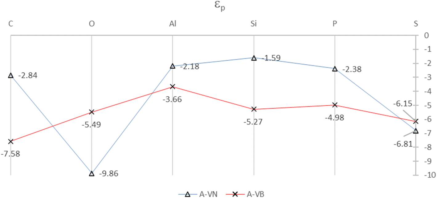 | ||
| Fig. 6 Orbital centers, εp, of 2p and 3p orbital bands for the adatoms for the A-VN and A-VB products. The full colour lines are drawn as a guide to the eye. All units are in eV. | ||
A general trend in the average energy, εp of the p orbital bands from Fig. 6 is that with the A-VN products, except for O-VN and S-VN, the availability (occupation) of p electrons for interaction are mainly from localised states near EF. This trend follows the general rule that electrons at the Fermi level are the most energetically available electrons for chemical reaction. In contrast the A-VB products, O-VN and S-VN, the interaction of the adsorbate atoms and the BN surface involves the availability (occupation) of adsorbate p electrons from states in the entire p-band. The trend of the orbital centers is similar to the trend in interaction strength of adsorption for both A-VN and A-VB, with slight variation for the C and O adsorbates, suggesting some correlation between interaction strength and the p-center.
3.3 Carbon monoxide (CO) reaction with A-VN and A-VB surfaces
An exploration of the chemical reactivity of the surfaces, from Section 3.2, with the simple CO diatomic molecule is made to ascertain the thermodynamic feasibility of the reaction. Adsorption of CO molecule on Al doped h-BN (notated as Al-BN), studied by Zhang et al.37 showed strong interaction with Al-BN, with a resulting Al–CO bond of 2.12 (Å) and Eb of −0.75 (eV) which are similar to calculated Al-(CO-VN) values of Table 5 below. Adsorption of CO molecule on Si doped BN nanotubes (termed BNNT) were theoretically studied by Wang and Zhang.38 The Si replaced a B or N atom (termed SiN-BNNT-CO and SiB-BNNT-CO) at two different configurations in the nanotube. The results for SiN-BNNT-CO had the CO molecule at 1.922 Å and 1.749 Å from the BNNT while for SiB-BNNT-CO the CO was 1.96 Å and 3.907 Å from the BNNT and reaction energies in the range −0.038 to −0.756 (eV). Tabtimsai et al.,39 theoretically investigated CO adsorption on C doped pristine and Stone–Wales defected single wall BNNT with various configurations of the doping. The calculations show the CO molecule at a range of 2.393 Å to 3.249 Å from the BNNT.| A | Eb (eV) | C–O (Å) | A–CO (Å) | rA + rC (Å) |
|---|---|---|---|---|
| a rA = adatom (A = H, Li, C, O, or Si) atomic radii and rC = carbon atom radius; Eb = reaction energy (eV).b CO bonds to site ➂ i.e., C–N bond; H bonds to a N atom from BN matrix.c CO bonds to site ➂ i.e., C–B bond; O-site distances, of the adatom, are unchanged and in-plane. | ||||
| (a) CO-(A-VN) | ||||
| Li | −1.1 | 1.15 | 2.1 | 2.3 |
| C | −0.1 | 1.19 | 1.5 | 1.5 |
| O | −1.1 | 1.19 | 1.7c | 1.6c |
| Al | −2.1 | 1.16 | 1.9 | 2.2 |
|
||||
| (b) CO-(A-VB) | ||||
| H | −4.1 | 1.21 | 1.5b | 1.5b |
| Li | −0.1 | 1.13 | 2.2 | 2.3 |
| Al | −0.1 | 1.13 | 2.2 | 2.2 |
| Si | −0.1 | 1.18 | 1.8 | 2.0 |
In a previous DFT investigation on molecular interactions with defected h-BN, by the current authors,31 it was also determined that it is thermodynamically feasible for the CO molecule to react with the pristine VN and VB surfaces. The DFT results indicated that the CO molecule bonded to the VB surface via the C atom and N sites of the surface in a vertical configuration. However, bonding of the CO molecule with the VN surface occurred by the O atom bonding with the B sites or the C and O atoms bonding with the B sites, depending on whether the CO molecular axis was vertically or horizontally aligned to the BN plane in the interaction.
In the present investigation the VN and VB surfaces have an adatom in the vacancy space and as such interaction of other molecular species will either chemically bond with the adatom, be physisorbed, or break up the adatom-surface configuration. The DFT results predict the three possibilities can occur with diatomic CO reacting with the adatom bonded to the BN surface. Table 5 lists results of the reaction energies (Eb), C–O lengths, and A–CO distances (A = H, Li, C, O, Al, Si, P, S) for successful adatom chemical bonding reactions. The overall product geometry for successful A–CO bonding is indicated in Fig. 7, and shown for the Al adatom product. The adatom (A) bonds to the carbon of the CO molecule with the (A–C–O) component perpendicular to the BN surface plane i.e., CO pillars. In contrast, the H-VB product has the H atom bonding to a N atom from the BN surface while the CO molecule bonds to the N atom of site ➂.
 | ||
Fig. 7 General product geometry of CO bonded to the adatom of the A-VN and A-VB surfaces.     and and  (shown is the Al adatom). (shown is the Al adatom). | ||
Structural energy minimisation of CO reacting with H-VN, S-VN, and P-VB could not reach convergence and with the CO molecule >3 Å from the surface resulting in physisorption process. CO interaction with P-VN results with P adatom displaced closer to the BN surface plane, but with CO approximately 5 Å from surface. The reaction of CO with Si-VN results in the Si adatom detaching from the BN surface. The CO reaction with C-VB and O-VB products have the CO molecular axis parallel with the surface and with the molecule >2.5 Å from the surface, suggesting a predominant physisorption process. The CO-(C-VN) distance is much shorter than distances listed for the CO interactions with BNNT studied by.39
An interesting outcome is from the reaction of CO with S-VN which results in S–C and O.
i.e., CO + S-VN ⇒ S–C + O + [VN surface].
Since the calculated S–C distance (1.89 Å) is not very different from the bond length derived by the atomic radii (1.81 Å) can claim a S–C bond is formed with the molecule stretched and with an activated O atom in an excited state. It may be possible to use the S–C product to form a carbon-sulphur polymer (CS), as theoretically hypothesised by Genin and Hoffmann30 by the extended Hückel method, or use the activated O atom for physiochemical interactions.
4. Summary/discussion
In summary, it's thermodynamic feasible to produce h-BN mono layers with single a vacancy defect (N or B) and have elemental atoms (A) from the 1st and 2nd row elements (A = H, Li, C, O, Al, Si, P, and S) react, with high negative binding/adsorption energies, and bond with the defected h-BN surface. The Bader charge differences from/to the adatom are of significant magnitude with significant chemical bonding of adatom-surface atom plus stability of the whole BN layer to warrant investigation of the A-VN and A-VB products for further chemical synthesis applications.The A-VN and A-VB material show a range of solid-state electronic properties, derived from spin polarised calculations and resulting DOS plot: total magnetic moments for the materials with significant contribution from the adatom; lowering of the energy band gap; adatom contribution to the Fermi energy level, EF; significant spin polarisation in the EF region, from adatom. These properties, arise from directional p-orbital (s-orbital for H and Li atom) interactions with the adatoms towards the surface. Calculation of p-band centers show the adsorbates from the A-VN products have most of their available p electrons from localised states near EF while the A-VB products have available p electrons energies further away from EF (>−3.5 eV). Predicted EF, VBM and CBM values may be of use in investigating systems containing the A-VN and A-VB monolayer material interacting with other solid or liquid surfaces, e.g.: A-VN/A-VB-metal surfaces; A-VN/A-VB-electrolyte-metal interaction, possible for catalytic, or photo electrochemical applications.
The DFT exploration on diatomic molecule reaction with the A-VN and A-VB products indicate chemical reactivity of CO with some of the products resulting in ‘pillars’ of CO attached to the adatom of the surfaces. Other predicted outcomes, from the CO reactions, include detachment of the adsorbed atom (e.g., Si), discrete A–C species (e.g., S–C) and excited O atom from the C–O molecule break up.
5. Conclusions
This comprehensive DFT-driven work has thoroughly investigated structural and electronic properties pertinent to the interaction of 1st and 2nd periodic-table elements, in addition to CO, with pristine and N/B defect mono-layer BN surfaces. Attachment of a CO molecule above a nitrogen vacant site dissociates the molecule in a reaction that occupies the vacant site with the carbon atom. Binding energies of the CO molecule noticeably varies with the adatom adsorbents for all considered BN structures. Analysis of electronic properties indicates that interaction of the adsorbate atoms with surface mainly involves occupation of adsorbate p electrons. The orbital centres for the adsorbates were calculated from a total energy width up to the Fermi level. Creation of the B and N surface defects and the subsequent atomic adsorption on the surface are all thermodynamically feasible processes. Findings here shall find direct applications in efforts that target the wide-scale utilization of BN-monolayers in optical and catalytic applications where the high surface area BN serves as supports and the decorated atoms represents the active sites in chemical sensing and reactions. We anticipate that an interesting extension of the current work is to compute other important properties' most notably IR spectra for the various configurations.Conflicts of interest
There are no conflicts to declare.Acknowledgements
NM is grateful to the Australian Government for providing financial support under Australian Postgraduate Awards (APA) via Murdoch University. The National Computational Infrastructure (NCI) in Canberra as well as Pawsey Supercomputing Centre in Perth, Australia has provided grants for the computational resources.References
- C. Tan, X. Cao, X.-J. Wu, Q. He, J. Yang, X. Zhang, J. Chen, W. Zhao, S. Han, G.-H. Nam, M. Sindoro and H. Zhang, Recent advances in ultrathin two-dimensional nanomaterials, Chem. Rev., 2017, 117, 6225–6331 CrossRef CAS PubMed.
- H. Zang, Ultrathin two-dimensional nanomaterials, ACS Nano, 2015, 9, 9451–9469 CrossRef PubMed.
- G. Siegel, C. V. Ciobanu, B. Narayanan, M. Snure and S. C. Badescu, Heterogeneous pyrolysis: a route for epitaxial growth of hBN atomic layers on copper using separate boron and nitrogen precursors, Nano Lett., 2017, 17, 2404–2413 CrossRef CAS PubMed.
- T. Vogl, G. Campbell, B. C. Buchler, Y. Lu and P. K. Lam, Fabrication and deterministic transfer of high-quality quantum emitters in hexagonal boron nitride, ACS Photonics, 2018, 5(6), 2305–2312 CrossRef CAS.
- Q. Weng, X. Wang, X. Wang, Y. Bando and D. Golberg, Functionalized hexagonal boron nitride nanomaterials: emerging properties and applications, Chem. Soc. Rev., 2016, 45, 3989–4012 RSC.
- L.-H. Li and Y. Chen, Atomically thin boron nitride: Unique properties and applications, Adv. Funct. Mater., 2016, 26, 2594–2608 CrossRef CAS.
- F. Späth, J. Steinhauer, F. Düll, U. Bauer, P. Bachmann, H.-P. Steinrück and C. Papp, Reaction of hydrogen and oxygen on h–BN, J. Phys. Chem. C, 2020, 124, 18141–18146, DOI:10.1021/acs.jpcc.0c05299.
- R. S. Singh, R. Y. Tay, W. L. Chow, S. H. Tsang, G. Mallick and E. H. Tong Teo, Band gap effects of hexagonal boron nitride using oxygen plasma, Appl. Phys. Lett., 2014, 104, 163101, DOI:10.1063/1.4872318.
- C. Ma, Y. Zhang, S. Yan and B. Li, Carbon-doped boron nitride nanosheets: A high-efficient electrocatalyst for ambient nitrogen reduction, Appl. Catal., B, 2022, 315, 121574 CrossRef CAS.
- X. Wang, Z. Cheng, G. Zhang, H. Yuan, H. Chen and X.-L. Wang, Spin-gapless semiconductors for future spintronics and electronics, Phys. Rep., 2020, 888, 1–57 CrossRef CAS.
- M. Legesse, S. N. Rashkeev, H. Saidaoui, F. El Mellouhi, S. Ahzi and F. H. Alharbi, Band gap tuning in aluminum doped two-dimensional hexagonal boron nitride, Mater. Chem. Phys., 2020, 250, 123176 CrossRef CAS.
- B. Lin, Y. Liu, Y. Li, F. Xu, Y. Zou and Y. Zhou, In situ growth of phosphorus-doped boron nitride on commercial alumina as a robust catalyst for direct dehydrogenation of ethylbenzene, Catal. Sci. Technol., 2022, 12, 962–968 RSC.
- S. Azevedo, J. R. Kaschny, C. M. C. de Castilho and F. de Brito Mota, Electronic structure of defects in a boron nitride monolayer, Eur. Phys. J. B, 2009, 67, 507–512 CrossRef CAS.
- A. S. Fedorov, Z. I. Popov, D. A. Fedorov, N. S. Eliseeva, M. V. Serjantova and A. A. Kuzubov, DFT investigation of the influence of ordered vacancies on elastic and magnetic properties of graphene and graphene-like SiC and BN structures, Phys. Status Solidi B, 2012, 249, 2549–2552 CrossRef CAS.
- B. Huang and H. Lee, Defect and impurity properties of hexagonal boron nitrides: A first-principles calculation, Phys. Rev. B: Condens. Matter Mater. Phys., 2012, 86, 245406 CrossRef.
- M. Abdi, J.-P. Chou, A. Gali and M. B. Plenio, Color centers in hexagonal boron nitride monolayers: a group theory and Ab initio analysis, ACS Photonics, 2018, 5, 1967–1976 CrossRef CAS.
- L.-S. Zhao, C.-P. Chen, L.-L. Liu, H.-X. Yu, Y. Chen and X.-C. Wang, Magnetism and piezoelectricity of hexagonal boron nitride with triangular vacancy, Chin. Phys. B, 2018, 27, 016301 CrossRef.
- Y. Pan and Z. Yang, Electronic structures and spin gapless semiconductors in BN nanoribbons with vacancies, Phys. Rev. B, 2020, 82, 195308 CrossRef.
- P. A. Denis, S. Ullahb and F. Iribarne, Reduction chemistry of hexagonal boron nitride sheets and graphene: a comparative study on the effect of alkali atom doping on their chemical reactivity, New J. Chem., 2020, 44, 5725–5730, 10.1039/D0NJ00414F.
- VASP – from Computational Materials Physics, Faculty of Physics, Universität Wien, Sensengasse 8/12, A-1090 Wien, Austria Search PubMed.
- G. Kresse and J. Furthmuller, Efficient iterative schemes for ab initio total-energy calculations using a plane-wave basis set, Phys. Rev. B: Condens. Matter Mater. Phys., 1996, 54, 11169–11186 CrossRef CAS PubMed.
- J. Paier, M. Marsman, K. Hummer, G. Kresse, I. C. Gerber and J. G. Ángyán, Screened hybrid density functionals applied to solids, J. Chem. Phys., 2006, 124, 154709 CrossRef CAS PubMed.
- P. E. Blochl, Projector augmented-wave method, Phys. Rev. B: Condens. Matter Mater. Phys., 1994, 50, 17953–17979 CrossRef PubMed.
- G. Kresse and D. Joubert, From ultrasoft pseudopotentials to the projector augmented wave method, Phys. Rev. B: Condens. Matter Mater. Phys., 1999, 59, 1758–1775 CrossRef CAS.
- M. Ernzerhof and G. E. Scuseria, Assessment of the Perdew−Burke−Ernzerhof exchange-correlation functional, J. Chem. Phys., 1999, 110, 5029–5036 CrossRef CAS.
- H. J. Monkhorst and J. D. Pack, Special points for Brillouin-zone integrations, Phys. Rev. B: Solid State, 1976, 13, 5188 CrossRef.
- S. Grimme, Semiempirical gga-type density functional constructed with a long-range dispersion correction, J. Comput. Chem., 2006, 27, 1787–1799 CrossRef CAS PubMed.
- VST Tools by the Henkelman group, University of Texas at Austin, USA Search PubMed.
- K. Momma and F. Izumi, VESTA 3 for three-dimensional visualization of crystal, volumetric and morphology data, J. Appl. Crystallogr., 2011, 44, 1272–1276 CrossRef CAS.
- T. Genin and R. Hoffmann, Polythiene, a novel hypothetical Carbon-Sulfur polymer, J. Am. Chem. Soc., 1995, 117(49), 12328–12335 CrossRef.
- N. Mondinos, M. Altarawneh, A. Amri, W. Y. H. Liew, G. E. Poinern and Z.-T. Jiang, Molecular interaction with defected h-BN, Comput. Theor. Chem., 2022, 1217, 113911 CrossRef CAS.
- M. Mavrikakis, B. Hammer and J. K. Norskov, Effect of strain on the reactivity of metal surfaces, Phys. Rev. Lett., 1998, 81, 2819 CrossRef.
- J. R. Kitchin, J. K. Norskov, M. A. Barteau and J. G. Chen, Modification of the surface electronic and chemical properties of Pt (111) by subsurface 3d transition metals, J. Chem. Phys., 2004, 120, 10240 CrossRef CAS PubMed.
- P. A. Denis and F. Iribane, Comparative study of the chemical reactivity of graphene and boron nitride sheets, Comput. Theor. Chem., 2019, 1164, 112538, DOI:10.1016/J.COMPTC.2019.112538.
- E. G. Anota, A. Escobedo-Morales, M. S. Villanueva, O. Vazquez-Cuchillo and E. R. Rosas, On the influence of point defects on the structural and electronic properties of graphene-like sheets: a molecular simulation study, J. Mol. Model., 2013, 19, 839–846 CrossRef CAS PubMed.
- E. C. Anota, 2D boron nitride incorporating homonuclear boron bonds: stabilized in neutral, anionic and cationic charge, SN Appl. Sci., 2022, 11, 295 CrossRef.
- Y.-H. Zhang, K.-G. Zhou, X.-C. Gou, K.-F. Xie, H.-L. Zhang and Y. Peng, Effects of dopant and defect on the adsorption of carbon monoxide on graphitic boron nitride sheet: A first-principles study, Chem. Phys. Lett., 2010, 484, 266–270 CrossRef CAS.
- R. Wang and D. Zhang, Theoretical study of the adsorption of carbon monoxide on pristine and silicon-doped boron nitride Nanotubes, Aust. J. Chem., 2008, 61, 941–945 CrossRef CAS.
- C. Tabtimsai, A. Nonsri, N. Gratoo, N. Massiri, P. Suvanvapee and B. Wanno, Carbon monoxide adsorption on carbon atom doped perfect and Stone–Wales defect single-walled boron nitride nanotubes: a DFT investigation, Monatsh. Chem., 2014, 145, 725–735 CrossRef CAS.
Footnote |
| † Electronic supplementary information (ESI) available: Implementation of VASP code; Spin polarized DOS plots (SDOS) – Fig. S1–S10; average energy of p-orbital centers, εp – Fig. S11 & S12. See DOI: https://doi.org/10.1039/d3ra05108k |
| This journal is © The Royal Society of Chemistry 2023 |