
 Open Access Article
 This Open Access Article is licensed under a Creative Commons Attribution-Non Commercial 3.0 Unported Licence
Optical absorption performance of CZTS/ZnO thin film solar cells comprising anti-reflecting coating of texturing configuration
Abdulkarem H. M. Almawgani a,
Ahmad Alzahrania,
Ali Hajjiah*b,
Ahmed Mehaneyc,
Hussein A. Elsayed*c and
Hassan Sayedc
a,
Ahmad Alzahrania,
Ali Hajjiah*b,
Ahmed Mehaneyc,
Hussein A. Elsayed*c and
Hassan Sayedc
aElectrical Engineering Department, College of Engineering, Najran University, Najran, Saudi Arabia. E-mail: ahalmawgani@nu.edu.sa; asalzahrani@nu.edu.sa
bElectrical Engineering Department, College of Engineering and Petroleum, Kuwait University, Kuwait. E-mail: ali.hajjiah@ku.edu.kw
cPhysics Department, Faculty of Science, Beni-Suef University, Beni-Suef, 62512, Egypt. E-mail: Ahmed011236@science.bsu.edu.eg; drhussien85sc@gmail.com; hsayed330@yahoo.com
First published on 27th October 2023
Abstract
This paper introduces a novel design of a thin-film solar cell based on CZTS and ZnO composite materials with the help of ITO as the front contact layer. This study primarily focuses on how the cells' optical absorbance at visible wavelengths can be improved. COMSOL Multiphysics is employed as a powerful tool for the investigation of the numerical simulation. The numerical findings showed that the optimum thicknesses of the ITO and ZnO are 80 and 350 nm, respectively. In this regard, with a normal incidence, a wide range of incoming light wavelengths from 450 nm to 800 nm might result in optical absorption of the examined cell of above 0.9. However, this value decreased significantly to reach less than 0.75 when the angle of incidence increased to 50°. To minimize this reduction, on the top surface of the cell, a texture-designed anti-reflective coating designed from a single period of well-known one-dimensional photonic crystals is deposited. The findings demonstrated that the cell's absorption at normal incidence could reach over 0.96 through the overall incident wavelengths. Therefore, CZTS/ZnO thin-film solar cells with an anti-reflecting coating of texturing configuration showed enormous potential for manufacturing effective solar cells.
1. Introduction
In recent decades, economically advantageous methods of providing clean and carbon-neutral energy are envisioned to include the use of solar systems that are more widely available.1 Nonetheless, improving solar cell efficiency and making affordable photovoltaic panels seem to be of utmost importance.1,2 Although the c-Si-based technique provides a greater efficiency value of 26.6%, it has several weaknesses, the most notable of which is the high manufacturing cost owing to its processing stages, including purification and crystallization.2,3 Organic/inorganic, perovskite and dye-sensitized designs continue to be the basis for cost-effective solutions, which suffer from low conversion efficiency and dependability.3–5 In contrast, thin-film chalcogenide CuInxGa(1−x)Se2 (CGIS) solar cells are favorable because of their high stability and excellent efficiency of 22%.5–7 However, the use of hazardous or rare metals, such as gallium, germanium, indium, and cadmium in CGIS-based solar cells might make it difficult to achieve high efficiency/cost ratios. Accordingly, kesterite Cu2ZnSnS4 (CZTS) materials have the potential to be used for solar cell improvement because they are affordable, non-toxic, and exhibit unique optical features.8–10A semiconductor compound named CZTS is fabricated from elements, such as copper, tin, zinc, and sulfur, all of which are currently available and, they are not environmentally hazardous within the utilized levels compared to In and Ga in CIGS.11 Quaternary compounds, such as CZTS and Cu2ZnSnSe4 (CZTSe), are among the most promising ‘next generation’ photovoltaic materials, which received a lot of attention owing to their direct band gap energy between 1.4 and 1.6 eV, which is near the ideal band gap. In addition, its high absorption coefficient (>104 cm−1) and theoretically limited power conversion efficiency of 32.2% make it appropriate for optoelectronic uses.12,13 Despite being a relatively new material with a direct optical tunable bandgap of 1.52 eV,14 CZTS is a significant chalcogenide p-type semiconducting material that exists naturally. Meanwhile, CZTS as an absorbing material provides significant contributions through the next-generation solar cells.15 Therefore, the inclusion of CZTS through solar cells technology may be effective towards high efficiency and low cost solar cells.
By using thin-film technology, solar cell development is progressively advancing towards achieving affordable and efficient solar cells. To achieve this goal, the CZTS-based technology has received considerable interest owing to its efficiency, which is reported to be 9.5%, 12.6%, and 11.2% for standard CZTS structures, Se-alloying kesterite designs, and CZCTS solar cells using Cd-containing materials.16–18 The CZTS solar cells' power efficiency is significantly lower than that of CIGS thin film solar cells (22%).19,20 This low efficiency is attributed to the short lifetime of the minority carrier and the great resistance, which originates from the contact barrier due to the creation of MoS2 at the interface between the back contact of Mo and the absorbing layer of CZTS.21–23 The following sections examine the reflection spectrum from the top surface of the front contact (ITO), which is due to the big dielectric difference between ITO with refractive index (2.84–2.88) and the starting medium (air).24 Accordingly, this study aims to limit the reflectivity of the cell by using a simple and low-cost anti-reflecting coating (ARC). It is believed that new and artificial structures, i.e., photonic crystals (PCs), can fulfill this purpose.
PCs can be divided into three different categories, including one-dimensional (1D), two-dimensional (2D), and three-dimensional (3D) PCs. The structures of the artificially produced 1D-PCs are inhomogeneous with periodic variations in the refractive index in 1D and consistent in other dimensions.25–27 In general, PC structures have a superior ability to confine or tame the localization of the incident photons in a variety of ways according to the geometrical and optical characteristics of their constituent materials.28,29 1D-PCs are widespread in various applications owing to their simplicity of manufacture, low cost, and excellent control over the localization of electromagnetic waves. Therefore, they are utilized in waveguides,31 sensors,32 improved optical devices, and water desalination.30 1D-PCs may also be crucial for increasing solar cell efficiency.33–36
In this regard, PC structures are widely considered through the improvements in the optical properties of solar cells and their efficiencies. For this purpose, 1D, 2D and quasiperiodic PCs can significantly contribute to improving solar cell efficiencies.37–43 In this context, a 2D quasiperiodic PC structure is introduced by Hongjun et al. to improve the optical absorption of thin film silicon solar cells.37 The thin film silicon solar cell is sandwiched between an antireflecting coating (ARC) from a 2D PC design (cylindrical rods of Si3N4 in a hosting medium of SiO2) and a back reflector from quadrangular pyramids of ZnO on a substrate of Ag. Remarkably, the cell's optical absorption is improved to reach 0.92 through visible wavelengths. Moreover, the inclusion of a 1D PC design as a back mirror has led to a significant effect on the optical absorption of amorphous silicon solar cells.39 Particularly, the fabricated structure by Soman et al. provides a reflectivity of 0.97 through the wavelengths from 580 nm to 1200 nm.39 Furthermore, 2D PC designs are introduced by Peres et al. to improve light trapping through organic solar cells.41 Also, Elsayed et al. introduced simple designs of a 1D quadrant PC and a 1D binary PC to act as an ARC and back mirror, respectively for an amorphous silicon solar cell.43 The cell absorption increased to more than 0.9 in the wavelength domain from 350 nm to 640 nm. Significant decrements in cell absorption are investigated with the change in the angle of incidence. The above-mentioned designed and fabricated structures demonstrate a significant effect of PC designs in improving the optical absorption of different types of solar cells. However, the need for simple designs compared to complex structures of 2D and quasiperiodic PCs is essential to avoid the complexity through fabrication despite the excellent response to the optical properties of the solar cells. It is believed that the reduction of the cell absorption dissipation with the change in the angle of incidence could be crucial in improving cell efficiency. Notably, the angle of incidence changes along the day hours. The focus of this communication is to improve the absorption of CZTS/ZnO thin film solar cells in the vicinity of a simple design for the manufacturing procedure, as well as the reduction of optical absorption dissipation.
In this study, the focus is on the reduction of optical absorption dissipation versus the increase in the angle of incidence. In particular, the angle of incidence for the interacting electromagnetic waves changes along the day's hours. In this regard, our idea is mainly depending on the role of the optical path length of the incident radiation in improving the cell's absorption. Notably, the increase in the optical path of the incident electromagnetic waves inside the active area of the thin-film solar cell could lead to a significant increase in optical generation rate of the electron–hole pairs. As a result, the optical absorption of the cell is expected to increase. Meanwhile, the inclusion of an ARC from a simple design of the 1D-PC on the top surface of the solar cell could be effective. However, the cell's absorption values are drastically reduced when the incidence angle is changed from an ordinary scenario to an oblique one.43 Hence, the advantages of using 1D-PCs with a simple design as an ARC may be outweighed by those of using a texturing surface. Therefore, this study aims to overcome the cell's decreased absorbance at oblique incidence by modifying the morphology of the upper surface of the cell via texturing the surface in a pyramid shape. Notably, the texturing of the upper surface in a pyramid shape grants the reflected photons many opportunities to be absorbed inside the cell's active area. Thus, this strategy may boost the absorbance likelihood.
2. Modeling and simulation
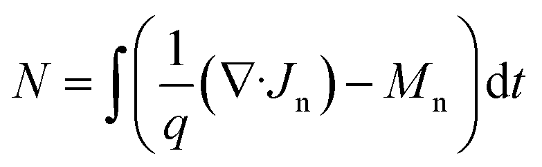
In this section, the structure and boundary conditions of CZTS/ZnO thin-film solar cells with various ARC shapes are illustrated. By using the COMSOL multiphysics modeling process, which utilizes the finite element method (FEM), 1D-PCs are explored using the transfer matrix method (TMM). Here, wave optics and semiconductor modules, as shown in eqn (1), produce the absorption properties in the presence of ARC for CZTS/ZnO solar cells. Finally, by resolving the continuity and Poisson equations, electron–hole pair creation rates that are close to these modules can be studied.44| A(λ) = 1 − T(λ)−R(λ) | (1) |
Since T(λ) represents the transmittance of the structure, and R(λ) denotes the reflectance of the structure. The electrostatic potential (Ψ), electron (N), and hole (P) concentrations in (cm−3), all of which can be calculated by solving continuity equations (eqn (3) and (4)) and Poisson (eqn (2))45 as follows:
| ∇·(εs∇Ψ) = −χ | (2) |
 | (3) |
 | (4) |
| χ = q(N − P + NA − ND) | (5) |
| Mn = recombinatonelectron − generationelectron | (6) |
| Mh = recombinatonhole − generationhole | (7) |
Thus, the heterojunction between the n-type ZnO buffer and the p-type CZTS absorber, as shown in Fig. 1, is considered the active area of the cell.
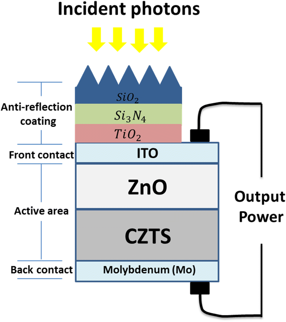 | ||
| Fig. 1 The thin film structure of the CZTS/ZnO solar cell with an ARC and two electrodes. The ARC is created using 1D-ternary PCs with the texturing of its upper surface. | ||
Fig. 1 depicts the usual composition of CZTS thin-film solar cells, which is comparable to that of CIGS devices. The investigated design is considered to be a chalcogenide thin film of P–N heterojunction. The heterojunction is produced at the p-type CZTS absorber (dCZTS) and n-type ZnO buffer layer (dZnO) interfaces. Moreover, the front finger contacts can be designed at the top of the solar cell using an Indian tin oxide (ITO) film because it acts as a good transparent conductive oxide (TCO). The back-contact electrode of CZTS-based solar systems is made of molybdenum (Mo). This is because the contact resistance of CZTS-based photovoltaic devices is improved after their stability at the processing temperature. Moreover, Molybdenum (Mo), which resembles silver and has the sixth-highest melting point of all elements, has a silvery appearance and exhibits a resistivity of over 5 × 10⁻⁵ (Ω cm).46
Hence, modeling a thin film solar cell structure (ZnO/CZTS) using COMSOL Multiphysics, the specific parameters, boundary conditions, and variables considered can vary depending on the specific goals and assumptions of the simulation. However, here is a general overview of the typical parameters and considerations:
Structure parameters
(1) ZnO layer: thickness, refractive index, absorption coefficient.
(2) CZTS absorber layer: thickness, bandgap, absorption coefficient, carrier mobility, and lifetime.
(3) Back contact and front contact: conductivity, thickness, and work function.
(4) Substrate: refractive index, thickness.
Optical properties
(1) Material dispersion models: depending on the available data and accuracy requirements, we can choose from various dispersion models such as Sellmeier, Cauchy, or Drude–Lorentz.
(2) Absorption models: the absorption coefficient can be determined experimentally or calculated using theoretical models such as the Tauc–Lorentz model or the Kubelka–Munk theory.
Carrier transport
(1) Carrier continuity equations: consideration of the drift-diffusion equations for electrons and holes, accounting for generation, recombination, and transport.
(2) Carrier mobility and lifetime: parameters that describe the mobility and lifetime of charge carriers in the CZTS absorber layer.
Boundary conditions
(1) Incident light: consider the angle of incidence, polarization, and spectral distribution of the incoming light.
(2) Contacts: appropriate boundary conditions, such as ohmic contacts or Schottky contacts, at the back and front interfaces.
(3) Insulating layers: boundary conditions to account for any insulating layers, if present.
Variables and outputs
(1) Electric potential: calculation of the electric potential distribution within the structure.
(2) Electric field: evaluation of the electric field distribution.
(3) Carrier concentrations: analysis of the distribution of electrons and holes.
(4) Photocurrent generation: calculation of the photocurrent generated within the CZTS absorber layer.
(5) Optical absorption: quantification of the absorption of incident photons within the structure.
It's important to note that the specific implementation and choices of parameters may vary based on the particular simulation setup and research objectives.
Now, to lower the dielectric contrast at the air and first layer of the cell interfaces, step-index structures are built, thereby resulting in a decrease in the reflectivity of the cell. In this regard, an ARC from a 1D ternary PC structure is configured as (ABC). Here, layer A is set as silicon dioxide (SiO2) with a thickness of (d1 = 54 nm), whereas layer B is designed from silicon nitride (Si3N4) with a thickness of d2 = 33 nm, and layer C is chosen as titanium dioxide (TiO2) with d3 = 82 nm. These specified materials are considered in the proposed ARC in this study to provide a gradual enhancement of the refractive index of the considered ARC. The indices of refraction for these materials are considered based on experimental studies.47–49 In other words, a single unit cell of a 1D ternary PCs could verify the step-index strategy to improve the cell's absorbance at a remarkable ratio, such that:
| nair < nSiO2 < nSi3N4 < nTiO2 < nITO | (8) |
Then, the dispersion relation of the cell layers is introduced, such as ITO, CZTS, and ZnO in the following figures. Fig. 2 depicts the refractive index and extinction coefficient of the ITO layer as a function of light wavelength. Here, it is observed that the extinction coefficient is lower than 0.1 at wavelengths larger than 350 nm, which means that the absorbance of this layer is very low. This response makes the ITO suitable for use in the proposed cells in this study. Notably, the limited absorption through this layer grants the incident photons to draft through the ZnO layer, which may, in turn, help improve the optical absorption of the cell. The refractive index equals 2.35 at 300 nm and, it decreases exponentially to 1.85 at 800 nm.24 These values of the refractive index are expected to create dielectric contrast at the ITO–air interface, which causes structural reflectance. In particular, the step-index strategy represents the mainstay towards achieving high absorption values for the cell. However, there is still a wide gap between the refractive index of the starting medium (air) and the ITO layer. Therefore, the dielectric contrast can be overcome by inserting an ARC with a grading index, as clarified in eqn (8).
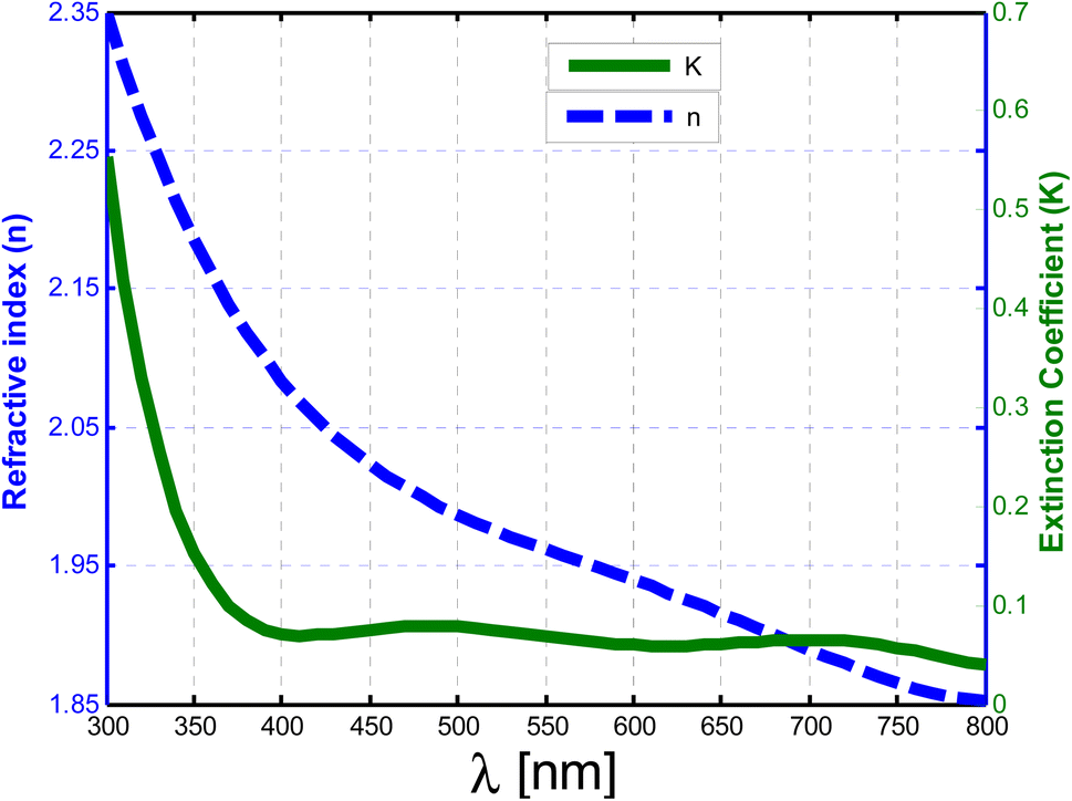 | ||
| Fig. 2 The refractive index (n) of the ITO vs. the incident wavelength, and extinction coefficient (k) of the ITO vs. the incident wavelength. | ||
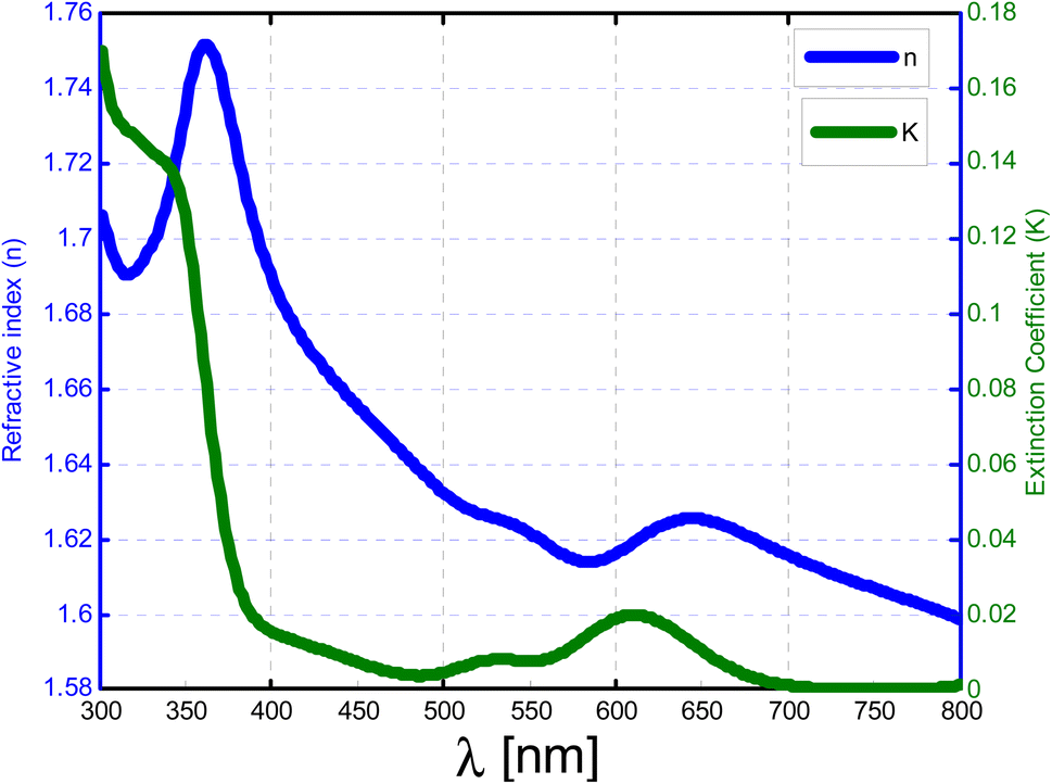
Fig. 3 shows the dispersion relation of the n-type semiconductor (ZnO), where the refractive index (n) equals 1.75 at 350 nm, and it decreases exponentially to 1.6 at 800 nm. Moreover, the extinction coefficient (k) equals 0.17 at 300 nm and decreases exponentially to 0.02 at 400 nm. Therefore, this layer has high absorbance at shorter wavelengths corresponding to its extinction coefficient.50,51 The bandgap of ZnO between 3.1 and 3.2 eV is obtained as in ref. 61, which means that the materials that are absorbed to the incident wavelength smaller than 400 nm and ZnO will be transparent to the wavelengths longer than 400 nm. The extinction coefficient decreases from 0.15 at 300 nm to 0.02 at 400 nm.62
 | ||
| Fig. 3 The refractive index (n) of the ZnO vs. the incident wavelength, and extinction coefficient (k) of the ZnO vs. the incident wavelength. | ||
The extinction coefficient of a material usually decreases with increasing wavelength in the optical range. In the case of ZnO, which has a bandgap around 400 nm, the absorption edge typically occurs at energies corresponding to shorter wavelengths (higher photon energies) than the bandgap energy. At wavelengths shorter than the absorption edge, ZnO exhibits strong absorption due to direct band-to-band transitions. The extinction coefficient, which is related to the absorption coefficient, quantifies the rate at which light is absorbed as it passes through a material. It is defined as the imaginary part of the refractive index and is typically wavelength-dependent. The extinction coefficient provides information about the degree of absorption of light within the material. In the case of ZnO, the extinction coefficient generally increases as the wavelength decreases (energies increase) approaching the absorption edge and the bandgap energy. This is because ZnO absorbs more strongly at shorter wavelengths due to direct bandgap absorption. However, once the wavelength exceeds the absorption edge and approaches longer wavelengths (lower energies), the absorption decreases, resulting in a decrease in the extinction coefficient. To summarize, the extinction coefficient of ZnO is expected to increase as the wavelength decreases (energies increase) approaching the absorption edge and the bandgap energy. However, beyond the absorption edge, the extinction coefficient decreases as the wavelength increases (energies decrease) in the optical range.
Now, Fig. 4 displays the dispersion relation of the p-type semiconductor (CZTS).52 The refractive index exhibits resonance peaks, as shown in the figure. In addition, the extinction coefficient approximately equals 1.2 at 300 nm and decreases to 0.27 at 800 nm. Therefore, this layer has high absorbance at shorter wavelengths. Thus, a high optical generation rate is expected in this region for high-energy photons (shorter wavelengths).
 | ||
| Fig. 4 The refractive index (n) of the CZTS vs. the incident wavelength, and extinction coefficient (k) of the CZTS versus the incident wavelength. | ||
3. Numerical results and discussion
A description of the optical absorption is presented for a CZTS thin-film solar cell. The findings are investigated in the vicinity of the optical properties of the solar cell's constituent materials and their thicknesses. The thicknesses of CZTS, ITO, ZnO, and Mo are specified as 350, 80, 350, and 100 nm, respectively. However, the optimization procedure for these values could potentially contribute to the improvement of optical absorption. Thus, the investigation has been carried out first in Subsection 3.1; the optimum thicknesses of the ITO and ZnO layers in the vicinity of the cell's optical absorption. Subsection 3.2 investigates the role of the incident angle as a real environmental parameter in the optical absorption of the considered solar cell. Then, Subsection 3.3 demonstrates the proposed method for improving cell absorption at different incidence angles. Finally, Subsection 3.4 demonstrates the cell's optical generation based on the ARC optimum design.3.1 Optimization of ZnO and ITO thicknesses
Fig. 5 describes the effect of the ITO thickness on the cell absorption at 350 nm, 250 nm, and 100 nm thicknesses of CZTS, ZnO, and Mo, respectively. The figure shows a significant contribution of ITO thickness to optical absorption at different wavelengths in normal incidence cases. As the ITO layer thickness varies between 80 nm and 120 nm, the cell's absorption is significantly influenced. Meanwhile, the cell absorption could receive values larger than 0.85 at an ITO layer thickness of 80 nm, specifically at wavelengths longer than 400 nm. By the way, at 730 nm, cell absorption achieves a maximum of 0.92. For wavelengths shorter than 400 nm, the absorption shows a slight decrease in its values due to the large values of the ITO extinction coefficient at these wavelengths, as previously investigated in Fig. 4. The optical absorbance of the cell suffers from a drop in values for thicknesses greater than 80 nm. Therefore, the choice of 80 nm as the thickness of the ITO layer is the optimum thickness for the considered thin-film solar cell design. For the smallest wavelengths from 300 to 400 nm, the extinction coefficient decreases exponentially from 0.6 to 0.05, as shown in Fig. 2, but in this region, the refractive index also has the highest value compared to other values or regions, indicating a high dielectric contrast between the air and the ITO layer. Therefore, the reflectivity of the structure in the range from 300 nm to 400 nm is higher than other values or regions, which adversely affects the absorbance of the structure.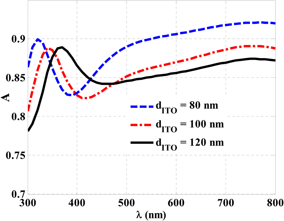 | ||
| Fig. 5 The optical absorption of CZTS/ZnO thin film solar cells at different thicknesses of the front contact layer (ITO) for normal incidence cases. | ||
Optimizing the thickness of the ITO layer, in a thin-film solar cell is typically related to achieve the balance between light absorption and electrical conductivity. The ITO layer is often positioned on top of the photoactive layer (such as amorphous silicon) to act as a transparent electrode, allowing incident light to reach the active layer while providing a pathway for extracting generated charge carriers. In some cases, optimizing the thickness of the ITO layer can enhance light absorption by ensuring that a significant portion of incident light passes through the layer and reaches the photoactive material. However, this optimization should be done carefully to avoid excessive absorption and optical losses within the ITO layer itself. Furthermore, the optimization of the thickness of the ITO layer is also important factor for achieving low resistivity and good charge carrier transport properties. An excessively thick ITO layer may lead to increased resistive losses, while a very thin layer may result in poor charge extraction efficiency. Hence, we notice that the large values of ITO extinction coefficients cause decrease in absorption. In general, larger values of the extinction coefficient indicate a higher absorption of light by the material. However, in the case of highly conducting materials like ITO, a large extinction coefficient can be associated with increased reflection rather than absorption. This is because highly conductive materials tend to exhibit strong reflection properties due to their high electrical conductivity, which hinders the penetration of light into the material. Thus, with increasing values of the ITO extinction coefficient, a larger portion of incident light is reflected rather than absorbed, leading to decreased absorption.
The minimum absorption value refers to the wavelength at which the material exhibits the lowest absorption. In the case of ITO films of different thicknesses, the minimum absorption value can vary due to interference effects caused by the layer thickness. When light interacts with a thin film, interference can occur between the light reflected at the top surface and the light reflected at the bottom surface of the film. The interference depends on the wavelength of the incident light, the refractive index of the film, and the film's thickness. As the film thickness changes, the interference pattern shifts, resulting in variations in the minimum absorption value at different wavelengths. For example, in the case of the 80 nm ITO film, the interference pattern may lead to destructive interference at a specific wavelength, resulting in a minimum absorption value. However, for the 120 nm ITO film, the thickness is different, and therefore, the interference pattern will be shifted, leading to a different wavelength for the minimum absorption value. The difference in the minimum absorption values between 120 nm and 80 nm ITO films can be attributed to interference effects and the thickness-dependent optical behavior of the films. The interference pattern and the resulting absorption depend on the film thickness, refractive index, and wavelength of the incident light. In general, thicker films exhibit more pronounced interference effects, leading to higher variations in absorption at different wavelengths. The 120 nm ITO film, being thicker than the 80 nm film, is more likely to exhibit stronger interference effects and, consequently, a higher minimum absorption value at a specific wavelength.
The relationship between the extinction coefficient and absorption is rooted in fundamental physics principles related to the interaction of light with matter. To better understand this relationship, it is essential to delve into the principles of optics and the behavior of electromagnetic waves. When light interacts with a material, it can be transmitted, reflected, or absorbed. The absorption of light occurs when the energy of the incident photons is transferred to the material's electrons, leading to an increase in their energy levels. This energy transfer can cause electronic excitations or promote electrons from the valence band to the conduction band, depending on the material's electronic structure.53,54
The absorption behavior of a material is quantified by the extinction coefficient (k), which is a measure of how strongly the material absorbs light at a specific wavelength. The extinction coefficient is related to the imaginary part of the complex refractive index (n + ik), where n represents the real part associated with the material's refractive properties. According to the Beer–Lambert Law, the absorption (A) of light in a material is directly proportional to the product of the extinction coefficient (k), the material thickness (d), and the incident intensity (Io). Mathematically, it can be expressed as A = 1 − T = 1 − e(−2kd),55 where T is the transmittance and e is the base of the natural logarithm. The extinction coefficient is related to the absorption coefficient (α) through the equation α = 4πk/λ, where λ is the wavelength of the incident light. The absorption coefficient represents the fraction of incident light absorbed per unit distance traveled in the material. The relationship between the extinction coefficient and absorption is thus evident. The higher the extinction coefficient, the stronger the absorption of light by the material, resulting in the decrement of the transmittance and an increase in absorption. Conversely, a lower extinction coefficient indicates a lower absorption, leading to higher transmittance. Therefore, the extinction coefficient serves as a crucial parameter for characterizing the absorption properties of a material.56–58
In Fig. 6, an optimization is carried out for the ZnO layer thickness at 350 nm, 80 nm, and 100 nm thicknesses of CZTS, ITO, and Mo, respectively. Here, ZnO is considered to be n-type in the proposed thin-film solar cell. Thus, optimization of its thickness is crucial for improving cell absorption. A heterojunction is created at the interface between the n-type (ZnO) buffer layer and p-type (CZTS) absorber. Therefore, the ZnO layer has two functions. The first function is to create the heterojunction at the interface with CZTS and the second function is to allow a large portion of the incident photons to transmit into the absorber layer (CZTS). Optimizing the thickness of ZnO is, therefore, a must to achieve the localization of incident photons at CZTS and high absorbance. Fig. 6 indicates that the optical absorption increases with increasing the ZnO thickness. An increase in the ZnO thickness may particularly reduce the transmittance of photons from the cell.59,60 Meanwhile, the increase in thickness from 150 nm to 250 nm and 350 nm improved absorption, particularly in the 400–500 nm wavelength range. This increase is attributed to the increase in the ZnO thickness, which causes an alteration in the optical path length of the incident photons. However, a further increase in the ZnO thickness to 450 nm results in a decrease in the absorption of the solar cell. Here, an increase in the ZnO thickness to some extent may lead to an increase in the recombination rate because of an exaggerated increase in the length of the optical path. Consequently, the choice of ZnO with a thickness of 350 nm represents the optimum value in this study.
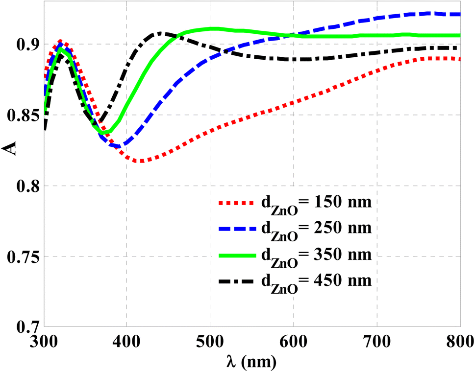 | ||
| Fig. 6 The optical absorption of CZTS/ZnO thin film solar cells at different thicknesses of the ZnO layer for a normal incidence case. | ||
When light passes through a thin film, interference phenomena can occur due to the multiple reflections at the film interfaces. These interference effects can lead to variations in the optical absorption depending on the film thickness and the wavelength of the incident light. Lower absorption at thicknesses of 250 nm and 400 nm. At these thicknesses, the ZnO layer may exhibit destructive interference with respect to the incident light at specific wavelengths. This interference can result in reducing the optical absorption, leading to lower absorption at these thicknesses. Also, higher absorption at a thickness of 350 nm can be investigated. At this thickness, the ZnO layer may exhibit constructive interference with respect to the incident light at certain wavelengths. This constructive interference enhances the optical absorption, resulting in higher absorption at this specific thickness.
The ZnO layer can contribute to light absorption within the cell, particularly at shorter wavelengths. By controlling the thickness of the ZnO layer, the absorption of photons within this layer can be optimized to increase the overall absorbance of the cell. Light trapping refers to the ability of the cell to confine and absorb light within the active layers, thereby increasing the path length of light and enhancing absorption. By optimizing the ZnO thickness, the cell can achieve better light trapping and thus enhance the overall absorbance. The thickness of the ZnO layer can also impact the generation of charge carriers (electrons and holes) within the cell. By controlling the thickness, it is possible to optimize the absorption of photons within the ZnO layer and facilitate efficient charge carrier generation at the interfaces. It's important to note that the optimal thickness for the ZnO layer can vary depending on the specific material properties, device architecture, and desired performance targets. Therefore, experimental characterization and optimization, as well as numerical simulations, are typically employed to determine the appropriate ZnO thickness for maximizing cell absorbance.
When light passes through an interface between two materials with different refractive indices, such as the ZnO layer and the surrounding medium (e.g., air or the absorber layer), a portion of the incident light is reflected back and a portion is refracted into the next medium. The amount of reflection and refraction depends on the refractive indices of the materials and the angle of incidence.63 With an increase in ZnO thickness, the number of interfaces the light encounters increases, leading to additional opportunities for reflection and refraction, which can reduce the overall transmittance of photons through the cell. Also, ZnO, like many materials, has an intrinsic absorption coefficient, which means it absorbs a certain amount of light as it passes through the material. As the thickness of the ZnO layer increases, the light has to traverse a greater volume of the material, resulting in a higher chance of absorption. This absorption can lead to a decrease in the transmittance of photons through the cell, as less light is transmitted through the thicker ZnO layer. It's important to note that the exact behavior of photon transmittance with increasing ZnO thickness can depend on various factors, including the refractive indices, incident angles, and specific design parameters of the solar cell structure.64,65
In the vicinity of Fig. 5 and 6, a comparison is performed between the reflectivity and absorption of the cell at the optimum thicknesses of ITO and ZnO at the normal incidence in Fig. 7. The solar cell absorption is almost greater than 0.83 for all incident electromagnetic waves. Moreover, its value can exceed 0.9, through a broad band of incident wavelengths in the range of 450–800 nm. On the other hand, the reflectivity is not exceedingly greater than 0.1 for most incident wavelengths. Therefore, the considered design may be of significant interest. However, it is believed that studying solar cell absorption at different incident angles could be more practical and realistic. Therefore, this role will be considered in the following subsection.
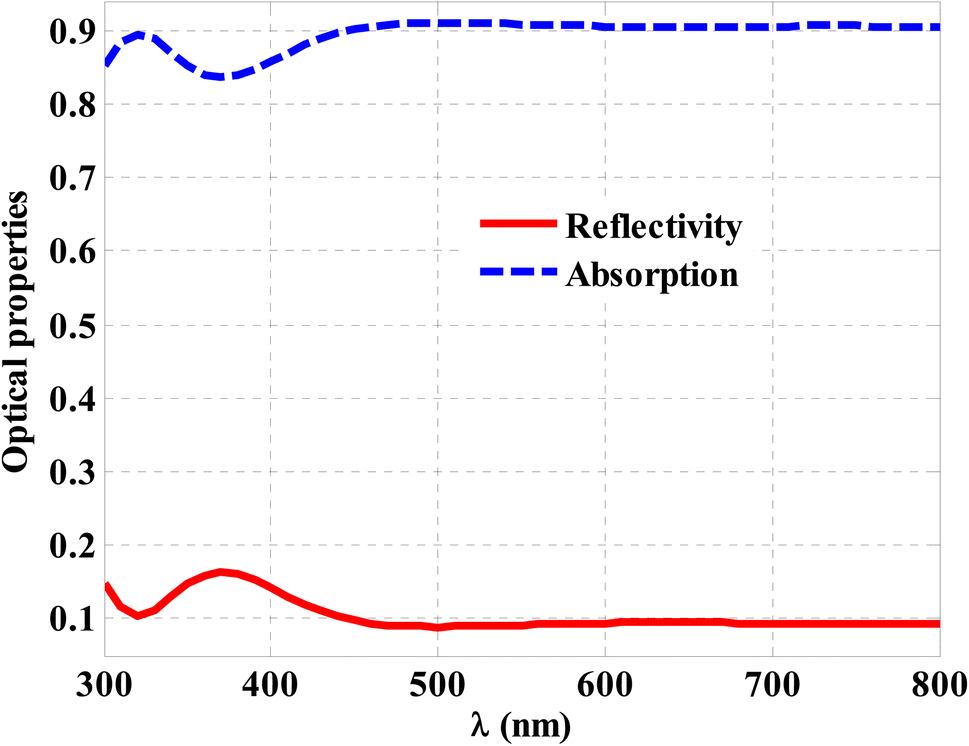 | ||
| Fig. 7 The optical properties of CZTS/ZnO thin film solar cells at the optimum thicknesses of ZnO and ITO for normal incidence cases. | ||
3.2 Dependency of cell absorption on the incident angle
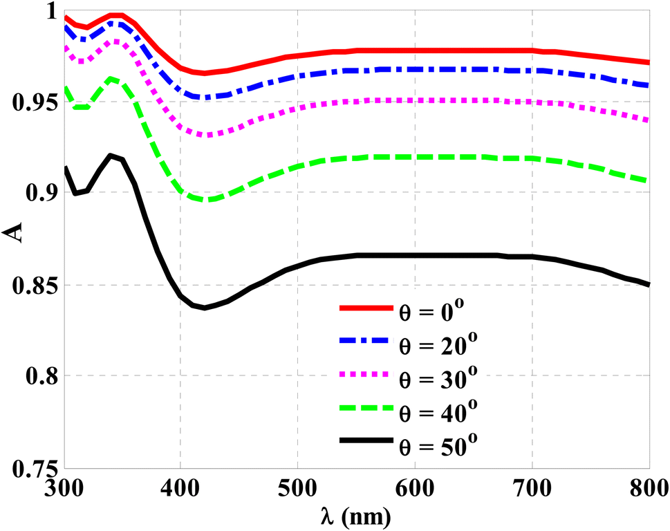
This section demonstrates the optical absorption response of the proposed designed thin-film solar cell at different incidence angles. In particular, the value of the incident angle changes significantly throughout the day; this could have a favorable impact on the cell's optical absorption and efficiency. In this context, Fig. 8 depicts the solar cell absorption at various incidence angles. The optical absorption values were significantly affected over the entire spectrum. The absorption values decreased by 2% when the incident angle increased from 0° to 10°. However, when the angle of incidence reached 30°, 40°, and 50°, the absorption values gradually decreased, as shown in the figure. This decrease could reach up to 14% as the incidence angle varies from 0° to 50°. This significant decrease in the absorption of the cell with variations in the incident angle is attributed to the modification of the incident photons' optical path length. Therefore, the following subsection aims to solve this issue by considering an ARC over the cell's top surface. Thus, the straightforward layout of a single 1D-PCs unit cell is appropriate for this design. | ||
| Fig. 8 The response of the optical absorption of CZTS/ZnO thin film solar cells under different angles of incidence. | ||
3.3 The ARC impact on the cell's absorption
This subsection introduces the proposed strategy for controlling the drop in the cell's optical absorbance as the incidence angle increases. The introduced strategy is based on the design of an ARC to reduce the decrease. Therefore, a step-index structure is designed to lower the dielectric contrast at the air and first layer of the cell interface by reducing the reflectivity of the cell. In this regard, a 1D-PC structure is presented to play this role because of the essential contribution of PCs in tuning the propagation of electromagnetic radiation. In the proposed CZTS/ZnO thin-film solar cell, a single period of 1D ternary PCs has been assumed to function as an ARC. Meanwhile, the ternary ARC consists of three layers with different indices of refraction and thicknesses, arranged as (ABC). Here, the arrangement of these layers is dependent on the gradual increase in the refractive index, as listed in Section 2.Based on this strategy, Fig. 9 demonstrates the function of ARC in improving the absorption of the solar cell at normal incidence. Here, the optical absorption increased by more than 6% at wavelengths ranging from 450 nm to 800 nm. The absorption values increased by up to 16% when the wavelengths were less than 450 nm. The addition of ARC on the top surface of the cell may have decreased its reflectivity, which might account for the cell's increased absorption. The solar cell response in the presence of the ARC is shown in Fig. 10 at various angles of incidence. As the angle of incidence increases, the absorption of the cell can receive some enhancements compared to the results shown in Fig. 8. However, the reduction in the absorption values can be enhanced by increasing the incidence angle. Thus, the SiO2 design with textured or pyramidal geometry is considered, as shown in Fig. 1.
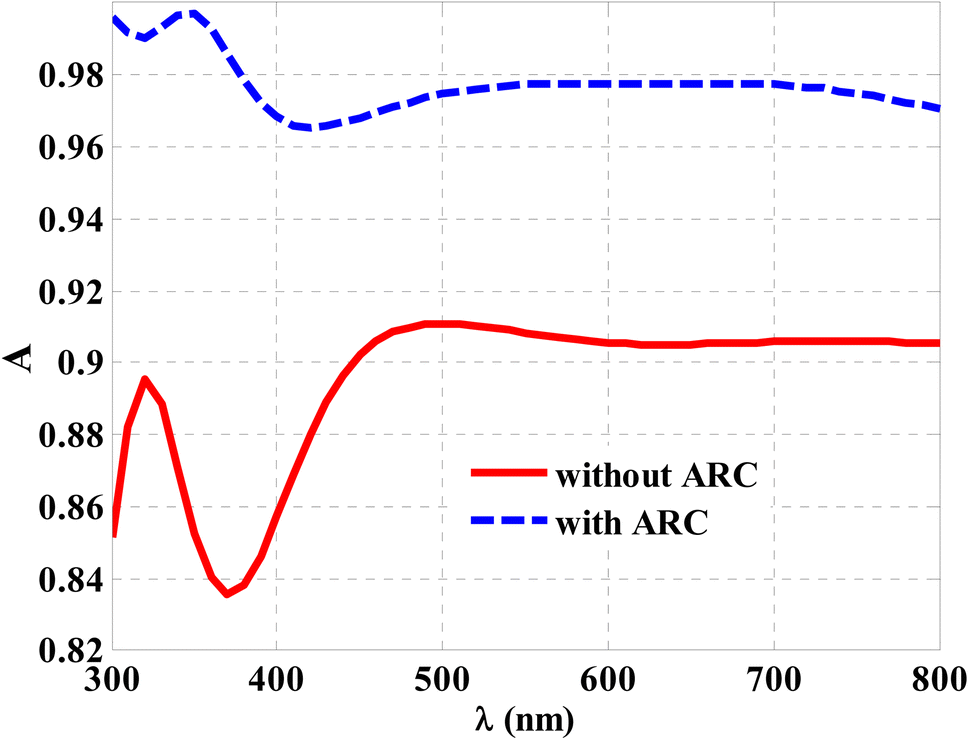 | ||
| Fig. 9 The optical absorption of CZTS/ZnO thin film solar cells with and without the ARC at normal incidence case. | ||
 | ||
| Fig. 10 The optical absorption of CZTS/ZnO thin film solar cells at different angles of incidence in the presence of the ARC. | ||
Fig. 11 describes a detailed comparison of the cell's absorption without the ARC, with the ARC of planar geometry, and with the ARC of textured geometry under various incidence angles. In this case, the texturing shape improves optical absorption as the angle of incidence increases because of reducing the cell reflectivity to some extent. In particular, the textured structure could provide reflected photons, providing a further opportunity to be absorbed into the cell. In other words, the texturing geometry could render the cell insensitive to the angle of incidence variations. A textured design with a height of 50 nm from SiO2 is deposited over the original layer, as indicated in Fig. 1.
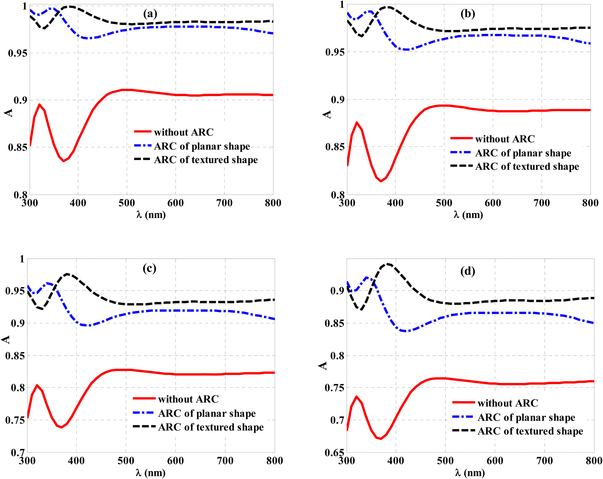 | ||
| Fig. 11 A detailed description of the cell's absorption without the ARC, with the ARC of planar shape and with the ARC of textured shape regarding the change of the angle of incidence for, (a) θ = 0°, (b) θ = 20°, (c) θ = 40° and (d) θ = 50°. | ||
In this regard, Fig. 11a describes the optical absorption of the designed cell at normal incidence without the ARC, with the ARC of planar geometry, and with the ARC of textured geometry. The figure shows that the dependence on the designed ARC of planar or textured shape can enrich the absorption of the cell by more than 6% and 7%, respectively. At an angle of incidence = 20°, the textured shape could help reduce the cell reflectivity compared to the planar shape. Notably, the minimum value for the optical absorption overall incident wavelengths has not been reduced by approximately 0.966, as shown in Fig. 11b. For a further increase in the incidence angle to 40° and 50°, the textured shape is almost still insensitive to the angle variations, recording a minimum value of 0.92 and 0.87°, as shown in Fig. 11c and d, respectively. In this context, it is believed that an ARC with a textured shape is a must to provide high optical absorption values, regardless of the change in the incident angle. In particular, the ARC with textured geometry could increase the cell's absorption between 1% and 5% by increasing the incident angle from 0° to 50°.
3.4 The optical generation of the cell
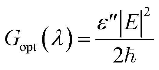
This section describes the optical generation of the proposed thin-film solar cells inside the ARC's optimal architecture. At various angles of incidence, the formation of electron–hole pairs is highlighted through the active area of the proposed thin-film solar cell in the presence of the textured ARC. The optical generation (Gopt(λ)) of electron–hole pairs at a single wavelength (λ) depends on two main parameters: the imaginary part of the permittivity (ε′′) and the intensity of the built-in electric field (E), as in the following equation:66
 | (9) |
The optical generation in a thin film solar cell ZnO/CZTS structure can depend on the refractive index and extinction coefficient of the materials involved. These parameters influence the optical properties of the materials; consequently, affect the absorption and generation of photons within the cell. Firstly, the refractive index determines how light interacts within the material. A higher refractive index leads to a larger difference in refractive indices at each interface, potentially increasing the amount of light trapped within the structure. This enhanced light trapping can result in a higher absorption of photons, leading to increased optical generation within the CZTS absorber layer. Also, the refractive index affects the optical path length of photons traveling through the material. A higher refractive index can lead to a longer path length, increasing the chances of photon absorption and generation of electron–hole pairs. Hence, the extinction coefficient quantifies the absorption of light by a material. A higher extinction coefficient indicates a higher absorption rate, meaning that more photons are absorbed within the material. In the CZTS absorber layer, a higher extinction coefficient can result in increased absorption of photons, leading to enhanced optical generation. In addition, the extinction coefficient is related to the penetration depth of photons into the material. A larger extinction coefficient corresponds to a shorter penetration depth, meaning that photons are absorbed closer to the surface. This can result in an efficient generation of electron–hole pairs near the interface between the CZTS absorber layer and the ZnO layer.
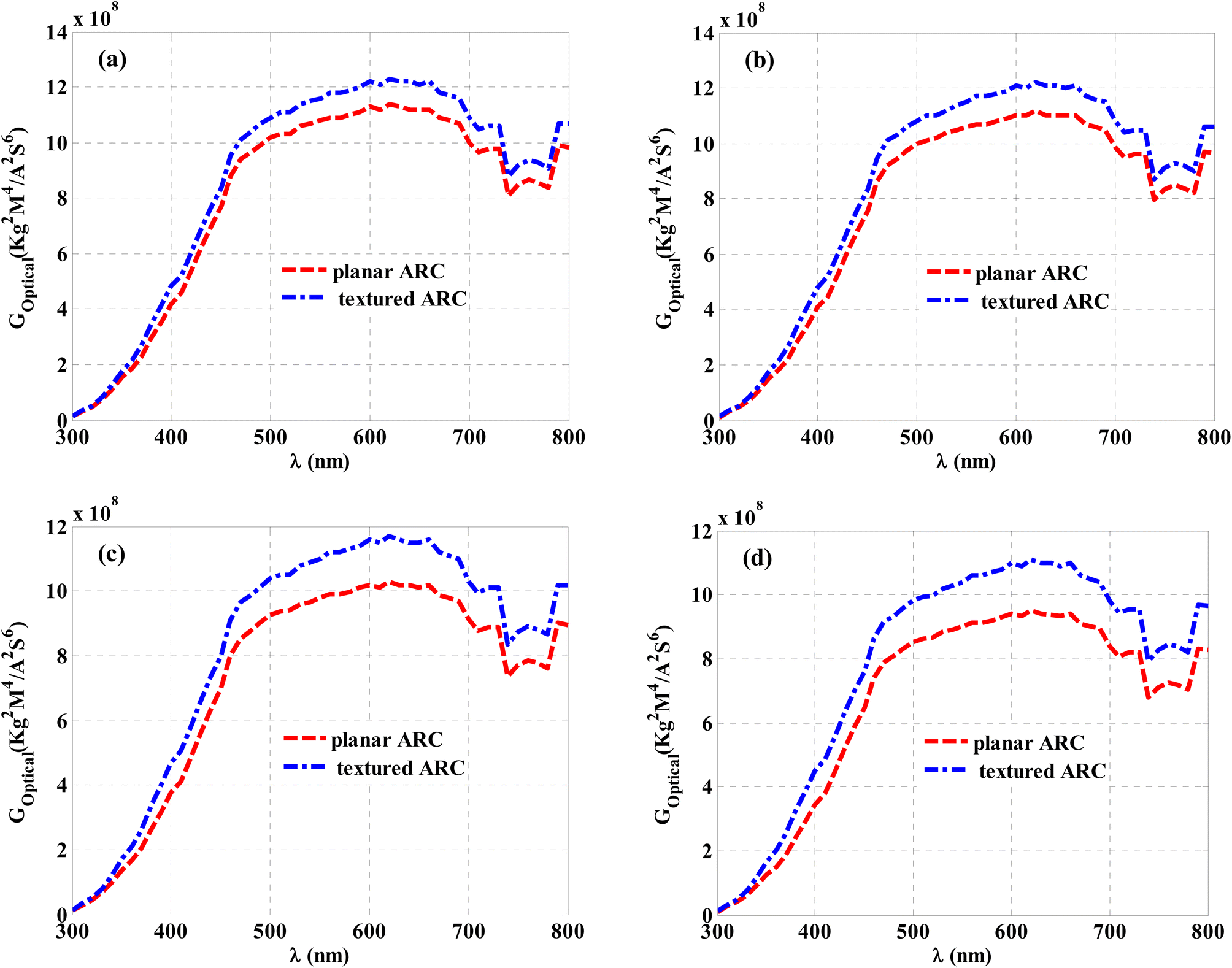
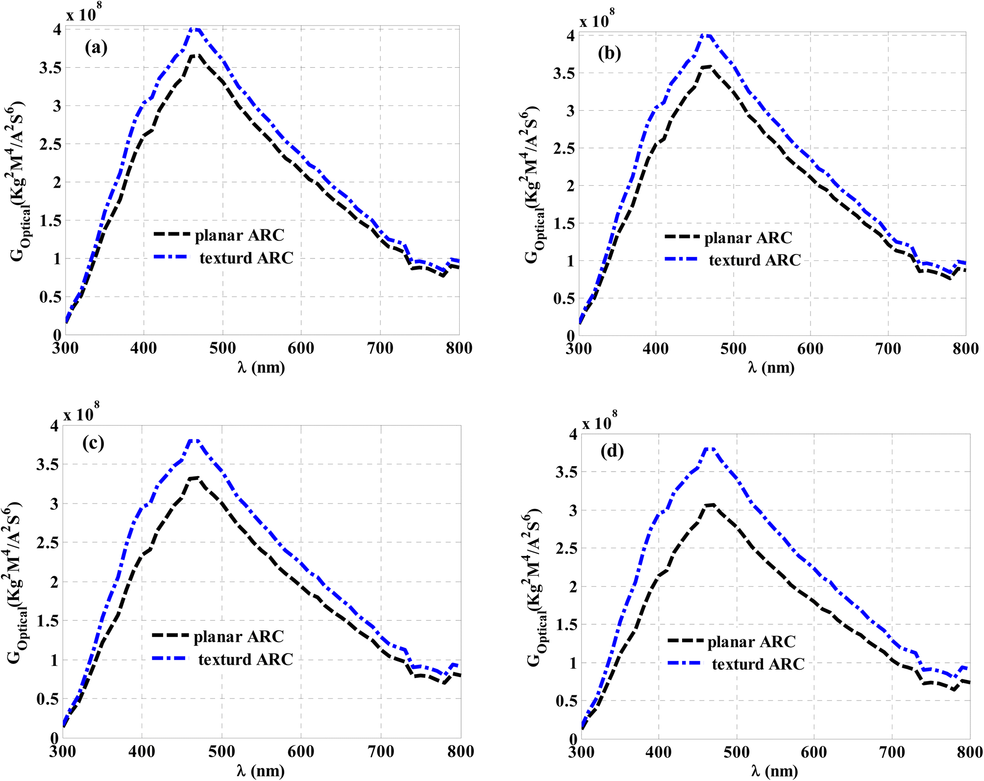
Fig. 12 and 13 present a detailed description of this role. This parameter is mainly dependent on the refractive index and extinction coefficient, as well as the n- and p-type of the considered solar cell.34 In this regard, Fig. 12 describes the optical generation through the ZnO layer, which represents the n-type of the proposed designed cell. In the normal incidence case, Fig. 12a shows an almost similar response of the optical generation at wavelengths less than 470 nm for both the textured and planar ARC. The contribution of the textured ARC to optical generation values is considerably important at wavelengths larger than 470 nm because of the role of the textured ARC in increasing the optical absorption of the cell. In particular, the optical bandgap of ZnO belongs to these wavelengths. Here, in Fig. 12a, we can divide the spectrum into two parts corresponding to the optical generation. First, for the incident wavelength less than 470 nm, the behaviors of planner and texturing are almost the same. In contrast, for the wavelengths greater than 470 nm, we have a remarkable enhancement for the texturing structure compared to the planner one. Hence, to explain the reasons of these behaviors, we must look at the dispersion relation of ZnO in Fig. 3. In Fig. 3, the extinction coefficient is high for incident wavelengths less than 470 nm, which leads to high absorption values and optical generation as well whatever the geometry of the upper surface. Then, for incident wavelengths greater than 470, there is a very low value of the extinction coefficient of the ZnO layer, which, in turn, leads to low absorbance values. Therefore, we are texturing the upper surface of the ARC structure to increase the optical path length of the incident photons, thus the absorption values could receive some significant increments at these wavelengths. Meanwhile, the optical generation in the ZnO layer could receive a remarkable improvement at wavelength greater than 470 nm by texturing the surface of the ARC. Therefore, photons of these wavelengths are absorbed to release more electrons. The optical generation showed a slight drop with an incident angle at a 20° angle of incidence. Moreover, the textured ARC contributed to increasing the optical generation values. When the incident angle increases to 40° °and 50°, the values of the optical generation suffer from some decrements, particularly in the absence of the textured ARC, as shown in Fig. 12c and d, respectively. These decreases are strongly related to the decrease in cell absorption and the increase in the incidence angle, as shown in Fig. 11c and d. Moreover, the optical generation depends on the intensity of the built-in electric field (E), which is created between the two edges of the depletion layer. Therefore, the generation of electron–hole pairs comes from the absorption of the incident photons within the junction between the ZnO (n-type) and CZTS (p-type). Then, by the effect of the built-in electric field, the electrons are moved to the n-type, which increases the generation rate in this region with the insensitive range of wavelength for this layer. Despite the resulting decreases in the cell's absorption and optical generation, as well as with the increase in the angle of incidence, the addition of the textured ARC could be promising.
 | ||
| Fig. 12 The optical generation through the ZnO layer with planar textured ARC regarding the change of the angle of incidence for, (a) θ = 0°, (b) θ = 20°, (c) θ = 40° and (d) θ = 50°. | ||
The high generation rate of positive charges (holes) for high-energy photons in the CZTS layer can be attributed to the electronic band structure and energy levels within the material. CZTS is a p-type semiconductor, which means it has an excess of holes (positive charge carriers) in its intrinsic state. This hole-rich nature is typically achieved through the presence of intrinsic defects or dopants that introduce acceptor levels in the energy band structure of CZTS. When high-energy photons (shorter wavelengths) are absorbed by CZTS, their energy is sufficient to promote electrons from the valence band to the conduction band, creating electron–hole pairs. However, due to the initial hole-rich nature of CZTS, the generated electrons are quickly captured by the available acceptor levels, leaving behind holes in the valence band. This preferential capture of electrons by the acceptor levels results in a higher generation rate of positive charges (holes) compared to negative charges (electrons) in the CZTS layer. Additionally, the energy band structure of CZTS plays a crucial role in the generation of holes. CZTS has a relatively narrow bandgap, typically around 1.0–1.5 eV, which in turn can absorb photons with higher energies (shorter wavelengths) compared to wider bandgap materials. The higher energy photons carry more energy, and when absorbed by CZTS, they can generate electron–hole pairs with higher kinetic energy. This higher kinetic energy can contribute to a higher generation rate of positive charges (holes) in the CZTS layer.
Fig. 13 elucidates the same role for the p-type of the proposed designed cell (CZTS layer). The figure shows a similar response for the ZnO layer, as shown in Fig. 12 for the ZnO layer. Here, the inclusion of a textured ARC on the top surface of the considered thin-film solar cell is crucial for providing high values of optical generation, especially when increasing the angle of incidence. At normal incidence, the spectrum receives its maximum values through wavelengths from 460 nm to 470 nm, as shown in Fig. 13a. The optical generation suffers from a slight decrease at an incidence angle of 20°, as shown in Fig. 13b. In contrast, the optical generation values are kept almost unchanged when the top surface is textured with ARC. When the angle of incidence is increased to 40° and 50°, the optical generation values suffer from some decrements, as shown in Fig. 13c and d. According to Fig. 11c and 11d, these reductions are a natural outcome of the decrease in cell absorption with an increase in the incidence angle. However, the use of the textured ARC may provide a suitable candidate to overcome the limitations of these decrements. The optical generation values in the presence of textured ARC showed a limited decrease compared to those in the absence of textured ARC. Therefore, it is believed that the inclusion of the textured ARC can maintain high absorption and high optical generation values, regardless of the angle of incidence.
 | ||
| Fig. 13 The optical generation through the CZTS layer with planer and textured ARC regarding the change of the angle of incidence for, (a) θ = 0°, (b) θ = 20°, (c) θ = 40° and (d) θ = 50°. | ||
The higher extinction coefficient of CZTS compared to ZnO across the entire wavelength range of 300–800 nm indicates that CZTS absorbs light more than ZnO. Therefore, one might expect the CZTS layer to exhibit higher optical generation. However, it is important to note that optical generation in a photovoltaic device depends not only on absorption but also on other factors such as the material's bandgap, carrier mobility, and carrier lifetime. These factors collectively determine the efficiency of converting absorbed light into charge carriers (electrons and holes) and their subsequent separation and collection.
In the case of CZTS, although it has a higher extinction coefficient and higher absorption, it also has a relatively wider bandgap compared to ZnO. The wider bandgap limits the absorption of lower-energy photons (longer wavelengths) that carry less energy. This can result in a reduced optical generation in the CZTS layer compared to the ZnO layer, which has a narrower bandgap and can absorb a broad range of photons. Additionally, the carrier mobility and lifetime in CZTS can also affect the overall optical generation efficiency. If the carrier mobility or lifetime in CZTS is lower than that in ZnO, it could hinder the efficient transport and collection of the generated charge carriers, leading to a lower overall optical generation despite the higher absorption. Therefore, while the extinction coefficient provides information about the absorption characteristics of a material, it is not the sole determinant of the optical generation efficiency in a photovoltaic device. The interplay of various factors such as bandgap, carrier mobility, and carrier lifetime, along with absorption, needs to be considered to understand the relative optical generation in different layers of a solar cell device.
4. Fabrication feasibility and experimental setup
In this section, a brief description of the reproducibility of the results and experimental feasibility of the 1D PC-designed structure is presented. It is worth mentioning that the experimental production of 1D PCs based on nano multilayer structures has been greatly verified for numerous applications over the past three decades.67–73 Also, the implementation of 1D PCs for solar cell applications has been studied in many experimental studies.74–77 Among these studies, the proposed structures have been investigated through IR and visible wavelengths. For fabricating these 1D PCs designs and the possibility of applying them in solar cells and other photonic applications, numerous techniques are used. For example, the spin coating,68 the electron-beam vacuum evaporator,67 the RF sputtering method,70 and the thermal evaporation.69 For the proposed 1D PC illustrated in Fig. 1, the fabrication of the thin 1D multilayer stacks is started by fabricating the anti-reflecting coating by depositing a smooth Si3N4 (33 nm) layer over the surface of a second dielectric material from TiO2 with the thickness value of 82 nm. This process can be accomplished by different techniques like RF sputtering and thermal evaporation technique.69,70 The upper surface of the Si3N4 material is covered with a texturing film of silicon dioxide (SiO2) with a thickness of 54 nm. SiO2 has outstanding properties, such as a low expansion coefficient, high thermal stability, and attractive mechanical chemical properties.78 The fabrication of a texturing film of SiO2 can be made using a facing target sputtering system.79 A previous study has also used 1D PCs to minimize the reflectance of the solar cell using the texturized surfaces.80 In this work, Laser interference lithography (LIL) is used to fabricate periodic models in photoresist (PR).81 The texturing morphology can be made to the silicon dioxide in many methods to obtain different shapes. Based on the required pattern, numerous materials can be deposited over the surface of the silicon to produce the starting stack. These materials can be deposited by spin coating with e-beam evaporation or by a Laurel WS-650S-6NPP-Lite Single wafer spin processor. Lastly, the produced pattern is bounded on the PR by using Lloyd's Mirrors.80 Then, it can be transferred to the underneath layer through reactive ion etching (RIE).The optical measurements of the proposed design in this study follow two septs. The first one is by varying the light wave incidence angle by using a rotating table to vary this angle. In addition, the absorption of the structure can be measured based on Fourier IR spectroscopy.82 Regarding the properties of Si3N4 and TiO2. Si3N4 has high-temperature strength and oxidation resistance, good wear resistance, and excellent thermal shock resistance.83 TiO2 is an abundant and inexpensive material, and it has other novel properties, including nontoxic, high chemical stability, and high dielectric constant, and it is widely used in the field of photonics.84
5. Discussions
Finally, in this section, we have introduced a brief comparison with some of the previously published works to highlight the novelty of the proposed design over its counterparts. In fact, the key novelty of our work lies in the improving of the proposed CZTS/ZnO thin-film solar cells' absorption regarding the angle of incidence. Meanwhile, incorporating the ARC of texturing configuration exhibits a significant contribution for the cell's absorption against the increase in the angle of incidence. The ARC enables the cell's absorption at normal incidence to surpass 0.96 across the entire range of incident wavelengths. However, the cell could suffer from a distinct reduction in its absorption values with the increase in the angle of incidence. In this regard, the texturing of the top surface of the designed ARC leads to keep over than 0.85 of the cell absorption at angle of incidence ≤ 50°. In contrast, adding ARC could reduce the reflectivity of the solar cell, as the rectangular PC profile reduces the reflectivity in the visible spectrum to 15.9%,85 while adding a circular PC profile reduces the reflectivity to 17.13%.85 Also, the triangular PC profile reduces the reflectivity in the visible spectrum to 10.6%.86 Moreover, adding a 1D triangular PC reduces the reflectivity to 7.01%.87 However, this study achieved a reflectivity of 4% for the visible incident photons, which is considered the best reflectivity compared to these previous works. In particular, the designed ARC provides the simplicity during the manufacturing procedure compared to its counterparts,37–43,85–87 as being composed of a single unit cell of the 1D PC besides its ability to achieve a minimum reflectivity of 0.04.6. Conclusion
This study investigates the possibility of reducing the absorption losses of thin-film solar cells based on 1D PCs. In particular, the absorption of the cell may suffer from a significant decrease in its values with the increase in the angle of incidence. Our solar cell was designed from two composite materials, including CZTS and ZnO, and considers ITO as a front contact layer. Our numerical findings demonstrated that the cell's absorption is significantly decreasing with the angle of incidence. Meanwhile, an ARC is designed from a single period of a 1D PC to reduce the dissipations in the absorption values with the increase in the angle of incidence. Moreover, these optical dissipations in the cell at oblique light incidence were overcome by modifying the morphology of the upper surface of the cell via texturing the surface in a pyramid shape. Physically, the pyramid shape can provide more opportunities for photons to be absorbed inside the cell's active area. The results showed that the cell's optical absorption is significantly improved by employing an ARC (planar and texture morphologies) from a 1D-PC. The numerical findings showed that the ARC of a texturing configuration on its top surface enables the cell's absorption at normal incidence to surpass 0.96 across the entire range of incident wavelengths. In addition, the texturing of the top surface of the designed ARC leads to keep over than 0.85 of the cell absorption at angle of incidence ≤ 50°.Ethical statement
Hereby, I the corresponding author declare that the authors have thoroughly read the Journal Policy. Here, I declare that this contribution is original and has not been published anywhere. Also, I declare that this article doesn't contain any plagiarized materials.Data availability
The data that support the findings of this study are available from the author upon reasonable request.Author contributions
Project administration, A. H. M. A., A. H. and A. A.; supervision, A. H. M. A., A. A., A. M., H. S., A. H. and H. A. E.; software, H. S., and H. A. E.; visualization, A. M., A. H., H. S. and H. A. E.; writing – review & editing, A. H. M. A., A. H., A. M., H. S. and H. A. E.; writing – original draft, A. M., H. S. and H. A. E.; methodology, A. H. M. A., A. H., A. M., H. S. and H. A. E.; all authors have read and agreed to the published version of the manuscript.Conflicts of interest
The authors declare that they have no known competing financial interests or personal relationships that could have appeared to influence the work reported in this paper.Acknowledgements
The authors are thankful to the Deanship of Scientific Research at Najran University for funding this work under the Research Groups Funding program grant code (NU/NRP/SERC/12/9).References
- https://www.iea.org/reports/technology-roadmap-solar-photovoltaic-energy-2010.
- K. Yoshikawa, H. Kawasaki, W. Yoshida, T. Irie, K. Konishi, K. Nakano, T. Uto, D. Adachi, M. Kanematsu, H. Uzu and K. Yamamoto, Nat. Energy, 2017, 2, 1–8 CrossRef.
- K. Kacha, F. Djeffal, H. Ferhati, D. Arar and M. Meguellati, J. Semicond., 2015, 36, 1–5 CrossRef CAS.
- F. Srairi, F. Djeffal and H. Ferhati, Optik, 2017, 130, 1092–1098 CrossRef CAS.
- M. D. Kelzenberg, S. W. Boettcher, J. A. Petykiewicz, D. B. Turner-Evans, M. C. Putnam, E. L. Warren, J. M. Spurgeon, R. M. Briggs, N. S. Lewis and H. A. Atwater, Nat. Mater., 2010, 9, 239–244 CrossRef CAS PubMed.
- P. Reinhard, et al., IEEE J. Photovolt., 2015, 5, 656–663 Search PubMed.
- B. Vermang, V. Fjallstrom, X. Gao and M. Edoff, IEEE J. Photovolt., 2014, 4, 486–492 Search PubMed.
- M. Suryawanshi, G. Agawane, S. Bhosale, S. Shin, P. Patil, L. Kim and A. Moholkar, Mater. Technol., 2013, 28, 98–109 CrossRef CAS.
- K. Sun, C. Yan, F. Liu, J. Huang, F. Zhou, J. A. Stride, M. Green and X. Hao, Adv. Eng. Mater., 2016, 6, 1600046 Search PubMed.
- A. Chirila, et al., Nat. Mater., 2011, 10, 857–861 CrossRef CAS PubMed.
- Q. Guo, H. W. Hillhouse and R. Agrawal, J. Am. Chem. Soc., 2009, 131(33), 11672–11673 CrossRef CAS PubMed.
- M. A. Green, K. Emery, Y. Hishikawa, W. Warta, E. D. Dunlop, D. H. Levi and A. W. Y. Ho-Baillie, Prog. Photovolt., 2017, 25, 133–139 Search PubMed.
- A. H. Reshak, J. Chyský and S. Azam, Int. J. Electrochem. Sci., 2014, 9, 460–477 CrossRef.
- W. Wang, M. T. Winkler, O. Gunawan, T. Gokmen, T. K. Todorov, Y. Zhu and D. B. Mitzi, Adv. Energy Mater., 2014, 4, 1301465 CrossRef.
- M. F. Islam, N. M. Yatim and M. A. Hashim, J. Adv. Res. Fluid Mech. Therm. Sci., 2021, 81(1), 73–87 CrossRef.
- H. Ferhati and F. Djeffal, Opt. Mater., 2018, 76, 393–399 CrossRef CAS.
- M. Suryawanshi, G. Agawane, S. Bhosale, S. Shin, P. Patil, L. Kim and A. Moholkar, Mater. Technol., 2013, 28, 98–109 CrossRef CAS.
- K. Sun, C. Yan, F. Liu, J. Huang, F. Zhou, J. A. Stride, M. Green and X. Hao, Adv. Eng. Mater., 2016, 6, 1600046 Search PubMed.
- W. Wang, M. T. Winkler, O. Gunawan, T. Gokmen, T. K. Todorov, Y. Zhu and D. B. Mitzi, Adv. Energy Mater., 2014, 4, 1301465 CrossRef.
- W. Wang, M. T. Winkler, O. Gunawan, T. Gokmen, T. K. Todorov, Y. Zhu and D. B. Mitzi, ACS Energy Lett., 2017, 2, 930–936 CrossRef.
- B. Vermang, Y. Ren, O. D. Gargand, C. Frisk, J. Joel, P. Salome, J. Borme, S. Sadewasser, C. P. Bjorkman and M. Edoff, IEEE J. Photovolt., 2015, 6, 332–336 Search PubMed.
- C. Yan, F. Liu, K. Sun, N. Song, J. A. Stride, F. Zhou, X. Hao and M. Green, Sol. Energy Mater. Sol. Cells, 2016, 144, 700–706 CrossRef CAS.
- A. Crovetto, C. Yan, B. Iandolo, F. Zhou, J. Stride, J. Schou, X. Hao and O. Hansen, Appl. Phys. Lett., 2016, 109, 233904 CrossRef.
- A. Kumar, N. P. Singh and A. Sundaramoorthy, Mater. Lett.: X, 2021, 12, 100092 CAS.
- K. V. Sreekanth, S. Zeng, K. T. Yong and T. Yu, Sens. Actuators, B, 2013, 182, 424–428 CrossRef CAS.
- X. Qing and M. H. Sani, Opt. Commun., 2021, 490, 126940 CrossRef CAS.
- S. John, Phys. Rev. Lett., 1987, 58, 2486 CrossRef CAS PubMed.
- T. A. Taha, A. Mehaney and H. A. Elsayed, Mater. Chem. Phys., 2022, 285, 126125 CrossRef CAS.
- A. Aghajamali, B. Suthar, C. Nayak and S. K. Srivastava, Mater. Sci. Eng., B, 2023, 295, 116547 CrossRef CAS.
- H. Sayed, T. F. Krauss and A. H. Aly, Optik, 2020, 219, 165160 CrossRef CAS.
- H. Sayed and A. H. Aly, Mater. Sci. Eng., B, 2021, 269, 115169 CrossRef CAS.
- H. Sayed, S. Alamri, Z. Matar and A. H. Aly, Plasmonic, 2021, 17, 409–422 CrossRef.
- A. H Aly and H. Sayed, Opt. Appl., 2018, 48(1), 117–126 Search PubMed.
- A. H Aly and H. Sayed, J. Nanophotonics, 2017, 11(4), 046020–046029 Search PubMed.
- A. H Aly and H. Sayed, Surf. Rev. Lett., 2018, 25(8), 1850103–1850106 CrossRef.
- T. A. Taha, A. H. A. Hassan Sayed and H. A. Elsayed, Phys. Scr., 2022, 97(5), 055503 CrossRef.
- S. Hong-jun, T. Li, L. Hui-dong, H. Xian-jian and X. Li, Chin. J. Lumin., 2016, 37(7), 816–822 CrossRef.
- T. M. Mercier, T. Rahman, C. Krishnan, E. Khorani, P. J. Shaw, M. E. Pollard, S. A. Boden, P. G. Lagoudakis and M. D. B. Charlton, Nano Energy, 2021, 84, 105874 CrossRef CAS.
- A. Soman and A. Antony, Sol. Energy, 2018, 162, 525–532 CrossRef CAS.
- P. G. O'Brien, N. P. Kherani, A. Chutinan, G. A. Ozin, S. John and S. Zukotynski, Adv. Mater., 2008, 20, 1577–1582 CrossRef.
- L. Peres, V. Vigneras and S. Fasquel, Sol. Energy Mater. Sol. Cells, 2013, 117, 239–245 CrossRef CAS.
- S. Dominguez, O. Garcia, M. Ezquer, M. J. Rodriguez, A. R. Lagunas, J. Perez-Conde and J. Bravo, Photonics Nanostruct., 2012, 10, 46–53 CrossRef.
- H. A. Elsayed, H. Sayed, T. A. Taha, A. G. Alharbi, A. M. Alenad, B. A. Alshammari, A. M. Ahmed, A. Mehaney and A. H. Aly, J. Quant. Spectrosc. Radiat. Transfer, 2021, 275, 107890 CrossRef CAS.
- R. J. Elliot and A. F. Gibson, An introduction to solid state physics and its application, William Clowes, London, 1974 Search PubMed.
- H. Sayed, M. Al-Dossari, M. A. Ismail, N. S. Abd El-Gawaad and A. H. Aly, Photonics, 2022, 9, 813 CrossRef CAS.
- J. J. Scragg, T. Kubart, J. T. Wätjen, T. Ericson, M. K. Linnarsson and C. Platzer- Björkman, Chem. Mater., 2013, 25(15), 3162–3171 CrossRef CAS.
- I. H. Malitson, J. Opt. Soc. Am., 1965, 55, 1205–1208 CrossRef CAS.
- H. R. Philip, J. Electrochem. Soc., 1973, 120, 295–300 CrossRef.
- I. Bodurov, I. Vlaeva, A. Viraneva, T. Yovcheva and S. Sainov, Nanosci. Nanotechnol., 2016, 16, 31–33 CAS.
- D. Cunningham, M. Rubcich and D. Skinner, Prog. Photovolt.: Res. Appl., 2002, 10, 159–168 CrossRef CAS.
- C. Platzer-Björkman, C. Frisk, J. K. Larsen, T. Ericson, S.-Y. Li, J. J. S. Scragg, J. Keller, F. Larsson and T. Törndahl, Appl. Phys. Lett., 2015, 107(24), 243904 CrossRef.
- G. Jie and Y. Yan, Science, 2018, 1, 55–71 Search PubMed.
- B. E. A. Saleh and M. C. Teich, Fundamentals of Photonics, John Wiley & Sons, 2007 Search PubMed.
- E. Hecht, Optics, Pearson Education, 2017 Search PubMed.
- C. F. Bohren and D. R. Huffman, Absorption and Scattering of Light by Small Particles, John Wiley & Sons, 2008 Search PubMed.
- A. Taflove and S. C. Hagness, Computational Electrodynamics: The Finite-Difference Time-Domain Method, Artech House, 2005 Search PubMed.
- A. Yariv and P. Yeh, Photonics: Optical Electronics in Modern Communications, Oxford University Press, 2007 Search PubMed.
- Handbook of Optical Constants of Solids, ed. E. D. Palik, Academic Press, 1997 Search PubMed.
- R. K. Yadav, P. S. Pawar, K. E. Neerugatti, R. Nandi, J. Yu Cho and J. Heo, Curr. Appl. Phys., 2021, 31, 232–238 CrossRef.
- D. K. Sharma, S. Shukla, K. K. Sharma and V. Kumar, Mater. Today: Proc., 2022, 49(8), 3028–3035 CAS.
- S. Yang, S. Wang, H. Liao, X. Xu, Z. Tang, X. Li, X. Li, T. Wang and D. Liu, Mater. Sci. Semicond. Process., 2019, 101, 87–94 CrossRef CAS.
- C. Stelling, C. R. Singh, M. Karg, T. A. F. König, M. Thelakkat and M. Retsch, Sci. Rep., 2017, 7(1), 42530 CrossRef CAS PubMed.
- Y. Wang, et al., J. Phys.: Conf. Ser., 2017, 833(1), 012051 CrossRef.
- Y. Zeng, et al., Optik, 2018, 172, 62–67 CrossRef.
- Y. H. Lin, et al., Nanomaterials, 2019, 9(11), 1556 CrossRef PubMed.
- O. A. M. Abdelraouf and N. K. Allam, Opt. Mater., 2016, 54, 84–88 CrossRef CAS.
- J. Kim, V. P. Drachev, Z. Jacob, G. V. Naik, A. Boltasseva, E. E. Narimanov and V. M. Shalaev, Opt. Express, 2012, 20, 8100–8116 CrossRef CAS PubMed.
- B. W. Stuart, X. Tao, D. Gregory and H. E. Assender, Appl. Surf. Sci., 2020, 505, 144294 CrossRef CAS.
- M. Shaban, A. M. Ahmed, E. Abdel-Rahman and H. Hamdy, Sci. Rep., 2017, 7, 41983 CrossRef CAS PubMed.
- J. Rho, Z. Ye, Y. Xiong, X. Yin, Z. Liu, H. Choi, G. Bartal and X. Zhang, Nat. Commun., 2010, 1, 143 CrossRef PubMed.
- A. J. Hoffman, L. Alekseyev, S. S. Howard, K. J. Franz, D. Wasserman, V. A. Podolskiy, E. E. Narimanov, D. L. Sivco and C. Gmachl, Nat. Mater., 2007, 6, 946–950 CrossRef CAS PubMed.
- H. Shen, Z. Wang, Y. Wu and B. Yang, RSC Adv., 2016, 6, 4505–4520 RSC.
- L. González-García, S. Colodrero, H. Míguez and A. R. González-Elipe, Opt. Express, 2015, 23(24), A1642–A1650 CrossRef PubMed.
- Ç. Çetinkaya, E. Çokduygulular and B. Kınacı, et al., Sci. Rep., 2022, 12, 19400 CrossRef PubMed.
- C. L. M. Hofmann, S. Fischer and E. H. Eriksen, et al., Nat. Commun., 2021, 12, 104 CrossRef CAS PubMed.
- Ç. Çetinkaya, E. Çokduygulular and B. Kınacı, et al., Sci. Rep., 2022, 12, 11245 CrossRef PubMed.
- M. L. Hsieh, A. Kaiser and S. Bhattacharya, et al., Sci. Rep., 2020, 10, 11857 CrossRef CAS PubMed.
- R. Zhang, Y. Zhou and L. Peng, et al., Sci. Rep., 2016, 6, 25036 CrossRef CAS PubMed.
- H. Fujiura and S. Nakagawa, J. Magn. Magn. Mater., 2007, 310, 2659–2661 CrossRef CAS.
- S. Domínguez, O. García, M. Ezquer, M. J. Rodríguez, A. R. Lagunas, J. Pérez-Conde and J. Bravo, Photonics Nanostruct., 2012, 10, 46–53 CrossRef.
- E. Manea, E. Budianu, M. Purica, D. Cristea, I. Cernica and R. Muller, et al., Solar Energy Mater, Sol. Cells, 2005, 87, 423–431 CrossRef CAS.
- I. Amenabar, S. Poly and M. Goikoetxea, et al., Nat. Commun., 2017, 8, 14402 CrossRef CAS PubMed.
- H. Xiang, Z. Feng and Z. Li, et al., Sci. Rep., 2018, 8, 14374 CrossRef PubMed.
- G. I. Supelano, F. Mesa and C. A. P. Vargas, et al., Sci. Rep., 2023, 13, 3650 CrossRef CAS PubMed.
- S. Domínguez, O. García, M. Ezquer, M. J. Rodríguez, A. R. Lagunas, J. Pérez-Conde and J. Bravo, Photonics Nanostruct., 2012, 10(1), 46–53 CrossRef.
- J. Zhu, Z. Yu, S. Fan and Y. Cui, Mater. Sci. Eng., R, 2010, 70, 330–340 CrossRef.
- S. H. Zaidi, J. M. Gee and D. S. Ruby, Diffraction grating structures in solar cells, in Photovoltaic Specialists Conference, 2000, pp. 395–398 Search PubMed.
| This journal is © The Royal Society of Chemistry 2023 |