
 Open Access Article
 This Open Access Article is licensed under a Creative Commons Attribution-Non Commercial 3.0 Unported Licence
Fabrication of Fe–Fe1−xO based 3D coplanar microsupercapacitors by electric discharge rusting of pure iron substrates†
Ri
Chen
 a,
Zehan
Xu
a,
Weijun
Xie
a,
Peiquan
Deng
a,
Yunying
Xu
*b,
Lanying
Xu
a,
Guoying
Zhang
a,
Yong
Yang
*a,
Guangming
Xie
ac,
Igor
Zhitomirsky
*d and
Kaiyuan
Shi
e
a,
Zehan
Xu
a,
Weijun
Xie
a,
Peiquan
Deng
a,
Yunying
Xu
*b,
Lanying
Xu
a,
Guoying
Zhang
a,
Yong
Yang
*a,
Guangming
Xie
ac,
Igor
Zhitomirsky
*d and
Kaiyuan
Shi
e
aSchool of Mechatronic Engineering, Guangdong Polytechnic Normal University, Guangzhou 510450, Guangdong, China. E-mail: yy2008@gpnu.edu.cn
bSchool of Education, Guangdong Polytechnic Normal University, Guangzhou 510450, Guangdong, China. E-mail: yunying.xu@gpnu.edu.cn
cState Key Laboratory for Turbulence and Complex Systems, Intelligent Biomimetic Design Lab, College of Engineering, Peking University, Beijing 100871, China
dDepartment of Materials Science and Engineering, McMaster University, Hamilton L8S 4L7, Ontario, Canada. E-mail: zhitom@mcmaster.ca
eSchool of Materials Science and Engineering, Sun Yat-Sen University, Guangzhou 510275, Guangdong, China
First published on 8th September 2023
Abstract
Iron oxides with advanced functional properties show great potential for applications in the fields of water splitting, drug delivery, sensors, batteries and supercapacitors. However, it is challenging to develop a simple and efficient strategy for fabricating patterned iron oxide based electrodes for supercapacitor applications. Herein, a facile, simple, scalable, binder-free, surfactant-free and conductive additive-free electric discharge rusting (EDR) technique is proposed to directly synthesize Fe1−xO oxide layer on a pure iron substrate. This new EDR strategy is successfully adopted to fabricate Fe–Fe1−xO integrative patterned electrodes and coplanar microsupercapacitors (CMSC) in one step. The CMSC devices with different geometries could be directly patterned by EDR, which is automatically controlled by a computer numerical control system. The fabricated Fe–Fe1−xO based 3D 2F-CMSC exhibits a maximum areal specific capacitance of 112.4 mF cm−2. Another important finding is the fabrication of 3D 2F-CMSC devices, which show good capacitive behavior at an ultra high scanning rate of 20![[thin space (1/6-em)]](https://www.rsc.org/images/entities/char_2009.gif) 000 mV s−1. The results prove that EDR is a low-cost and versatile strategy for the scalable fabrication of high-performance patterned supercapacitor integrative electrodes and devices. Furthermore, it is a versatile technique which shows a great potential for development of next generation microelectronic devices, such as microbatteries and microsensors.
000 mV s−1. The results prove that EDR is a low-cost and versatile strategy for the scalable fabrication of high-performance patterned supercapacitor integrative electrodes and devices. Furthermore, it is a versatile technique which shows a great potential for development of next generation microelectronic devices, such as microbatteries and microsensors.
1. Introduction
With the fast development of nanotechnology, the market demand for small portable electronic products is growing rapidly. For instance, mobile micro-environmental sensors with remote control, implantable micromedical electronics, microrobots and microelectromechanical systems are attracting increasing attention.1–3 For these intelligent, miniaturized and highly integrated mobile electronic products, there is an urgent need to develop a high-performance microenergy system with long service life and advanced energy storage properties.4–6 Due to the advantages of high capacitance and power density, long lifetime and cyclic stability, wide working temperature range, safe performance, simple maintenance and environmental friendliness, miniature supercapacitors show a potential for promising applications in the field of energy systems for small portable electronic devices.2,5Currently, the development of microsupercapacitors is still in its infancy. The need in simple, low-cost manufacturing technologies for the fabrication of high performance microsupercapacitors on a large scale is a bottleneck problem limiting the applications of microsupercapacitors.2,7,8 The early development mode of microsupercapacitors was mainly based on the sandwich structure design. However, the stacked electrode structure is prone to short circuit and electrode misalignment under complex operating conditions. On the other hand, the large distance between the two electrodes results in a long ion transfer distance and increased impedance, which leads to decrease of the power density and energy density of the device. In addition, due to the large size of sandwich-type microsupercapacitors, there is a great challenge in their integration with other miniaturized functional electronic devices.2,9 In contrast, coplanar microsupercapacitors (CMSC) have the advantages of short ion transport distance, reduced risk of short circuit, good compatibility and integration with other miniaturized functional electronic devices.3,10 Despite of increasing interest in CMSC, significant challenges are related to the development of CMSC fabricating processes, which can meet industrial requirements in manufacturing of advanced devices. Currently, the fabrication methods of CMSC mainly include photolithography, plasma etching, stamping, screen printing, inkjet printing, 3D printing, and laser direct writing.2,11–13
Photolithography has been widely used to fabricate microsupercapacitors due to the advantages of the mature fabrication process and high fabrication accuracy.12 Photolithography was combined with electrodeposition for the fabrication of asymmetric supercapacitors.13 It can be seen that although photolithography can produce highly accurate patterned microelectrodes, its complex and time-consuming fabrication process, stringent requirement of fabrication environment, expensive fabrication equipment and high photoresist contamination seriously impede its development prospects for microsupercapacitor fabrication.
Plasma etching is a fast and efficient, but costly technique. This method requires the assistance of other manufacturing processes such as vacuum filtration, sputtering, and spin coating to complete the fabrication of microsupercapacitors. As a result, the manufacturing process is complex and the consumption of template materials is a prerequisite for processing.2,14–16
Stamping is a simple and low-cost microfabrication process, which is based on the use of templates for patterning.17 This process requires the preparation of high-quality inks.18 The manufacturing process of stamped stencils is complicated and time-consuming, the manufacturing accuracy is not high and the bonding between materials is weak, resulting in the unsatisfactory performance of microsupercapacitors.2
The screen printing method has the advantages of low cost, high efficiency and simple process, and it can print microsupercapacitors of different shapes on different substrates. It can directly print patterned microelectrodes with advanced design.19,20 However, the development of screen printing technology is severely limited due to the need in patterned stencils and high-quality printing inks, poor fabrication accuracy of microelectrodes, low active material loading and poor material adhesion to current collectors.2,21–23
Compared with the screen printing strategy, the inkjet printing technique has the advantages of high precision and good process control.24,25 Moreover, the inkjet printing method can also realize the layered printing of patterned current collector and electrode active material. The development and applications of this method are limited by relatively expensive manufacturing equipment, high ink quality requirements and weak bonding between different layers of materials.
3D printing is an advanced manufacturing technology that allows bottom-up layer-by-layer rapid prototyping of 3D structures through computer-aided design, which has the advantages of high digitization and simple structural design. Aiming to enhance capacitive performance of microsupercapacitors, the 3D printing technology is widely used to fabricate 3D microelectrodes with controlled microporosity. This technology facilitates the fabrication of electrodes with relatively high active material loadings and improved ion transport in the porous structures.26–28 Although the 3D printed pseudocapacitive microelectrode structure design can effectively enhance charge storage properties, it fails to achieve scalable fabrication of high-performance microsupercapacitors.
Compared with the other fabrication processes, laser direct writing is a simple, fast, and very promising process for fabricating microsupercapacitors. This method eliminates the need for pre-patterned current collectors and adhesives. Moreover, it enables the simultaneous preparation of patterned current collectors and electrode materials in one step with high fabrication precision.29 However, the currently available laser direct writing method is mainly applicable to the one-step fabrication of patterned carbon-based electrode materials, such as graphene and porous carbon.30,31
Research had been conducted to increase the active mass loading and enhance the conductivity of active materials by designing spiral, honeycomb and array microtubular 3D microstructured electrodes with high specific surface area.32–35 However, the fabrication processes of these 3D microelectrode structures are quite complex. Such processes have disadvantages of multiple time-consuming fabrication steps as well as poor compatibility between different processes and different materials. Therefore, there is an urgent need to develop a new advanced one-step manufacturing process that can synthesize active materials with high specific capacitance and fabricate 3D patterned current collectors with high precision.
The goal of this investigation was the development of EDR technology for manufacturing of CMSC by synthesis of Fe1−xO layer on the iron substrate. EDR is a facile, simple, scalable, binder-free, surfactant-free and conductive additive-free strategy for CMSC manufacturing. This new EDR technique enabled the fabrication of Fe–Fe1−xO based integrative electrodes and CMSC devices in one step. The fabricated Fe–Fe1−xO based electrode showed a maximum areal capacitance of 51.3 mF cm−2 at a scan rate of 10 mV s−1, which is 26 times higher than that of the pure iron electrodes without EDR treatment. Moreover, the CMSC devices with different patterns could be directly fabricated by EDR, which is automatically controlled by computer-aided design. The fabricated Fe–Fe1−xO based 3D CMSC devices achieved a maximum areal capacitance of 112.4 mF cm−2 at 5 mV s−1. The 3D CMSC devices showed good capacitive behavior and achieved a high areal capacitance of 4.5 mF cm−2 at ultrahigh applied scan rate of 20000 mV s−1. The results prove that EDR it is a versatile technique which shows a great potential for developing next generation microelectronic devices.
2. Materials and methods
2.1 Sample preparation
The iron metal sheet with a purity of 99.99% was directly cut into a rectangle shape with a dimension of 30 mm × 10 mm by EDR technique. Subsequently, the Fe rectangle sheet was polished using abrasive paper and then cleaned with ethanol. Afterwards, the Fe rectangle sheet (shown in Fig. 1) was subjected to EDR using an electric discharge machine operated by computer numerical control system with a pulse-on time of 24 µs, applied processing voltage of 60 V, applied processing current of 2 A and duty ratio of 4. A molybdenum wire with a diameter of 180 µm and deionized water were used as the machining tool and working fluid, respectively. Subsequently, the oxidized Fe substrate covered by iron oxide layer was cut into designable patterns to form different kinds of coplanar microsupercapacitors by EDR method. | ||
| Fig. 1 (a) Schematic of the electrode fabrication by EDR technique, (b and c) the fabricated Fe–Fe1−xO integrative electrodes were cut into square maze shape coplanar microsupercapacitors with different orbits using EDR: (b) T-CMSC and (c) F-CMSC. | ||
2.2 Materials characterization
The crystalline structures of iron oxide based electrodes were studied by X-ray diffraction (XRD, Rigaku Smartlab) with scanning diffraction angles of 20°–80°. X-ray photoelectron spectroscopy (XPS) studies were conducted to analyze the surface composition of the EDR treated Fe substrates using a Thermo Scientific K-Alpha spectrometer. Filed emission scanning electron microscope (FESEM, TESCAN MIRA LMS) was used to examine the surface morphology of treated Fe surface. Energy-dispersive X-ray spectrometer (EDS) was adopted to analyze the elements distribution of the iron oxide based integrated electrodes.2.3 Electrochemical characterization
Cyclic voltammetry (CV) investigations of single electrodes were conducted by CHI 660E electrochemical workstation with scanning rates from 10 to 200 mV s−1 in a potential range of −0.8 to 0 V. In this three-electrode testing system, Fe substrate before or after being treated by EDR, platinum foil and Hg/HgO were used as the working electrodes, counter electrode and reference electrode, respectively. The 3D CMSC devices were analyzed by CV testing with scanning rates from 5 to 20000 mV s−1 at an operation potential range of 0–0.8 V and GCD testing with different applied current densities (0.2 to 5 mA cm−2) using CHI 660E potentiostat. All the electrochemical testings were carried out in KOH electrolyte with a concentration of 1 M. The geometric area of single electrodes and CMSC devices was 10 mm × 10 mm.
3. Results and discussion
Fig. 1 illustrates the fabricating procedures of Fe–Fe1−xO based electrodes and coplanar microdevices through the facile and versatile EDR technique. The smooth Fe metal substrate acts as the current collector and raw material for synthesizing Fe1−xO particles for storing energy. From Fig. 1a, it is seen that the substrate has been covered with Fe1−xO metal oxide particles after machining by one-step EDR with a Mo wire controlled by the numerical control system. The prepared Fe–Fe1−xO integrative electrodes were patterned into square maze CMSC devices with two orbits (named as T-CMSC, shown in Fig. 1b) and four orbits (named as F-CMSC, shown in Fig. 1c), respectively. It was found that the proposed EDR technique has greatly simplified the conventional fabrication processes of microsupercapacitor electrodes and devices. Fig. 2 displays the surface morphologies of iron substrates before or after treatment by EDR. From Fig. 2a and b, it is observed that the original iron metal sheets without EDR treatment have a very smooth surface. By comparison, iron metal sheet rusted by EDR successfully generated many microspheres on the surface and a high roughness surface, which could provide many redox active sites for accumulating charge at the interface of the electrode material and electrolyte (Fig. 1c–f). SEM images shown in Fig. 2d and e indicate that the Fe1−xO particles prepared by EDR were uniformly distributed on the Fe substrate surface. These Fe1−xO particles could be formed on the pure iron substrate due to the ultra-high temperature gradient created by EDR at a short time within a limited discharge space. During the EDR process, the Fe metal was rapidly melt and vaporized, and the deionized water was split into oxygen and hydrogen simultaneously. Therefore, the melted Fe metal had been oxidized to form Fe1−xO particles by the generated oxygen. As the applied voltage was switched from the pulse-on stage to the pulse-off stage, the melted Fe1−xO particles were cooled down rapidly in deionized water environment. As a result, these Fe1−xO particles were resolidified and deposited on the surface of the Fe current collector.36 Therefore, Fe–Fe1−xO integrative electrodes were successfully fabricated by one-step EDR without the introduction of low conductive binder, conductive additives, toxic solution, additional current collector and complicated pretreatment and post-treatment processes. From the enlarged SEM pictures shown in Fig. 2f, it is interesting to note that the Fe1−xO microspheres formed porous microstructures which are beneficial for enhancing their capacitive performance. | ||
| Fig. 2 SEM images at different magnification of Fe metal substrate (a and b) before EDR and (c–f) after EDR. | ||
The Fe–Fe1−xO integrative electrode fabricated by EDR was subjected to XRD study and obtained results were presented in Fig. 3a. The peaks centered at 44.2° and 64.3° are attributed to planes (110) and (200) of pure Fe metal substrate (PDF #85-1410), respectively.37 The peaks centered at 36.2°, 42.1°, 61.0°, 72.9°and 76.8° correspond to the planes (111), (200), (220), (311) and (222) of wüstite (PDF #84-0302), respectively.38 Therefore, the results verified the formation of Fe–Fe1−xO integrative electrodes, where Fe substrates play the role of the current collector and Fe1−xO particles act as the active materials. The electrodes were successfully fabricated by a one-step EDR strategy which is automatically controlled by the digital control system. EDS investigations were performed to examine the element distribution characteristics of the Fe–Fe1−xO integrative electrodes. The SEM image of the electrode area for EDS elemental mapping is shown in Fig. 2e. From the EDS data presented in Fig. 3b and c, it is seen that the Fe1−xO particles generated on the Fe substrate surface by the EDR showed uniform iron and oxygen element distribution.
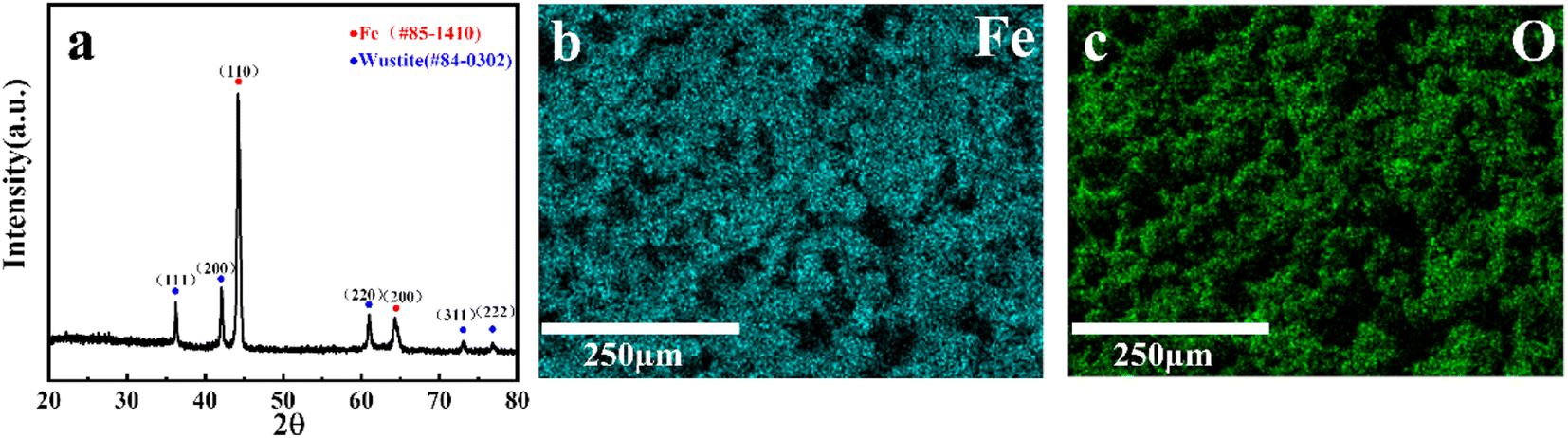 | ||
| Fig. 3 (a) XRD profiles and (b and c) EDS images of Fe–Fe1−xO integrative electrodes. | ||
The electrochemical properties of Fe based electrodes before or after rusted by the EDR technique were investigated in three electrodes system using cyclic voltammetry (CV) in 1 M KOH solution in a potential range of −0.8 V to 0 V versus Hg/HgO. From Fig. 4a, it is obvious that the Fe based electrode before EDR processing showed very small current response, whereas the Fe based electrode after EDR treatment gained a much higher current density at the same scanning rate of 100 mV s−1. These phenomena were also observed at various scanning rates of 10, 20, 50 and 200 mV s−1 (Fig. 4b and c). The areal capacitances of the Fe based electrodes before or after EDR processing were estimated from the CV curves. As shown in Fig. 4d, the areal capacitances of the Fe based electrodes after EDR processing were much higher than those without EDR processing at all testing conditions. For instance, Fe based electrode after EDR processing showed a high areal capacitance of 51.3 mF cm−2 at 10 mV s−1, which was 26 times larger than that without EDR processing at the same testing scanning rate. The improved capacitance is attributed to the high capacitance of Fe1−xO microsphere particles, which formed a porous microstructure. The microstructure of active materials provides sufficient surface area for efficient redox reactions. Moreover, the Fe–Fe1−xO integrative electrode design without adding any low conductivity binder and conductive media facilitated rapid electron transportation during charge–discharge processes.
 | ||
| Fig. 4 (a) CV curves of Fe based electrodes before EDR and after EDR at 100 mV s−1, (b) CV curves of Fe metal electrode before EDR, (c) CV curves of Fe metal electrode after EDR and (d) corresponding areal capacitance of Fe based electrodes before EDR and after EDR. | ||
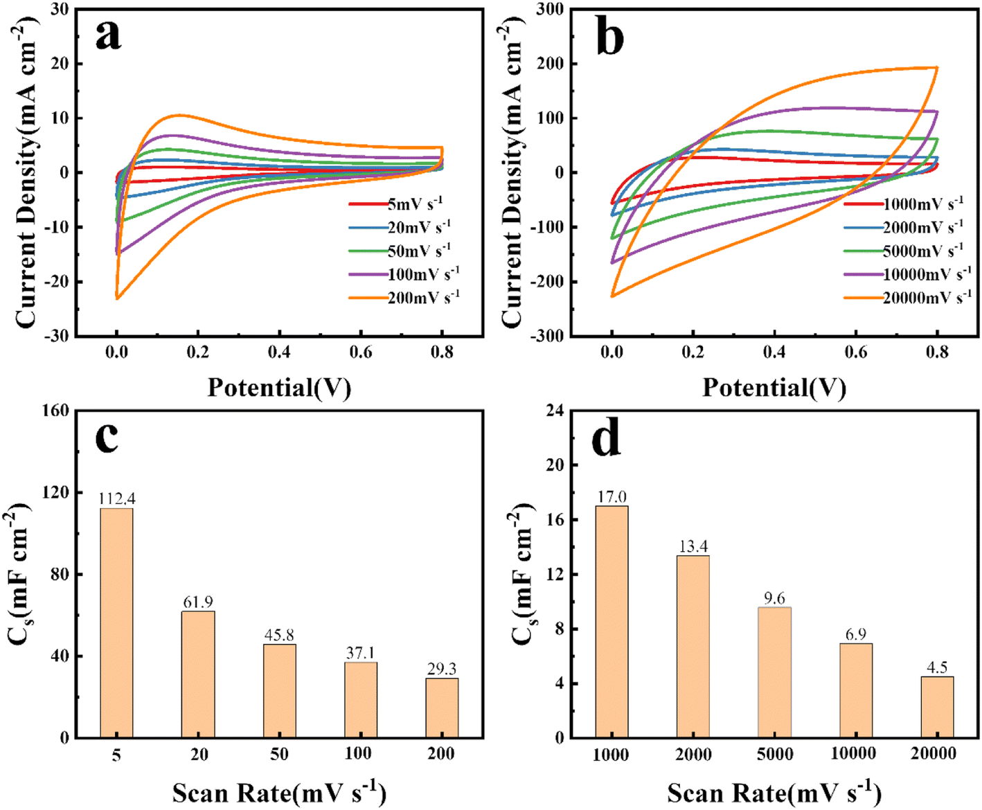
The Fe–Fe1−xO integrative electrodes were machined into square maze 3D CMSC devices with different orbits (such as T-CMSC and F-CMSC, shown in Fig. 1b and c). These Fe– Fe1−xO based square maze 3D CMSC devices were examined at a testing voltage range from 0 to 0.8 V in 1 M KOH electrolyte and the applied scanning rates ranging from 5 to 20000 mV s−1. Fig. 5 presented the CV testing results of T-CMSC and F-CMSC obtained at relatively low applied scanning rates ranged from 5 to 200 mV s−1. From Fig. 5a, it is found that the current response of F-CMSC was much higher than that of T-CMSC at the same testing condition of 100 mV s−1. The same phenomena were observed for T-CMSC and F-CMSC at other applied scanning rates, which were displayed in Fig. 5b and c, respectively. Fig. 5d exhibits the areal capacitances of T-CMSC and F-CMSC obtained from corresponding CV curves in Fig. 5b and c. It is seen that the F-CMSC device showed remarkably higher areal capacitances than the T-CMSC device at all applied scanning rates. The highest areal capacitance values gained at 5 mV s−1 for T-CMSC and F-CMSC were 27.1 and 45 mF cm−2, respectively. At a higher scanning rate of 200 mV s−1, the areal capacitance value obtained for F-CMSC was 17.5 mF cm−2, whereas T-CMSC showed only 4.6 mF cm−2. This implied that F-CMSC with small electrode width was more beneficial for storing energy compared to T-CMSC, especially at relatively high applied scanning rates. In order to further prove the advantages of the Fe–Fe1−xO based integrative devices, prepared by EDR, the T-CMSC and F-CMSC microdevices were examined at superhigh scanning rates from 1000 to 20000 mV s−1. Fig. 6 presents the CV testing results of T-CMSC and F-CMSC obtained at these superhigh scanning rates. From Fig. 6a, it is easy to find that the current response of F-CMSC was also much higher than that of T-CMSC at 1000 mV s−1, which correlates with testing results at 100 mV s−1. The same phenomena were also observed for T-CMSC and F-CMSC at other ultra-high applied scanning rates, as it is shown in Fig. 6b and c, respectively. It is important to note that CV curves for T-CMSC and F-CMSC maintained a good box shape at these ultra-high applied scanning rates (1000–20000 mV s−1), which indicated that the fabricated Fe–Fe1−xO based integrative devices by EDR achieved good capacitive behavior. Fig. 6d described the areal capacitances of T-CMSC and F-CMSC obtained from corresponding CV curves in Fig. 6b and c. The F-CMSC device achieved a remarkably higher areal capacitance than the T-CMSC device at all applied scanning rates. When the scanning rate increased to 20000 mV s−1, the areal capacitance value obtained for F-CMSC was still as high as 3.5 mF cm−2. This is because F-CMSC with small electrode width and porous microstructure facilitated efficient ion transport and the binder-free Fe–Fe1−xO integrative electrode design facilitated the electron transport. In order to further study the capacitive behavior of F-CMSC devices with five orbits, GCD characterization was carried out with different applied current densities (0.2 to 5 mA cm−2) at a voltage window of 0–0.8 V. The GCD curves showed a symmetric triangle configuration at all examined current densities (Fig. 7a and b), which indicated that good capacitive performance was achieved for F-CMSC devices. The corresponding capacitance values calculated from the GCD curves were presented in Fig. 7c and d. A maximum areal capacitance of 33.6 mF cm−2 was obtained at a current density of 0.2 mA cm−2. The areal capacitance value decreased with the increase of current density. It is important to find that F-CMSC devices still maintained a high areal capacitance of 6.3 mF cm−2 at a high current density of 5 mA cm−2. This is attributed to the high theoretical capacitance of iron oxide particles, advanced microstructures generated by EDR, binder-free electrode design and small electrode width, which were greatly helpful for ion and electron migration and obtaining enhanced capacitive performance.
 | ||
| Fig. 5 (a) CV curves of Fe–Fe1−xO based T-CMSC and F-CMSC at 100 mV s−1, (b and c) CV curves of Fe–Fe1−xO based (b) T-CMSC and (c) F-CMSC, respectively, and (d) corresponding areal capacitance of Fe–Fe1−xO based T-CMSC and F-CMSC (applied scanning rates: 5–200 mV s−1). | ||
 | ||
| Fig. 6 (a) CV curves of Fe–Fe1−xO based T-CMSC and F-CMSC at 1000 mV s−1, (b and c) CV curves of Fe–Fe1−xO based (b) T-CMSC and (c) F-CMSC, respectively, and (d) corresponding areal capacitance of Fe–Fe1−xO based T-CMSC and F-CMSC (applied scanning rates: 1000–20000 mV s−1). | ||
 | ||
| Fig. 7 GCD curves of Fe–Fe1−xO based F-CMSC at applied current densities of (a) 0.2–0.7 mA cm−2 and (b) 0.9–5 mA cm−2, respectively, and (c and d) areal capacitance of F-CMSC obtained from corresponding GCD curves. | ||
More importantly, aiming to examine the advantage of the EDR manufacturing technique for fabricating there-dimensional CMSC devices, thicker Fe pure metal substrates with a thickness of 2 mm were adopted as the original materials for fabricating 3D CMSC devices with five orbits (named as 2F-CMSC). Fig. 8a and b present the CV curves for 3D 2F-CMSC devices at low scan rates of 5–200 mV s−1 and high scan rates of 1000–20000 mV s−1, respectively. The results showed that all the CV curves maintained a rectangle configuration at all scanning rates, which indicated that good capacitive behavior was obtained for 3D 2F-CMSC devices. The corresponding capacitance value calculated from the CV curves were presented in Fig. 8c and d. The 3D 2F-CMSC devices achieved a maximum areal capacitance of 112.4 mF cm−2 (5 mV s−1), which is 2.5 times higher than that obtained for F-CMSC, which is just 45 mF cm−2 (5 mV s−1) (Fig. 5d). It is suggested that the thicker 3D electrode configuration enabled for loading more active materials and providing more active sites for charge accumulation. Moreover, these obtained values of areal capacitance for 3D 2F-CMSC in this work were larger than many other reported values in literature for coplanar microsupercapacitors, such as V-doped BiFeO3//PPy asymmetric CMSC (10 mF cm−2 at 20 mV s−1) fabricated by the combination of electrochemical deposition, electrophoretic deposition and chemical polymerization methods,39 CuHCF-CNT//Fe2O3-CNT asymmetric CMSC (15 mF cm−2 at 200 mV s−1) fabricated by the combination of laser engraving and capillary force assisted printing methods,40 RuO2//Ti3C2Tx asymmetric CMSC (60 mF cm−2 at 5 mV s−1) fabricated by the combination of laser cutting and hydrothermal methods,41 and MnO2//VN asymmetric CMSC (16.1 mF cm−2 at 1 mV s−1) fabricated by the combination of chemical precipitation and mask-assisted filtration.42 Therefore, it is important to mention that the EDR technique proposed in this work not only greatly simplified the manufacturing process for high performance 3D CMSC devices, but also successfully eliminated complicated pretreatment and posttreatment processing, and avoided the usage of low conductive binder, conductive media, hazardous solvent, additional current collector and expensive manufacturing equipment. Additionally, Fig. 8c and d showed that the areal capacitance value decreased with the increasing scanning rate. The rate capacity of 3D 2F-CMSC was 33% when the scanning rate increased from 5 to 100 mV s−1. More importantly, the 3D 2F-CMSC devices still maintained a high areal capacitance of 4.5 mF cm−2 at a superhigh scanning rate of 20000 mV s−1, and the capacitance ratio of 4% was still achieved even when the applied scanning rate has been increased up to 4000-folds of the initial value. It is important to note that the metal oxide based coplanar microsupercapacitors fabricated by other techniques in the literature normally could be operated only at relatively low scanning rates below 200 mV s−1 (ref. 43–45). Even at such low applied scanning rates, their CV curves showed deviation from a rectangle shape, which indicated poor capacitive performance at high applied scanning rates. In contrast, it is easy to find that the 3D 2F-CMSC device fabricated by one-step EDR strategy show good capacitive properties at a superhigh scanning rate of 20000 mV s−1 (Fig. 8b), which was 100 times higher than those used in the literature.39,43–45 Moreover, the 2F-CMSC device showed 81.67% capacitance retention after 2000 cycles at a scan rate of 500 mV s−1 (Fig. 1S†). More importantly, the good capacitive performance at superhigh applied scanning rates was achieved without any conducting additives. Subsequently, GCD characterization was conducted to study the capacitive performance of 3D 2F-CMSC devices with applied current densities of 0.2–5 mA cm−2 at a voltage window of 0–0.8 V. The GCD curves showed a symmetric triangle shape at all examined current densities (Fig. 9a and b), which indicated that good capacitive performance was achieved for 2F-CMSC devices. The corresponding capacitance value calculated from the GCD curves were presented in Fig. 9c and d. A maximum areal capacitance of 51.2 mF cm−2 was obtained at 0.2 mA cm−2, which was larger than reported areal capacitance values of CMSC devices, such as CuSe@FeOOH//CuSe@MnOOH CMSC (20.5 mF cm−2 at 0.11 mA cm−2) fabricated by combining photolithography and electrodeposition methods,45 Co(OH)2//VN hybrid CMSC (21 mF cm−2 at 0.2 mA cm−2) fabricated by combining chemical precipitation, electrochemical exfoliation and vacuum filtration methods,44 and MnO2-graphite//graphite CMSC (220 µF cm−2 at 2.5 µA cm−2) fabricated by combining simple pencil drawing and electrodeposition methods.43 The areal capacitance value decreased as the current density increased. It is important to mention that 3D 2F-CMSC devices still maintained a high areal capacitance of 12.5 mF cm−2 at a high current density of 5 mA cm−2. This is attributed to the high theoretical capacitance of iron oxide particles, advanced microstructures generated by EDR, binder-free electrode configuration design, 3D current collector configuration design and small electrode width, which were greatly helpful for ion/electron migration and making full use of Fe1−xO active materials, and thus enhanced capacitive performance of 3D 2F-CMSC devices was achieved. In addition, the one-step EDR strategy proposed in this work was able to fabricate 3D CMSC devices with various designable patterns drawed by the CAD software, and the whole manufacturing procedures could be automatically controlled by computer numerical control system, which could improve the fabrication efficiency and reduce the manpower as well as resources. Moreover, as the fabricating process of EDR eliminated the utilization of toxic solvents, it offers health and environmental benefits. The developed one-step EDR technique in this research paves the way for synthesis of different metal oxide based materials for various applications, such as lithium-ion batteries, catalysts, sensors, water splitting and drug delivery.
 | ||
| Fig. 8 CV curves of Fe–Fe1−xO based 2F-CMSC at applied scanning rates of (a) 5–200 mV s−1 and (b) 1000–20000 mV s−1, respectively, and (c and d) areal capacitance of 2F-CMSC obtained from corresponding CV curves. | ||
 | ||
| Fig. 9 GCD curves of Fe–Fe1−xO based 2F-CMSC at applied current densities of (a) 0.2–0.7 mA cm−2 and (b) 0.9–5 mA cm−2, respectively, and (c and d) areal capacitance of 2F-CMSC obtained from corresponding GCD curves. | ||
4. Conclusions
EDR has been developed for the first time for direct one-step growth of wustite (Fe1−xO) layer on the iron substrate in deionized water for supercapacitor application. The fabricated Fe–Fe1−xO based integrative electrodes and 3D CMSC devices developed by this facile, simple, scalable, binder-free, surfactant-free and conductive additive-free EDR strategy showed an excellent capacitive performance. The fabricated Fe–Fe1−xO based electrode exhibited an areal capacitance of 51.3 mF cm−2 at 10 mV s−1, which is 26 times higher than that of the pure iron electrodes without EDR treatment. Moreover, the 3D CMSC devices with different patterns could be directly fabricated by EDR, which is automatically controlled by computer-aided design. It was also found that microelectrodes with smaller width were beneficial for enhancing the capacitive performance of the 3D CMSC devices due to the reduction of ion transfer distance. The fabricated Fe–Fe1−xO based 3D 2F-CMSC devices achieved a maximum areal capacitance of 112.4 mF cm−2 at 5 mV s−1. The 3D 2F-CMSC device showed a good capacitive behavior and achieved a high areal capacitance of 4.5 mF cm−2 at an ultra high scan rate of 20000 mV s−1, which resulted from the integrated electrode design. The approach allowed for elimination of binder and conductive media, which are used in traditional fabrication process, and the 3D electrode configuration design facilitated fast ion/electronic transport. The results proved that EDR is a low-cost strategy for rapid and large-scale fabrication of high performance supercapacitor integrative electrodes and devices. Moreover, it is a versatile technique that showed a great potential for developing other next generation microelectronic devices, such as microbatteries and microsensors.
Conflicts of interest
There are no conflicts to declare.Acknowledgements
The authors express their appreciation for National Natural Science Foundation of China (Grant numbers 52002085 and U22A2062), Education Department of Guangdong Province (Grant numbers 2022KTSCX069 and 2021ZDZX4039), Research Start-up Funds of Guangdong Polytechnic Normal University (Grant numbers 2021SDKYA106 and 2022SDKYB027), Guangdong Province Modern Agricultural Industrial Technology System (Grant number 2019KJ139), Jiangxi Province Major Research and Development Projects (Grant number 20223AAE02008), Guangzhou Basic and Applied Basic Research Foundation (Grant number 2023A04J0278), Guangdong Province Science and Technology Innovation Strategy Special Fund (Grant number pdjh2023b0311), Guangdong Province Nature Science Foundation of China (Grant number 2022A1515011065) and Organized Scientific Research Project of Guangdong Polytechnic Normal University (Grant number 22GPNUZDJS21).References
- C. Zhao, Y. Liu, S. Beirne, J. Razal and J. Chen, Recent development of fabricating flexible micro‐supercapacitors for wearable devices, Adv. Mater. Technol., 2018, 3(9), 1800028 CrossRef.
- J. Zhang, G. Zhang, T. Zhou and S. Sun, Recent developments of planar micro‐supercapacitors: fabrication, properties, and applications, Adv. Funct. Mater., 2020, 30(19), 1910000 CrossRef CAS.
- X. Wang and Q. Zhang, On‐chip microsupercapacitors: from material to fabrication, Energy Technol., 2019, 7(11), 1900820 CrossRef CAS.
- C. Shao, Y. Zhao and L. Qu, Recent advances in highly integrated energy conversion and storage system, SusMat, 2022, 2(2), 142–160 CrossRef CAS.
- F. Bu, W. Zhou, Y. Xu, Y. Du, C. Guan and W. Huang, Recent developments of advanced micro-supercapacitors: Design, fabrication and applications, npj Flexible Electron., 2020, 4(1), 31 CrossRef.
- Z. Zhu, R. Kan, S. Hu, L. He, X. Hong, H. Tang and W. Luo, Recent Advances in High‐Performance Microbatteries: Construction, Application, and Perspective, Small, 2020, 16(39), 2003251 CrossRef CAS PubMed.
- L. Liu, H. Zhao and Y. Lei, Advances on three‐dimensional electrodes for micro‐supercapacitors: a mini‐review, InfoMat, 2019, 1(1), 74–84 CrossRef CAS.
- W. Zong, Y. Ouyang, Y.-E. Miao, T. Liu and F. Lai, Recent advances and perspectives of 3D printed micro-supercapacitors: from design to smart integrated devices, Chem. Commun., 2022, 58(13), 2075–2095 RSC.
- D. Qi, Y. Liu, Z. Liu, L. Zhang and X. Chen, Design of architectures and materials in in‐plane micro‐supercapacitors: current status and future challenges, Adv. Mater., 2017, 29(5), 1602802 CrossRef PubMed.
- C. Shen, S. Xu, Y. Xie, M. Sanghadasa, X. Wang and L. Lin, A review of on-chip micro supercapacitors for integrated self-powering systems, J. Microelectromech. Syst., 2017, 26(5), 949–965 CAS.
- N. Kurra, B. Ahmed, Y. Gogotsi and H. N. Alshareef, MXene‐on‐paper coplanar microsupercapacitors, Adv. Energy Mater., 2016, 6(24), 1601372 CrossRef.
- Z.-S. Wu, K. Parvez, X. Feng and K. Müllen, Photolithographic fabrication of high-performance all-solid-state graphene-based planar micro-supercapacitors with different interdigital fingers, J. Mater. Chem. A, 2014, 2(22), 8288–8293 RSC.
- S.-W. Zhang, B.-S. Yin, C. Liu, Z.-B. Wang and D.-M. Gu, Self-assembling hierarchical NiCo2O4/MnO2 nanosheets and MoO3/PPy core-shell heterostructured nanobelts for supercapacitor, Chem. Eng. J., 2017, 312, 296–305 CrossRef CAS.
- J. Qin, P. Das, S. Zheng and Z.-S. Wu, A perspective on two-dimensional materials for planar micro-supercapacitors, APL Mater., 2019, 7(9), 090902 CrossRef.
- L. Liu, H.-Y. Li, Y. Yu, L. Liu and Y. Wu, Silver nanowires as the current collector for a flexible in-plane micro-supercapacitor via a one-step, mask-free patterning strategy, Nanotechnology, 2018, 29(5), 055401 CrossRef PubMed.
- Z.-S. Wu, Y.-Z. Tan, S. Zheng, S. Wang, K. Parvez, J. Qin, X. Shi, C. Sun, X. Bao and X. Feng, Bottom-up fabrication of sulfur-doped graphene films derived from sulfur-annulated nanographene for ultrahigh volumetric capacitance micro-supercapacitors, J. Am. Chem. Soc., 2017, 139(12), 4506–4512 CrossRef CAS PubMed.
- W. J. Hyun, E. B. Secor, C. H. Kim, M. C. Hersam, L. F. Francis and C. D. Frisbie, Scalable, self‐aligned printing of flexible graphene micro‐supercapacitors, Adv. Energy Mater., 2017, 7(17), 1700285 CrossRef.
- Y. Chen, X. Li, Z. Bi, G. Li, X. He and X. Gao, Stamp-assisted printing of nanotextured electrodes for high-performance flexible planar micro-supercapacitors, Chem. Eng. J., 2018, 353, 499–506 CrossRef CAS.
- X. Shi, S. Pei, F. Zhou, W. Ren, H.-M. Cheng, Z.-S. Wu and X. Bao, Ultrahigh-voltage integrated micro-supercapacitors with designable shapes and superior flexibility, Energy Environ. Sci., 2019, 12(5), 1534–1541 RSC.
- J.-Q. Xie, Y.-Q. Ji, J.-H. Kang, J.-L. Sheng, D.-S. Mao, X.-Z. Fu, R. Sun and C.-P. Wong, In situ growth of Cu(OH)2@FeOOH nanotube arrays on catalytically deposited Cu current collector patterns for high-performance flexible in-plane micro-sized energy storage devices, Energy Environ. Sci., 2019, 12(1), 194–205 RSC.
- R. Chen and I. Zhitomirsky, Colloidal methods for the fabrication of Mn3O4-graphene film and bulk supercapacitors, Mater. Lett., 2023, 335, 133811 CrossRef CAS.
- R. Chen, Z. Wang, R. Sahu, I. Puri and I. Zhitomirsky, Influence of molecular structure of extractor molecules on liquid-liquid extraction of oxide particles and properties of composites, Ceram. Int., 2018, 44(13), 15714–15720 CrossRef CAS.
- J. Wang, F. Li, F. Zhu and O. G. Schmidt, Recent progress in micro‐supercapacitor design, integration, and functionalization, Small Methods, 2019, 3(8), 1800367 Search PubMed.
- S. S. Delekta, K. H. Adolfsson, N. B. Erdal, M. Hakkarainen, M. Östling and J. Li, Fully inkjet printed ultrathin microsupercapacitors based on graphene electrodes and a nano-graphene oxide electrolyte, Nanoscale, 2019, 11(21), 10172–10177 RSC.
- K.-H. Choi, J. Yoo, C. K. Lee and S.-Y. Lee, All-inkjet-printed, solid-state flexible supercapacitors on paper, Energy Environ. Sci., 2016, 9(9), 2812–2821 RSC.
- W. Yu, H. Zhou, B. Q. Li and S. Ding, 3D printing of carbon nanotubes-based microsupercapacitors, ACS Appl. Mater. Interfaces, 2017, 9(5), 4597–4604 CrossRef CAS PubMed.
- K. Shen, J. Ding and S. Yang, 3D printing quasi‐solid‐state asymmetric micro‐supercapacitors with ultrahigh areal energy density, Adv. Energy Mater., 2018, 8(20), 1800408 CrossRef.
- R. Chen, M. Yu, R. P. Sahu, I. K. Puri and I. Zhitomirsky, The development of pseudocapacitor electrodes and devices with high active mass loading, Adv. Energy Mater., 2020, 10(20), 1903848 CrossRef CAS.
- L. Li, J. Zhang, Z. Peng, Y. Li, C. Gao, Y. Ji, R. Ye, N. D. Kim, Q. Zhong and Y. Yang, High-Performance Pseudocapacitive Microsupercapacitors from Laser-Induced Graphene, Adv. Mater., 2015, 28(5), 838–845 CrossRef PubMed.
- W. Gao, N. Singh, L. Song, Z. Liu, A. L. M. Reddy, L. Ci, R. Vajtai, Q. Zhang, B. Wei and P. M. Ajayan, Direct laser writing of micro-supercapacitors on hydrated graphite oxide films, Nat. Nanotechnol., 2011, 6(8), 496–500 CrossRef CAS PubMed.
- J. Lin, Z. Peng, Y. Liu, F. Ruiz-Zepeda, R. Ye, E. L. Samuel, M. J. Yacaman, B. I. Yakobson and J. M. Tour, Laser-induced porous graphene films from commercial polymers, Nat. Commun., 2014, 5(1), 5714 CrossRef CAS PubMed.
- C. Lethien, J. Le Bideau and T. Brousse, Challenges and prospects of 3D micro-supercapacitors for powering the internet of things, Energy Environ. Sci., 2019, 12(1), 96–115 RSC.
- F. Xin, Y. Jia, J. Sun, L. Dang, Z. Liu and Z. Lei, Enhancing the capacitive performance of carbonized wood by growing FeOOH nanosheets and poly (3, 4-ethylenedioxythiophene) coating, ACS Appl. Mater. Interfaces, 2018, 10(38), 32192–32200 CrossRef CAS PubMed.
- S. H. Park, G. Goodall and W. S. Kim, Perspective on 3D-designed micro-supercapacitors, Mater. Des., 2020, 193, 108797 CrossRef CAS.
- X. Zeng, L. Zhu, B. Yang and R. Yu, Necklace-like Fe3O4 nanoparticle beads on carbon nanotube threads for microwave absorption and supercapacitors, Mater. Des., 2020, 189, 108517 CrossRef CAS.
- Y. Zhang, Y. Liu, R. Ji and B. Cai, Study of the recast layer of a surface machined by sinking electrical discharge machining using water-in-oil emulsion as dielectric, Appl. Surf. Sci., 2011, 257(14), 5989–5997 CrossRef CAS.
- W. Zhang, F. Wang, X. Li, Y. Liu, Y. Liu and J. Ma, Fabrication of hollow carbon nanospheres introduced with Fe and N species immobilized palladium nanoparticles as catalysts for the semihydrogenation of phenylacetylene under mild reaction conditions, Appl. Surf. Sci., 2017, 404, 398–408 CrossRef CAS.
- S. Lentijo-Mozo, D. Deiana, E. Sogne, A. Casu and A. Falqui, Unexpected insights about cation-exchange on metal oxide nanoparticles and its effect on their magnetic behavior, Chem. Mater., 2018, 30(21), 8099–8112 CrossRef CAS.
- Q. Pan, C. Yang, W. Qi, H. Wei, R. Ling, N. Jiao, S. Yang, X. Li and B. Cao, Electrochemically constructing V-doped BiFeO3 nanoflake network anodes for flexible asymmetric micro-supercapacitors, Electrochim. Acta, 2021, 393, 139079 CrossRef CAS.
- J. Li, Y. Shao, C. Hou, Q. Zhang, Y. Li and H. Wang, Capillary force driven printing of asymmetric Na-ion micro-supercapacitors, J. Mater. Chem. A, 2020, 8(42), 22083–22089 RSC.
- Q. Jiang, N. Kurra, M. Alhabeb, Y. Gogotsi and H. N. Alshareef, All pseudocapacitive MXene‐RuO2 asymmetric supercapacitors, Adv. Energy Mater., 2018, 8(13), 1703043 CrossRef.
- J. Qin, S. Wang, F. Zhou, P. Das, S. Zheng, C. Sun, X. Bao and Z.-S. Wu, 2D mesoporous MnO2 nanosheets for high-energy asymmetric micro-supercapacitors in water-in-salt gel electrolyte, Energy Storage Mater., 2019, 18, 397–404 CrossRef.
- L. Yao, T. Cheng, X. Shen, Y. Zhang, W. Lai and W. Huang, based all-solid-state flexible asymmetric micro-supercapacitors fabricated by a simple pencil drawing methodology, Chin. Chem. Lett., 2018, 29(4), 587–591 CrossRef CAS.
- S. Wang, Z.-S. Wu, F. Zhou, X. Shi, S. Zheng, J. Qin, H. Xiao, C. Sun and X. Bao, All-solid-state high-energy planar hybrid micro-supercapacitors based on 2D VN nanosheets and Co(OH)2 nanoflowers, npj 2D Mater. Appl., 2018, 2(1), 7 CrossRef.
- N. Hillier, S. Yong and S. Beeby, The good, the bad and the porous: A review of carbonaceous materials for flexible supercapacitor applications, Energy Rep., 2020, 6, 148–156 CrossRef.
Footnote |
| † Electronic supplementary information (ESI) available. See DOI: https://doi.org/10.1039/d3ra04838a |
| This journal is © The Royal Society of Chemistry 2023 |