DOI:
10.1039/D3RA04823C
(Review Article)
RSC Adv., 2023,
13, 33797-33819
Dopant engineering for ZnO electron transport layer towards efficient perovskite solar cells
Received
18th July 2023
, Accepted 30th October 2023
First published on 17th November 2023
Abstract
The conventional electron transport layer (ETL) TiO2 has been widely used in perovskite solar cells (PSCs), which have produced exceptional power conversion efficiencies (PCE), allowing the technology to be highly regarded and propitious. Nevertheless, the recent high demand for energy harvesters in wearable electronics, aerospace, and building integration has led to the need for flexible solar cells. However, the conventional TiO2 ETL layer is less preferred, where a crystallization process at a temperature as high as 450 °C is required, which degrades the plastic substrate. Zinc oxide nanorods (ZnO NRs) as a simple and low-cost fabrication material may fulfil the need as an ETL, but they still suffer from low PCE due to atomic defect vacancy. To delve into the issue, several dopants have been reviewed as an additive to passivate or substitute the Zn2+ vacancies, thus enhancing the charge transport mechanism. This work thereby unravels and provides a clear insight into dopant engineering in ZnO NRs ETL for PSC.
1. Introduction
Solar energy is an essential primary energy source that continues to gain worldwide recognition for providing energy to human life. In comparison to fossil fuels, solar energy is regarded as the key renewable energy source that assists in reducing greenhouse gas emissions and curbing climate change. Consequently, solar energy technology has received considerable attention, and the solar industry has experienced enormous expansion and sustainable development globally. According to the International Energy Agency (IEA), solar energy continues to be the most prominent among all renewable energy sources with the highest growth of net renewable power capacity over the past 5 years, as illustrated in Fig. 1. Solar energy has dominated more than half of all other technologies and is expected to grow significantly in the future.1
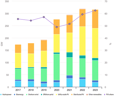 |
| | Fig. 1 The growth in the net renewable power capacity by different technologies. Data derived from the International Renewable Energy Agency report.1 | |
Solar cells and other photovoltaic (PV) devices generate power directly from sunlight, which applies the photovoltaic effect. Energy in the form of photons from the sun is absorbed and excites the electrons and produces a current that generates electricity. In general, solar cell technology is categorized into three generations, with single and multi-crystalline silicon-based solar cells from the first generation being the most prevalent and widely available on the market. In response to the excessive material consumption and expense of silicon solar cells, second-generation solar cells have been developed, where the maximum layer thickness has been reduced to a nanometer scale, thereby reducing the amount of materials used. Meanwhile, numerous researchers have experimented with the concept of light control utilising dye-sensitive solar cells (DSSCs), perovskite, organic solar cells, quantum dots (QDs), nanostructuring, and nanopatterning, which is considered the third-generation solar cell. This technology, referred to as emerging photovoltaic technology, has been studied extensively for 25 years but has not yet been widely marketed owing to poor cell performance and instability limitations. Nevertheless, emerging photovoltaic technologies offer more competitive fabrication costs, allowing for mass marketing and are also superior in generating energy at low wavelengths, therefore being suitable for indoor use.
Recent developments have demonstrated the prowess of PSCs among other solar cells, which have shown a significant rise in the performance in less than a decade, as displayed in Fig. 2.2 This clearly indicates the great potential of PSCs to develop and revolutionize the renewable energy technology. Nevertheless, PSC-related research has largely focused on the perovskite absorber layer and the hole transport layer (HTL), and has designated the mesoporous TiO2 layer as the ETL. Although TiO2 ETL has proven its superiority in terms of efficiency, stability and cost-effectiveness, there is still room for improvement in continuing to improve the overall PSC performance. The ETL plays an important role in facilitating the efficient extraction and transport of electrons from the perovskite absorber to the external circuit. In spite of that, the addition of dopant elements or dopant engineering in ETL offers a viable route in promoting a more efficient charge transport mechanism by means of passivating or replacing the bulk defects in the ETL layer. This allows a way to tailor the layer properties and increase the full potential of that ETL layer, thereby improving the device performance.
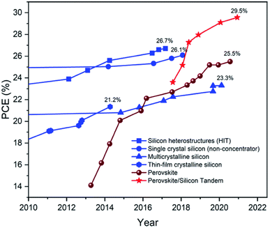 |
| | Fig. 2 The evolution of silicon, perovskite, and perovskite–silicon tandem device efficiency over the past decade, as derived from the efficiency table published by the National Renewable Energy Laboratory. This figure has been reproduced from ref. 2 with permission from the Royal Society of Chemistry, copyright 2021. | |
2. Emerging perovskite photovoltaic
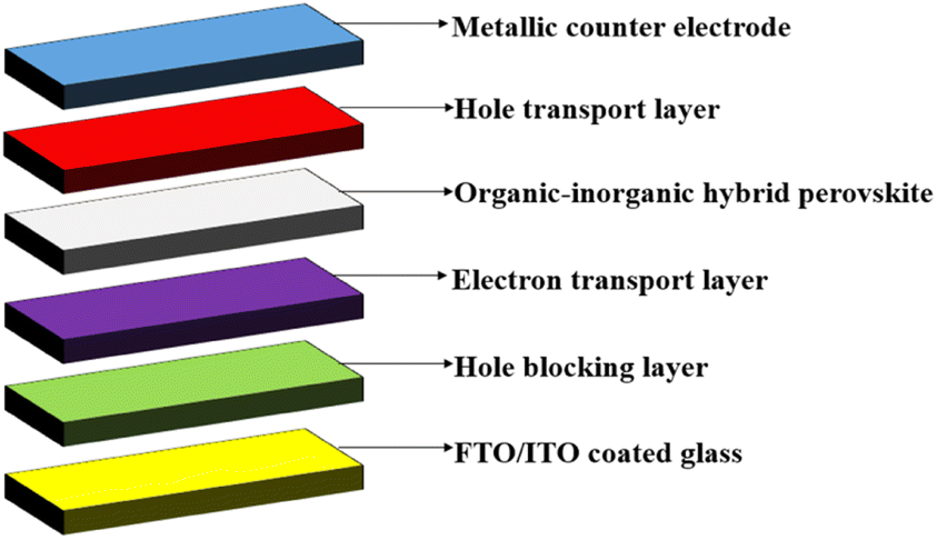
The PSCs layers of materials are printed, coated, or vacuum-deposited onto a support layer beneath the perovskite cell, known as the substrate in order to construct the cells. For the most part, they are simple to construct and able to achieve efficiency levels comparable to crystalline silicon. For the record, the PSC efficiency has increased from merely 3% in 2009 to over 25% by 2020, demonstrating a dramatic rise as a newly introduced solar cell. PSCs are based on the solid-state dye-sensitized solar cell technology introduced by Gratzel. In 1991, O'Regan and Gratzel invented a low-cost photoelectrochemical solar cell, in which nanocrystalline TiO2 films were sensitized and reacted with the molecular dyes.3 In 2009, a methylammonium lead halide perovskite was introduced as an absorbent layer in a liquid-based DSSC, which successfully reacted with a nanocrystalline TiO2 layer, resulting in a PCE of only 3–4%.4 Two years later, the structure was named as a PSC, as shown in Fig. 3, and has shown a dramatic improvement in performance, increasing in PCE value by two-folds.4 The front contact is formed from an FTO substrate, stacked up with a layered material structure comprising an ETL, a perovskite layer and a HTL. The electron and HTL provide a charge carrier conduction layer, while the perovskite material absorbs photons, depending on the wavelength range correlated with the bandgap of the material.
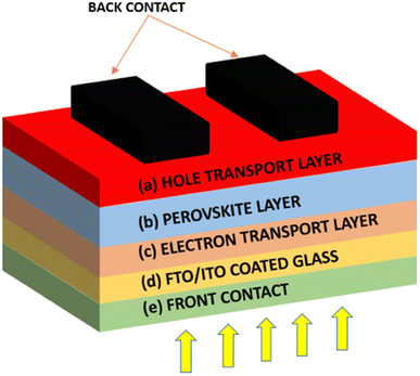 |
| | Fig. 3 A basic schematic diagram of PSC: (a) hole transport layer, (b) perovskite layer, (c) electron transport layer, (d) FTO/ITO coated glass, and (e) front contact. | |
Usually, conventional PSCs are in liquid-based form, using Spiro Ometad as the HTL layer. However, these PSCs are still hampered by stability concerns, especially the immediate dissolution of the perovskite material in the liquid-based electrolyte. To address this issue, some researchers proposed the idea of substituting the liquid-based electrolyte with a solid-state perovskite conductor. As a result, a PCE value of 10% was reached in 2012, and continued to rise as high as 18% in less than 2 years, manifesting the great potential of the structure. The stability issue has also been resolved, where cells can function efficiently for long periods of time.4 Recently, using low-cost organometal halides combined with silver nanoparticles (AgNPs) as HTL in PSCs, Elseman et al. produced good PCE values exceeding 20%. The success achieved in this short period of time shows the high potential of the use of inorganic HTL materials in reducing fabrication costs and alleviating PSC reliability, even improving the PCE value.5
In general, solar cells are built as PIN diodes, where one part will be the HTL (p-type) and the other part will be the ETL (n-type). In the basic structure of a PSC as shown in Fig. 3, a perovskite layer (i) is sandwiched between a HTL (p) and an ETL (n), followed by other layers consisting of the FTO/ITO coated glass, back contact and front contact. The HTL and ETL both must have high conductivity, so that the energy level of both layers are properly aligned with the photoactive perovskite layer. The HTL in p–i–n architectures plays an important role in: (i) extracting and transporting holes from the active layer to the electrode; (ii) blocking the transfer of electrons to the anode; (iii) optimizing device stability by reducing the risk of degradation and corrosion; and (iv) increasing the open-circuit voltage (Voc) of the well-matched HOMO energy level.6,7 Meanwhile, the ETL in n–i–p architectures also plays a crucial role in the fabrication of high-performance PSC by: (i) transporting photogenerated electrons from the PSC layer to the cathode or anode, and (ii) modifying the contact between the perovskite layer and the electrode to reduce charge recombination.8,9 The development of a high performance HTL for PSC was reported using MEA (monoethanolamine) as the solvent for CuI (copper(I) iodide), demonstrating the effectiveness of combining the solvent and annealing temperature to obtain desirable CuI structures. The utilization of MEA as a solvent enables the simple, inexpensive, and rapid preparation of HTL films, ultimately reducing the cost of solar cell production.10 Besides that, the simulations were conducted using SCAPS modelling software to analyse the impact of various parameters on the PSC performance. The authors focused on the thickness, doping, operating temperature, and interface defect of different HTLs and absorber layers. The simulations revealed that an inorganic material and Cu2O in the HTL yielded the highest PCE value of 17.71%, surpassing other HTL materials. Furthermore, using a CH3NH3SnI3 absorber layer, a PCE value as high as 27.72% was achieved, enabling its potential as a replacement for CH3NH3PbI3 due to its higher efficiency and being Pb-free and cost-effective.11
Apart from HTL and ETL layers, the transport mechanism (diffusion) of the charge carrier in PSC materials is one of the important components of a highly efficient PSC. The net movement of the particles (holes and electrons) induced by the density gradient is called diffusion, where the diffusion of these particles involves the movement of either holes or electrons to locations with lower densities, as described in Fig. 4(a). The diffusion will exist as long as there is a concentration gradient in the particles, and it can be described by Fick's law of diffusion:12
| |
 | (1) |
Je – electron current density,
q – elementary charge,
De – diffusion coefficient,

– density gradient in the direction of
x.
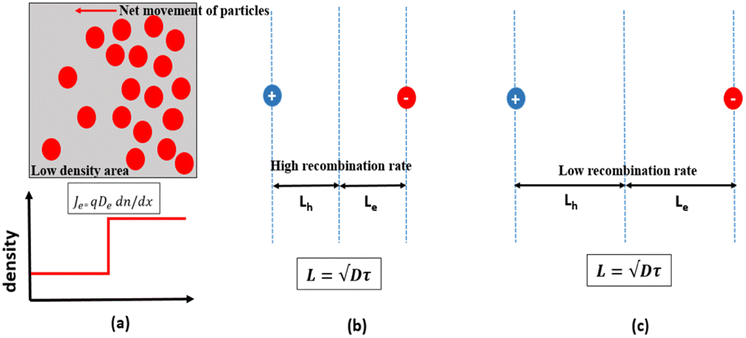 |
| | Fig. 4 (a) The diffusion of particles moving into the low-density area forms a concentration gradient. (b) A shorter diffusion length caused by the high recombination rate of particles. (c) A longer diffusion length caused by the low recombination rate of particles. | |
Similarly, for holes:
| |
 | (2) |
Jh – hole current density,
q – elementary charge,
Dh – diffusion coefficient,

– density gradient in the direction of
x.
The holes and electrons in the solar cell are excited by light absorption. When the excited holes and electrons collide, recombination occurs. The mechanism of loss (such as recombination) determines the lifetime of the charge carrier, and the lifetime of the charge carrier determines the average distance that excited charges can travel (diffusion length). A higher recombination rate creates a shorter diffusion length (Fig. 4(b)), while a lower recombination rate creates a longer diffusion length (Fig. 4(c)). The diffusion length and lifetime are related with the following simple equation, L = √Dτ, where D is the diffusion curve coefficient and τ is the lifetime.13 It is worth remarking here that a longer diffusion length is an indication that the material will last longer, increasing the solar cell current output (Jsc) and open circuit voltage output (Voc), improving the PCE and becoming an important property to look for in choosing solar cell materials.14–16 As reported in previous studies, the balanced diffusion length of electrons and holes in perovskite absorbers with more than 100 nm has the ability to prevent the rate of recombination of charges in the perovskite absorber.14,15 In 2015, Dong et al. found that the diffusion length of electron holes in CH3NH3PbI3 was greater than 175 microns using a solution-growth method. This diffusion length led to greater carrier mobility with a longer lifetime, thus enhancing the cell efficiency.16 However, in other cases, on the surface before ETL, a compact hole-blocking layer is utilised.17,18 On the surface before HTL, an electron-blocking layer is utilised.19,20 This aims to block excess holes or electrons on both sides, respectively. To this extent, electron and hole ambiguities in the device architecture that cause high recombination rates can be avoided. In principle, the PCE of PSC can be significantly improved by providing appropriate paths for both electrons and holes with longer diffusion length.
Noorasid et al. investigated the application of titanium dioxide (TiO2) as ETL and CuI as HTL using SCAPS simulation, extensively examining and optimizing each layer of the structure, considering factors such as type, thickness, doping concentration, and metal-work functions. The results showed that the acceptor concentration and defect density in the absorber layer had a significant impact on the PSC performance compared to other layers. Increasing the acceptor concentration improved the charge mobility of the absorber layer, but excessive concentration led to increased recombination rates, negatively affecting the PSC performance.21
2.1. PSC working principle
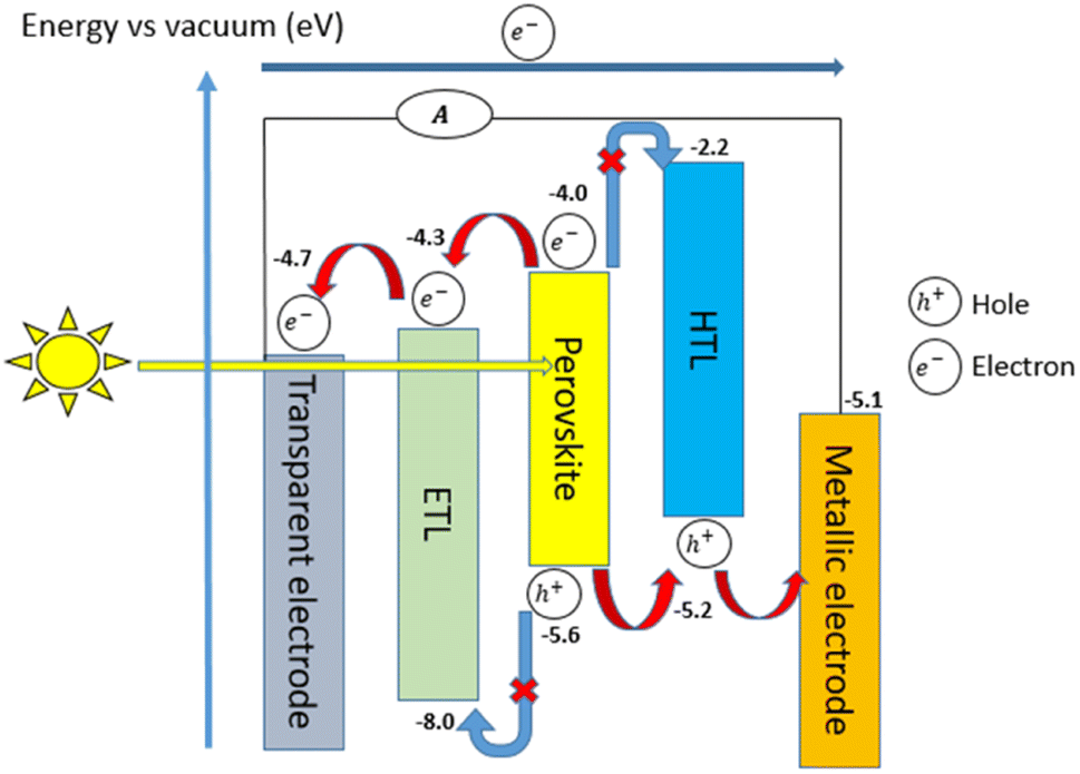
The working principle of a general PSC is described in Fig. 6, where each layer (Fig. 5) of the structure is carefully chosen to achieve optimal efficiency. This allows for the formation of different material energy levels, in addition to being thermodynamically compatible for a more robust device.
 |
| | Fig. 5 A generic structure of PSC for achieving the optimal efficiency based on the energy levels of materials from each layer. | |
 |
| | Fig. 6 A schematic of the operational principle of PSC. | |
Basically, PSCs work by initiating photon absorption in the perovskite layer, which originates from photons propagating through the electrode layer and the transparent glass (ITO/FTO coated glass). Decent absorption features can be achieved with a larger incident photon energy than that of the perovskite material, as this stimulates the excitation in the active layer of the perovskite. The important elements to consider in order to obtain optimal absorption depend on the HOMO (highest occupied molecular orbital) and LUMO (lowest unoccupied molecular orbital). When an electron moves from the HOMO (valence band edge of the PSC) to the LUMO (conduction band edge of the PSC), this sets the perovskite in an oxidized state and is then neutralized by electrons exiting the HOMO of the neighbouring HTL.
Due to the different work functions between the metal electrode and the transparent electrode, it creates an internal potential which leads the exciton to separate into holes and electrons.22 Both electrons and holes are then shifted from their current positions to the ETL and HTL, causing the holes to migrate to the metallic electrode, while the electrons migrate to the transparent electrode.22 Thus, the motion of the electron moving through the network between these two electrodes causes an electric current to be generated. It is important that the energy levels in each layer of the PSC are designed in such a way to avoid the recombination of excited charge carriers for the PSC to operate effectively under any conditions. Proper stratification to prevent charge carriers from mixing as they move in different directions through the cell can be achieved by introducing a LUMO energy level ETL that is below the perovskite energy level LUMO. Due to this, the electrons can move slightly further, allowing them to travel in the desired direction. In the meantime, the HOMO in HTL must exceed the HOMO in perovskite as this contributes to an efficient path for the hole to travel. In particular, each layer of cells is identical in this regard, and each layer requires a different HOMO or LUMO energy level for the charge carrier transport chain to function normally, as described in Fig. 5.22
3. PSC ETL characteristics
The ETL is an important layer in the PSC in generating high-efficiency performance, which plays a vital role as a photo-generated electron transporter. Nevertheless, the device behaviour and performance of PSC photovoltaics still experience challenges and limiting factors, such as carrier mobility, energy band alignment, defect morphology, trap states and related interface properties.23 Electrons are injected from the absorber layer, carried via ETL, and collected by the electrode in the ETL. Occasionally, an ETL is replaced with a composite photo electrode in order to improve the efficiency of the charge collection by reducing the amount of series resistance.24–26 In addition to this, a one-dimensional NRs ETL enables a solar cell to have a rapid charge transport. It has been discovered that managing the gaps that exist between the NRs and nanosheets can result in excellent pore filling, which is expedient for increasing both the fill factor (FF) and thereby the PCE of the material.27–34 Moreover, the concentrations of the fluid and the seed nanoparticle films play a role in determining the gap between the NRs. An ideal current–voltage behaviour is expected to be achieved as a result of the effective collection of charges. This is a method for growing the external quantum efficiency, also known as EQE, where it possibly provides the utmost efficiency while avoiding thermalization.
An ETL is undoubtedly necessary to satisfy the band alignment with the perovskite layer to be effective in charge conduction. This means that both its LUMO and HOMO have higher values than the perovskite active layer, as this is the most essential quality that an ETL must possess. In order for photons to simply pass through and be absorbed by the perovskite absorber, it is necessary for this material to have a high transmittance in the UV-Vis region. In addition, the excitation generated by light absorption across the perovskite layer is split prior to the ETL or HTL collection, and the excitons are said to dissociate either at the ETL/perovskite or perovskite/HTL interface sites, as reported by Savenije et al.35
3.1. Metal oxide as ETL materials in PSC
3.2. Titanium dioxide (TiO2)
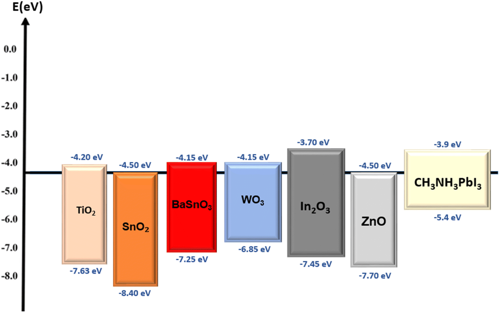
Generally, mesoporous TiO2 has been widely used as the ETL in PSC due to the general features mentioned earlier, yet the energy band is the main factor of the matter. Theoretically, TiO2 possesses a conduction band minimum of 4.2 eV and a valence band maximum of 7.63 eV (Fig. 7), which are ideal values in ensuring not only efficient electron transport from the perovskite layer, but also efficient hole-blocking capabilities at the perovskite interface.36 A large number of methods have been published to improve the performance of solar cells using TiO2 as the hole blocking layers, including spin-coating,37 spray pyrolysis,38,39 sol–gel,40 chemical bath deposition,41 and atomic layer deposition (ALD).42 The ability to enhance the PCE of the solar cells is one of the main advantages of these methods, along with reducing the higher recombination rate and decreased photocurrent, which negatively affects the solar cells performance. In addition, the first and unique mesoscopic solar cells based on a heterojunction between perovskite and TiO2 as the active layer are being developed,43 in which the PSC nanoparticles act as both light absorber and hole conductor, eliminating the need for an additional hole transport material. This method introduced simple solution-processed mesoscopic heterojunction solar cells-based TiO2, paving the way for low-cost and high-efficiency solar cell technology.
 |
| | Fig. 7 A summary of the energy levels of metal oxide materials as ETL and perovskite. | |
Besides the hole blocking layer, TiO2 is also widely used as ETL in PSC, although there are problems with the high recombination rate44 due to the limited electron mobility and surface defects in mesoporous TiO2 nanoparticles.45 In addition, the mesoporous TiO2 layer requires a high-temperature annealing process above 450 °C for complete crystallization, and the difficulty of achieving a uniform thickness with spin-coating technique, particularly for large-scale device production.46,47 On the other hand, PSC-based TiO2 as ETL also becomes unstable when exposed to UV light (sun or UV lamp) or when subjected to a forward bias for an extended period of time,48 as the charges generated by the perovskite layers are trapped at defects and impurities within the TiO2 layer. These TiO2 issues are challenges that researchers are actively working on to overcome the performance and stability of these devices. One way to resolve this problem is to introduce doping into TiO2 layers (Fig. 8), which has been shown to enhance the efficiency, Voc (open circuit voltage), Jsc (short-circuit current density), and fill factor, resulting in an increase in the absorption, electron mobility and reducing recombination rates.49
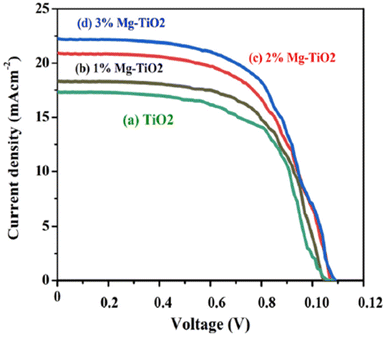 |
| | Fig. 8 J–V characteristics of PSC based on (a) bare TiO2, (b) 1% Mg-doped TiO2, (c) 2% Mg-doped TiO2, and (d) 3% Mg-doped TiO2. Reproduced with permission from ref. 49. Copyright 2021 Elsevier. | |
3.3. Tin oxide (SnO2)
Tin oxide, SnO2 is one of the most promising candidates of ETL for PSCs due to its superior optical and electrical properties,50 favourable band alignment with perovskite, and flexibility. The use of SnO2 as an ETL was initially demonstrated in dye-sensitized solar cells (DSSC), but it garnered little attention due to its relatively poor PCE when compared with TiO2-based DSSC.51 The preliminary investigations on the effects of SnO2 on PSCs were carried out almost simultaneously by several research groups, including Dai et al.52 and W. Ke et al.,53 who reported efficiencies of 10.18% and 17.21%, respectively. On the other hand, Hagfeldt et al.54 developed a combination of spin-coating and chemical bath post-treatment for PSC-based SnO2 in 2016, which achieved an efficiency of 20.7%, showing that the simple solution-processed tin oxide offers advantages in terms of scalability and cost effectiveness. Furthermore, in 2017, You et al. achieved the highest efficiency ever recorded in the planar PSC with an efficiency of 21.6% by using a two-step method to precisely control the PbI2 content because the excessive amount of PbI2 leads to significant hysteresis and poor stability. This method, which provides the novel design with specific optimization techniques, can lead to a power conversion of more than 21%.55
However, there are still issues related to the limited electron mobility of SnO2 as an ETL in PSC, which relates to the ability of electrons to move through the material and participate in efficient charge transport processes. To address this issue, researchers have explored various strategies to enhance the electron mobility of SnO-based ETL. These include surface engineering techniques56 and doping with other materials,57 as shown in Fig. 9(a) and (b), respectively, where the roughness of the PSC images deposited on nickel doped-SnO2 is smoother than on bare SnO2, while the surface morphology by SEM for nickel-doped SnO2 is greater than undoped SnO2, as illustrated in Fig. 9(c) and (d), respectively. These results are achieved through a low-temperature fabrication process with different nickel doping concentrations on SnO2-ETL, affecting the morphology and structure of the features. This result proves that the low-temperature process and doping implied in the fabrication of Ni-doped SnO2 ETL enables compatibility with flexible substrates, and simplifies the fabrication process of PSCs.
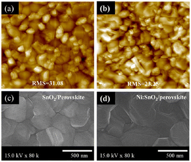 |
| | Fig. 9 Material images of (a) AFM for bare SnO2, (b) AFM for Ni-doped SnO2, (c) SEM for bare SnO2, and (d) SEM for Ni-doped SnO2. Reproduced with permission from ref. 57. Copyright 2022 American Chemical Society. | |
3.4. Barium stannate (BaSnO3)
Another reliable metal oxide material as an ETL for PSCs is barium stannate, BaSnO3 (BSO), in which the oxygen vacancies in BSO are naturally formed as an n-type semiconductor with a wide band gap of 3.1 eV (Fig. 7), and high electron mobility compared to other particles with suitable energy levels.58 Due to its unique properties and versatility, BaSnO3 is widely used in various applications, such as photocatalytic activity, sensors, gas sensing, dielectric and infrared luminescence.59–63 In addition, La-doped BSO single crystals and epitaxial thin films exhibit mobility values of about 320 cm2 V−1 s−1 and 70 cm2 V−1 s−1, respectively, which are unprecedentedly high.64 Due to these advantages, BSO has demonstrated utility in dye-sensitized solar cells,65,66 where it has shown promising results leading to improved device performance and increased energy conversion efficiency. In 2015, Zhu et al. compared the performance of the synthesis of mesoporous BSO (mp-BSO) with the conventional mesoporous TiO2 (mp-TiO2) as ETLs in PSCs. As a result, it has been discovered that mp-BSO offers the highest PCE with 12.3%, and has better contact with MAPbI3 by developing the crystals with greater cohesion. The mp-BSO device was found to have comparable performance to the mp-TiO2, but still had certain issues. For example, under high bias conditions, the mp-BSO possesses a faster charge recombination rate.67
To solve this problem, Zhu et al. fabricated novel mesoporous BaSnO3 ETL using solvent engineering technology in 2017 by doping with lanthanum (Fig. 10) and achieved the highest PCE of 15.1%, along with the highest produced Jsc of 19.1 mA cm−2.68 To date, various morphologies of BaSnO3 (such as NRs, nanoparticles and mesoporous) could be achieved by controlling the synthesis condition, as reported in a study from 2022,69 which investigated the morphology of brookite TiO2 and BaSnO3 as ETL. This finding reinforces the notion that the morphology design of materials can improve the electron properties of the layers, leading to higher efficiency and stability of the photovoltaic devices.
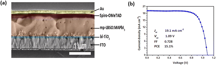 |
| | Fig. 10 (a) A cross-sectional view of SEM images from La-doped BSO in PSC. (b) J–V curves of La-doped BSO in PSC under AM 1.5 illumination. Reproduced with permission from ref. 68. Copyright 2017 Royal Society of Chemistry. | |
3.5. Tungsten oxide (WO3)
Tungsten oxide (WO3) is an n-type, wide-bandgap and low-oxygen semiconductor material that has received considerable attention in recent years, with an electrical band gap of 2.6 eV to 3.6 eV (Fig. 7).70–73 Due to its high specific surface area and high surface permeability, nanostructured WO3 is an excellent material for a wide range of applications. This material is a strong contender for use in optical and electrical applications74,75 due to its high melting temperature, photo-electrochromic properties, robustness and mechanical properties. In 2014, researchers made the first attempt to use WO3 and TiO2 as the core–shell electron transporting material in PSC, in which the novel structure of the WO3–TiO2 core–shell enhanced the electron extraction and transport capabilities.32
Thereafter, in 2015, K. Wang et al. investigated the use of a low-temperature, solution-processed amorphous WO3 thin film as ETL in PSCs in comparison to the conventional TiO2 ETL, resulting in higher electrical conductivity and comparable photoelectric conversion efficiency with an average of 8.99% efficiency.76 However, it also shows a lower open-circuit voltage and identifies inherent charge recombination as a limitation. Subsequently, Alexandre et al.77 in 2017 proposed the printable WO3 ETL as an alternative to TiO2 in PSC, and found that up to 9.5% PCE can be achieved with spin-coated or inkjet-printed WO3 compared to 15% for TiO2 reference. The advantage of WO3 in this experiment compared to TiO2 is that it allows a low-temperature process to be performed under ambient conditions, although they are more sensitive to ambient humidity when illuminated, resulting in a rapid drop in photocurrent.77 Furthermore, W-doped TiO2 has been proposed as an ETL for PSC,78 which uses a low-temperature solution-based method and shows an excellent performance of optimized PCE with 18.85% (Fig. 11), improving the carrier velocity and charge collection, JSC, and fill factor (FF) of the PSC. This research study suggests a promising approach for fabricating high-performance PSCs with tungsten-doped TiO2 materials.
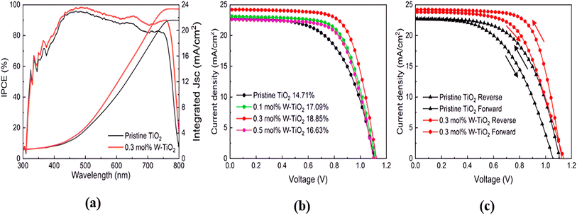 |
| | Fig. 11 (a) IPCE curves of pristine TiO2 and 0.3% mol W-doped TiO2. (b) IV curve of PSC with different W concentrations. (c) Reverse and forward direction of the IV curve. Reproduced with permission from ref. 78. Copyright 2021 Elsevier. | |
3.6. Indium oxide (In2O3)
Indium oxide (In2O3) is another promising n-type semiconductor material, with a wide band gap of 3.75 eV (Fig. 7), possessing a high mobility of 20 cm2 V−1 s−1, and excellent thermal stability with good transparency properties.79–81 These properties allow In2O3 to be an attractive and suitable candidate for future optoelectronic applications. In 2017, Yoon et al. fabricated In2O3 ETL-based PSC and organic solar cells by solution-process, with In2O3 showing better photo-stability than TiO2-PSC owing to the larger band gap. PSC showed retentions of 74% and 46% compared to the initial values measured under 1 sun illumination for 4 h.82
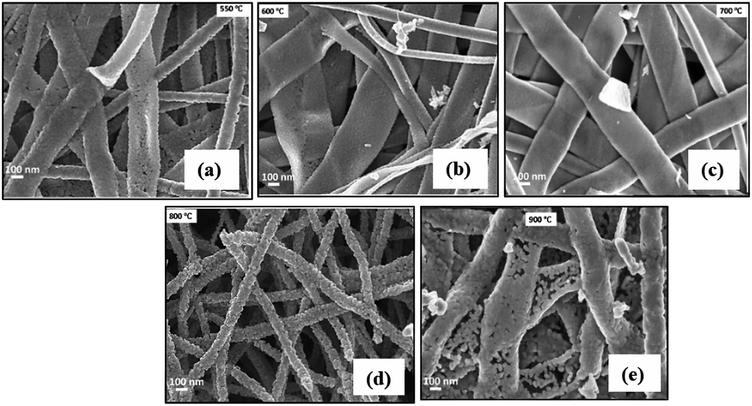
Other than photovoltaic application, In2O3 is also used in gas sensing,83 as reported by M. B. et al. in 2023, who developed a methane gas sensor-based mesoporous belt-like In2O3 (Fig. 12) from single-step electrospinning fabrication. The researchers studied how the annealing temperature affected the performance of the sensor by comparing the morphology, surface defects and structural behavior of the belt-like In2O3 to understand the trends in gas sensing. Among the annealing temperatures, the sensor annealed at 550 °C showed the best sensing capabilities with a response of 1.1 to 90 ppm of methane at a lower operating temperature of 100 °C, and had the best response and recovery times of 36 and 44 seconds, respectively. The unique mesoporous structure of the In2O3 materials contributed to their enhanced capabilities by providing numerous active sites for gas interaction. The findings provide insights into optimizing the sensor's design and fabrication parameters to enhance its sensitivity, selectivity and overall performance in detecting methane gas with implications for multiple areas, including industrial safety and power generation.
 |
| | Fig. 12 FE-SEM images of the In2O3 belt-like products annealed at (a) 550 °C, (b) 600 °C, (c) 700 °C, (d) 800 °C, and (e) 900 °C. Reproduced with permission from ref. 83. Copyright 2022 Elsevier. | |
3.7. Zinc oxide (ZnO)
Solar cell applications have extensively explored the utilization of ZnO materials owing to their exceptional stability, high electrical conductivity,84 elevated electron affinity, and remarkable electron mobility. Within the realm of binary compound semiconductors, ZnO stands as a prominent member classified under the II–VI category. It is noteworthy that ZnO materials do not exhibit significant absorption of visible light, instead manifesting as wide-bandgap semiconductors processing a bandgap range of 3.1 to 3.3 eV (Fig. 7). However, by combining ZnO with materials featuring smaller energy gaps, such as dye sensitizers and semiconductors with narrower band gap, it becomes feasible to shift the light absorption capabilities of ZnO into the visible range, thus enhancing its suitability for solar cell applications. As previously reported, the high electron mobility of ZnO ranges from 205 to 300 cm2 V−1 s−1 for bulk,85,86 and even reaches an impressive value of 1000 cm2 V−1 s−1 for ZnO NRs. This exceptional electron mobility renders ZnO a highly attractive material for utilization in solar cell applications, particularly when compared to the electron mobility values commonly used in TiO2, which typically range at around 0.14 cm2 V−1 s−1. The significantly higher electron mobility values associated with ZnO underline its favourable characteristics for efficient charge transport in solar cells.
Table 1 provides a comprehensive overview of the basic properties of ZnO, a chemical compound characterized by a molar mass of 81.408 g mol−1, and presents as a white solid with odourless properties. ZnO exhibits a density of approximately 5.606 g cm−3 and possesses a relatively high melting point of 1975 °C, at which point it undergoes decomposition, breaking down into its constituent elements, zinc (Zn) and oxygen (O). Conversely, the boiling point of ZnO is 2360 °C, indicating the temperature at which it transitions from a liquid to a gaseous state. ZnO showcases limited solubility in water, as evidenced by its solubility of approximately 0.16 mg per 100 ml of water at a temperature of 30 °C. This signifies that only a small quantity of ZnO dissolves in water under these particular conditions. One notable property of ZnO is its band gap, which denotes the energy difference existing between the valence band and the conduction band within the electronic structure of the material. In the case of ZnO, the band gap is approximately 3.3 eV, and it possesses a “direct” nature. This signifies that during transitions between the valence and conduction bands, both the momentum and energy of an electron can be conserved.87
Table 1 Basic properties of ZnO
| Properties |
| Molecular formula |
ZnO |
| Molar mass (g mol−1) |
81.408 |
| Appearance |
White solid |
| Odour |
Odourless |
| Density (g cm−3) |
5.606 |
| Melting point (°C) |
1975 (decomposes) |
| Boiling point (°C) |
2360 |
| Solubility in water |
0.16 mg/100 Ml (30 °C) |
| Band gap (eV) |
3.3 (direct) |
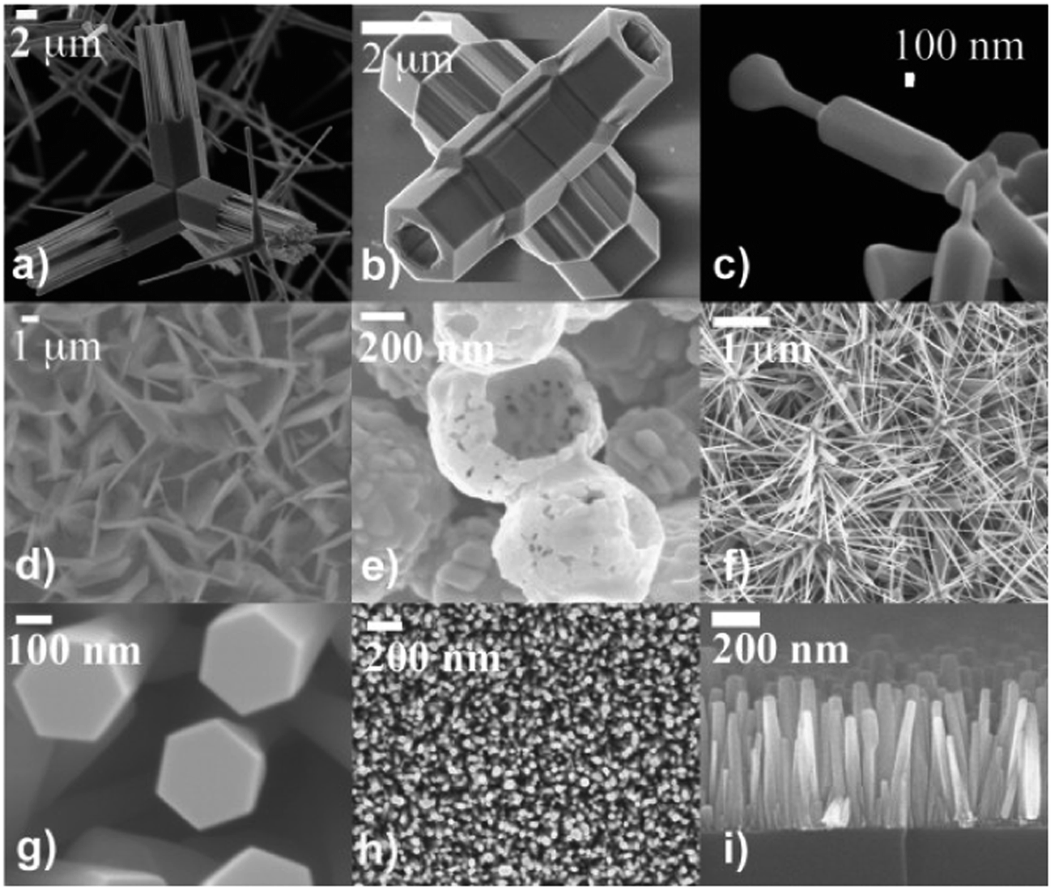
3.7.1. ZnO nanostructures. Nanorods, nanoflowers, nanowires, nanospheres, nanotubes, nanocrystals, and 3D nanostructures encompass the diverse range of ZnO nanomorphologies, as depicted in Fig. 13. The exceptional properties exhibited by ZnO have facilitated its extensive utilization across various fields, including solar cells. Notably, the incorporation of ZnO with different nanostructures leads to performances in PSCs, mainly due to the significant influence of the material structure on the PCE of PSCs. The presence of grain boundaries in the architecture of ZnO nanoparticles leads to numerous electron-capture events, and thereby hinders electron transfer.88–90
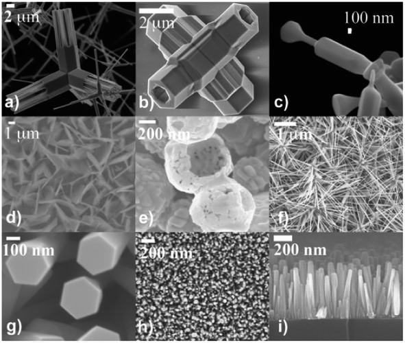 |
| | Fig. 13 Various ZnO morphologies from SEM images of the ZnO nanostructures: (a) and (b) tetrapod structures, (c) variable diameter structures, (d) nanosheets, (e) nanoshells, (f) multipods, (g)–(i) nanorods. Reproduced with permission from ref. 94. Copyright 2010 Elsevier. | |
In particular, Zheng et al.91 demonstrated that ZnO nanoparticles prepared by the spin coating method led to diminished PCE. This decline was attributed to the formation of pinhole surfaces, which generated defective interfaces and resulted in the loss of charge carriers. In contrast, one-dimensional nanostructured ZnO, such as NRs, exhibit significantly enhanced performance when compared to ZnO nanoparticles. This superiority primarily stems from the presence of one-dimensional single-crystal structures in ZnO NRs, facilitating direct electron pathways for electronic transport within PSC.92 Moreover, Mustaffa et al. discussed the concept of piezoelectric nanogenerators-based ZnO NRs in 2022, and have demonstrated their excellent performance due to their unique characteristics, such as a wide bandgap semiconductor energy and the ability to form ordered and uniform structures.93 Thus, these NRs well-defined pathways enable the observation of improved results in terms of electron transport and overall device performance.
4. Fabrication techniques in ZnO growth process
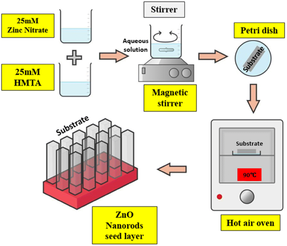
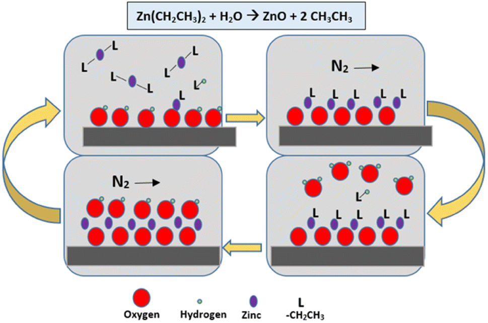
4.1. Hydrothermal
The hydrothermal fabrication method (Fig. 14) has garnered significant attention from researchers due to its inherent advantages: simplicity of equipment, cost-effectiveness, gentle preparation conditions, and an environmentally friendly approach.95 S. Mohan et al.96 conducted a study to explore the impact of reaction parameters on the structure of ZnO nanoparticles and their optical properties. They placed emphasis on the hydrothermal reaction conditions, varying the duration from 1 to 5 hours and the temperature from 100 °C to 150 °C. To analyse the influence of pH on nanomaterial development,97–101 a pH level of 12 was maintained. The researchers observed that the hydrothermal synthesis resulted in diverse nanostructures under different reaction parameters. Specifically, nanoflowers, NRs, and nanospheres were formed at temperatures of 100–120 °C for 2 hours, 120 °C for 1, 3, and 5 hours, and 150 °C for 2 hours, respectively.102 Additionally, the study concluded that nanoflowers and NRs exhibited superior photoluminescence, ultraviolet (UV) absorption, and an optimal bandgap.103,104 NRs, in particular, demonstrated enhanced heat stability compared to nanoflowers. Hence, it can be inferred that the hydrothermal approach enables the modification of nanomaterial structures in terms of size and shape. The duration of the reaction, temperature, and concentration of the reacting liquids are the primary factors determining the morphology of ZnO nanoparticles.
 |
| | Fig. 14 A schematic diagram of the ZnO NRs hydrothermal process. | |
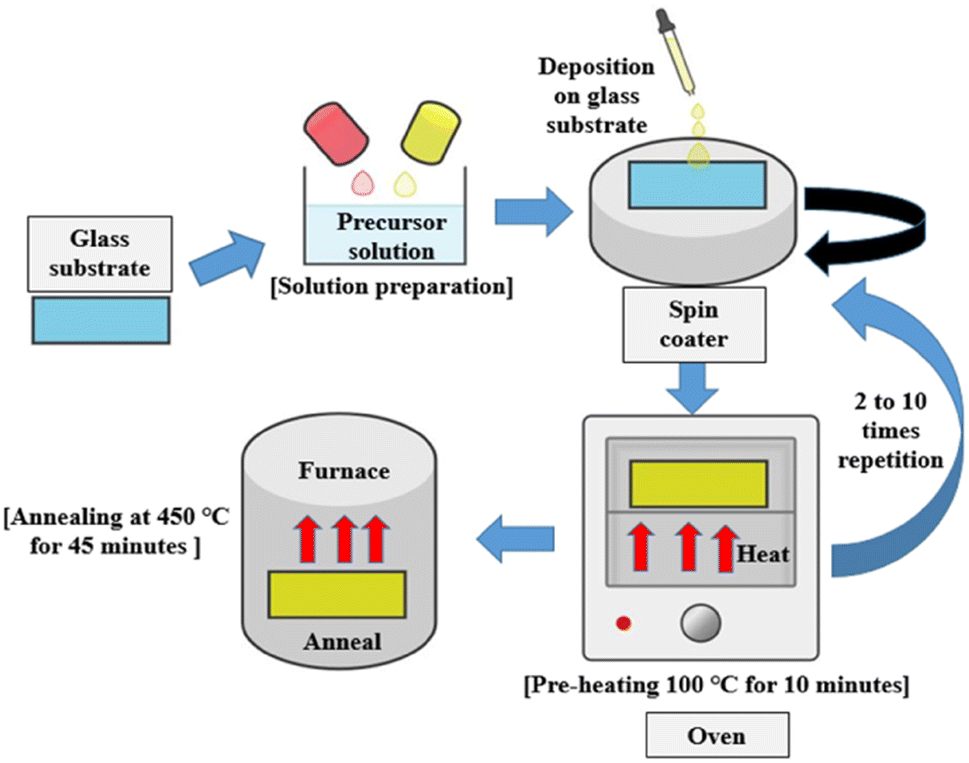
4.2. Sol–gel spin coating
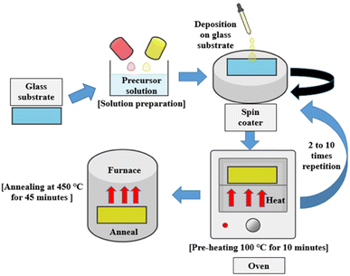
The sol–gel process, using spin-coating techniques as illustrated in Fig. 15, is highly attractive and widely used due to its straightforward nature, flexibility, and ease of doping. Moreover, it presents the opportunity to produce large-scale coatings at an affordable cost.105 In their study, Mursal et al.105 used sol–gel spin coating techniques to fabricate ZnO thin films. They investigated the influence of the annealing temperature on the optical properties, such as transparency, absorbance, and bandgap. The results revealed a notable correlation between the annealing temperature and the properties of the ZnO thin films. Notably, the optical bandgap of the ZnO films decreased as the annealing temperature increased. Additionally, the optical absorption coefficient of the ZnO films was found to be affected by the annealing temperature.
 |
| | Fig. 15 Sol–gel spin coating in the ZnO growth process. | |
In another study, M. A. Shafi et al.106 produced ZnO thin films for CZTS-based solar cells by varying the number cycles of spin coats to obtain different thicknesses of ZnO thin films on FTO substrates. A ZnO layer was formed after 8 and 10 cycles, and exhibited excellent surface density, crystallinity, roughness, and absence of pinholes with the observed bandgap ranging between 3.24 and 3.29 eV. Consequently, it can be inferred that both annealing temperature and rotation cycle significantly impact changes in the bandgap and structure of the solar cells.
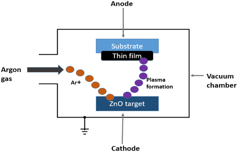
4.3. Sputtering
Magnetron sputtering (Fig. 16) is a highly suitable technology for the physical vapour deposition process, and enables the deposition of uniform ZnO layers over large areas at room temperature. It has been reported that magnetron-sputtered ZnO films significantly reduce the presence of hydroxyl groups on the film surface, positioning them as promising ETL for PSCs, as mentioned previously.107,108 H. Niu et al.109 used magnetron sputtering to produce high-quality ZnO films as efficient ETLs for PSC in 2021, and formed a ZnO/SnO2 bilayer structure by spin-coating a thin layer of colloidal SnO2 onto the ZnO underlayer. The bilayer ZnO/SnO2 ETL showed an impressive efficiency of 15.82%, surpassing 13.04% PCE achieved by the ZnO-based device. This study provides evidence that bilayer magnetron sputtering significantly improves PCE by facilitating good energy alignment in the cascade and efficient electron extraction at the ETL/perovskite interface. Thus, the bilayer ZnO/SnO2 ETL achieved a significantly higher efficiency of 15.82% compared to the PCE of the ZnO-based device of 13.04%, underscoring the potential of magnetron-sputtered bilayers for substantial PCE improvements.
 |
| | Fig. 16 A schematic of the ZnO RF magnetron sputtering system. | |
4.4. Atomic layer deposition
Atomic layer deposition, often known as ALD (Fig. 17) is a vapour phase thin film deposition process that is performed at low substrate temperatures, allowing for the uniform deposition of thin films. This scalable method is particularly attractive for industrial applications due to its suitability for large substrates. R. Pietruszka et al.110 explored the concept of utilizing ALD and hydrothermal processes to fabricate solar cell components (Zn/Si heterojunction solar cell), presenting greener and cost-effective alternatives that eliminate the need for extreme heat or potentially harmful chemicals. The textured structures achieved a maximum efficiency of 14%, while the planar structures reached 10%. In 2017, Shibin et al.111 used ALD to deposit Al2O3 monolayers on hydrothermally synthesized ZnO NRs to passivate interface defects. The PSC based on annealed ZnO-NRs passivated with ALD-Al2O3 demonstrated a maximum PCE of 16.08% and an average PCE of 15.08%.111 Therefore, the ALD of monolayers presents a novel technique for defect passivation in PSC, and it is worth noting that the different fabrication methods employed for ZnO NRs arrays can affect the performance of the PSC.
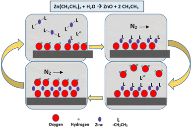 |
| | Fig. 17 A schematic illustration of ZnO atomic layer deposition synthesis. | |
5. Influences of dopants on ZnO as ETL in PSC
The introduction of impurities, also known as dopants, into semiconductor materials is defined as doping engineering. This allows the properties of the semiconductor to be modified to passivate defects in the bulk and at the interface, and improve bandgap alignment for enhanced charge carrier mechanism. Doping engineering involves incorporating specific elements of atoms into the semiconductor crystal lattice, thereby influencing the behavior of charge carriers (electrons or holes) in the semiconductor material and subsequently the performance of the solar cell device. Several authors have developed more sophisticated methods to enhance the electronic characteristics of ZnO-based ETL in PSCs through doping. Doping is typically employed to improve free charges and conductivity in solar cells, where it can drastically alter the structure of ZnO.112 As shown in Fig. 18, doping of ZnO can be achieved by exchanging either the Zn2+ cation or the O2− anion, where metals typically serve as cationic dopants and non-metals act as anionic dopants. Substituting Zn2+ with another cation can transform the structure of the conduction band (CB), while replacing the O2− anion with a different anion alters the valence band (VB) energy.113 In addition, numerous studies have demonstrated the effectiveness of ZnO doping for PSC applications, utilizing various dopant materials including metals (alkali metals, metalloids, transition metals), non-metals (halogens), and lanthanides (rare earth elements) in the ETL of solar cells.
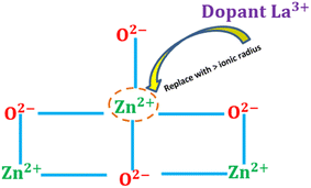 |
| | Fig. 18 A schematic image of the ZnO2+ cation substitution or passivation in the doping engineering process with lanthanum as an addictive dopant. | |
On the other hand, doping of ZnO as an ETL in PSCs can be understood in the context of Fick's law of diffusion, a fundamental principle that describes the movement of substances within materials, as explained in eqn (1) (Section 2) of this paper. Fick's law provides valuable insights into the movement of charge carriers, especially electrons, within the ZnO ETL of PSCs. According to eqn (1), Fick's law establishes a mathematical relationship between the flux (J), representing the rate of diffusion, and the concentration gradient (dn/dx) of the diffusing substance. In the context of PSCs, this gradient arises between electron-rich regions (n-type ZnO) and regions with fewer electrons (p-type perovskite or other layers), driving electron diffusion through the ETL. When dopants are introduced into the ZnO ETL, they significantly affect the diffusion properties, particularly the diffusion coefficient De, which measures the electron mobility. Doping increases the electron mobility and accelerates electron diffusion, resulting in higher De values and faster electron transport. Furthermore, dopants reduce the trapping and recombination centers within the ZnO ETL, enhancing the electron diffusion efficiency by preventing temporary electron capture in traps. Dopants can also align energy levels within the ETL, reducing energy barriers and allowing for more efficient electron diffusion. The overall goal of doping engineering is to optimize the electron diffusion efficiency within the ETL. This optimization leads to improved charge extraction and collection, minimizes losses due to recombination, and ultimately increases the overall efficiency of PSCs. In summary, Fick's law provides a fundamental framework for understanding how dopants in the ZnO ETL influence the charge carrier diffusion, a critical factor for improving the PSC performance.
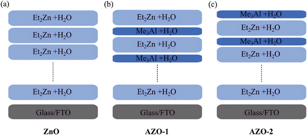
5.1. Aluminium-doped ZnO (ZnO:Al)
Both aluminium (Al) and zinc (Zn) are abundant, cost-effective, and non-toxic elements with ample availability. Doping with Al offers multiple benefits, including enhancing the stability of the ZnO/perovskite interface114 by modifying the fundamental properties of ZnO,115 but also significantly improves the carrier concentration and electron mobility of the material performance, as discussed in Section 5 regarding diffusion theory.116 In 2014, Mahmood et al. revealed that the PCE of PSC with AZO films deposited via electro spraying rises from 10.8% to 12.0%.117 The authors were able to achieve a high efficiency of 12% in PSC by precisely controlling the surface morphology of ZnO and Al-doped ZnO thin films through electrostatic spraying. Thereafter, A. Baltakesmez et al. presented the use of an inverted hybrid perovskite solar cell with an Al-doped ZnO substrate and anode electrode. The researchers found that AZO substrates prepared using RF magnetron sputtering with optimal growth parameters have similar electrical and optical properties to commercial indium tin oxide (ITO), with the PCE at approximately 10%, which is close to the PCE of around 13% for the cell based on the ITO substrate under one-sun illumination.118 Later in 2022, Joanna et al. reported the potential of atomic layer engineering techniques (Fig. 19) to improve the performance and stability of PSC through the precise control of Al-doped ZnO thin films. The authors demonstrate that by tailoring the properties of AZO films, such as optimizing their conductivity, transparency, and interface characteristics, the efficiency and long-term stability of PSC can be significantly improved.119 In the context of gas sensing for H2S detection, the gas sensing performance of the Al-doped ZnO thin films exceeded that of undoped ZnO films. This increase in performance is primarily due to the introduction of p-type conductivity and the consequent expansion of the films' surface area.120
 |
| | Fig. 19 A schematic representation of the growth process of ZnO and AZO films by ALD. This figure has been reproduced from ref. 119 with permission from Wiley, copyright 2022. | |
5.2. Silver-doped ZnO (ZnO:Ag)
Silver (Ag) dopants are of particular interest because of their characteristic surface plasmon resonance (SPR) effect, high surface area, and stable colloidal solution in water or organic solvents.121 In 2013, Ozlem et al. reported the influence of the silver content on the structural and optical properties of the resulting ZnO nanoparticles by fabricating silver-doped ZnO (Ag:ZnO) using precipitation method.122 It was revealed that the excessive amount of Ag led to a decrease in photocatalytic activity, and choosing the optimal amount of silver dopant is important to achieve the maximum photocatalytic performance. Another study123 investigated the impact of reduced graphene oxide (rGO) sheets on the enhancement of PCE in PSC using nickel (Ni)-doped ZnO and silver (Ag)-doped ZnO as ETL. The results indicated that Ag doping at 5 wt% played a beneficial role in separating charge carriers and reducing the recombination rate by introducing defect states in ZnO-based PSC. Besides that, according to the findings of G. Bagha et al., shallow trap generation by Ag doping contributes to charge extraction. As a result, a rGO/Ag-doped ZnO bilayer ETL was created as a new approach to fabricate stable planar PSCs with low charge recombination rate and good performance, as discussed in Section 5 regarding diffusion theory. After the addition of rGO sheets and Ag doping, Voc increases and causes the carrier recombination to decrease, thus leading to an increase in PCE by 30% from 7.40% to 11.03%, as shown in Fig. 20.124 Therefore, Ag is not a dopant in its own right; in order to obtain a greater PCE, the Ag-doped substance must be modified.
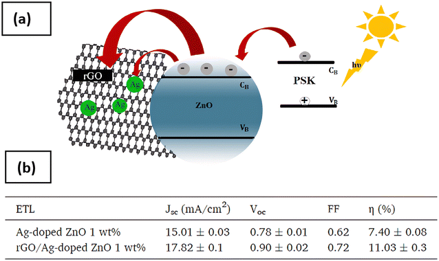 |
| | Fig. 20 (a) The functionality of rGO/Ag-doped (1 wt%) bilayer ETL of PSC ZnO. (b) J–V characteristics of Ag-doped and rGO/Ag-doped ZnO (1 wt%). Reproduced with permission from ref. 124. Copyright 2021 Elsevier. | |
5.3. Iodine-doped ZnO (ZnO:I)
Iodine is a chemical element with the symbol I and belongs to the halogen group of the periodic table, which is a lustrous, purplish-black solid at room temperature. It is highly reactive, classified as a non-metal known for its distinctive violet colour, and forms a vapour when in contact. In 2017, Zheng et al.125 fabricated one dimensional (1D) ZnO:I nanopillars ETL (Fig. 21) for PSC using a one-step spin coating process, and the PCE was boosted up to 18.24%, surpassing the previous highest efficiency achieved with 1D ETL-based PSC. It has been proven that the exceptional cell performance is due to the following properties of the low aspect ratio (LAR) ZnO:I nanopillars ETL with a refined flat surface. This research introduces a novel and efficient 1D ETL approach by incorporating alien element doping and controlling the crystal orientation growth, leading to the maximization of the PSC performance. However, there are only a few studies that have reported on iodine as a dopant in PSC because most of them are used in dye-sensitized solar cells that greatly improved the PCE.126–128 As dye-sensitized solar cells DSSCs have a longer research and development history compared to PSCs, iodine has been extensively studied and demonstrated as an effective dopant in DSSCs, showing improved charge transport and stability, as discussed in Section 5 regarding diffusion theory. Therefore, many studies focused on utilizing iodine in DSSCs rather than in PSC, where its efficacy was already established. In addition, the utilization of iodine-doped ZnO as ETL in PSC research has ceased since 2017. This is primarily due to a combination of factors including iodine migration and degradation, as well as challenges associated with iodine loss. Iodine poses a unique challenge to the stability of PSC, especially in the presence of metallic electrodes. When these PSCs are exposed to such electrodes, the electric field generated between them can initiate a process in which iodine ions are displaced. This can lead to the migration of I− ions, which ultimately leads to degradation of PSC performance.129 Besides that, iodine loss resulting from a range of factors such as moisture, oxygen, and light exposure, poses a substantial challenge in the pursuit of enhancing both the PCE and long-term durability of PSCs.130,131 Nevertheless, in the field of sensor technology, there has been a recent breakthrough involving the use of I-doped ZnO for detecting ethyl paraben (EP),132 where EP is commonly employed as a preservative in a wide range of personal care products, and the ability to detect it at low concentrations is of utmost importance for ensuring product quality and safety. This study identified an optimal level of iodine doping in ZnO that significantly increases the performance of the sensor and positions it as a promising material for EP detection. I-doped ZnO has also proven to be highly effective in detecting high-quality latent fingerprints on a variety of substrates, demonstrating its significant potential in forensic investigations.133
 |
| | Fig. 21 A schematic illustration of the PSC configuration, in which a dense and homogeneous perovskite cap layer completely covers the ZnO:I nanopillars. Reproduced with permission from ref. 125. Copyright 2017 Royal Society of Chemistry. | |
5.4. PbX2-doped ZnO (ZnO:PbX2)
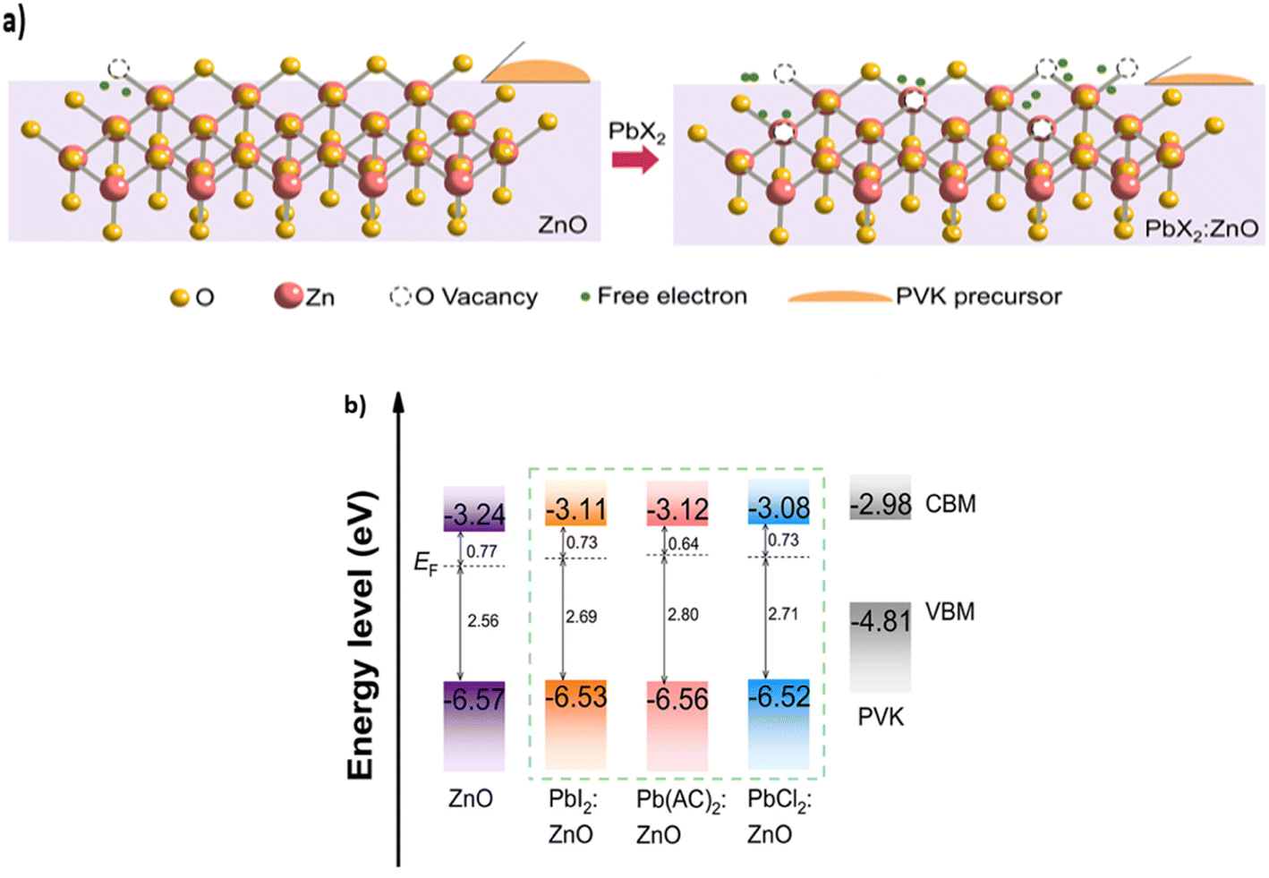
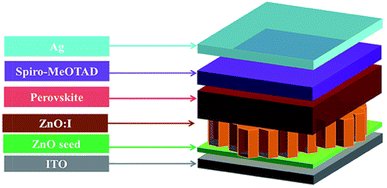
PbX2 compounds are ionic solids that exhibit solubility in water and polar solvents. These compounds possess high melting and boiling points, and demonstrate stability at elevated temperatures.134 In materials science, PbX2 compounds find diverse applications, particularly as precursors for the synthesis of perovskite materials utilized in solar cells.135 In the context of PSC, an innovative methodology involving the incorporation of PbX2 (X = I−, Cl−, and CH3COO−) compounds as dopants within ZnO layers has been reported by Wu et al., where the ZnO films were prepared using a sol–gel method. PbX2 (X = I, Cl, and CH3COO) was then incorporated into the ZnO films by adding the PbX2 precursor to the ZnO precursor solution under 200 °C annealing temperature. From the study, the efficiency of the all-inorganic perovskite solar cells is boosted from 17.64% to 20.04% with a fill factor of 84.14% and a highest reported open-circuit voltage (Voc) of 1.28 V among highly efficient all-inorganic PSCs. The PbX2 PSCs also exhibit enhanced stability, retaining above 97% of the initial PCE after 1000 hours and demonstrating improved photostability. The integration of PbX2 leads to increased density of oxygen vacancies (Fig. 22(a)), consequently leading to a higher electron concentration through n-type doping, with the Fermi levels becoming closer to the conduction band minimum (CBM), as shown in Fig. 22(b).136 A higher concentration of oxygen vacancies on the ZnO surface leads to an increase in the Fermi level through n-type doping, which in turn increases the wettability and facilitates the subsequent deposition of an advanced perovskite film on the surface. Besides that, it has been reported that using an ETL with a shallower energy level has increased the VOC, while establishing favorable conduction band alignments with the perovskite layer.137,138 Consequently, charge recombination was effectively suppressed and charge extraction became more efficient, demonstrating the significant improvement in both VOC and FF, as discussed in Section 5 regarding diffusion theory. Thus, this significant improvement not only represents a new milestone in the field of purely inorganic PSCs, but also represents a groundbreaking advancement in photovoltaic technology. It expands the applicability of PSCs to a wider range of critical applications that require high-voltage outputs, thereby enhancing their versatility and utility in the field of renewable energy.
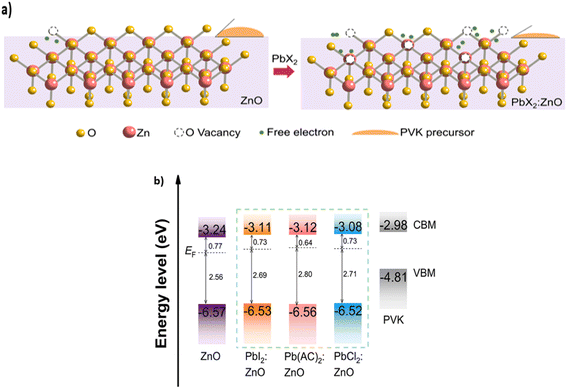 |
| | Fig. 22 (a) Energy level alignment of ETLs and the perovskite layer. (b) Visualization of the impact of the enhanced oxygen vacancy in PbX2:ZnO. This figure has been reproduced from ref. 136 with permission from Wiley, copyright 2022. | |
6. Recent advances and future perspective
6.1. Lanthanum-doped ZnO (ZnO:La)
Lanthanum (La), a cationic rare earth metal oxide in powder form, exhibits a wide range of useful industrial qualities, with the particle size of the powder being in the nanoscale of 1–100 nm. In electrochemistry, lanthanum oxides are used to produce organic catalysts. It is used as an electrode, and the burning rate of propellants can also be increased by lanthanum oxide.139,140 Furthermore, previous research suggested that adding a small amount of La to doped ZnO can significantly improve its photocatalytic properties by: (i) enhancing charge separation; (ii) increasing surface area and active sites; (iii) shifting in band-edge positions; and (iv) reducing charge carrier recombination,141–143 as discussed in Section 5 regarding diffusion theory. In a study by C. Chamanzadech et al.,144 La-doped ZnO were synthesized using the hydrothermal method. Varying the concentration of La dopants resulted in a remarkable improvement of the PCE with a 63.6% increase compared to conventional DSSC utilizing TiO2 nanoparticles. On the other hand, the PCE increment of La-doped ZnO is almost 97% when compared to the pure ZnO. Synthesis of optical property measurements showed enhanced absorption, with the changes in the bandgap energy almost similar to the pure ZnO with 3.218 eV, showing higher absorbance coefficient and resulting in higher PCE. The photovoltaic performance data for DSSCs, such as improved PCE, current–voltage (I–V) curves, fill factor, short-circuit current (Jsc), and open-circuit voltage (Voc), demonstrated significant enhancements achieved through the use of La-doped ZnO NRs compared to conventional photoanodes. These comprehensive findings collectively underscore the promise of utilizing La-doped ZnO nanorods in enhancing the photovoltaic performance of DSSCs. Given the promising results observed in this study, particularly in the enhancement of solar cell performance through the use of ZnO nanorods doped with La, it has become intriguing to consider the application of these findings in the field of PSCs since the application of La-doped ZnO as an ETL in PSCs remains relatively unexplored. However, in the context of other solar cell types, the incorporation of La (frequently in conjunction with other elements) has exhibited notable enhancements in PCE, as outlined in Table 2. The utilization of La-doped ZnO extends beyond the realm of solar cell applications. It has found diverse applications, ranging from piezoelectric nano-generators to dye photodegradation, drug delivery systems, wastewater purification, and antibacterial activity, as comprehensively summarized in Table 3.
Table 2 Lanthanum as a dopant in solar cell applications
| Solar cell |
ETL |
Morphology |
Method |
PCE (%) |
Year |
Ref. |
| PSC |
La/BaSnO3 |
Bare surface nanocrystal |
Laser manufactured |
23.74 |
2022 |
145 |
| Planar PSC |
La/SSO |
Smooth crystal grain |
Low-temperature solution |
18.7 |
2021 |
146 |
| Cs2TiBr6-based PSC |
La/BaSnO3 |
— |
Numerical analysis by SCAPS 1D |
29.13 |
2021 |
147 |
| Dye-sensitized solar cell (DSSC) |
La/ZnO, Dy/La |
Nanorods |
Spin coating, hydrothermal |
6.22, 6.52 |
2021 |
144 |
| Inverted organic solar cell (IOSC) |
La/ZnO |
Nanospheres |
Sol–gel |
4.34 |
2020 |
148 |
| Planar PSC |
Al/La/SnO2 (co-doped) |
— |
Low-temperature solution |
19.13 |
2020 |
149 |
| Planar structure hybrid PSC |
La/SnO2 |
Hexagonal disc |
Low-temperature solution |
17.08 |
2019 |
150 |
| Dye-sensitized solar cell (DSSC) |
La/SrSnO3 |
Nanocoral |
Wet-chemical route |
4.7 |
2018 |
151 |
| PSC |
La/TiO2 |
Hexagonal disc |
Spray-pyrolysis |
17.2 |
2017 |
152 |
| Inverted organic solar cell (IOSC) |
La/TiO2 |
Small hole grain |
Sol–gel |
2.45 |
2017 |
153 |
| PSC |
La/BaSnO3 |
Nanobead |
Hydrothermal |
15.1 |
2017 |
68 |
Table 3 La-doped ZnO in other applications
| Application |
Method |
Morphology |
Advantages |
Year |
Ref. |
| UV photodetectors |
Spray technique |
Nanorods |
5% of La–ZnO layers excel in UV photodetection with a sensitivity of 5.07 |
2023 |
154 |
| Rhodamine B degradation |
Electrospinning-calcination |
Nanofibers |
La-doped ZnO catalyst more efficient than undoped ZnO in Rh B degradation |
2022 |
155 |
| Great potential in Rh B dye wastewater |
| Dye-photodegradation |
Electrospinning-calcination |
Nanofibers |
La-doped ZnO showed higher photocatalytic activity compare to undoped ZnO |
2019 |
156 |
| Successfully used in photodegradation of CR dye |
| Piezoelectric nano-generator |
Wet chemical route |
Nanorods |
The output of piezoelectric was enhanced by 4–5 times with 5% of La-doped ZnO |
2019 |
157 |
| High stability in sensor analysis with more than 4500 cycles |
| Antibacterial study |
Co-precipitation |
Nano-sphere |
Lanthanum doping concentration controls ZnO nanoparticle size, band gap, and photoluminescence |
2017 |
158 |
| Suitable for antibacterial activities as treatment for kidney stone and typhoid fever |
| Metasystox degradation |
Microwave assisted |
Nanorods |
La-doped ZnO completes metasystox mineralization faster than pure ZnO |
2014 |
159 |
| La-doped ZnO metasystox safe for plant growth |
6.2. Doping elements of ZnO-ETL in PSC and other doping elements in other solar cells
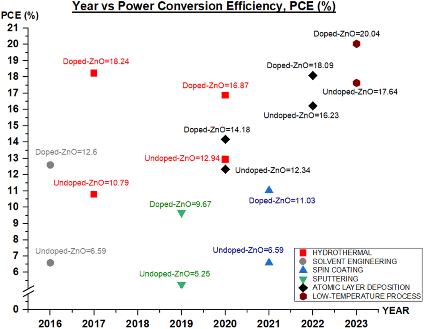
Doping typically leads to increased conductivity in ZnO, and this effect depends both on the electronegativity of the dopant element and the difference in radius between the dopant and zinc ion. Additionally, to address the instability of ZnO at high temperatures, doping with other elements has been employed to enhance its properties. In particular, ZnO elemental doping has shown promising results in improving the efficiency of PSCs through various fabrication methods, as depicted in Fig. 23 and detailed in Table 4. Doping is widely recognized as a crucial technique for enhancing solar cell performance, leading to its extensive application across different types of solar cells, as summarized in Table 5.
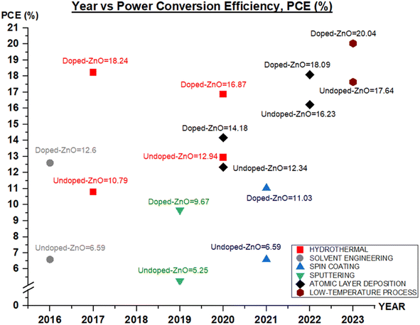 |
| | Fig. 23 Current status of PCE ETL with doped-ZnO and undoped-ZnO in PSC with different fabrication techniques in the last decade. | |
Table 4 A summary of ZnO doped in PSCs
| Solar cell |
ETL |
Nanostructure |
Dopant |
Ionic radius (Å) |
Method |
Year |
PCE (%) |
Ref. |
| PSC |
ZnO |
Amorphous |
Aluminium (Al) |
0.54 |
Sol–gel |
2023 |
7 |
160 |
| CsPb(I1−xBrx)3, PSC |
ZnO |
Pinhole-free |
PbX2, X = I, Cl, CH3COO |
1.19 |
Low-temperature process |
2022 |
20.04 |
136 |
| PSC |
ZnO |
— |
Aluminium (Al) |
0.54 |
Atomic layer deposition |
2022 |
18.09 |
119 |
| Planar PSC |
ZnO |
Nanospheres |
Graphene oxide silver-doped bilayer, *rGO/Ag-doped |
1.26 |
Modified hummers, combustion, spin-coating |
2021 |
11.03 |
124 |
| PSC |
ZnO |
Nanorods |
Nitrogen (N), graphene (G), N/G-doped |
N = 1 |
Hydrothermal |
2020 |
16.87 |
161 |
| Flexible PSC |
ZnO |
Nanowires |
Aluminium (Al) |
0.54 |
Atomic layer deposition |
2020 |
14.18 |
162 |
| Planar PSC |
ZnO |
Amorphous |
Gallium (Ga) |
0.62 |
Graded sputtering |
2019 |
9.67 |
163 |
| PSC |
ZnO |
Nanopillars |
Iodine (I) |
2.2 |
Hydrothermal |
2017 |
18.24 |
125 |
| PSC |
ZnO |
Hexagonal disc |
Aluminium (Al) |
0.54 |
Solvent engineering |
2016 |
12.6 |
115 |
Table 5 A summary of other doping elements in other solar cells
| Solar cell |
ETL |
Nanostructure |
Dopant |
Ionic radius (Å) |
Method |
Year |
PCE (%) |
Ref. |
| Carbon-based PSC |
TiO2 |
Pin-hole free |
Lithium (Li) |
0.76 |
One-step |
2023 |
8.09 |
164 |
| PSC |
SnO2 |
Nanocrystal |
Chlorine (Cl) |
1.81 |
Chemical bath deposition |
2023 |
25 |
165 |
| PSC |
TiO2 |
Porous |
Erbium (Er), neodymium (Nd) |
0.881, 0.995 |
Solid-state grinding |
2023 |
12.50 |
166 |
| PSC |
TiO2 |
Mesoporous |
Tin (Sn) |
0.71 |
Sol–gel |
2022 |
20.55 |
167 |
| PSC |
TiO2 |
Nanograins |
Nitrogen-based group (N) |
1 |
Sputtering, sol–gel |
2022 |
5.33 |
168 |
| Inorganic halide PSC |
TiO2 |
Nanorods |
Cesium (Cs) |
1 |
Hydrothermal |
2022 |
12.72 |
169 |
| Planar PSC |
SnO2 |
Nanoflowers |
Nickel (Ni) |
0.69 |
Low temperature solution |
2022 |
19.7 |
57 |
| Planar PSC |
SnO2 |
Right bipyramids |
Copper (Cu) |
0.73 |
Low-temperature, spin coating |
2022 |
21.35 |
170 |
| Heterojunction solar cell |
ZnO |
— |
Aluminium (Al) |
0.54 |
Sol–gel |
2022 |
8.984 |
171 |
| Pbs quantum dots solar cell |
ZnO |
Nanograins |
Magnesium (Mg) |
0.72 |
Hydrothermal, hot injection |
2021 |
9.46 |
172 |
| Inverted polymer solar cell |
ZnO |
— |
Indium (In) |
0.8 |
Solution-processed, sol–gel |
2021 |
5.99 |
173 |
| Inverted polymer solar cell |
ZnO |
Smooth grain |
Indium (In), gallium (Ga), IG/ZO |
In = 0.8, Ga = 0.62 |
Sol–gel spin coating |
2021 |
8.72 |
174 |
| Flexible PSC |
ZnO |
Nanorods |
Cobalt (Co) |
0.745 |
Hydrothermal |
2020 |
7 |
175 |
| Polymer solar cell |
ZnO |
Nanospheres |
Gold (Au) |
0.85 |
Seed-growth |
2020 |
8.801 |
176 |
| DSSC |
ZnO |
Branched network |
Manganese (Mn) |
0.46 |
Hydrothermal |
2020 |
4.20 |
177 |
| Quantum dot-sensitized solar cell (QDSSC) |
TiO2 |
Nanospheres |
Lanthanum (La) |
1.061 |
Co-precipitation |
2020 |
3.28 |
178 |
| DSSC |
ZnO |
Nanobead |
Copper (Cu) |
0.73 |
Hydrothermal |
2020 |
1.50 |
179 |
| Polymer solar cell |
ZnO |
— |
Cadmium (Cd) |
0.97 |
Solution-processed |
2020 |
14.7 |
180 |
| Inverted polymer solar cell |
ZnO |
— |
Gallium (Ga) |
0.62 |
Low-temperature sol–gel |
2019 |
7.7 |
181 |
| Organic solar cell |
ZnO |
— |
Lithium (Li), cesium (Ce), Li/Ce |
Li = 0.76, Cs = 1.67 |
Sol–gel |
2019 |
9.074 |
182 |
| PSC |
ZnO |
Nano-ginger |
Aluminium (Al) |
0.54 |
Low-temperature |
2019 |
7 |
183 |
| Organic solar cell |
ZnO |
Nanospheres |
Aluminium (Al) |
0.54 |
Sol–gel |
2019 |
3.24 |
184 |
| Inverted polymer solar cell |
ZnO |
— |
Aluminium (Al) |
0.54 |
Sol–gel |
2016 |
3.25 |
185 |
7. Discussion
In this review, we thoroughly discuss various materials of the ETL in PSCs and other emerging solar cell technologies. ZnO NRs have demonstrated superior features for the extraction and conduction of electrons, primarily due to their one-dimensional single-crystal structures, which facilitate efficient electronic transport in PSCs. Various fabrication techniques have been explored for the production of highly oriented ZnO NRs, where the hydrothermal synthesis method has appeared as the best method due to its simplicity, cost-effectiveness, mild conditions and environmental friendliness. Moreover, the ZnO NRs have exhibited remarkable thermal stability compared to other nanostructures during the hydrothermal process.
To enhance the functionality of ZnO as an ETL, doping engineering offers a viable approach to tuning the properties of the semiconductors. Apparently, doping involves the process of implanting certain elements into the crystal lattice, which offers the capability to modulate the energy band gap and improve the photocatalytic properties of ZnO, thereby increasing the PCE of solar cells. The physical and chemical properties of doped ZnO strongly depend on the choice of doping elements. A wide range of dopants on ZnO ETL PSCs, characterized by ionic radii closely resembling that of ZnO (0.74 Å), have been extensively studied as listed in Table 4, and their promising performance in terms of efficiency is shown in Fig. 24. This figure of merit highlights the importance of carefully selecting dopants for the ZnO ETL in PSCs, where the ionic radii of dopant ions and host Zn ions should be remarkably similar, allowing for nearly identical substitution within the ZnO vacancy. This process effectively involves the impurity (dopants) occupying the voids or interstices among the host Zn atoms, particularly within the ZnO vacancy sites. This criterion aims to maintain the structural integrity and stability of the ETL, which can significantly impact the overall PCE of the PSCs. Nevertheless, the use of lanthanum with 1.061 Å ionic radius as a dopant in ZnO for PSC has not yet been studied and its effectiveness has not yet been explored. Therefore, this paper proposes a novel approach for incorporating lanthanum into ZnO as an ETL in PSC. Due to the ionic interaction between Zn2+ and O2−, pure ZnO does not have a free carrier charge. However, if Zn2+ ions are replaced by La3+ ions in the ZnO matrix, this leads to an increase in the number of free electrons in the valence band. This could instigate the electrons in the valence band to require more energy to jump to the free states at the conduction band, as the lowest state of the conduction band is already occupied by electrons. This decreases the amount of energy required to excite the electron into the lowest energy empty band in the semiconductor, and therefore increases the number of electrons that have enough energy to cross this gap. Besides that, when Zn2+ replaces La3+ in the crystal lattice, the average ionic radius of the material may decrease because zinc has a smaller ionic radius than lanthanum.
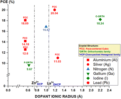 |
| | Fig. 24 Summary of impacted factors on PCE for various types of dopants in ZnO ETL-PSC. | |
Other than the ionic radius, other factors are crucial in assessing the compatibility of La-doped ZnO within the context of its application as a dopant, particularly in solar cell technologies. These impacted factors, including the crystal structure, valence band alignment and electronegativity, are compared with other dopants, as shown in Fig. 24 and Table 6. It is noteworthy that among the various dopants used, La bears a striking similarity to Zn due to their shared crystallographic lattice, where both ZnO and La belong to the hexagonal crystal family. This shared hexagonal symmetry promotes their compatibility as dopants within the host lattice. A matching crystal structure minimizes the lattice defects and strain, ensuring better crystalline quality and electrical properties. Furthermore, La can seamlessly integrate into the ZnO valence band with a +2 valence state. This similarity in valence states aligns their energy levels, facilitating charge transport and enhancing compatibility. This allows La to contribute charge carriers to the valence band, which is crucial for optimizing the electronic properties. Additionally, the +2 valence state of La makes it relatively easy to dissolve and incorporate into the ZnO lattice. The presence of La ions with a +2 charge helps maintain charge balance within the host material. This ease of dissolution promotes homogeneous distribution, preventing the formation of defects that could impair the structural integrity. Despite La having a lower electronegativity than oxygen, it does exhibit some degree of electronegativity compatibility with Zn. This modest electronegativity similarity between La and Zn can facilitate stable dopant–host interactions. As a result, it helps to minimize the charge imbalances and reduce electrostatic forces, which, in turn, contributes to the overall compatibility of La-doped ZnO.
Table 6 Impacted factors on PCE for various types of dopants in ZnO ETL-PSC
| Dopants |
Crystal structure |
Valence state |
Ionic radius (Å) |
Electronegativity |
PCE (%) |
| Zinc (Zn) |
HCP |
+2 |
0.74 |
1.65 |
— |
| Lanthanum (La) |
DHCP |
+2 |
1.061 |
1.10 |
— |
| Aluminium (Al) |
FCC |
+3 |
0.54 |
1.61 |
18.09 (ref. 119) |
| 14.18 (ref. 162) |
| 12.60 (ref. 115) |
| Silver (Ag) |
FCC |
+1 |
1.26 |
1.93 |
11.03 (ref. 124) |
| Nitrogen (N) |
NA |
−3 |
1 |
3.04 |
16.87 (ref. 161) |
| Gallium (Ga) |
F-ORTH |
+3 |
0.62 |
1.81 |
9.67 (ref. 163) |
| Iodine (I) |
C-ORTH |
−1 |
2.2 |
2.66 |
18.24 (ref. 125) |
| Lead (Pb) |
FCC |
+4 |
1.19 |
2.33 |
20.04 (ref. 136) |
8. Conclusion
The improved quality of ETL will lead to an effective PCE, and allow the cells to become genuinely revolutionary in PSCs technologies. In this paper, several types of metal oxide as electron transport materials were discussed, including TiO2, SnO3, BaSnO3, WO3, In2O3 and ZnO. Among these materials, ZnO with NRs morphology has demonstrated favourable performance as an ETL due to its direct electron pathway in solar cells. As part of this comprehensive review, we have discussed various fabrication techniques that have been prominently utilized over the past decade. These techniques span a spectrum of methods, including hydrothermal synthesis, solvent engineering, spin coating, sputtering, atomic layer deposition, and low-temperature processes. Hydrothermal synthesis has emerged as the preferred method compared to other syntheses for producing ZnO NRs owing to its cost-effectiveness, ease of implementation, low energy consumption, and minimal environmental impact. The prevailing issue of the Zn2+ defect vacancy is believed to be improved by adding doping elements into the ZnO ETL layer. To address this, we have explored the addition of various dopants into the ZnO ETL layer. Our findings demonstrate that the incorporation of these dopants not only mitigates Zn2+ defect vacancies, but also yields a multitude of benefits, including enhanced electron diffusion, improved stability of PSCs, optimized charge extraction and collection, reduction in losses due to recombination, and, ultimately, a substantial increase in the overall efficiency of PSCs. With careful selection and optimization of dopants, the resulting solar cells have the potential to increase the charge carrier conduction, reduce recombination and improve the energy level alignment with the perovskite layer. Lanthanum is a promising dopant derived from rare earth materials, and has shown significant improvement in the photocatalytic properties of solar cells. The compatibility of La with Zn in the crystal structure, valence state, and electronegativity significantly contributes to its effectiveness as a dopant, thereby establishing it as an indispensable component for improving the photocatalytic properties of solar cells and further developing the field of photovoltaics. Nevertheless, the rare earth material lanthanum is still not widely studied and explored as a dopant in ZnO ETL in PSC. Therefore, this review presents a new paradigm with a doping engineering approach as an alternative means for the fabrication of highly efficient ETL in PSC. While this assumption holds true for most practical scenarios, further investigations can be undertaken to explore and validate this approach.
Conflicts of interest
There are no conflicts to declare.
Acknowledgements
This work was supported by Universiti Teknikal Malaysia Melaka and Ministry of Education Malaysia under Grant FRGS/1/2020/TK0/UTEM/03/12.
References
- International Renewable Energy Agency, Net renewable capacity additions by technology, 2017–2023, https://www.iea.org/data-and-statistics/charts/net-renewable-capacity-additions-by-technology-2017-2023, accessed 12 April 2023.
- N. Shrivastav, J. Madan, R. Pandey and A. E. Shalan, RSC Adv., 2021, 11, 37366–37374 RSC.
- B. O'Regan and M. Grätzel, Nature, 1991, 353, 737–740 CrossRef.
- N. G. Park, Mater. Today, 2015, 18, 65–72 CrossRef CAS.
- A. M. Elseman, W. Sharmoukh, S. Sajid, P. Cui, J. Ji, S. Dou, D. Wei, H. Huang, W. Xi, L. Chu, Y. Li, B. Jiang and M. Li, Adv. Sci., 2018, 5, 1800568 CrossRef PubMed.
- T. H. Schloemer, J. A. Christians, J. M. Luther and A. Sellinger, Chem. Sci., 2019, 10, 1904–1935 RSC.
- J. Urieta-Mora, I. García-Benito, A. Molina-Ontoria and N. Martín, Chem. Soc. Rev., 2018, 47, 8541–8571 RSC.
- W. Zhang, Y. C. Wang, X. Li, C. Song, L. Wan, K. Usman and J. Fang, Adv. Sci., 2018, 5, 1800159 CrossRef PubMed.
- Y. Wang, Y. Yue, X. Yang and L. Han, Adv. Energy Mater., 2018, 8, 1–25 Search PubMed.
- O. V. Aliyaselvam, F. Arith, A. N. Mustafa, P. Chelvanathan, M. A. Azam and N. Amin, J. Mater. Sci.: Mater. Electron., 2023, 34, 1274 CrossRef CAS.
- N. S. N. M. Alias, F. Arith, A. N. M. Mustafa, M. M. Ismail, S. A. M. Chachuli and A. S. M. Shah, Appl. Opt., 2022, 61, 4535 CrossRef CAS PubMed.
- M. A. Green, Solar Cells: Operating Principles, Technology, and System Applications, Prentice-Hall, 1982 Search PubMed.
- K. Devan and A. Bachchan, in Physics of Nuclear Reactors, ed. P. Mohanakrishnan, O. P. Singh and K. Umasankari, Academic Press, 2021, pp. 193–262 Search PubMed.
- S. D. Stranks, G. E. Eperon, G. Grancini, C. Menelaou, M. J. P. Alcocer, T. Leijtens, L. M. Herz, A. Petrozza and H. J. Snaith, Science, 2013, 342, 341–344 CrossRef CAS PubMed.
- G. Xing, N. Mathews, S. Sun, S. S. Lim, Y. M. Lam, M. Grätzel, S. Mhaisalkar and T. C. Sum, Science, 2013, 342, 344–347 CrossRef CAS PubMed.
- Q. Dong, Y. Fang, Y. Shao, P. Mulligan, J. Qiu, L. Cao and J. Huang, Science Express, 2015, 347, 967–970 CrossRef CAS PubMed.
- H. S. Kim, C. R. Lee, J. H. Im, K. B. Lee, T. Moehl, A. Marchioro, S. J. Moon, R. Humphry-Baker, J. H. Yum, J. E. Moser, M. Grätzel and N. G. Park, Sci. Rep., 2012, 2, 1–7 Search PubMed.
- P. Zhao, J. Xu, H. Wang, L. Wang, W. Kong, W. Ren, L. Bian and A. Chang, J. Appl. Phys., 2014, 116, 194901 CrossRef.
- K. C. Wang, P. S. Shen, M. H. Li, S. Chen, M. W. Lin, P. Chen and T. F. Guo, ACS Appl. Mater. Interfaces, 2014, 6, 11851–11858 CrossRef CAS PubMed.
- A. S. Subbiah, A. Halder, S. Ghosh, N. Mahuli, G. Hodes and S. K. Sarkar, J. Phys. Chem. Lett., 2014, 5, 1748–1753 CrossRef CAS PubMed.
- N. S. Noorasid, F. Arith, A. N. Mustafa, P. Chelvanathan, M. I. Hossain, M. A. Azam and N. Amin, Appl. Phys. A: Mater. Sci. Process., 2023, 129, 1–16 CrossRef.
- D. Eli, D. S. Dogo, S. U. Michael, F. O. Uloko and A. O. Salawu, East European Journal of Physics, 2021, 4, 4–17 Search PubMed.
- G. Yang, H. Tao, P. Qin, W. Ke and G. Fang, J. Mater. Chem. A, 2016, 4, 3970–3990 RSC.
- K. Wang, C. Liu, P. Du, J. Zheng and X. Gong, Energy Environ. Sci., 2015, 8, 1245–1255 RSC.
- C. Liu, K. Wang, P. Du, C. Yi, T. Meng and X. Gong, Adv. Energy Mater., 2015, 5, 1402024 CrossRef.
- Y. Liu, Z. Hong, Q. Chen, W. Chang, H. Zhou, T.-B. Song, E. Young, Y. (Michael) Yang, J. You, G. Li and Y. Yang, Nano Lett., 2015, 15, 662–668 CrossRef CAS PubMed.
- T. Leijtens, B. Lauber, G. E. Eperon, S. D. Stranks and H. J. Snaith, J. Phys. Chem. Lett., 2014, 5, 1096–1102 CrossRef CAS PubMed.
- Q. Jiang, X. Sheng, Y. Li, X. Feng and T. Xu, Chem. Commun., 2014, 50, 14720–14723 RSC.
- J. Qiu, Y. Qiu, K. Yan, M. Zhong, C. Mu, H. Yan and S. Yang, Nanoscale, 2013, 5, 3245–3248 RSC.
- S. Dharani, H. K. Mulmudi, N. Yantara, P. T. Thu Trang, N. G. Park, M. Graetzel, S. Mhaisalkar, N. Mathews and P. P. Boix, Nanoscale, 2014, 6, 1675–1679 RSC.
- D. Son, J. Im, H. Kim and N. Park, J. Phys. Chem. Lett., 2014, 118, 16567–16573 CrossRef CAS.
- K. Mahmood, B. S. Swain, A. R. Kirmani and A. Amassian, J. Mater. Chem. A, 2015, 3, 9051–9057 RSC.
- K. Manseki, T. Ikeya, A. Tamura, T. Ban, T. Sugiura and T. Yoshida, RSC Adv., 2014, 4, 9652–9655 RSC.
- X. Zhang, Z. Bao, X. Tao, H. Sun, W. Chen and X. Zhou, RSC Adv., 2014, 4, 64001–64005 RSC.
- T. J. Savenije, C. S. Ponseca, L. Kunneman, M. Abdellah, K. Zheng, Y. Tian, Q. Zhu, S. E. Canton, I. G. Scheblykin, T. Pullerits, A. Yartsev and V. Sundstro, J. Phys. Chem. Lett., 2014, 5, 2189–2194 CrossRef CAS PubMed.
- A. You Seok Seo, C. Lee, K. H. Lee and K. B. Yoon, Angew. Chem., 2005, 44, 910–913 CrossRef PubMed.
- A. Hayakawa, O. Yoshikawa, T. Fujieda, K. Uehara, S. Yoshikawa, A. Hayakawa, O. Yoshikawa and T. Fujieda, Appl. Phys. Lett., 2007, 163517, 1–4 Search PubMed.
- P. J. Cameron and L. M. Peter, J. Phys. Chem. B, 2003, 107, 14394–14400 CrossRef CAS.
- S. Ito, P. Liska, P. Comte, P. Pe, U. Bach, L. Schmidt-mende, S. M. Zakeeruddin, A. Kay, M. K. Nazeeruddin and M. Gra, Chem. Commun., 2005, 4351–4353 RSC.
- S. Lee, I. Cho, J. H. Lee, D. H. Kim, D. W. Kim, J. Y. Kim, H. Shin, J. Lee, O. H. S. Jung, N. Park, K. Kim, J. Ko and K. S. Hong, Chem. Commun., 2010, 1958–1965 CAS.
- A. Yella, L. Heiniger, P. Gao and M. K. Nazeeruddin, Nano Lett., 2014, 14, 2591–2596 CrossRef CAS PubMed.
- G. N. Parsons, D. H. Kim, M. Woodroof, K. Lee and G. N. Parsons, ChemSusChem, 2013, 6, 1014–1020 CrossRef PubMed.
- L. Etgar, P. Gao, Z. Xue, Q. Peng, A. K. Chandiran and B. Liu, J. Am. Chem. Soc., 2012, 132, 17396–17399 CrossRef PubMed.
- A. Abrusci, S. D. Stranks, P. Docampo, H. Yip, A. K. Jen and H. J. Snaith, Nano Lett., 2013, 13(7), 3124–3128 CrossRef CAS PubMed.
- W. Hu, S. Yang and S. Yang, Trends Chem., 2020, 2, 148–162 CrossRef CAS.
- A. Hernández-Granados, A. N. Corpus-Mendoza, P. M. Moreno-Romero, C. A. Rodríguez-Castañeda, J. E. Pascoe-Sussoni, O. A. Castelo-González, E. C. Menchaca-Campos, J. Escorcia-García and H. Hu, Opt. Mater., 2019, 88, 695–703 CrossRef.
- D. G. Lee, M. Kim, B. J. Kim, D. H. Kim, S. M. Lee, M. Choi, S. Lee and H. S. Jung, Appl. Surf. Sci., 2019, 477, 131–136 CrossRef CAS.
- H. J. Jung, D. Kim, S. Kim, J. Park and V. P. Dravid, Adv. Energy Mater., 2018, 1802769, 1–10 Search PubMed.
- Z. Arshad, A. Hussain, S. Shakir, A. Afzal, M. A. Mujtaba, M. Elahi, M. Soudagar, H. Fayaz, C. Ahamed Saleel and S. Farukh, Case Studies in Thermal Engineering, 2021, 26, 101101 CrossRef.
- E. J. Yeom, S. S. Shin, W. S. Yang, S. J. Lee, W. Yin, D. Kim, J. H. Noh, T. K. Ahn and S. Il Seok, J. Mater. Chem. A, 2017, 5, 79–86 RSC.
- Y.-F. Wang, X.-F. Li, D.-J. Li, Y.-W. Sun and X.-X. Zhang, J. Power Sources, 2015, 280, 476–482 CrossRef CAS.
- J. Zhu, F. Liu, M. Lv, S. Chen, L. Hu, J. Tang, J. Yao and S. Dai, RSC Adv., 2015, 5, 28424–28429 RSC.
- W. Ke, G. Fang, Q. Liu, L. Xiong, P. Qin, H. Tao, J. Wang, H. Lei, B. Li, J. Wan, G. Yang and Y. Yan, J. Am. Chem. Soc., 2015, 137, 6730–6733 CrossRef CAS PubMed.
- E. H. Anaraki, A. Kermanpur, L. Steier, K. Domanski, T. Matsui, W. Tress, M. Saliba, A. Abate, M. Grätzel, A. Hagfeldt and J.-P. Correa-Baena, Energy Environ. Sci., 2016, 9, 3128–3134 RSC.
- Q. Jiang, Z. Chu, P. Wang, X. Yang, H. Liu, Y. Wang and Z. Yin, Adv. Mater., 2017, 29, 1–7 Search PubMed.
- Y. Ai, W. Liu, C. Shou, J. Yan, N. Li, Z. Yang and W. Song, Sol. Energy, 2019, 194, 541–547 CrossRef CAS.
- H. V Quy and C. W. Bark, ACS Omega, 2022, 7, 22256–22262 CrossRef PubMed.
- C. Park, U. Kim, C. J. Ju, J. S. Park, Y. M. Kim, K. Char, C. Park, U. Kim, C. J. Ju, J. S. Park and Y. M. Kim, Appl. Phys. Lett., 2014, 105(20), 203503 CrossRef.
- Y. Yuan, J. Lv, X. Jiang, Z. Li, T. Yu, Z. Zou, J. Ye, Y. Yuan, J. Lv and X. Jiang, Appl. Phys. Lett., 2010, 094107, 27–30 Search PubMed.
- U. Lampe, J. Gerblinger and H. Meixner, Sens. Actuators, B, 1995, 25, 657–660 CrossRef CAS.
- M. D. Aguas, L. Morris and I. P. Parkin, J. Mater. Sci., 2002, 37, 375–379 CrossRef CAS.
- É. Bévillon, A. Chesnaud, Y. Wang, G. Dezanneau and G. Geneste, J. Phys.: Condens. Matter, 2008, 20, 145217 CrossRef.
- H. Mizoguchi, P. M. Woodward, C.-H. Park and D. A. Keszler, J. Am. Chem. Soc., 2004, 126, 9796–9800 CrossRef CAS PubMed.
- H. J. Kim, U. Kim, T. H. Kim, H. S. Mun, B. G. Jeon, K. T. Hong, W. J. Lee, C. Ju, K. H. Kim and K. Char, Appl. Phys. Express, 2012, 5, 61102 CrossRef.
- D. W. Kim, S. Shin, S. Lee, S. Cho and H. Kim, ChemSusChem, 2013, 6, 449–454 CrossRef CAS PubMed.
- S. S. Shin, J. S. Kim, J. H. Suk, K. D. Lee, D. W. Kim, J. H. Park, I. S. Cho, K. S. Hong and J. Y. Kim, ChemSusChem, 2013, 7, 1027–1035 CAS.
- L. Zhu, Z. Shao, J. Ye, X. Zhang, X. Pan and S. Dai, Chem. Commun., 2016, 52, 970–973 RSC.
- L. Zhu, J. Ye, X. Zhang, H. Zheng, G. Liu, X. Pan and S. Dai, J. Mater. Chem. A, 2017, 5, 3675–3682 RSC.
- S. Bhandari, A. Roy, T. K. Mallick and S. Sundaram, Chem. Eng. J., 2022, 446, 137378 CrossRef CAS.
- P. Yu, H. Yang, X. Chen, Z. Yi, W. Yao, J. Chen and Y. Yi, Renewable Energy, 2020, 158, 227–235 CrossRef CAS.
- F. Zhao, X. Chen, Z. Yi, F. Qin, Y. Tang and W. Yao, Sol. Energy, 2020, 204, 635–643 CrossRef CAS.
- H. Naja, A. Bahari and S. Ghasemi, J. Electroanal. Chem., 2016, 774, 14–21 CrossRef.
- H. Naja and A. Bahari, Opt. Mater., 2016, 58, 210–218 CrossRef.
- S. Yue, H. Pan, Z. Ning, J. Yin, Z. Wang and G. Zhang, Nanotechnology, 2011, 22(11), 115703 CrossRef PubMed.
- L. Gaik, J. Shieh, W. Hao, I. M. Hung and M. Hsiung, J. Alloys Compd., 2005, 396, 251–254 CrossRef.
- K. Wang, Y. Shi, Q. Dong, Y. Li, S. Wang, X. Yu and M. Wu, J. Phys. Chem. Lett., 2015, 6, 755–759 CrossRef CAS PubMed.
- A. Gheno, T. Thi, T. Pham, C. Di Bin, J. Bouclé, B. Ratier and S. Vedraine, Sol. Energy Mater. Sol. Cells, 2017, 161, 347–354 CrossRef CAS.
- H. Wang, C. Zhao, L. Yin, X. Li, X. Tu, E. Gee and Y. Liu, Appl. Surf. Sci., 2021, 563, 150298 CrossRef CAS.
- L. N. Lau, N. B. Ibrahim and H. Baqiah, Appl. Surf. Sci., 2015, 345, 355–359 CrossRef CAS.
- G. Korotcenkov, V. Brinzari, M. Ivanov, A. Cerneavschi, J. Rodriguez and A. Cirera, Thin Solid Films, 2005, 479, 38–51 CrossRef CAS.
- P. Qin, G. Fang, N. Sun, X. Fan, Q. Zheng, F. Cheng, J. Wan and X. Zhao, Thin Solid Films, 2012, 520, 3118–3124 CrossRef CAS.
- S. Yoon, S. J. Kim, H. S. Kim, J.-S. Park, I. K. Han, J. W. Jung and M. Park, Nanoscale, 2017, 9, 16305–16312 RSC.
- M. B. Kgomo, K. Shingange, M. I. Nemufulwi, H. C. Swart and G. H. Mhlongo, Mater. Res. Bull., 2023, 158, 112076 CrossRef CAS.
- N. S. N. M. Alias, F. Arith, N. S. Noorasid, H. Sarkawi, A. N. M. Mustafa, M. M. Ismail and M. K. Nor, TELKOMNIKA, 2022, 20, 1117–1124 CrossRef.
- D. C. Look, D. C. Reynolds, J. R. Sizelove, R. L. Jones, C. W. Litton, G. Cantwell and W. C. Harsch, Solid State Commun., 1998, 105, 399–401 CrossRef CAS.
- J. D. Albrecht, P. P. Ruden, S. Limpijumnong, W. R. L. Lambrecht and K. F. Brennan, J. Appl. Phys., 1999, 86, 6864–6867 CrossRef CAS.
- J. Wojnarowicz, T. Chudoba and W. Lojkowski, Nanomaterials, 2020, 10(6), 1086 CrossRef CAS PubMed.
- D. Liu and T. L. Kelly, Nat. Photonics, 2013, 8, 133–138 CrossRef.
- X. Yang, R. Wang, C. Fan, G. Li, Z. Xiong and G. E. Jabbour, Org. Electron., 2014, 15, 2387–2394 CrossRef CAS.
- L. Zuo, Z. Gu, T. Ye, W. Fu, G. Wu, H. Li and H. Chen, J. Am. Chem. Soc., 2015, 137, 2674–2679 CrossRef CAS PubMed.
- E. Zheng, Y. Wang, J. Song, X. Wang, W. Tian, G. Chen and T. Miyasaka, J. Energy Chem., 2018, 27, 1461–1467 CrossRef.
- T. Pauporté, Chapter 1 - Synthesis of ZnO Nanostructures for Solar Cells—A Focus on Dye-Sensitized and Perovskite Solar Cells, Elsevier Inc., 2018 Search PubMed.
- M. A. Mustaffa, F. Arith, N. S. Noorasid, M. S. I. M. Zin, K. S. Leong, F. A. Ali, A. N. M. Mustafa and M. M. Ismail, Micromachines, 2022, 13(12), 2200 CrossRef PubMed.
- A. M. C. Ng, X. Y. Chen and A. B. Djuri, Prog. Quantum Electron., 2010, 34, 191–259 CrossRef.
- K. S. Babu and V. Narayanan, Chem. Sci. Trans., 2013, 2, 33–36 Search PubMed.
- S. Mohan, M. Vellakkat, A. Aravind and U. Reka, Nano Express, 2020, 1, 30028 CrossRef.
- H. O. Chu, Q. Wang, Y. Shi and S. Song, Trans. Nonferrous Met. Soc. China, 2020, 30, 191–199 CrossRef CAS.
- P. M. Aneesh, K. A. Vanaja and M. K. Jayaraj, Nanophotonic Mater., 2015, 6639, 1–9 Search PubMed.
- Y. Zhou, L. Xu, Z. Wu, P. Li and J. He, Optik, 2017, 130, 673–680 CrossRef CAS.
- H. Wang, W. Song, M. Zhang, Q. Zhen, M. Guo, Y. Zhang and X. Du, J. Chromatogr. A, 2016, 1468, 33–41 CrossRef CAS PubMed.
- R. Raji and K. G. Gopchandran, J. Sci.: Adv. Mater. Devices, 2017, 2, 51–58 Search PubMed.
- S. P. Shrestha, R. Ghimire, J. J. Nakarmi and Y. Kim, Chem. Soc. Rev., 2010, 31, 112–115 CAS.
- N. S. Noorasid, F. Arith, S. N. Alias, A. N. Mustafa, H. Roslan, S. H. Johari, H. R. A. Rahim and M. M. Ismail, in Intelligent Manufacturing and Mechatronics: Proceedings of SympoSIMM 2020, Springer, 2021, pp. 895–905 Search PubMed.
- N. A. Z. Abidin, F. Arith, A. A. S. Amri, A. N. Mustafa, H. Sarkawi, M. S. M. Suan, A. S. M. Shah, S. A. Junos and F. Salehuddin, J. Adv. Res. Appl. Sci. Eng. Technol., 2023, 31, 339–351 Search PubMed.
- Z. Jalil, J. Phys.: Conf. Ser., 2018, 1116, 32020 CrossRef.
- M. Aamir, A. Bouich, K. Fradi, J. Mari, L. Khan and B. Mari, Optik, 2022, 258, 168854 CrossRef.
- W. Zhao, H. Li, D. Li, Z. Liu, D. Wang and S. F. Liu, J. Power Sources, 2019, 427, 223–230 CrossRef CAS.
- W. Zhao, K. Wang, H. Li, Z. Yang, Z. Liu and J. Sun, Sol. Energy Mater. Sol. Cells, 2018, 178, 200–207 CrossRef CAS.
- H. Niu, C. Fang, X. Wei, H. Wang, L. Wan, Y. Li, X. Mao, J. Xu and R. Zhou, Dalton Trans., 2021, 50, 6477–6487 RSC.
- R. Pietruszka, B. S. Witkowski, E. Zielony, K. Gwozdz, E. Placzek-popko and M. Godlewski, Sol. Energy, 2017, 155, 1282–1288 CrossRef CAS.
- S. Li, P. Zhang, Y. Wang, H. Sarvari, D. Liu, J. Wu and Y. Yang, Nano Res., 2017, 10, 1092–1103 CrossRef CAS.
- J. Luo, Y. Wang and Q. Zhang, Sol. Energy, 2018, 163, 289–306 CrossRef CAS.
- D. P. Norton, Y. W. Heo, M. P. Ivill, K. Ip, S. J. Pearton, M. F. Chisholm and T. Steiner, Mater. Today, 2004, 7, 34–40 CrossRef CAS.
- N. S. N. M. Alias, F. Arith, A. N. Mustafa, M. M. Ismail, N. F. Azmi and M. S. Saidon, J. Eng. Technol. Sci., 2022, 54(4), 220409 CrossRef.
- X. Zhao, H. Shen, Y. Zhang, X. Li, X. Zhao, M. Tai, J. Li, J. Li, X. Li and H. Lin, ACS Appl. Mater. Interfaces, 2016, 8, 7826–7833 CrossRef CAS PubMed.
- K. Mahmood and S. Bin Park, Electron. Mater. Lett., 2013, 9, 161–170 CrossRef CAS.
- K. Mahmood, B. S. Swain and H. S. Jung, Nanoscale, 2014, 6, 9127–9138 RSC.
- A. Baltakesmez, M. Biber and S. Tüzemen, J. Radiat. Res. Appl. Sci., 2018, 11, 124–129 CAS.
- J. Kruszyńska, J. Ostapko, V. Ozkaya, B. Surucu, O. Szawcow, K. Nikiforow, M. Hołdyński, M. M. Tavakoli, P. Yadav, M. Kot, G. P. Kołodziej, M. Wlazło, S. Satapathi, S. Akin and D. Prochowicz, Adv. Mater. Interfaces, 2022, 2200575, 1–8 Search PubMed.
- P. S. Kolhe, A. B. Shinde, S. G. Kulkarni, N. Maiti, P. M. Koinkar and K. M. Sonawane, J. Alloys Compd., 2018, 748, 6–11 CrossRef CAS.
- V. K. Sharma, R. A. Yngard and Y. Lin, Adv. Colloid Interface Sci., 2009, 145, 83–96 CrossRef CAS PubMed.
- C. D. Ozlem Altıntas Yıldırım and H. E. Unalan, J. Am. Ceram. Soc., 2013, 773, 766–773 CrossRef.
- G. Bagha, H. Naffakh-moosavy and M. R. Mersagh, J. Alloys Compd., 2021, 870, 159658 CrossRef CAS.
- G. Bagha, M. Rezaee and H. Naffakh-moosavy, Ceram. Int., 2021, 47, 16111–16123 CrossRef CAS.
- Y. Zheng, E. Zhao, F. Meng, X. Lai, X. Dong, J. Wu and X. Tao, J. Mater. Chem. A, 2017, 5, 12416–12425 RSC.
- J. Zhao, Y. Zheng, X. Lu, J. Chen and X. Tao, ChemPhysChem, 2013, 1977–1984 CrossRef CAS PubMed.
- Y. Zheng, H. Ding, X. Tao and J. Chen, Mater. Res. Bull., 2014, 55, 182–189 CrossRef CAS.
- Y. Zheng, J. Zhao, S. Bi, X. Tao and M. Huang, Electrochim. Acta, 2015, 157, 258–265 CrossRef CAS.
- T. A. Chowdhury, M. A. Bin Zafar, M. S.-U. Islam, M. Shahinuzzaman, M. A. Islam and M. U. Khandaker, RSC Adv., 2023, 13, 1787–1810 RSC.
- S. Chen, X. Xiao, H. Gu and J. Huang, Sci. Adv., 2023, 7, eabe8130 CrossRef PubMed.
- X. Wang, Q. Zhao, Z. Li, D. Liu, C. Chen, B. Zhang, X. Sun, X. Du, L. Hao, C. Gao, Y. Li, S. Mao, Z. Shao, X. Wang, G. Cui and S. Pang, Chem. Eng. J., 2023, 451, 138559 CrossRef CAS.
- L. Bouaziz, K. Si-Ahmed, M. Özacar, M. Trari and Y. Bessekhouad, Microchem. J., 2022, 183, 108132 CrossRef CAS.
- L. Bouaziz, S. Boulahlib, M. Özacar, K. Si-Ahmed and Y. Bessekhouad, Mater. Today Commun., 2022, 31, 103450 CrossRef CAS.
- D. Zakiryanov and N. Tkachev, Comput. Theor. Chem., 2019, 1156, 20–24 CrossRef CAS.
- D. B. Mitzi, Chem. Rev., 2019, 119, 3033–3035 CrossRef CAS PubMed.
- X. Wu, J. Zhang, M. Qin, K. Liu, Z. Lv, Z. Qin, X. Guo, Y. Li, J. Xu, G. Li, H. Yan and X. Lu, EcoMat, 2022, 4, 1–11 CrossRef.
- Y. Lin, B. Chen, F. Zhao, X. Zheng, Y. Deng, Y. Shao, Y. Fang, Y. Bai, C. Wang and J. Huang, Adv. Mater., 2017, 29, 1700607 CrossRef PubMed.
- X. Jiang, F. Wang, Q. Wei, H. Li, Y. Shang, W. Zhou, C. Wang, P. Cheng, Q. Chen, L. Chen and Z. Ning, Nat. Commun., 2020, 11, 1245 CrossRef CAS PubMed.
- N. K. Mogha, S. Gosain and D. T. Masram, Arabian J. Chem., 2020, 13, 1367–1376 CrossRef CAS.
- F. Subhan, S. Aslam, Z. Yan, A. Ahmad, U. J. Etim, L. Zhen, M. Ikram and M. Yaseen, Chem. Eng. J., 2020, 384, 123271 CrossRef CAS.
- S. Anandan, A. Vinu, K. L. P. S. Lovely, N. Gokulakrishnan, P. Srinivasu, T. Mori, V. Murugesan, V. Sivamurugan and K. Ariga, J. Mol. Catal., 2007, 266, 149–157 CrossRef CAS.
- E. Cerrato, C. Gionco, I. Berruti, F. Sordello, P. Calza and M. C. Paganini, J. Solid State Chem., 2018, 264, 42–47 CrossRef CAS.
- V. H. Thi and B. Lee, Mater. Res. Bull., 2017, 96, 171–182 CrossRef CAS.
- Z. Chamanzadeh, V. Ansari and M. Zahedifar, Opt. Mater., 2021, 112, 110735 CrossRef CAS.
- X. Yang, W. Zhao, M. Li, L. Ye, P. Guo, Y. Xu, H. Guo, H. Yu, Q. Ye, H. Wang, D. Harvey, D. Shchukin, M. Feng, T. C. Sum and H. Wang, Adv. Funct. Mater., 2022, 32, 2112388 CrossRef CAS.
- H. Guo, H. Zhang, J. Yang, W. Gong, H. Chen, H. Wang, X. Liu, F. Hao, X. Niu and Y. Zhao, ACS Appl. Energy Mater., 2020, 3, 6889–6896 CrossRef CAS.
- K. Shivesh, I. Alam, A. K. Kushwaha, M. Kumar and S. V. Singh, Int. J. Energy Res., 2022, 46, 6045–6064 CrossRef CAS.
- M. Zafar, B. Kim and D. Kim, Mater. Chem. Phys., 2020, 240, 122076 CrossRef CAS.
- P. Sakthivel, S. Foo, M. Thambidurai, P. C. Harikesh and N. Mathews, J. Power Sources, 2020, 471, 228443 CrossRef CAS.
- Z. Xu, S. Hwa, L. Gao, Z. Guo, Y. Kamata, S. Hayase and T. Ma, Org. Electron., 2019, 73, 62–68 CrossRef CAS.
- A. A. Kumar, A. Kumar and J. K. Quamara, Solid State Commun., 2018, 269, 6–10 CrossRef CAS.
- H. Li, B. Zheng, Y. Xue, S. Liu, C. Gao and X. Liu, Sol. Energy Mater. Sol. Cells, 2017, 168, 85–90 CrossRef CAS.
- J. Sun, S. Yu, Q. Zheng and S. Cheng, J. Mater. Sci.: Mater. Electron., 2017, 28, 2272–2278 CrossRef CAS.
- S. Roguai and A. Djelloul, Inorg. Chem. Commun., 2023, 157, 111372 CrossRef CAS.
- S. Jian, Z. Tian, J. Hu, K. Zhang, L. Zhang, G. Duan, W. Yang and S. Jiang, Adv. Powder Mater., 2022, 1, 100004 CrossRef.
- P. Pascariu, M. Homocianu, C. Cojocaru, P. Samoila, A. Airinei and M. Suchea, Appl. Surf. Sci., 2019, 476, 16–27 CrossRef CAS.
- R. Pandey, G. Khandelwal, I. A. Palani, V. Singh and S.-J. Kim, Nanoscale, 2019, 11, 14032–14041 RSC.
- A. Manikandan, E. Manikandan, B. Meenatchi, S. Vadivel and S. K. Jaganathan, J. Alloys Compd., 2017, 723, 1155–1161 CrossRef CAS.
- P. V Korake, R. S. Dhabbe, A. N. Kadam, Y. B. Gaikwad and K. M. Garadkar, J. Photochem. Photobiol., B, 2014, 130, 11–19 CrossRef PubMed.
- L. Yang, T. Xu, Z. Bai and S. Qin, J. Phys. Chem. C, 2023, 127, 7492–7500 CrossRef CAS.
- P. S. Chandrasekhar, A. Dubey and Q. Qiao, Sol. Energy, 2020, 197, 78–83 CrossRef CAS.
- H. Yang, H. Kwon, S. Ma, K. Kim, S. Yun, G. Jang, J. Park, H. Lee, S. Goh and J. Moon, ACS Appl. Mater. Interfaces, 2020, 12, 13824–13835 CrossRef CAS PubMed.
- H. Seok, A. Ali, J. H. Seo, H. H. Lee, N. Jung and H. Kim, Sci. Technol. Adv. Mater., 2019, 20, 389–400 CrossRef CAS PubMed.
- F. Zhao, Y. Guo, P. Yang, J. Tao, J. Jiang and J. Chu, J. Alloys Compd., 2023, 930, 167377 CrossRef CAS.
- Y. Wang, M. Feng, H. Chen, M. Ren, H. Wang, Y. Miao, Y. Chen and Y. Zhao, Adv. Mater., 2023, 2305849 CrossRef PubMed.
- V. S. Katta, R. K. Dileep, E. Ramasamy, G. Veerappan and S. S. K. Raavi, Sol. Energy, 2023, 262, 111801 CrossRef CAS.
- S. Chen, C. Ho, Y. Chang, K. Lee and M. Wu, Chem. Eng. J., 2022, 445, 136761 CrossRef CAS.
- Y. Wang, X. Zhang, Q. Wang, H. Wang, W. Jiang and W. Ding, Mater. Lett., 2022, 327, 133055 CrossRef CAS.
- Z. Xu, Z. Zhang and X. Zhou, J. Alloys Compd., 2022, 922, 166186 CrossRef CAS.
- X. Zhou, W. Zhang, X. Wang, P. Lin and S. Zhou, Appl. Surf. Sci., 2022, 584, 152651 CrossRef CAS.
- S. Park, R. Kang and S. Cho, Curr. Appl. Phys., 2020, 20, 172–177 CrossRef.
- M. Xing, Y. Wei, D. Wang, Q. Shen and R. Wang, Curr. Appl. Phys., 2021, 21, 14–19 CrossRef.
- J. Luo, Z. Feng, X. Liu and Z. Li, IEEE J. Photovoltaics, 2021, 11, 374–378 Search PubMed.
- J. Y. Kim, S. Biswas, Y. Lee, H. W. Lee, J. M. Jeon and H. Kim, Adv. Sci., 2021, 5, 2000673 CAS.
- F. Bouhjar, L. Derbali and B. Marí, Nano Res., 2020, 13, 2546–2555 CrossRef.
- Y. Sun, G. Ren, S. Han, X. Zhang, C. Liu, Z. Li, D. Fu and W. Guo, Sol. Energy, 2020, 202, 80–85 CrossRef CAS.
- E. Akman, J. Mol. Liq., 2020, 317, 114223 CrossRef CAS.
- R. Shwetharani, T. Sushmitha, G. U. Preethi and R. G. Balakrishna, New J. Chem., 2020, 44, 20441–20448 RSC.
- Z. Ge, C. Wang, T. Chen, Z. Chen, T. Wang, L. Guo, G. Qi and J. Liu, J. Phys. Chem. Solids, 2021, 150, 109833 CrossRef CAS.
- J. Li, M. Ren, J. Qing, Y. Wang, Z. Liang, J. Tong, C. Yang and Y. Xia, Mol. Cryst. Liq. Cryst., 2020, 692, 74–82 CrossRef CAS.
- R. Diana, B. Panunzi, P. Morvillo, E. Bobeico and U. Caruso, Int. J. Electrochem. Sci., 2019, 14, 10281–10288 CrossRef CAS.
- M. Wang, Y. Sun, J. Guo, Z. Li, C. Liu and W. Guo, Org. Electron., 2019, 74, 258–264 CrossRef CAS.
- M. Spalla, E. Planes, L. Perrin, M. Matheron, S. Berson and L. Flandin, ACS Appl. Mater. Interfaces, 2019, 2, 7183–7195 CAS.
- B. Y. Kadem, M. J. M. Ali and A. F. Abdulameer, 12th International Conference on Developments in eSystems Engineering, 2019, pp. 741–746 Search PubMed.
- X. Yu, Y. Shi, X. Yu, J. Zhang, Y. Ge, L. Chen and H. Pan, Optoelectronics Letters, 2016, 12, 106–109 CrossRef.
|
| This journal is © The Royal Society of Chemistry 2023 |
Click here to see how this site uses Cookies. View our privacy policy here. 
 Open Access Article
 This Open Access Article is licensed under a Creative Commons Attribution-Non Commercial 3.0 Unported Licence
 *a,
N. Syamimi Noorasida,
Hafez Sarkawib,
A. Nizamuddin Mustafa
*a,
N. Syamimi Noorasida,
Hafez Sarkawib,
A. Nizamuddin Mustafa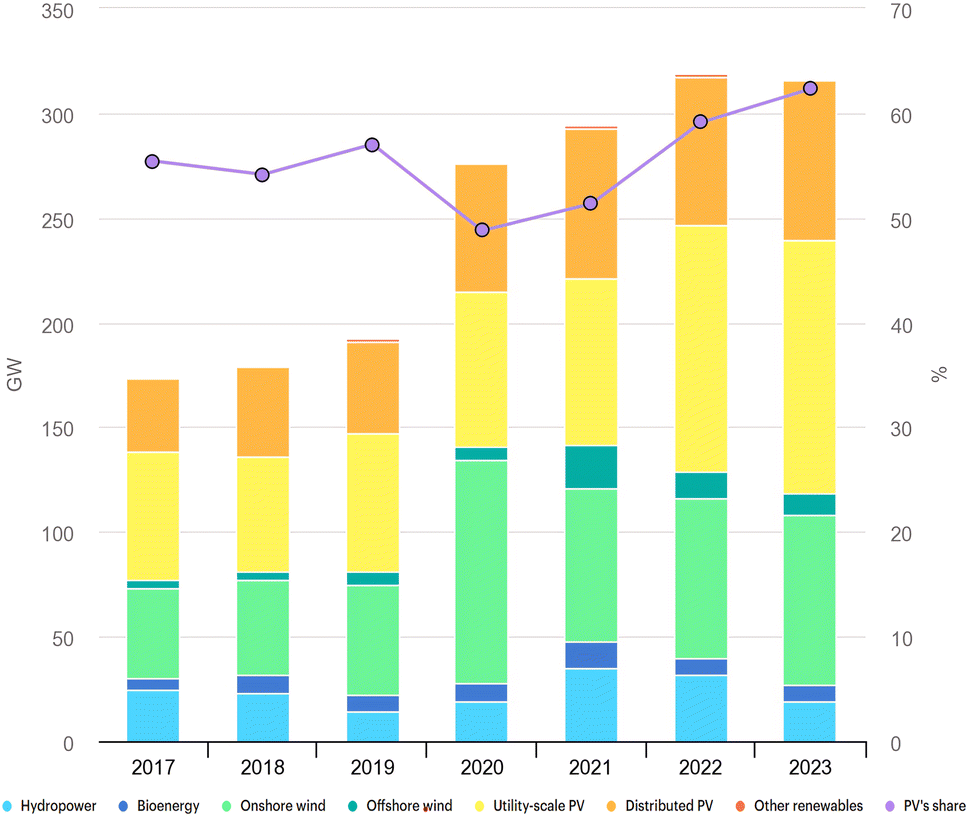

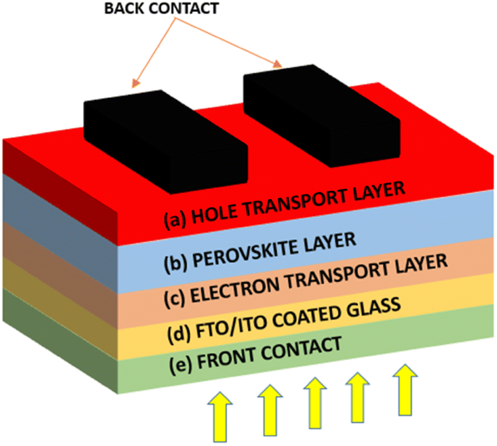
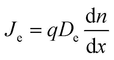
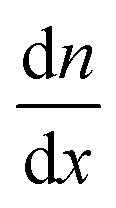 – density gradient in the direction of x.

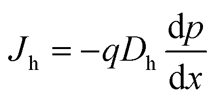
 – density gradient in the direction of x.