DOI:
10.1039/D3RA04759H
(Paper)
RSC Adv., 2023,
13, 28513-28526
Thermal stress-assisted formation of submicron pillars from a thin film of CoCrCuFeNi high entropy alloy: experiments and simulations
Received
15th July 2023
, Accepted 22nd September 2023
First published on 28th September 2023
Abstract
In this work, for the first time, the thermal stress-assisted formation of submicron pillars (SPs) from a high entropy alloy (HEA) thin film is made possible, and novel molecular dynamics (MD) simulations are proposed to assess the underlying mechanisms. In a series of experiments, the growth of quasi-equiatomic HEA SPs from CoCrCuFeNi HEA thin films was demonstrated under different heating and cooling conditions. Atomistic simulations are performed to probe possible formation mechanisms in two ways. One is to first obtain surface elastic constants and then conduct surface stability analysis with the consideration of size-dependent surface stress. The other is to effectively apply large compressive stress while simplifying the molecular dynamics (MD) model by using the Stoney equation to perform long-term MD simulations. From the former, it is suggested that surface diffusion is likely not the dominant cause for the observed pillar formation. From the latter, it is revealed that the level of compressive stress plays a much greater role than the crystalline structure of the film sample. Light has been shed on the stress-assisted formation of submicron pillars from CoCrCuFeNi HEA films by both experimental and simulation approaches.
1. Introduction
High-Entropy Alloys (HEAs) are defined as new kinds of alloys having more than five elements without a base element. This cutting-edge alloy family possesses versatile properties arising from the structural non-uniformity of multiple elements at the atom level.1–3 Those versatile properties include but are not limited to exceptional ductility at low temperatures, oxidation resistance, high strength/hardness, and radiation tolerance.2,4,5 Apart from serving as structural materials, HEAs are also candidates for superconductivity under certain conditions.6,7 Broadly speaking, those enhancements can be attributed to their intriguing properties such as high entropy, sluggish diffusion, lattice distortion, and cocktail effects.2 Although the CoCrCuFeNi HEA is in a simple face-centered-cubic (FCC) unit cell structure, its microstructure exhibits the presence of a Cu-rich phase due to the positive mixing enthalpies differently from the other elements.2 The atomic state of the CoCrCuFeNi system can depend significantly on the heating temperature and cooling speed because the synthesis of CoCrCuFeNi HEA itself can be achieved by the so-called rapid quenching effect.3
Compared with bulk counterparts, nanostructured HEA materials could be even more fascinating in terms of further enhanced mechanical performance,8,9 enhanced damage tolerance10,11 and other superior properties that bulk counterparts do not possess. To our knowledge, at least three types of nanostructures, namely, HEA nanopillars, nanoporous HEA and HEA nanoparticles have been successfully fabricated.12–15 NbMoTaW HEA nanopillars were successfully fabricated by using focused ion beams (FIB) to mill small-scale pillars (SPs).12 Due to the well-known size effect in nanomaterials, as predicted, such HEA pillar showed much higher yield strength than that of its bulk form. A method for making HEA nanoparticles with up to eight different elements has been developed,13 which relied on shocking metal salt-covered carbon nanofibers and followed by rapid quenching. By alloying–dealloying method, Jin et al.14 successfully fabricated nanoporous HEA with an ultrafine nano-ligament size of ≈2 nm, and the formation of quinary np-HEAs greatly enhances the electrochemical cycling stability due to the possible high-entropy effect and sluggish diffusion effect to achieve a record-high water splitting activity. A synthesis technique called the nebulized spray pyrolysis (NSP) method was introduced to produce the highly crystalline oxidized HEA powder, and it was found that the stabilization effect of entropy brought significant benefits for the storage capacity retention of HEAs and greatly improved the cycling stability.15 For aforementioned approaches to fabricating HEA nanomaterials, the utterly high cost such as in the case of FIB can be viewed as a drawback. In contrast, the stress-induced atom migration to fabricate nanopillar growth is a demonstrated low-cost approach for conventional metal nanowires.16 When a thin film experiences high-temperature heating, the difference in thermal expansion coefficients between the various components gives rise to a significant thermal stress difference, which leads to wire-shaped hillock formation at multiple length scales.17,18 The hillock volume in a unit area could be changed by the dependency of critical heating temperature and other influential factors. Intuitively, since such a stress-induced approach only applies mechanical stress to transport material, the mixture state of elements can be well-preserved. It could therefore be a promising low-cost approach to fabricating HEA SPs.
As noted in the review article written by the co-founder of HEAs,2 computational works are significantly lacking in the design and development of HEAs. According to the review paper, more than 30 metal elements had been successfully mixed to produce over 300 HEA combinations alone. Since each combination allows different composing concentrations, the acute possible HEAs are uncountable. This is totally different from nanowire growth in conventional metal films, in which experimental characterization would be enough since there is no concern about the universality. Facing such a challenge, we have limited our scope to mainly adopt a simulation and modeling approach to explain our experimental observations. The aim of this study is therefore to perform a series of experiments and atomistic simulations to demonstrate thermal stress-assisted CoCrCuFeNi HEA SPs and probe the underlying mechanisms. Observation of the micro-nano structure was conducted by scanning electron microscopy (SEM) and energy-dispersive X-ray spectroscopy (EDS). Since it is extremely difficult to measure the real-time surface growth and assess the instability of the surface due to surface diffusion experimentally, a novel modeling and simulation approach is hence employed to investigate pertinent mechanisms. Combining both experiments and simulations, new insights are offered to deepen our understanding of stress-induced atom migration in the case of CoCrCuFeNi HEA.
2. Experimental procedures
The CoCrCuFeNi HEA thin films with a thickness of ∼1 μm were synthesized on (1 0 0)-Si substrates by magnetron sputtering in an argon atmosphere of room temperature. The linear thermal expansion coefficient of the substrates is 2.63 10−6 K−1 at room temperature (≈300 K).19,20 The equiatomic Co20Cr20Cu20Fe20Ni20 HEA target (high purity: ≥99.99%) was used to deposit thin films. Before sputtering, the chamber was vacuumed below 5 × 10⁻⁴ Pa. The power of 100 W with a working pressure of 2.0 Pa was determined to generalize the composition and film thickness of ∼1 μm. Fig. 1(a and b) shows the cross-section view of SEM of Co20Cr18Cu23Fe19Ni20 HEA thin film as sputtered and an ideal structure of five elements. From the equiatomic Co20Cr20Cu20Fe20Ni20 HEA target, five elements were quasi-equivalently deposited as plotted in Fig. 1(c). After the sputtering of the thin films, heating, and cooling treatment were applied to induce thermal stress on the deposited films. The conditions are listed in Table 1.
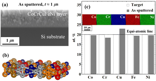 |
| | Fig. 1 Schematics of sputtered Co20Cr18Cu23Fe19Ni20 HEA thin film, (a) cross-section view of the film as sputtered, (b) ideal mixing of five atoms, and (c) elemental distribution of before and after sputtering from the equiatomic target. | |
Table 1 Heating temperature 800 °C and different cooling conditions
| Samples |
Heating |
Cooling method (cooling speed) |
| Temp. (°C) |
Time, h (increase/keep) |
Furnace atmosphere |
| Cooling in a glass tube with argon gas flow (300 SCCM) to room temperature. Cooling in a furnace with argon gas flow (300 SCCM) to room temperature. |
| A |
— |
— |
— |
— |
| B |
800 |
2/0.5 |
Argon gas |
Air in argon gasa (slow) |
| C |
800 |
2/4 |
Argon gas |
Furnace in argon gasb (intermediate) |
Sample A is as sputtered. To distinguish heating conditions, sample B was annealed to 800 °C for 2 h and kept for 30 min in a furnace. Sample C was treated for a relatively long holding time (4 h). The field emission SEM (JSM-7200F, JEOL, Japan) equipped with an EDS detector was used to characterize the microstructure and elemental state of films and SPs.
3. Experimental results and discussion
3.1 Thermal stress-assisted growth of CoCrCuFeNi HEA SPs
Regarding stress-assisted nanowire growth, thermal stress can be evaluated in three different ways. The first is the well-known X-ray diffraction (XRD) approach,21,22 which measures the crystal lattice spacing to evaluate the strain and then uses elastic constants to calculate stress. However, this approach can be problematic in our case due to the high entropy effect. The crystal lattice spacing before and after the heating can be significantly affected by the severe lattice distortion as a result of the high entropy state.23,24 The second way to measure thermal stress is to find the curvature of the film before and after the heating.25 However, considering the small size of the concerned film sample as well as the possible volume change due to oxidation, this approach is not feasible either in our case. The third way to measure the thermal stress is to apply the Stoney equation to the film-substrate structure or to implement the finite element calculation.26–28 In this study, the Stoney equation has been employed to evaluate the thermal stress due to the overwhelming difficulties in the aforementioned first two approaches. Nonetheless, in the future, we plan to adopt a combined approach of XRD and numerical modeling to exclude the effect of severe lattice distortion. SEM images of sample B in different scales were shown in Fig. 2 (a–d). Microstructure displays various hillock SPs, approximately at a length of ∼600 nm and a diameter of ∼300 nm. This was achieved under the heating and cooling condition of sample B (increased to 800 °C for 2 h and kept 0.5 h in argon gas and cooled in a glass tube with argon gas flow (300 SCCM) to room temperature. The corresponding top view is shown in Fig. 2(c and d). Surface morphologies show the convex protrusion with the width in an interval of ∼5 μm and roughness of ∼1.5 μm, in which the CoCrCuFeNi HEA SPs were revealed. The roughness measurement by atomic force microscopy (AFM) in Fig. 2(g) depicts the deepness between convex and concave. Fig. 2(e and f) show the elemental state of Cu and Fe. The convex and concave zones in Fig. 2(c and d) can be thought of as splits between the Cu-rich/Fe-lean zone and Cu-lean/Fe-rich zone by thermal stress-induced elemental rearrangement. It means that the CoCrCuFeNi HEA SPs tend to grow in Cu-rich/Fe-lean zones. In Fig. 2(h), different elemental distribution was plotted. The proportion of Co, Cr, and Ni was almost equivalent in at%, whereas that of Cu and Fe was significantly different as shown in Fig. 2(e and f).
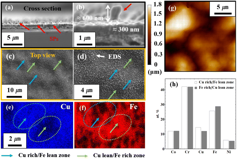 |
| | Fig. 2 Microstructure and elemental analysis of sample B, (a and b) SEM images CoCrCuFeNi HEA SPs in different scales of the cross-section view, (c and d) morphologies in different scales of the top view, (e and f) corresponding elemental analysis for Cu and Fe, (g) AFM image for the surface roughness, and (h) elemental distribution of Cu rich/Fe lean zone and Cu lean/Fe rich zone (at%). | |
3.2 Experimental identification of the growth mechanism
There are two growth mechanisms for nanowire growth as summarized in Chen et al.16 The grow-from-top pattern was observed in the case of metal oxide nanowires such as CuO nanowires. Although the driving force was the compressive stress generated from either the thermal expansion mismatch between the film and the substrate or the volume change due to oxidation, surface diffusion was considered the primary mechanism for transporting atoms. The grass-like tip is the direct evidence that surface diffusion has occurred there, and hence nanowire tips and sidewalls kept advancing in the concerned experiment. By comparison, HEA nanopillars observed here are not in a grass-like shape, and furthermore, their density is much lower than that of CuO nanowires.16 On the other hand, the grow-from-base pattern was observed in the case of metallic nanowires such as Al nanowires. Its driving force was the compressive stress between the film and substrate,29,30 which resulted in a direct extrusion of newly added length at the base from the so-called “weak spots” on the outer oxidation layer. The preservation of the tip and sidewall shape during the nanowire growth was strong evidence that surface diffusion was not much involved. In our case, the pillar morphology in Fig. 2(b) resembles that of the grow-from-base pattern closer than that of the grow-from-tip pattern. However, we were unable to observe a long enough nanopillar to confirm whether the tip shape was preserved. Also, observed HEA SPs in Fig. 2(b) appear considerably denser than those from the grow-from-base pattern, and yet significantly sparser than those from the grow-from-tip pattern. Based on all the experimental evidence gathered, the growth of HEA SPs appears more similar to the grow-from-base pattern than the grow-from-tip pattern. Nevertheless, we still cannot determine whether surface diffusion is likely the primary cause from an experimental perspective. Both the higher cost and the higher randomness involved in HEA materials than in conventional materials are obstacles for us to probe the growth mechanism experimentally in the current study. Both the HR-TEM and EBSD can help to further understand the growth mechanism. However, both the observation at the same site before and after nanopillar growth should be made. It would be meaningless if one only examines the grain boundary structure and defects by TEM and EBSD after the nanopillar growth because the formed grain boundary structure and defects are overwhelmingly likely a result of the nanopillar growth instead of the cause of the growth. Unfortunately, such TEM and EBSD observation would also be impossible to perform at the exact sites of nanopillar growth since these sites cannot be known before heating. Alternatively, we seek novel modeling and simulation approaches to resolve this difficulty. In the simulation and modeling, every condition is controllable such that the real-time “observation” of pillar growth at the same site can be carried out.
3.3 The role of heating and cooling conditions
The heating temperature is important in two ways. First, it determines the magnitude of the thermal stress. As the film was constrained by the substrate, a state of compressive stress was induced inside the film. On one hand, such compressive stress can drive atoms to exit from weak spots. On the other hand, existing weak spots on the outer oxide layer can be destroyed by too-large compressive stress. Second, surface diffusion can be very sensitive to temperature and temperature change. With a rapid change in temperature during cooling, the surface of HEA can evolve totally differently.3 Cooling conditions of the heating treatment with different temperatures are listed in Tables 1 and 2. Samples B and C in Table 1 were observed with the HEA SP growth, whereas all samples in Table 2 were not. This implies that the heating temperature is a deterministic factor in the HEA SP growth. As aforementioned, too-large compressive stress would break weak spots and hence make the growth of SPs impossible. Of course, HEA SPs cannot be grown with too-small compressive stress such as none in sample A. As not shown for brevity, the submicron pillar cannot be grown at a lower temperature such as 700 °C due to too small thermal stress. Nevertheless, in the future, we plan to investigate the optimal temperature for other HEA with different composing elements. Fig. 3 shows the evolution of surface morphologies under the variation in the cooling speed. It is revealed that HEA SPs can only be grown during the heating stage but not during the cooling stage. No matter what cooling speed was applied, samples in Table 2 cannot result in HEA SP growth. By comparison, once the heating temperature was appropriately chosen such as in Table 1, HEA SPs can be grown and kept under different cooling speeds. Unlike sample E, sample D was cooled in a glass tube with argon gas flowing into the atmosphere. Although neither sample led to SP growth, significant microstructure change was observed, which indicates the involvement of surface diffusion during cooling. A further increase in cooling speed of sample F led to the observed dendrites in Fig. 3(c). This is consistent with the rapid quenching effect in bulk HEAs.3
Table 2 Heating temperature 900 °C and different cooling conditions
| Samples |
Heating |
Cooling method (cooling speed) |
| Temp. (°C) |
Time, h (increase/keep) |
| D |
900 |
2/0.5 |
Air in argon gas (slow) |
| E |
900 |
2/0.5 |
Air (fast) |
| F |
900 |
2/0.5 |
Water (ultrafast) |
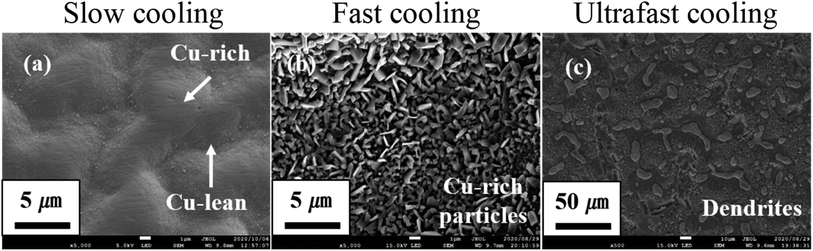 |
| | Fig. 3 SEM images of samples D, E, and F by different cooling speeds, (a) slow, (b) fast, and (c) ultrafast cooling. | |
4. Simulation methodology
As aforementioned, experimentally, it is extremely difficult to measure the real-time surface growth, assess the instability of the surface due to surface diffusion, or examine the mass flow with the given thermal stress. Local grain configuration in the experiment is neither possible to control. As an alternative, a novel modeling and simulation approach is hence employed to investigate pertinent mechanisms. In particular, MD simulation has been widely adopted in probing the pertinent deformation mechanism in HEA materials.31–37
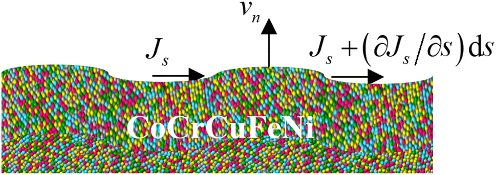
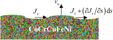
As aforementioned in the experimental part, two possible mechanisms among others to cause the formation of HEA SPs from the film should be examined. One is the surface diffusion due to the size-dependent surface stress (see Fig. 4),38,39 and the other is the stress-induced mass transport (see Fig. 5).
 |
| | Fig. 4 Surface instability due to surface diffusion with size-dependent size stress. | |
 |
| | Fig. 5 Long-term MD simulation of stress-induced mass transport. | |
4.1 Instability analysis of surface diffusion by quasi-static MD
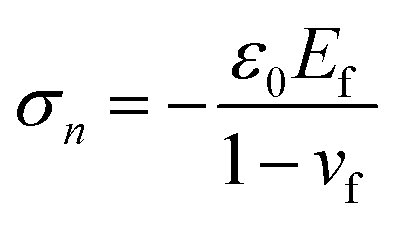
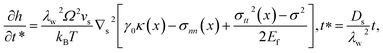
The instability analysis of surface diffusion by considering size-dependent surface stress is performed with the help of quasi-static MD in determining pertinent surface constants. The introduction of such surface stress in surface diffusion is deemed necessary in our case and has not been reported to our best knowledge. If unsuppressed, surface diffusion should be dominant since its diffusion coefficient is several-magnitude higher than that of bulk diffusion, namely, Ds = D in metallic materials. According to Srolovitz,38 the chemical potential μ of the diffusing species along an arbitrary interface in a stressed solid is given as| | |
μ = μ0 + Ωγ0κ − Ωσnn + ΩU.
| (1) |
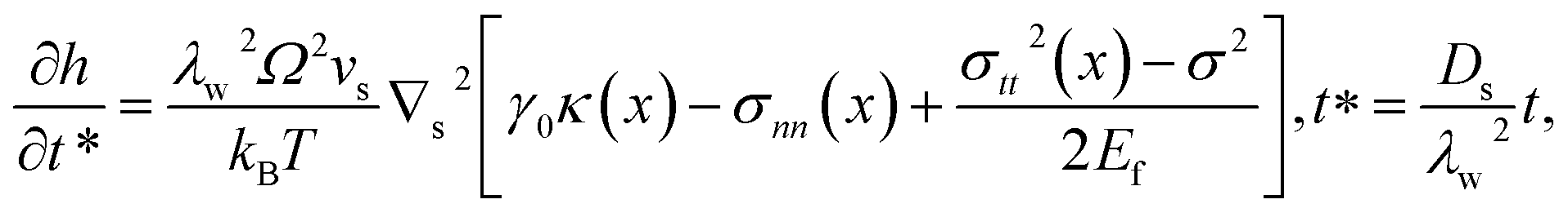
Here we denote the chemical potential of a flat CoCrCuFeNi HEA surface in equilibrium as μ0, the residual surface stress as γ0, the curvature as κ, the surface normal stress as σnn, the strain energy density as U and the atomic volume as Ω. The normal stress is retained here for the free surface due to the size effect.39,40 The resulting atomic flux from eqn (1) will lead to the change of surface profile h, which can be formulated as:38| |
 | (2) |
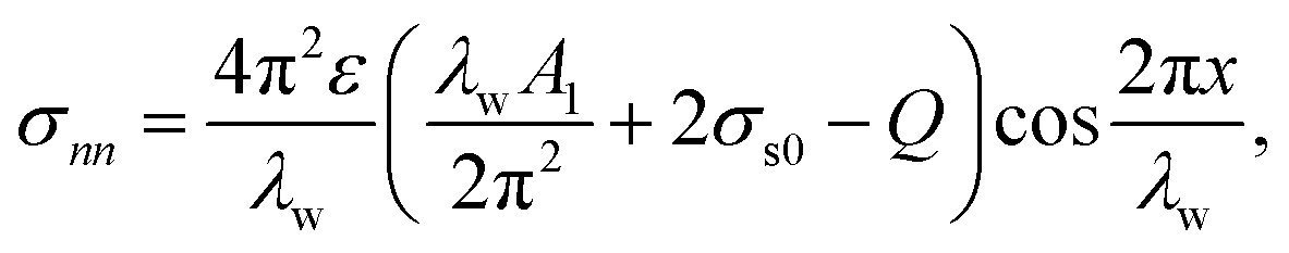
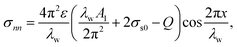
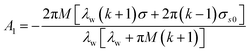
where Ds represents the surface diffusivity in CoCrCuFeNi, Ω is the atomic volume, νs = Ω−2/3 vis the surface atomic density, kB is the Boltzmann constant, T is the temperature and Ef is the Young's modulus of the film. Due to the uncertainty in the surface diffusivity of the diffusing species for CoCrCuFeNi, a characteristic time t* is introduced to avoid all the unknown constants in the case of CoCrCuFeNi.41 For the size-dependent surface stress on a small-amplitude, curved surface, namely, σnn and σnt, their analytical solutions are obtained by Grekov and Kostyrko42 via the perturbation method. Based on their solution, the stability of a cosine profile h(x) = −ελw![[thin space (1/6-em)]](https://www.rsc.org/images/entities/char_2009.gif) cos(2πx/λw) can be readily analyzed from the given normal stress and tangential stress.
cos(2πx/λw) can be readily analyzed from the given normal stress and tangential stress.| |
 | (3) |
| |
 | (4) |
Here λw is the wavelength of the surface asperity, ε is a small parameter and the rest dimensionless parameters are as follows| |
 | (5) |
| |
 | (6) |
| | |
σs0 = γ0 + M(1 + k)σ/4.
| (9) |
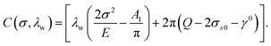
Following Srolovitz,38 a first-order approximation in eqn (2) can be taken as σtt2 − σ2 ≈ 2σ(σtt − σ). Meanwhile, the curvature of the surface can be approximated as κ(x) = −hxx/(1 + hx2)3/2 ≈ −hxx. To this end, the linear stability analysis, which is based on a small amplitude sinusoidal surface profile, can be performed. The partial differential equation (PDE) coefficient for the surface profile height, which depends on the applied stress σ and the wavelength λw of the surface, takes the form:
| |
 | (10) |
For the stable case C(σ,λw) < 0, the surface is to be flattened due to surface diffusion, whereas for the unstable case C(σ,λw) > 0, surface growth occurs.
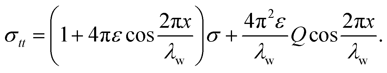
However, surface elastic constants for the above size-dependent surface stress still need to be determined by MD simulations, which is a common practice.43–45 So far, such simulations have not been reported for CoCrCuFeNi to our best knowledge. To start our simulations, two virtual samples with 10 × 40 × 40 and 20 × 40 × 40 crystal lattices are created. The thinner samples with three different crystal orientations are shown in Fig. 6. The surface energy Es can be extracted from the total energy by fitting the Etot data of different thicknesses h (with the same area A) into a linear function under the same applied strain.45
 |
| | Fig. 6 Stability of the CoCrCuFeNi surface under different wavelengths and applies stress. The dark green area indicates a stable state (surface asperity tends to shrink), while the yellow area indicates an unstable state (surface asperity tends to grow). Three crystalline orientations [1 0 0], [1 1 0] and [1 1 1] have been considered in (a), (b) and (c), respectively. | |
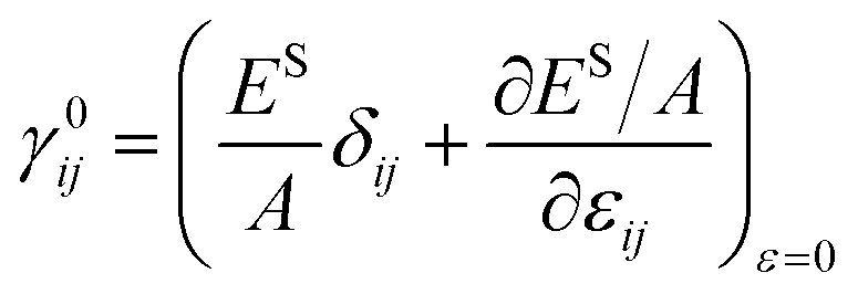
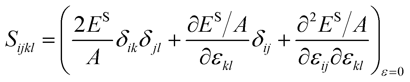
Simulations were run in a quasi-static fashion, which is performed with the software package LAMMPS46 adopting the EAM potential.47 Energy minimization is performed along with the relaxation of the simulation box. The relaxed configuration is then deformed to a strain of either −0.3%, 0% or 0.3% in the two periodic directions during 2000 steps with a time step of 1 fs. Afterward, the system is relaxed again by energy minimization. The finite difference method with second-order precision is then applied to derive the first-order derivatives and the second-order derivatives of the surface energy to obtain the residual surface stress γ0ij and the surface elastic tensor Sijkl.45
| |
 | (12) |
| |
 | (13) |
4.2 Stress-induced mass transport by long-term MD
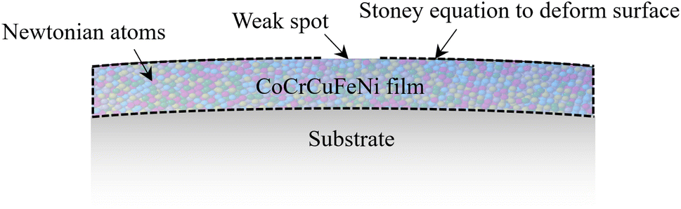
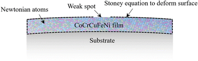
In this subsection, surface diffusion is ignored. It is known that surface diffusion can, for instance, be suppressed by the formation of surface oxides. In this scenario, the only mass transport comes from inside the film. It is commonly assumed this bulk flux exits at certain surface weak spots. For simplicity, we assume that the surface weak spots are pre-existing. To drastically save the computational cost, the deformation in the thin film due to its thermal expansion mismatch due to the substrate is given by the Stoney equations. Such a treatment eliminates the need to model the Si substrate, which is several orders of magnitude thicker than the film and would otherwise require a computational cost several orders of magnitude higher. According to the Stoney equation in the case of film-to-substrate thickness ratio hf/hs = 1, the induced compressive stress and the thermal strain mismatch are, respectively| |
 | (14) |
From eqn (14), displacement can be calculated and assigned as the prescribed displacement of surface atoms outside the weak spot in the MD simulation. To avoid unreal volume change in the film during simulation, it is preferable to apply Young's modulus, Poisson ratio, and thermal expansion rate of CoCrCuFeNi from corresponding MD simulations. From Table 3,37 the induced compressive stress is calculated to be 1.21 GPa. Under such compressive stress, barely any growth from the weak spot is observed since the time scale in the MD simulation is several magnitudes lower than the experimental time scale. To accelerate our MD simulation, artificial compressive stresses of 2.0 GPa, 4.0 GPa, 8 GPa or 16 GPa is applied to deform those surface atoms instead. It should be noted that the volume is preserved under the given compressive stress such that atoms are not simply squeezed out due to volume change.
Table 3 Parameters regarding Stoney equations
| |
Explanation |
Value |
| αf (K−1) |
The HEA film thermal expansion rate |
1.22 × 10⁻⁵ |
| αs (K−1) |
The substrate thermal expansion rate |
2.6 × 10⁻⁵ |
| ΔT (K) |
The temperature change |
780 |
| Ef (GPa) |
Young's modulus of the film |
95 |
| νf |
Poisson ratio of the film |
0.412 |
Table 4 Details of all CoCrCuFeNi virtual samples
| Sample |
Number of grains (under periodicity) |
Size (nm) |
Weak spot location |
| #1 |
2 |
7.88 × 15.3 × 14.0 |
Bi-crystal junction |
| #2 |
3 |
7.84 × 15.4 × 14.0 |
Triple junction |
| #3 |
6 |
8.85 × 17.7 × 17.7 |
Triple junction |
| #4 |
6 |
8.85 × 17.7 × 17.7 |
Quadruple junction |
| #5 |
6 |
8.85 × 17.7 × 17.7 |
Septuple junction |
| #6 |
6 |
8.85 × 17.7 × 17.7 |
Near a small grain |
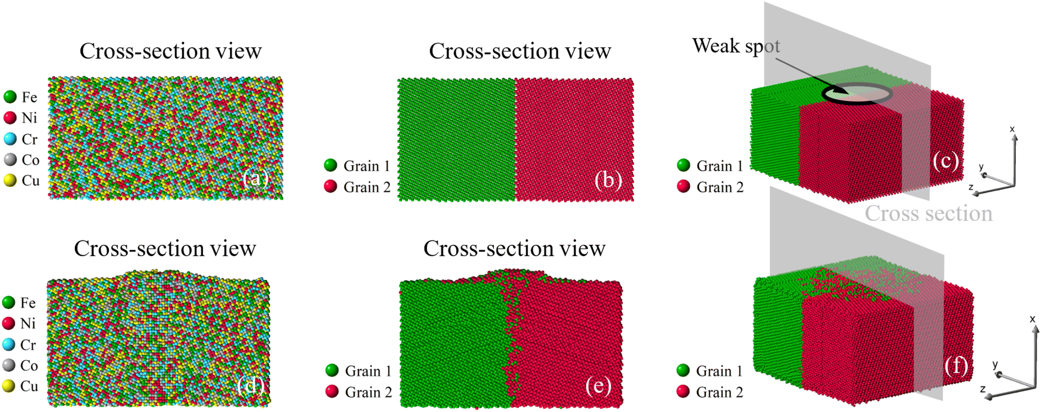
The CoCrCuFeNi samples are created by using the method stated in Cui et al.31 Once the CoCrCuFeNi geometry is generated, energy minimization is performed while allowing the simulation box to contract or expand. The sample then undergoes an equilibration run at the temperature of 1073 K for 4 × 10⁵ fsec under the NVT ensemble. At the same temperature, the move command of LAMMPS is used to slowly deform all surface atoms outside the circular weak spot over a period of 2 × 10⁸ fsec, until the level of the applied compressive stress has been reached. The details of all CoCrCuFeNi samples are described in Table 2. For the bi-crystal case, the crystal orientations for the two grains are x[0 2 1] y[0 −1 2] z[1 0 0] and x[0 2 −1] y[0 1 2] z[1 0 0], respectively. For the tri-crystal case, the crystal orientations for the three grains are x[0 2 1] y[0 −1 2] z[1 0 0], x[0 2 −1] y[0 1 2] z[1 0 0] and x[0 0 1] y[0 −1 0] z[1 0 0], respectively. The crystal orientations in all other cases are randomly assigned.
5. Simulation results and discussions
5.1 Instability analysis of surface diffusion by quasi-static MD
The obtained surface elastic parameters for the CoCrCuFeNi samples as shown in Fig. 6 are listed in Table 5 and they can be converted by considering relations λs = S1122 − γ011 and μs = (S1111 − S1122 + 2γ011)/2 to be used for surface stability analysis hence after. For the 2D surface stability analysis, S1122 is ignored.
Table 5 Surface elastic parameters of CoCrCuFeNi with different surface orientations
| c |
[1 0 0] |
[1 1 0] |
[1 1 0] |
| γ0 (eV Å−2) |
0.095 |
0.112 |
0.077 |
| S1111(eV Å−2) |
−0.604 |
−0.748 |
−0.106 |
The contour of whether C(σ,λw < 0) or C(σ,λw > 0) is plotted in Fig. 6. The dark green area indicates a stable PDE (no heterogeneous surface growth), while the yellow area indicates an unstable PDE (heterogeneous surface growth). Fig. 6 suggests that a CoCrCuFeNi pillar cannot be initiated from any submicron surface roughness under compressive stress smaller than about 750 MPa. As estimated in the preceding section, the concerned compressive stress is about 1.21 GPa. For such compressive stress, from Fig. 6(a)–(c), the threshold wavelengths, above which the surface instability occurs, are 650 nm, 850 nm, and 500 nm, respective for the three common crystal orientations [1 0 0], [1 1 0] and [1 1 1]. In other words, from the viewpoint of surface stability, only the formation of pillars with a diameter >500 nm should be due to surface diffusion. As observed in the experiment section, the typical diameter of the pillar is about 300 nm. Given the uncertainty in the measurement and in the estimation of stress, surface diffusion is likely not the dominant cause for the observed pillar formation.
5.2 Stress-induced mass transport
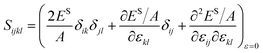
In Fig. 7, the growth of nano-asperity from the initial flat surface, which is measured by the atom with the highest vertical coordinate, is seen for all samples under the same compressive stress of 4 GPa. No strong correlation between growth and crystalline structure has been revealed. The largest final growth is observed for sample Case 4 consisting of six grains with a weak spot opened near a small grain. By comparison, sample Case 2 consists of six grains with a weak spot opened at the quadruple junction resulting in the smallest final growth. On one hand, the change in the grain number barely affects the growth of nano-asperity. On the other hand, Case 4 suggests that a small grain boundary near the weak spot may play some role.
 |
| | Fig. 7 Growth of nano-asperity versus time step for different virtual samples as listed in Table 4. The compressive stress is set as 4 GPa. | |
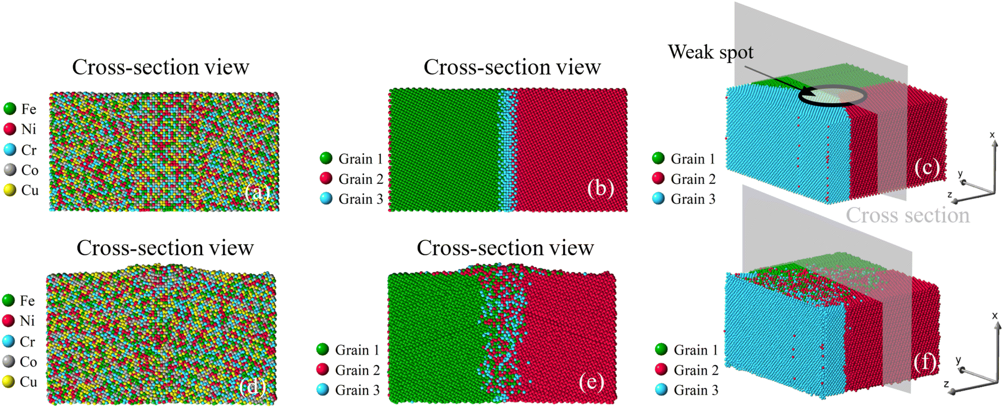
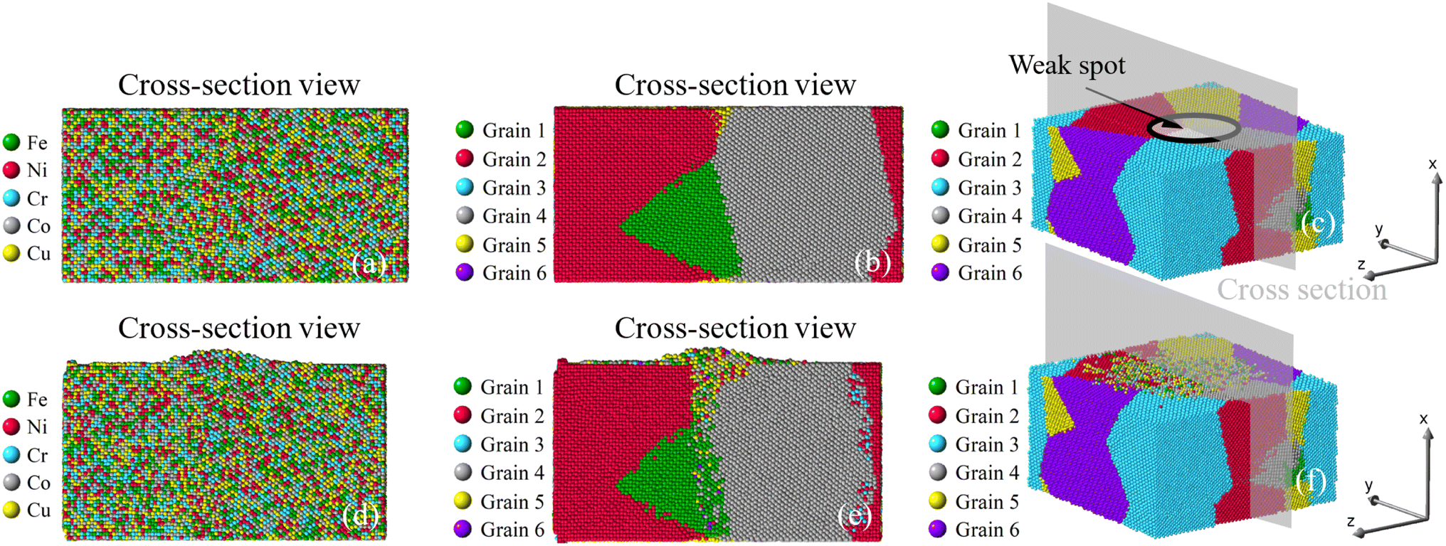
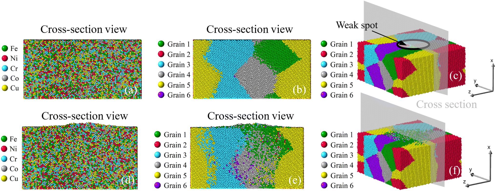
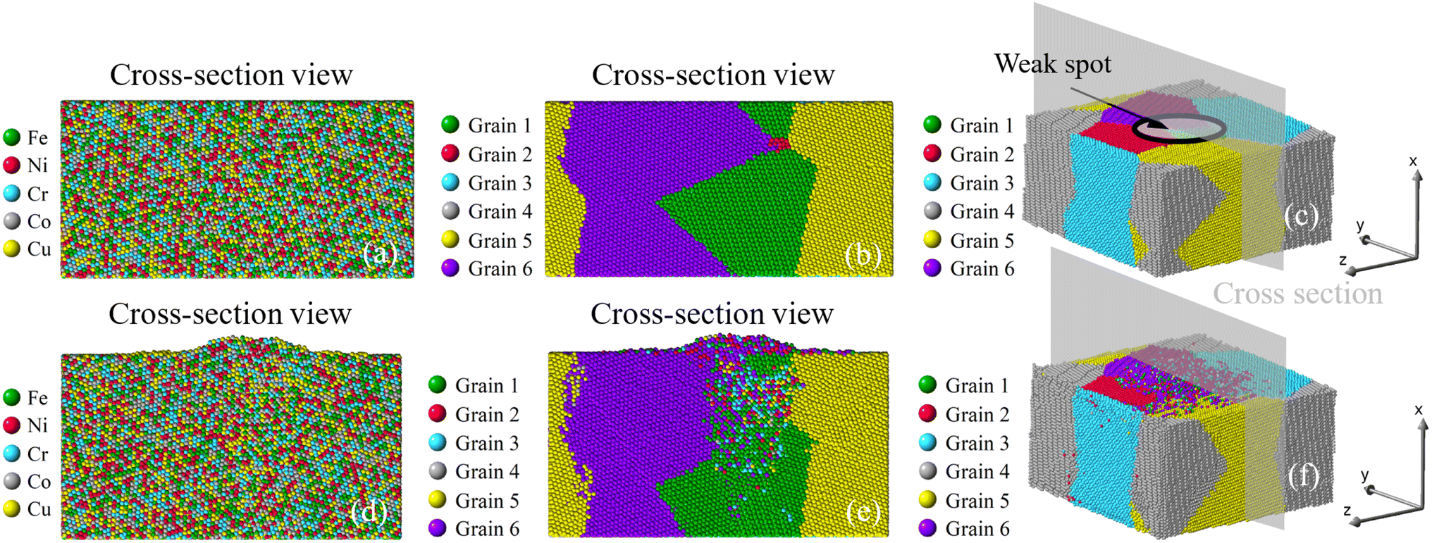
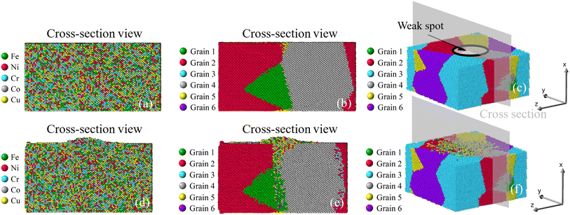
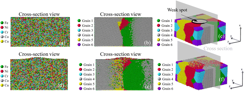
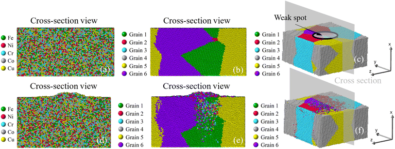
Corresponding to Fig. 7, the growth of nano-asperity from each sample is shown individually in Fig. 8–13, in which cross-section views are identified by either different elements or different grains. Overall, atoms are seen discharged through the weak spots to form nano-asperities. Notably, the film volume during simulation is preserved under the given compressive stress, so atoms are not simply squeezed out due to volume change. For all samples, no distinguishable pattern can be found in Fig. 8–13(a) when viewed by elements, and the atoms discharged from the film are in a well-mixed state. This can rather be favorable in that the formed nano-asperities can still be deemed as HEAs. Overall, our results reveal that the effect of grain and grain boundary configuration is insignificant compared with the level of applied compressive stress. For experiment, the difficulty in identifying the role grain boundary has played in pillar growth is that the exact sites of pillar growth cannot known before heating. The problem with only post-heating characterization is that the atomic structure in the grain boundary is overwhelmingly likely a result of the pillar growth instead of the cause of the pillar growth. Alternatively, in this study, our scope has been confined to applying simulation and modeling to probe the effect of grains and grain boundaries. As mentioned in the preceding subsection, the surface diffusion subject of size effect is also found not as a primary cause of the pillar growth since the surface is generally stable for our concerned conditions.
 |
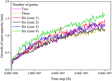
| | Fig. 8 Growth of nano-asperity from the bi-crystal sample. The cross-section views of the initial atomic configuration are identified by either different elements or different grains in (a and b), and (c) is the 3D view. Corresponding final configurations are shown in (d), (e) and (f), respectively. The compressive stress is set as 4 GPa. | |
 |
| | Fig. 9 Growth of nano-asperity from the tri-crystal sample. The cross-section views of the initial atomic configuration are identified by either different elements or different grains in (a and b), and (c) is the 3D view. Corresponding final configurations are shown in (d), (e) and (f), respectively. The compressive stress is set as 4 GPa. | |
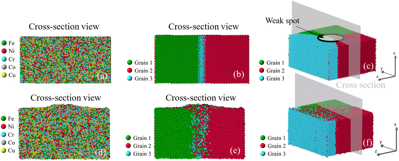
Once viewed by grains, two different patterns of mass transport can be observed from all six samples. The first pattern is recognized in the bi-crystal, tri-crystal, Case 2, and Case 3 of the six-grain samples, whose atom migration along and across grain boundaries occurs to all grains. The second pattern of mass transport, as recognized in Case 1 and Case 4 of the six-grain samples, takes place primarily at the grain boundaries beneath the weak spot by comparing Fig. 10(b) with Fig. 10(e) and Fig. 13(b) with Fig. 13(e), respectively. Except for the almost vertical one, the other two grain boundaries of the green grain in Fig. 10(e) exhibit very little intergranular atom migration. In Fig. 13(e), the atomic configuration surrounding and underneath the small green grain has varied significantly. In all 3D views in Fig. 8–13(c and f), atoms discharged from weak spots migrate along the top surface of film, which has caused nano-asperities to be flattened. Arguably, this should be different from surface diffusion since the time scale is insufficient.
 |
| | Fig. 10 Growth of nano-asperity from the sample consisting of six random grains (Case 1: weak spot at the triple junction). The cross-section views of the initial atomic configuration are identified by either different elements or different grains in (a and b), and (c) is the 3D view. Corresponding final configurations are shown in (d), (e) and (f), respectively. The compressive stress is set as 4 GPa. | |
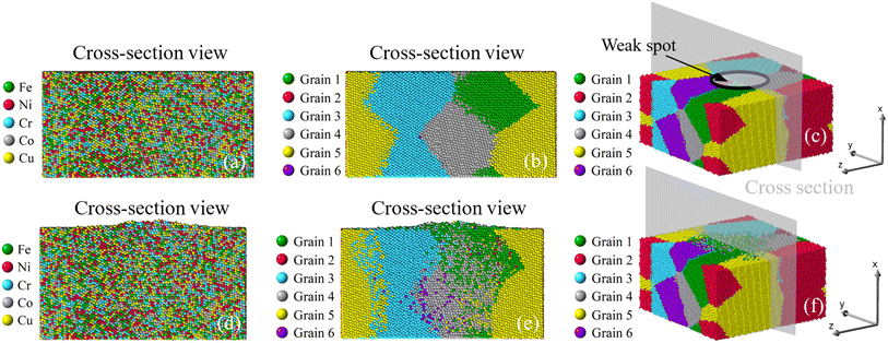 |
| | Fig. 11 Growth of nano-asperity from the sample consisting of six random grains (Case 2: weak spot at the quadruple junction). The cross-section views of the initial atomic configuration are identified by either different elements or different grains in (a and b), and (c) is the 3D view. Corresponding final configurations are shown in (d), (e) and (f), respectively. The compressive stress is set as 4 GPa. | |
 |
| | Fig. 12 Growth of nano-asperity from the sample consisting of six random grains (Case 3: weak spot at the septuple junction). The cross-section views of the initial atomic configuration are identified by either different elements or different grains in (a and b), and (c) is the 3D view. Corresponding final configurations are shown in (d), (e) and (f), respectively. The compressive stress is set as 4 GPa. | |
 |
| | Fig. 13 Growth of nano-asperity from the sample consisting of six random grains (Case 4: weak spot near a small grain). The cross-section views of the initial atomic configuration are identified by either different elements or different grains in (a and b), and (c) is the 3D view. Corresponding final configurations are shown in (d), (e) and (f), respectively. The compressive stress is set as 4 GPa. | |
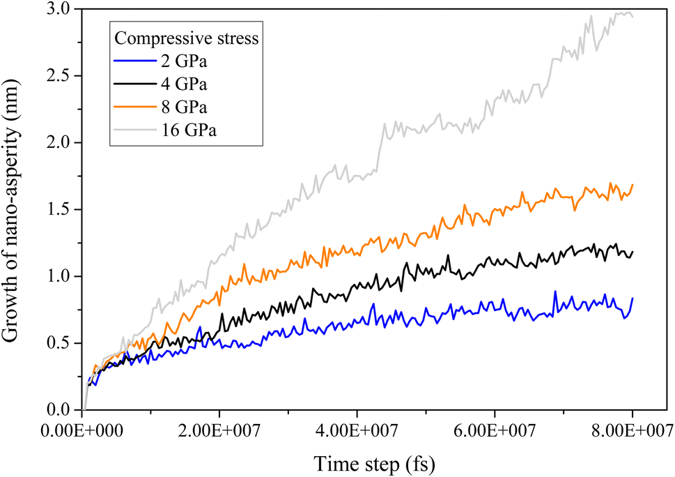
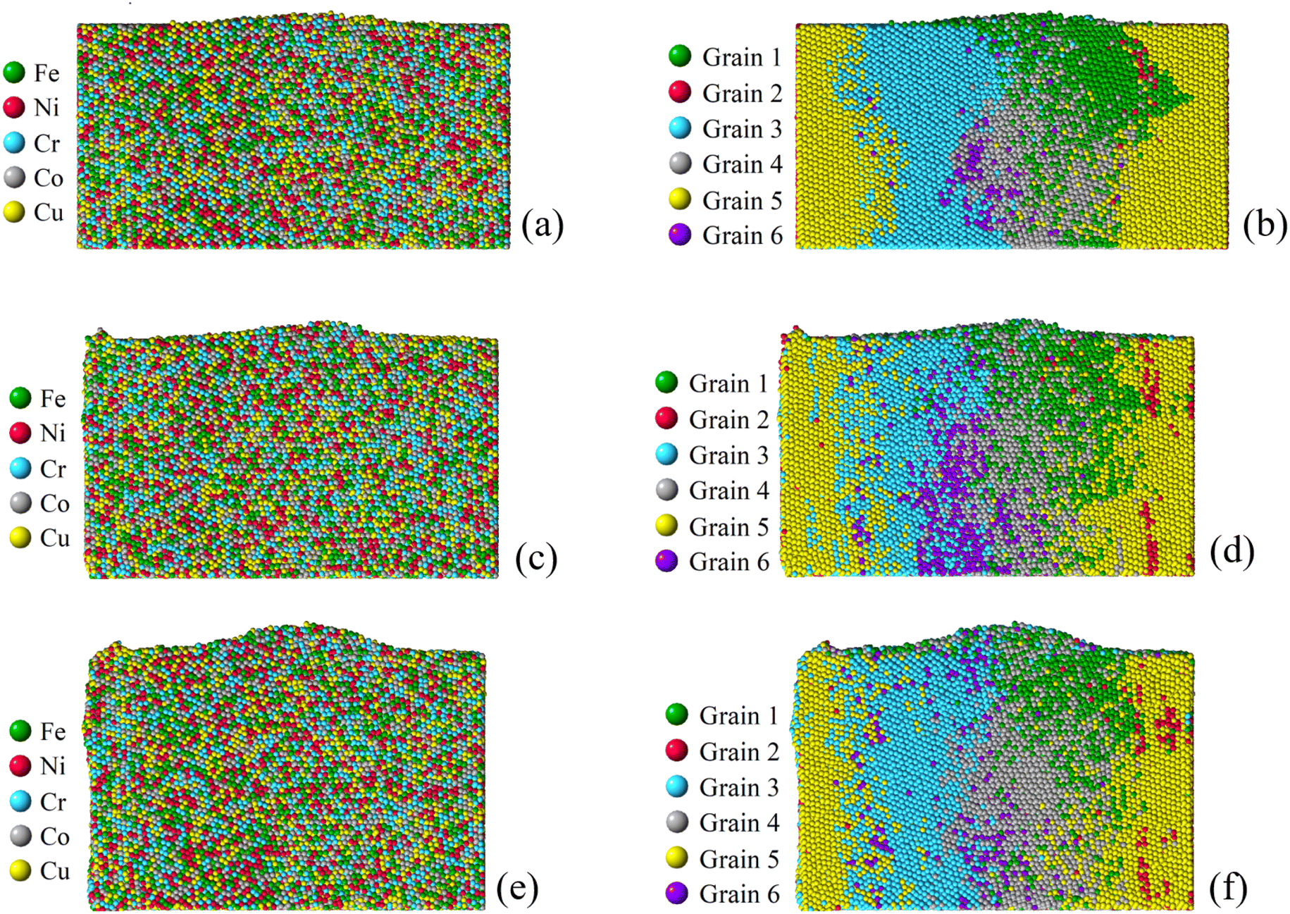
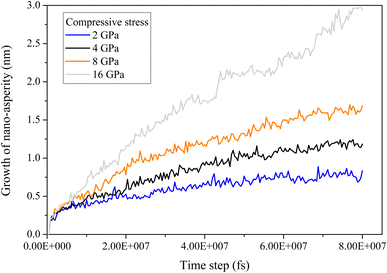
To investigate the role of compressive stress, three more simulations regarding Case 2 of the six-grain sample are conducted. Since its growth of nano-asperity is the smallest among all samples, if compressive stress can have a strong impact on it, the same strong impact (if not stronger) can be expected for all other samples. In Fig. 14, the impact of compressive stress is found to be indeed strong. The final growth of nano-asperity is roughly proportional to the applied compressive stress. The growth under 16 GPa is roughly twice that under 8 GPa. During simulation, the deformation from applying the compressive stress is gradually increased to the final value. In another sense, the rough proportionality indicates that our long-term simulation is not sensitive to the deformation rate, which is preferable. In Fig. 15, under the elevated compressive stress, no distinguishable pattern can be found when viewed by elements, and the atoms discharged from the film are also in a well-mixed state. Once viewed by grains, the same pattern of mass transport along and across grain boundaries of all grains can be observed. Due to the limitation in the simulation scale as a tradeoff to extend the time scale, the formation and evolution of large-scale structures of dislocation loops cannot be captured. Since it is well understood that prismatic dislocation loops can contribute to the hillock formation from films and dislocation loop-assisted mass transport48 has been observed on many other occasions, our future attention will be paid to such an investigation.
 |
| | Fig. 14 Growth of nano-asperity versus time step from the sample consisting of six random grains (Case 2: weak spot at the quadruple junction) under different compressive stress. | |
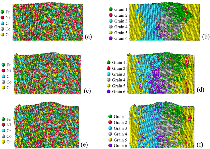 |
| | Fig. 15 Final growth of nano-asperity from the sample consisting of six random grains (Case 2: weak spot at the quadruple junction) under different compressive stress. Corresponding final configurations of differently identified atoms under a compressive stress of 2 GPa, 8 GPa and 16 GPa are shown in (a, b), (c, d) and (e, f). The simulation under a compressive stress of 4 GPa is shown previously. | |
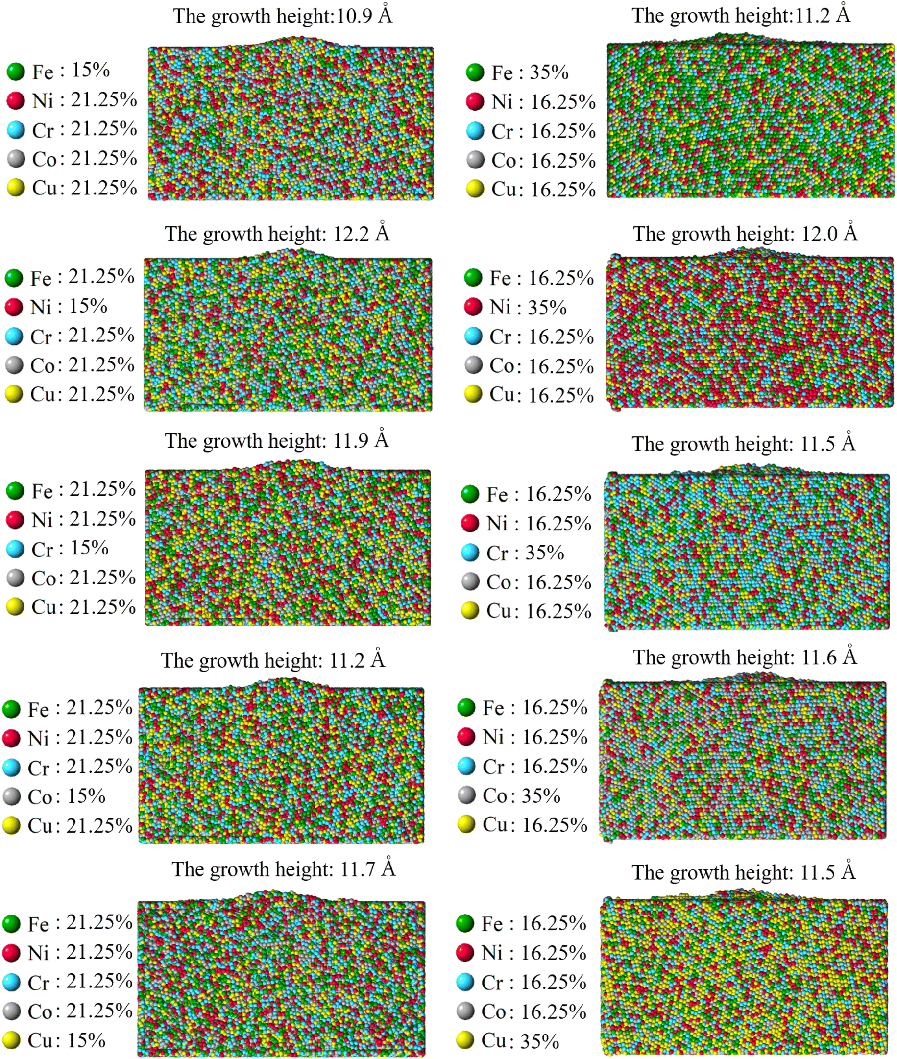
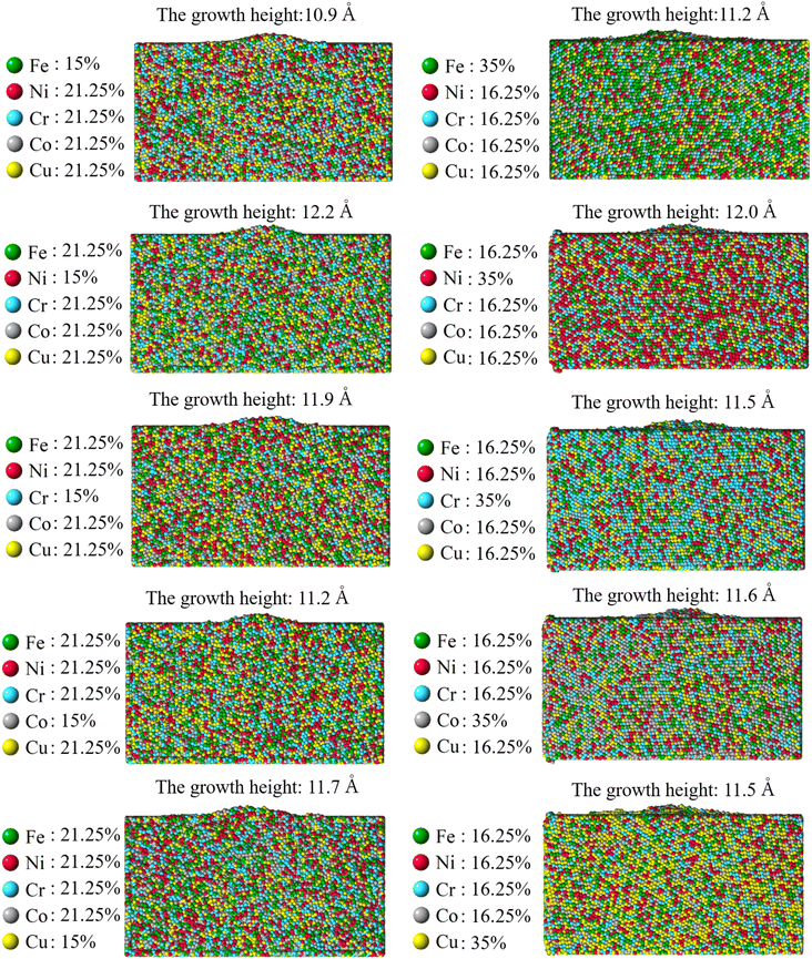
As for the influence of the element concentration, Fig. 16 reveal that the element concentration has a much weaker influence on the pillar growth than that of the applied compressive stress. Including the equiatomic CoCrCuFeNi, the concentration of each consisting element has been varied from 15% to 25% and to 35%. All other conditions like the grain configuration (Case 2: weak spot at the quadruple junction) and the magnitude of compressive stress has been made the same. Since the driving force is the compressive stress, the weak influence of the element concentration suggests that the stress-assisted approach is not selective to different types of atoms. This can be viewed as promising in that such method to grow submicron pillar can have universality to different composition of consisting element and potentially different HEA systems. Nonetheless, further experimental investigation should be conducted on other HEA systems in the future to help confirm the universality of the method.
 |
| | Fig. 16 Final growth of nano-asperity from the sample consisting of six random grains (Case 2: weak spot at the quadruple junction) with different element concentration. By definition, the concentration of each for HEA is between 5% and 35%. The CoCrCuFeNi HEA has been assumed equiatomic, i.e. the concentration of each element is 25% elsewhere in the paper. The compressive stress is set as 4 GPa. | |
6. Conclusions
In this work, we have investigated the fabrication of the thermal stress-assisted CoCrCuFeNi HEA SPs. Thermal stress and their relaxation with a possible surface diffusion process led to the hillock growth during which the mass transport by the compressive stress induced by different expansion coefficients between layers has played an important role. The applied heating temperature and cooling condition of sample B (annealed to 800 °C for 2 hours, kept for 30 min in a furnace) result in the successful fabrication of the CoCrCuFeNi HEA SPs (approximately a length of ∼600 nm and diameter of ∼300 nm). Atomistic simulations are conducted to determine possible formation mechanisms in two ways. One is to first obtain surface elastic constants and then carry out surface stability analysis with the consideration of size-dependent surface stress. The other is to effectively apply a large compressive stress while simplifying the molecular dynamics (MD) model by using the Stoney equation and then performing long-term MD simulations. From the former, it is revealed that surface diffusion is likely not the dominant cause for the observed submicron pillar formation. From the latter, it is suggested that the level of compressive stress has a greater impact than the crystalline structure of the film sample. For the first time, insights have been gained into the stress-assisted formation of submicron pillars from CoCrCuFeNi HEA films by combining both experiments and simulations.
Conflicts of interest
There are no conflicts to declare.
Acknowledgements
Funding from the Nitto Foundation is gratefully acknowledged. The experimental work was partly supported by a JSPS KAKENHI Grant-in-Aid for Challenging Research (Pioneering) No. 20K20531. It is also grateful to the JSPS KAKENHI Grant-in-Aid for Early-Career Scientists No. 23K13218.
References
- J.-W. Yeh, S.-K. Chen, S.-J. Lin, J.-Y. Gan, T.-S. Chin, T.-T. Shun, C.-H. Tsau and S.-Y. Chang, Adv. Eng. Mater., 2004, 6, 299–303 CrossRef CAS.
- M.-H. Tsai and J.-W. Yeh, Mater. Res. Lett., 2014, 2, 107–123 CrossRef.
- W. Li, P. Liu and P. K. Liaw, Mater. Res. Lett., 2018, 6, 199–229 CrossRef CAS.
- B. Gludovatz, A. Hohenwarter, D. Catoor, E. H. Chang, E. P. George and R. O. Ritchie, Science, 2014, 345, 1153–1158 CrossRef CAS.
- C. Lu, L. Niu, N. Chen, K. Jin, T. Yang, P. Xiu, Y. Zhang, F. Gao, H. Bei, S. Shi, M.-R. He, I. M. Robertson, W. J. Weber and L. Wang, Nat. Commun., 2016, 7, 13564 CrossRef CAS PubMed.
- P. Koželj, S. Vrtnik, A. Jelen, S. Jazbec, Z. Jagličić, S. Maiti, M. Feuerbacher, W. Steurer and J. Dolinšek, Phys. Rev. Lett., 2014, 113, 107001 CrossRef PubMed.
- J. Guo, H. Wang, F. Von Rohr, Z. Wang, S. Cai, Y. Zhou, K. Yang, A. Li, S. Jiang, Q. Wu, R. J. Cava and L. Sun, Proc. Natl. Acad. Sci. U.S.A., 2017, 114, 13144–13147 CrossRef CAS PubMed.
- W. Liao, S. Lan, L. Gao, H. Zhang, S. Xu, J. Song, X. Wang and Y. Lu, Thin Solid Films, 2017, 638, 383–388 CrossRef CAS.
- Z. F. Wu, X. D. Wang, Q. P. Cao, G. H. Zhao, J. X. Li, D. X. Zhang, J.-J. Zhu and J. Z. Jiang, J. Alloys Compd., 2014, 609, 137–142 CrossRef CAS.
- M. A. Tunes and V. M. Vishnyakov, Mater. Des., 2019, 170, 107692 CrossRef CAS.
- C. Dang, J. U. Surjadi, L. Gao and Y. Lu, Front. Mater., 2018, 5, 41 CrossRef.
- Y. Zou, H. Ma and R. Spolenak, Nat. Commun., 2015, 6, 7748 CrossRef PubMed.
- Y. Yao, Z. Huang, P. Xie, S. D. Lacey, R. J. Jacob, H. Xie, F. Chen, A. Nie, T. Pu, M. Rehwoldt, D. Yu, M. R. Zachariah, C. Wang, R. Shahbazian-Yassar, J. Li and L. Hu, Science, 2018, 359, 1489–1494 CrossRef CAS PubMed.
- Z. Jin, J. Lv, H. Jia, W. Liu, H. Li, Z. Chen, X. Lin, G. Xie, X. Liu, S. Sun and H. Qiu, Small, 2019, 15, 1904180 CrossRef CAS PubMed.
- A. Sarkar, L. Velasco, D. Wang, Q. Wang, G. Talasila, L. De Biasi, C. Kübel, T. Brezesinski, S. S. Bhattacharya, H. Hahn and B. Breitung, Nat. Commun., 2018, 9, 3400 CrossRef PubMed.
- M. Chen, Y. Yue and Y. Ju, J. Appl. Phys., 2012, 111, 104305 CrossRef.
- P. Chaudhari, J. Appl. Phys., 1974, 45, 4339–4346 CrossRef CAS.
- S. Hwang, W. Nix and Y. Joo, Acta Mater., 2007, 55, 5297–5301 CrossRef CAS.
- Y. Okada and Y. Tokumaru, J. Appl. Phys., 1984, 56, 314–320 CrossRef CAS.
- H. Watanabe, N. Yamada and M. Okaji, Int. J. Thermophys., 2004, 25, 221–236 CrossRef CAS.
- K. Kusaka, T. Hanabusa, M. Nishida and F. Inoko, Thin Solid Films, 1996, 290–291, 248–253 CrossRef CAS.
- M. Sobiech, U. Welzel, E. J. Mittemeijer, W. Hügel and A. Seekamp, Appl. Phys. Lett., 2008, 93, 011906 CrossRef.
- Y.-Y. Tan, T. Li, Y. Chen, Z.-J. Chen, M.-Y. Su, J. Zhang, Y. Gong, T. Wu, H.-Y. Wang and L.-H. Dai, Scr. Mater., 2023, 223, 115079 CrossRef CAS.
- J. Yi, M. Gharghouri, P. Bocher and M. Medraj, Mater. Chem. Phys., 2013, 142, 248–258 CrossRef CAS.
- D. S. Gardner and P. A. Flinn, J. Appl. Phys., 1990, 67, 1831–1844 CrossRef CAS.
- P. Sarobol, J. E. Blendell and C. A. Handwerker, Acta Mater., 2013, 61, 1991–2003 CrossRef CAS.
- E. Chason, N. Jadhav, F. Pei, E. Buchovecky and A. Bower, Prog. Surf. Sci., 2013, 88, 103–131 CrossRef CAS.
- P. Zhang, Y. Zhang and Z. Sun, J. Mater. Sci. Technol., 2015, 31, 675–698 CrossRef CAS.
- C. Chang and R. Vook, J. Mater. Res., 1989, 4, 1172–1181 CrossRef CAS.
- E. Iwamura, T. Ohnishi and K. Yoshikawa, Thin Solid Films, 1995, 270, 450–455 CrossRef CAS.
- Y. Cui, Y. Toku, Y. Kimura and Y. Ju, Scr. Mater., 2020, 185, 12–18 CrossRef CAS.
- Y. Cui, Z. Chen and Y. Ju, Materialia, 2020, 12, 100790 CrossRef CAS.
- Y. Cui, Y. Toku and Y. Ju, Nanotechnol, 2021, 32, 315716 CrossRef CAS PubMed.
- P. Wang, Y. Lin, Y. Cao, H. Zhao, Q. Li and H. Wang, Sci. China: Technol. Sci., 2023, 66, 998–1006 CrossRef CAS.
- T. Gao, H. Song, B. Wang, Y. Gao, Y. Liu, Q. Xie, Q. Chen, Q. Xiao and Y. Liang, Int. J. Mech. Sci., 2023, 237, 107800 CrossRef.
- C. J. Ruestes and D. Farkas, Comput. Mater. Sci., 2022, 205, 111218 CrossRef CAS.
- C. J. Ruestes and D. Farkas, J. Mater. Sci., 2021, 56, 16447–16462 CrossRef CAS.
- D. J. Srolovitz, Acta Metall., 1989, 37, 621–625 CrossRef.
- M. E. Gurtin and A. Ian Murdoch, Int. J. Solids Struct., 1978, 14, 431–440 CrossRef.
- M. E. Gurtin, J. Weissmüller and F. Larché, Philos. Mag. A, 1998, 78, 1093–1109 CAS.
- K. Forsberg and A. R. Massih, Modell. Simul. Mater. Sci. Eng., 2007, 15, 335–353 CrossRef CAS.
- M. A. Grekov and S. A. Kostyrko, Int. J. Solids Struct., 2016, 96, 153–161 CrossRef.
- R. E. Miller and V. B. Shenoy, Nanotechnol, 2000, 11, 139–147 CrossRef CAS.
- P. Sharma, S. Ganti and N. Bhate, Appl. Phys. Lett., 2003, 82, 535–537 CrossRef CAS.
- V. B. Shenoy, Phys. Rev. B: Condens. Matter Mater. Phys., 2005, 71, 094104 CrossRef.
- S. Plimpton, J. Comput. Phys., 1995, 117, 1–19 CrossRef CAS.
- D. Farkas and A. Caro, J. Mater. Res., 2018, 33, 3218–3225 CrossRef CAS.
- Y. Cui, Z. Chen and Y. Ju, Comput. Mater. Sci., 2018, 155, 400–409 CrossRef CAS.
|
| This journal is © The Royal Society of Chemistry 2023 |
Click here to see how this site uses Cookies. View our privacy policy here. 
 Open Access Article
 This Open Access Article is licensed under a Creative Commons Attribution-Non Commercial 3.0 Unported Licence
 a,
Yasuhiro Kimuraa,
Shaojie Gua,
Yuhki Tokua,
Yang Jua and
Yi Cui
a,
Yasuhiro Kimuraa,
Shaojie Gua,
Yuhki Tokua,
Yang Jua and
Yi Cui