
 Open Access Article
 This Open Access Article is licensed under a Creative Commons Attribution-Non Commercial 3.0 Unported Licence
Unravelling the surface structure of β-Ga2O3 (100)
Alex Sandre Kiliana,
Abner de Siervo b,
Richard Landersb,
Guilherme Jean P. Abreuc,
Mayron S. Castrob,
Tyson Backd and
Alexandre Pancotti*a
b,
Richard Landersb,
Guilherme Jean P. Abreuc,
Mayron S. Castrob,
Tyson Backd and
Alexandre Pancotti*a
aInstituto de Ciências Exatas e Tecnológicas/Grupo de Física de Materiais, Universidade Federal de Jataí, BR 364, km 195, No. 3800, 75801-615, Jataí, Goias, Brazil. E-mail: apancotti@ufj.edu.br
bInstituto de Física “Gleb Wataghin”, Universidade Estadual de Campinas, Campinas 13083-859, SP, Brazil
cDepartamento de Física, Universidade Federal do Paraná, Caixa Postal 19044, 81531-980, Curitiba-PR, Brazil
dAir Force Research Laboratory, 2179 12th Street, B652/R122, WPAFB, Ohio 45433-7718, USA
First published on 21st September 2023
Abstract
The present work is on a comprehensive surface atomic structure investigation of β-Ga2O3 (100). The β-Ga2O3 single crystal was studied by a structural model system in the simulations and in situ characterization via X-ray photoelectron spectroscopy (XPS), low-energy electron diffraction (LEED) and X-ray photoelectron diffraction (XPD) allowed for probing the outermost layers' properties. In situ XPD characterization allows for the collection of valuable element-specific short-range information from the β-Ga2O3 surface, and the results were compared to a systematic and precise multiple scattering simulation approach. The experiments, characterizations, and simulations indicated strong evidence of considerable structural variations in the interatomic layer's distances. Such atomic displacement could clarify the electronic phenomena observed in theoretical studies. The comparison between experimental and theoretical XPD results involving multiple scattering calculations indicated that the β-Ga2O3 surface has two possible terminations. The best fits to the photoelectron diffraction curves are used to calculate the interplanar relaxation in the first five atomic layers. The results show good agreement with previous density functional theory calculations, establishing XPD as a useful tool for probing the atomic structure of oxide surfaces.
Introduction
Ga2O3 is an ultrawide bandgap (UWBG) semiconductor oxide material, with an ultrawide-bandgap (UWBG) ranging from 4.5–5.3 eV. Compared to other semiconductor materials, for example SiC (3.3 eV) and GaN (3.4 eV), Ga2O3 has a larger band gap, and good chemical stability. Additionally, Ga2O3 has a theoretical breakdown electric field at 8 MV cm−1, being three times larger than that of either SiC or GaN, and a large Baliga's figure of merit (BFOM).1 This makes Ga2O3 particularly useful for power electronic applications, where extreme environments such as high temperature, high radiation, high voltage, and high current are a concern. For these reasons, Ga2O3 has been investigated for use in power transmission, rail traction, hybrid propulsion, rail guns, and Schottky barrier diodes.2–4Ga2O3 is a polymorph material that can have six crystalline phases, known as α, β, γ, δ, ε and κ. The β-Ga2O3 is the most stable thermodynamically, even at 2023 K. The formation energy of the polymorphs has the following order β < ε < α < δ < γ.3 β-Ga2O3 has the monoclinic structure with the space group C2/m or C2h3 space group (number 12).5 Fig. 1 shows the conventional unit cell of β-Ga2O3. The Ga atoms are at two crystallographic inequivalent positions, one in the tetrahedral geometry Ga(I), and the other in the octahedral geometry Ga(II). The oxygen ions are arranged in three crystallographic different positions O(I), O(II), and O(III), where O(I) and O(II) oxygen atoms are coordinated trigonally and O(III) is coordinated tetrahedrally, all of them situated at 4i(x,0,z) positions at the Cs group symmetry plane. The crystalline structure may be described as GaO6 octahedra centered at Ga(II) atoms, sharing and linked oxygen atoms with GaO4 tetrahedra centered at Ga(I) atoms.6–8 The melting point for the β-Ga2O3 is 2067 K, and considering this temperature of β-Ga2O3, the cost of production of substrates becomes cheaper than other semiconductors materials in bulk crystals, such as GaN and SiC.3
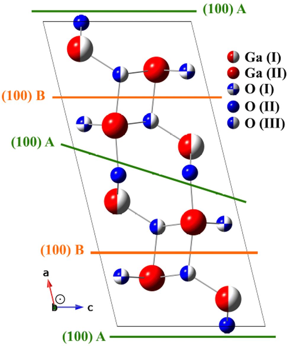 | ||
| Fig. 1 Conventional unit cell of monoclinic (C2/m) β-Ga2O3. The two different gallium (large red spheres) positions and the three inequivalent oxygen (little blue spheres) positions are illustrated. The possible stable surface termination (100) A and (100) B. | ||
Recent works show the possibility of β-Ga2O3(100) exfoliation. The [100] is the most studied and applied in this case and yielding very thin films and preserving the pristine bulk-like electronic properties, which makes it even more promising for applications in power devices.9,10 Kim et al.10 have obtained quasi-2D Ga2O3 flakes from bulk β-Ga2O3 through mechanical exfoliation, and until now, some phenomena's and properties have been studied on the β-Ga2O3 (100) considering the possibility of yield a 2D Ga2O3, majority of this studies in a theoretical view. Su et al.13 investigate the exfoliation process along some low index surfaces planes, and obtained exfoliation energies. It was observed the exfoliation energy for monolayer Ga2O3 (100) surface is lower than (010) and (001) surfaces planes, since the lattice parameters and Ga–O bonds lengths for [100] direction are larger than in the other directions, which results in the 2D monolayer being formed more readily in the (100) orientation compared to (010) and (001) orientations. Theoretical predictions about the so-called 2D Ga2O3,11,12 show a promising possibility of applications, since in these systems, it was observed physical properties that differ from bulk material, such as the electron mobility of bilayered β-Ga2O3, being several orders of magnitude higher than β-Ga2O3. This feature extends the applications of Ga2O3 in electronic and optoelectronic devices.13,14
Bermudez5 performed ab initio theory with Hartree-Fock calculations for the slab relaxations of low index surfaces planes, such as (100), (010), (001) and (10−1). The β-Ga2O3(100) was shown to have5 two possibilities of surface terminations (100) A and (100) B while the β-Ga2O3(010) only had one surface termination. For the (010) plane it was observed the distances between Ga(I) to O(I), O(II), and O(III) on the surface are shorter than the bulk value. Anam et al.38 used DFT calculations to show the 4.00 eV band gaps for Ga2O3 (100) with bilayer Ga2O3. These results demonstrate the importance the surface terminations have on electronic properties. Pancotti et al.20 performed XPD (X-ray photoelectron diffraction) experiments with (MSCD) multiple scattering calculation diffraction and DFT calculations. This study shows the significant displacements in the first topmost slab surface, moreover, this calculation shows an important rumpling between gallium and oxygen atoms in the topmost surface slabs, for β-Ga2O3(010).
Regarding 2D Ga2O3 and Bulk like β-Ga2O3 (100) there is some disagreement between theoretical and experimental observations,5,16–18 moreover the different preparation methods used for the production of the surface may promote other surfaces configurations, such as the enrichment of Ga and/or O vacancies, and consequently variations in interplanar distances at surfaces.5,15,19–22 For experimental studies, the ultra-high vacuum (UHV) methodologies with surface science are adequate to extract structural and electronic parameters of surface, but in the same time, it is a challenge to obtain this information straight forwardly via in situ experiments. Therefore, the goal of this work is to characterize the surface structure of β-Ga2O3 (100) in situ with surface science techniques.
To the best of our knowledge, there are no experimental studies with X-ray photoelectron diffraction (XPD) with the β-Ga2O3(100) surface structure. In this study, we have prepared a clean β-Ga2O3(100) surface which were characterized with X-ray photoelectron spectroscopy (XPS) and low-energy electron diffraction (LEED), and applied in situ XPD structural characterization. XPD has been strongly applied to clarify the surface structures of thin films, molecules on substrates, and two-dimensional materials systems. XPD provides information about atomic arrangements at the surface being element-sensitive and chemical state-specific. A complete understanding of the bond angles, the orientation of adsorbed molecules, and bond distances is obtained by comprehensive multiple scattering simulations.23–25
The results extracted from XPD experiments and simulations from the clean β-Ga2O3(100) surface indicated strong relaxations in the topmost layer of surfaces, promoting almost coplanarity of the first three outmost surface layers in the model B.
Experimental section
The experiments were performed at the surface science system, equipped with Omicron HA-125HR, a hemispherical high-resolution electron analyzer with a fixed geometry, LEED optics. The sample holder was able to heat the sample up to 1300 K and the manipulator there are five degrees of freedom, 3T (x, y, z) and 2R (θ, ϕ) allowed in. The coordinates (x, y, z) moves the sample in the 3D directions and the (θ, ϕ) are the polar and azimuthal angle rotations. The β-Ga2O3(100) substrate used in this study was grown by the Czochralski method and supplied by Sojitz Machinery Corporation,™ with a size of (10 × 10 × 0.5) mm3. The analysis of the as-received sample by XPS and LEED showed small carbon peak on the surface, observed by XPS, yielding a sharp LEED pattern from the β-Ga2O3(100), denoting the ordered surface. The substrate was cleaned by annealing at 800 K for 30 min in vacuum (UHV) to minimize the surface C contamination. The XPS was performed using the non-monochromatic Mg Kα X-ray source. The XPS spectra were fitted using Gaussian-type functions, where each peak is composed of 50% Gaussian and 50% Lorentzian line shape with Shirley background subtracted. After the surface characterization by LEED and XPS, the β-Ga2O3(100) surface was analyzed by XPD using photons from the Mg Kα X-ray source. XPD measurements were performed acquiring XPS spectra from O 1s, with kinetic energy (Ek) of 723 eV core-level for the β-Ga2O3(100) surface. During all XPD and XPS measurements, the base pressure was kept below 7 × 10⁻¹⁰ mbar. XPD experiments were performed in the angle scanned mode. For the O 1s measurements, it was varied the θ polar angle in steps of 3° from 18° to 54°, while the azimuthal angle (ϕ) was varied in 3° steps from 0° to 180°, and replicated in XPD pattern (only for visualization purpose) to complete the 360°.Theoretical XPD patterns were simulated taking into account multiple scattering in the fourth-order for the Rehr–Albers approximation26,27 and multiple scattering up to the sixth order. The simulations were performed once for photoemission peak of O 1s core-level. The multiple scattering simulations considered a cluster that consisted of approximately 380 atoms with a depth range to 30 Å and a top radius of 8 Å in a paraboloid shape. The muffin-tin potential for Ga, and O atoms in their respective β-Ga2O3(100) bulk phases were used to obtain the phase shifts and radial matrix for the scattered electrons.
The structural parameters are determined in a fit procedure that searches for the set of parameters that optimizes the agreement between the theoretical and experimental diffraction curves, through minimization of the reliability factor Ra, defined as the difference between the experimental and the simulated diffraction patterns:
The quantities χci and χei are the calculated and experimental photoelectron diffraction anisotropies, respectively. The smaller the Ra factor, the better the agreement with experiment, with 0Ra1. A perfect agreement correspond to Ra = 0, no agreement is expressed by Ra = 1. The sum in the Ra equation is over all angles in the data base.
In the search for the lowest Ra factor, the non-structural parameters Debye temperature (TD) and inner potential (V0), were allowed. The interlayer distances (relaxation) were optimized for O and Ga layers (d12 to d45), where dij is the interlayer distance between the topmost layer i and its subsequent layer j. According Fig. 1, the interlayer distances between the layers composed by Ga and O in the [100] described for a B model terminated as d12 distance between O(III) and O(I) layers, the d23 distance between O(I) and Ga(II), d34 distance between Ga(II) and Ga(I) and d45 distance between Ga(I) and O(II), for the optimized termination B, and for the termination A is described the d12 as distance between O(II) and Ga(I) layers, the d23 distance between Ga(I) and Ga(II), d34 distance between Ga(II) and O(I) and d45 distance between O(I) and O(III). The reliability factor Ra24 from the normalized XPD intensities was used to compare the experimental and simulated XPD patterns. The quantified agreement is the so-called Ra factor. The uncertainty – is about 0.05 Å considering the statistical analysis of the Ra factor.20,28
Results and discussion
Fig. 2(a) shows a sharp LEED pattern at 188 eV. The LEED image shows a characteristic rectangular surface lattice and confirms the high ordering for β-Ga2O3(100) surface.17 Fig. 2(b) shows XPS survey spectra of β-Ga2O3(100) of the clean sample surface. The spectra show β-Ga2O3(100) characteristics peaks and do not show significant surface contamination, such as carbon located at 284.6 eV in binding energy (Eb). The surface carbon atomic concentration was estimated at 4%. The intensities for this calculation consider the relative sensitivity factors of analyzed atoms and the analyzer transmission. Fig. 3(a and b) shows the XPS for Ga 2p3/2 and O 1s with binding energy of peak positions at 1118 eV and 531 eV, respectively. These values are consistent with positions previously reported for β-Ga2O3.29–31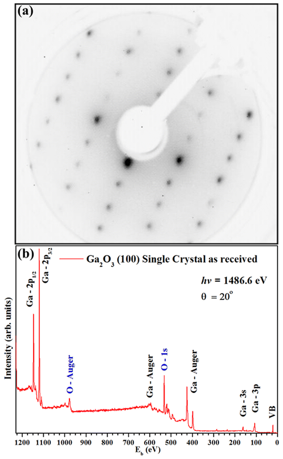 | ||
| Fig. 2 (a) LEED patterns (188 eV) and (b) XPS survey spectra for the clean β-Ga2O3 (100) sample surface. | ||
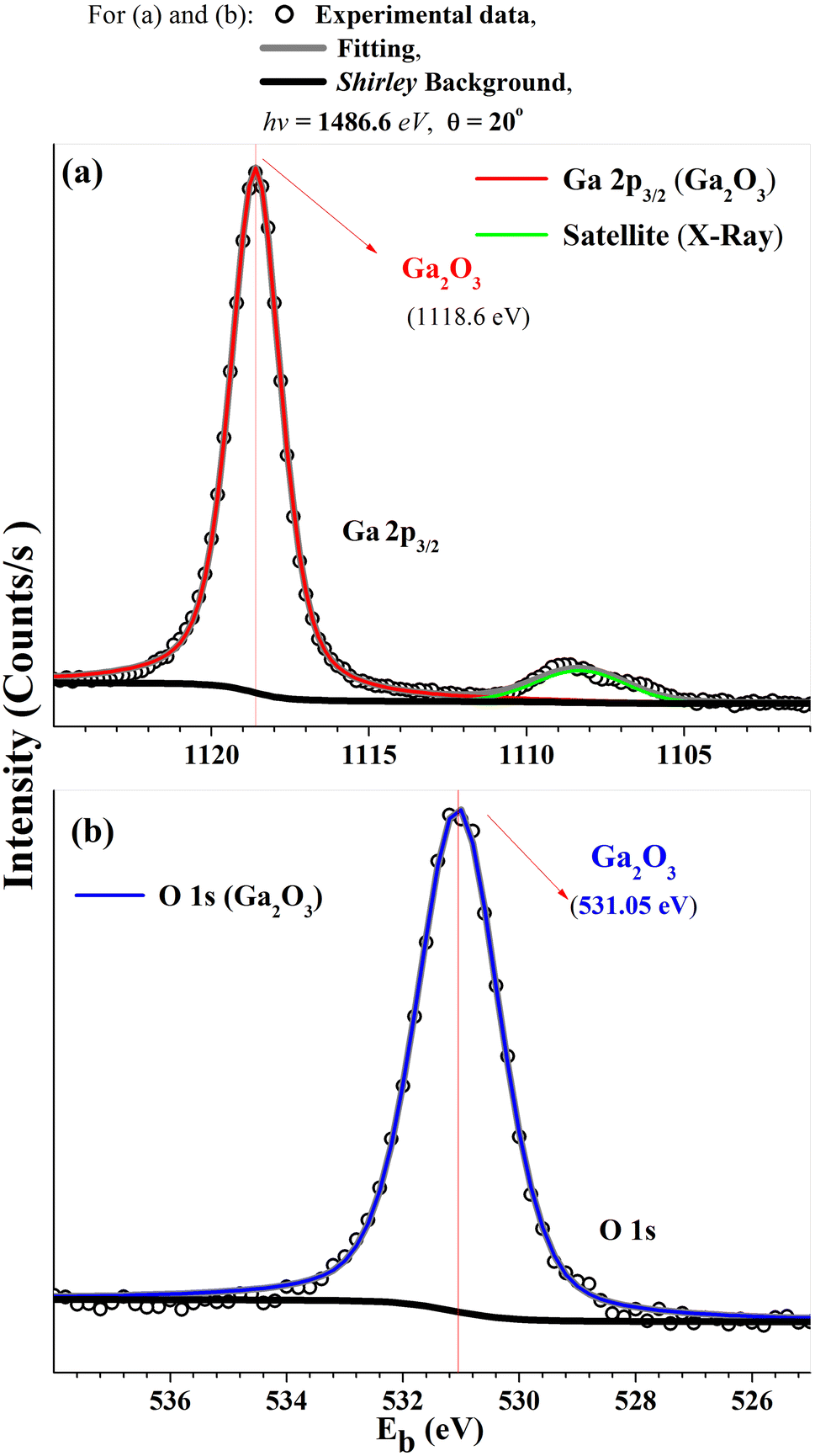 | ||
| Fig. 3 HRXPS for (a) Ga 2p3/2 and (b) O 1s XPS regions from β-Ga2O3(100) sample surface. | ||
After the characterizations of β-Ga2O3(100) surface by XPS and LEED, the experimental XPD patterns were collected using O 1s (Fig. 4(a)) as emitter. The theoretical XPD patterns were simulated considering the O 1s as emitter with a kinetic energy of 723 eV, where forward scattering regime dominates. For the O 1s XPD measurements, the forward scattering provides more sensitivity toward the position and directions of atoms on the surface structure. A higher intensity of collected photoelectrons from the surface is represented by the brighter spots in the XPD pattern. The two or four-fold symmetry is observed in all patterns, which is expected for this surface plane. These XPD patterns are in agreement with the LEED patterns shown in the Fig. 2(a).
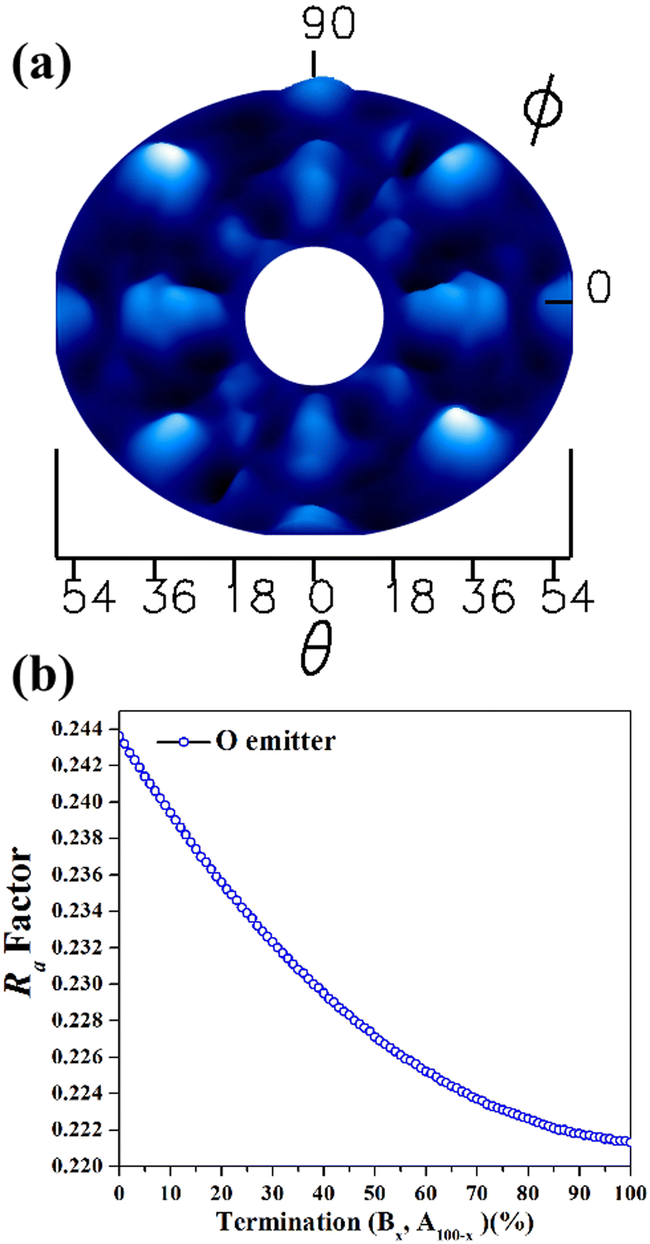 | ||
| Fig. 4 (a) Experimental XPD pattern obtained from the β-Ga2O3(100) sample surface for O 1s and (b) Ra factor values as a function of termination A and B in the β-Ga2O3 (100) surface, considering O as emitter atoms. | ||
As previously discussed there are two possibilities of termination for β-Ga2O3(100),5 one termination called A: terminated in rows of oxygen, lying along the [010] direction with each oxygen back-bonded to two with Gallium, and B termination: where terminated in nearest-neighbor rows of gallium and oxygen atoms, each singly-unsaturated. These two terminations were proposed for the following simulations, and in the first, it were proposed the bulk value for interlayer distances, considering the vectors of the unit cell with values a = 12.452 Å; b = 3.083 Å; c = 5.876 Å, β = 103.68°.32,33 The Ra factor obtained were Ra = 0.244 for termination called A and Ra = 0.220 for B termination.
Since Ra factors are close for both terminations, the following step was conducted to verify the predominance of the A and B termination on to β-Ga2O3(100). Two model structures were used for the linear combination: one consisting of an A termination of β-Ga2O3(100) and the other representing B termination, with bulk values for interlayer distances. The linear combination was carried out using MSCD, taking into account O 1s as emitters and considering all angles (18° to 54°). Fig. 4(b) shows the Ra factor versus linear combination for B and A termination. The smallest Ra factor in the Fig. 4(b) is referring to 100% predominance of B termination, however Ra factor difference between A an B terminations is too small to unambiguously determine the surface predominance. The experimental work published by Lovejoy17 and co-authors showed that areas of the B termination constitute most of the surface, while areas of the A termination are small and confined to near step edges.
Considering the small difference in the Ra factor in the two surface terminations and the Ra factor value denoting good agreement between theory and experiment, we carried out the surface relaxations for both, A and B surface terminations for β-Ga2O3(100).
As a first step, the non-structural parameters were relaxed, such as Inner potential (V0) and Debye temperature (TD). The values obtained were 750 K and 13 eV, for TD and V0 respectively. This is in good agreement with values previously reported in the literature.18,34
After this step, relaxations of d12, d23 d34 and d45 interlayer distances for the β-Ga2O3(100) A terminated were performed. These relaxations were performed in the same way as B termination for the search for a lower Ra factor. The intervals of interlayer distances applied during minimization process were as follows: d12 (0.77 Å to 1.63 Å) and d23 (0.04 Å to 1.07 Å), d34 (0.00 Å to 0.12 Å) and d45 (0.06 Å to 0.36 Å).
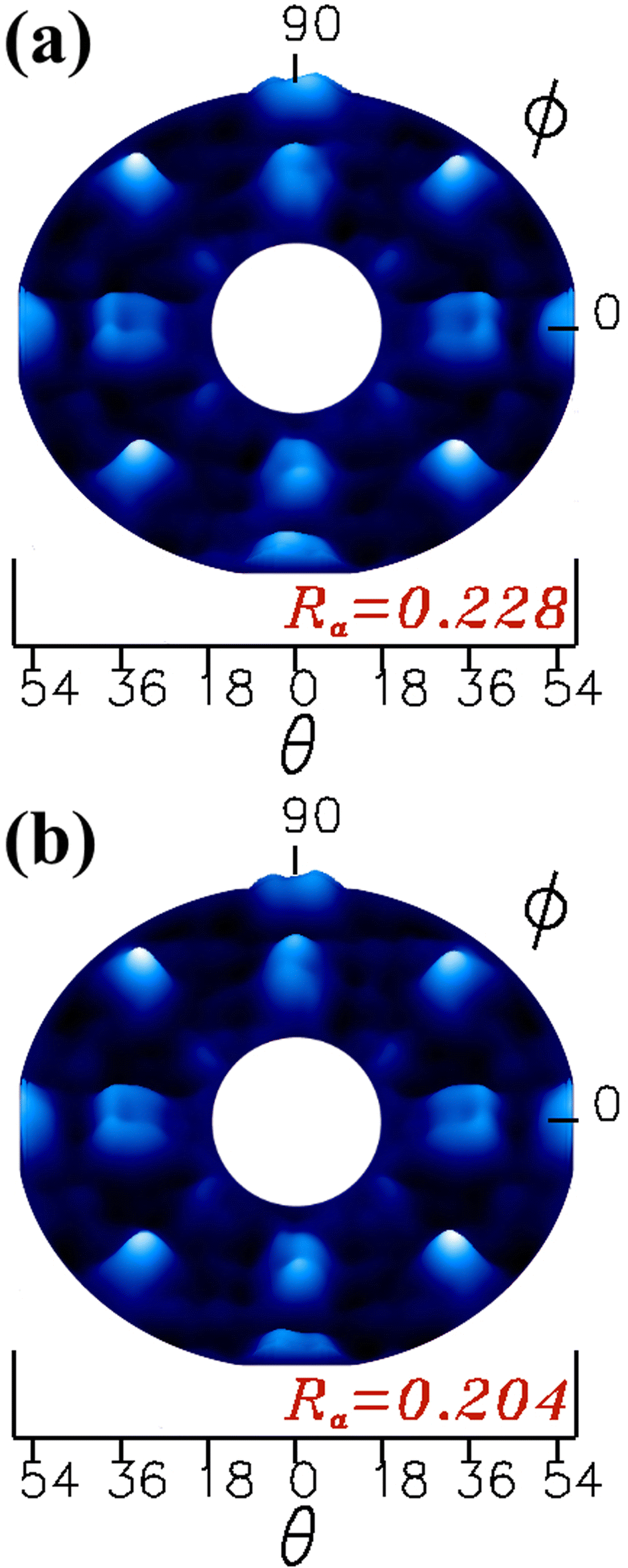
Fig. 5(a) shows the d12 and d23 interlayer distances in the search for the best Ra factor. The lowest Ra factor obtained was resulted in d12 = 1.47 Å (+42.6%), d23 = 0.56 Å (−32.3%). These two interlayer distances (d12 and d23) were fixed during the d34 and d45 optimizations. The Fig. 5(b) shows the d34 and d45 interlayer distances in the search for the best Ra factor. The lowest Ra factor refer to interlayer distances d34 = 0.064 Å (+5.1%) and d45 = 0.20 Å (+71.6%). The bonding distance obtained with these structural relaxations were O(II)–Ga(I) 2.13 Å, Ga(I)–O(III) 1.745 Å, Ga(I)–O(I) 1.806 Å, Ga(II)–O(III) 1.967 Å, Ga(II)–O(III) 1.967 Å, Ga(II)–O(I) 2.118 Å. The Ra factor achieved for these relaxed interlayer distances was Ra = 0.228.
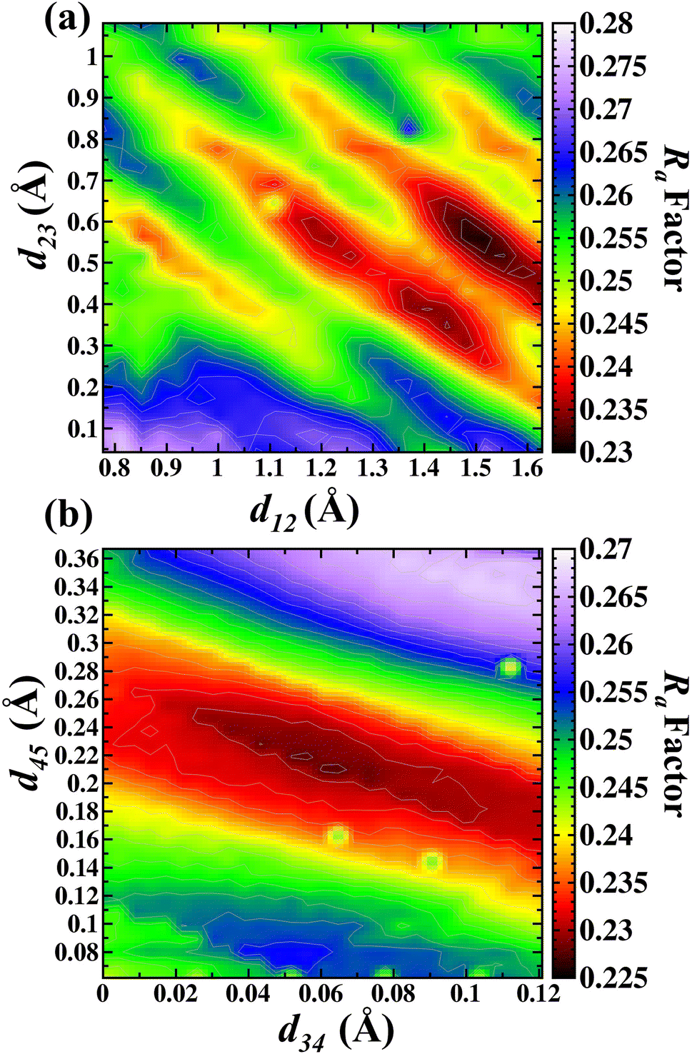 | ||
| Fig. 5 Contour map in the search of lowest Ra factor for (a) d12 versus d23 and (b) d34 versus d45 for the A termination. | ||
In our study the d12 expansion was observed, which is in contrast with previous work which showed the contraction of the outmost oxygen O(II) toward the Ga(I).5 It was previously shown that the d23 is the distance between the Ga(I) and O(I), having a contraction of 0.07 Å for this interlayer distance, toward these layers in direction to the surface.5 In our study the distance between Ga(I) and O(I) contract from the 0.89 Å to 0.62 Å (−29%). The distance O(I) and Ga(II) achieved in our study was from a bulk value of 0.062 Å to 0.065 Å, with an expansion of +5%. Simulations performed with the DFT calculations5 showed an expansion between the third and fourth atomic layer (d34), represented by O(I) and Ga(II). Finally, the d45 or Ga(II) and O(III) layer is achieved with an expansion of 0.01 Å.5 In this work the distance was from 0.18 to 0.20 Å, and the observed expansion is in agreement with Bermudez.5
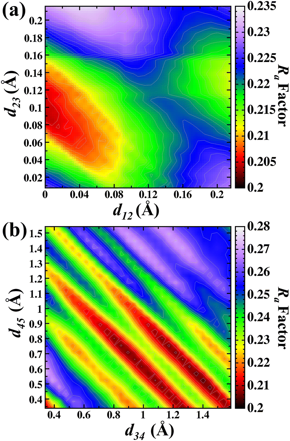
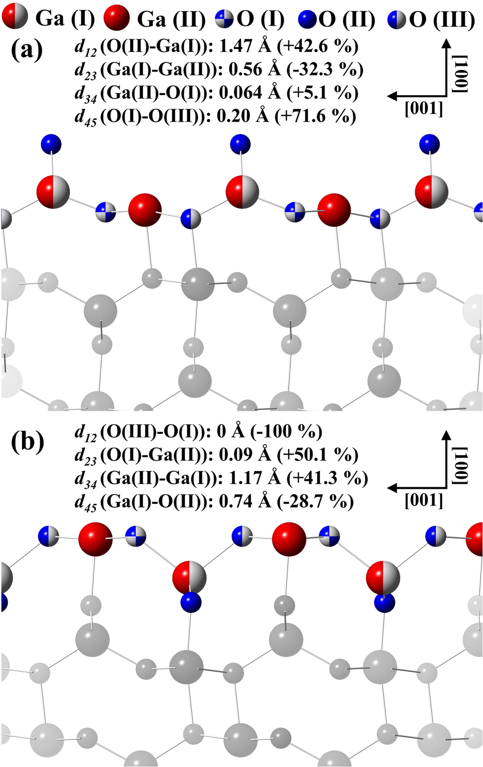
In the next step, relaxations of d12, d23 d34 and d45 interlayer distances for the β-Ga2O3(100) surface structure, termination B model were realized. These relaxations were performed in the same way as A termination for the search of lower Ra factor. These relaxations were varied and performed at the same time in the search for the lower Ra factor, using O atoms as emitters. The relaxation optimizations were done with 0.01 Å steps for the search for d12 and d23, and 0.05 Å steps for d34 and d45. The limits of interlayer distances applied to the search were as follows: d12 and d23 (0.00 Å to 0.21 Å), d34 and d45 (0.15 Å to 1.54 Å).
Fig. 6(a) shows the d12 and d23 interlayer distances in the search for the best Ra factor. The lowest Ra factor obtained was for d12 = 0 Å (−100%), d23 = 0.09 Å (−50.1%). In the next step, the values obtained for d12 and d23 were then kept fixed and the optimization of the d34 and d45 interlayer distances was carried out. The Fig. 6(b) shows the d34 and d45 interlayer distances in the search for the best Ra factor. The lowest Ra factor yielded interlayer distances of d34 = 1.17 Å (+41.3%) and d45 = 0.74 Å (−28.7%). The bonding distance obtained with these structural relaxations were Ga(II)–O(III) 1.968 Å, Ga(II)–O(I) 2.102 Å, Ga(I)–O(I) 2.04 Å, Ga(I)–O(II) 1.711 Å and Ga(I)–O(III) 2.06 Å. The Ra factor achieved for these relaxed interlayer distances was Ra factor: 0.204.
 | ||
| Fig. 6 Contour map in the search of lowest Ra factor for (a) d12 versus d23 and (b) d34 versus d45 for the B termination. | ||
The surface plane (100) with B termination, for β-Ga2O3 is the most stable surface termination compared with the other terminations for the low index planes, such as (100) A, (010) and (001). Other experimental18,35 and theoretical13,21 works find this same behavior. Our results agree with these studies since the lowest Ra factor (Ra = 0.220) for bulk interlayer distances shows that the most likely termination describing the surface is β-Ga2O3(100) B.
The interlayer differences in this study differ from those found previously.5 Considering the behavior of displacements for O(I), O(III) and Ga(II) for the study of Bermudez, our results show similar coplanarity in the topmost surface. Bermudez has shown an expansion for the d34, and a little contraction between the distances formed by Ga(II) and Ga(I), represented by d34.
The bonding distances obtained in our study show slightly larger values compared with previous work.5,35 Additionally, similar expansions in the bonding distance was observed by Barman et al.,9 who used ab initio calculations to study β-Ga2O3(100).9
Changes in the atomic interlayer distances of the Ga2O3 for the first five atomic layers as determined by the O 1s XPD simulations are shown in the Table 1. Negative values indicate a contraction in the interlayer distance, whereas positive values indicate an expansion into the relative bulk value. All displacements are in Å.
| Interlayer distance | A – terminated | B – terminated |
|---|---|---|
| Ra = 0.228 | Ra = 0.204 | |
| d12 | 1.47(+42.6) | 0(−100) |
| d23 | 0.56(−32.3) | 0.09(−50.1) |
| d34 | 0.064(+5.1) | 1.17(+41.3) |
| d45 | 0.20(+71.6) | 0.74(−28.7) |
Fig. 7 compares simulated and experimental azimuthal scans, from 246° to 66°, at selected polar angles, for both A and B model terminations. It demonstrates excellent agreement for the curves measured at polar angles between 24° and 51°. Model B shows lower Ra factors for all range of angles (bulk and surface sensitive).
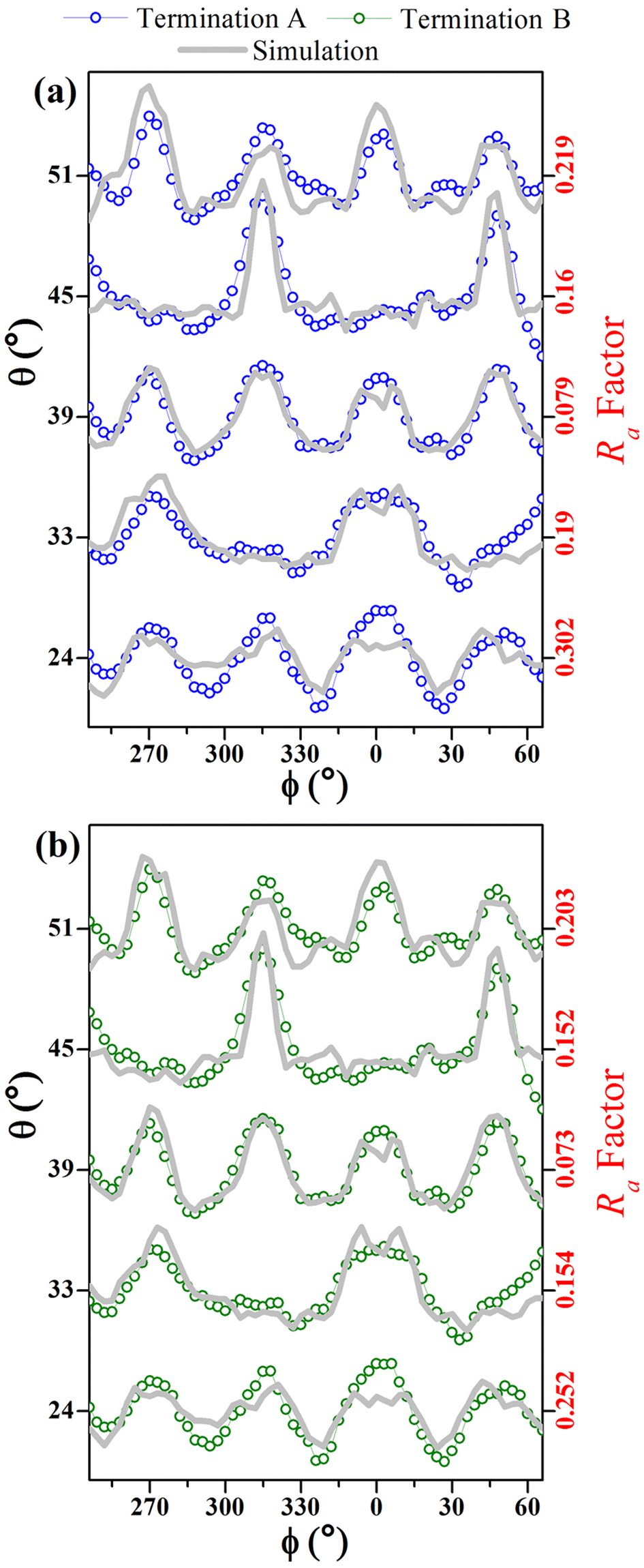 | ||
| Fig. 7 Simulated (gray lines) and experimental (open points) azimuthal scans for selected polar angles (for θ = 24°, 33°, 39°, 45°, and 51°) for (a) termination A (blue open points), and (b) termination B (green open points) model structure surface for O as emitter atom from β-Ga2O3(100) surface. | ||
Of the terminations studied in these simulations have global Ra-factors below 0.23, which is not sufficiently different for distinguishing between the terminations, even though they are clearly consistent with the β-Ga2O3(100) structure. Since the experiment in Fig. 4(a) involves polar angles from 18° to 54°, the small polar angle data (≤39°), which reflect internal layers, mask those for the more grazing angles, which are surface sensitive. In order to demonstrate this, we show, in Fig. 7(a and b), the Ra-factor for the higher (i.e., more grazing) polar angles (≥39°) calculated by summing over the azimuthal intensities for each polar angle. The different curves are labeled according to our termination nomenclature, as in Fig. 1. From Fig. 7, it is very clear that this more surface sensitive data allows us to distinguish between the different termination models. With this additional information it appears that the surface is most likely B terminated.
The simulated XPD patterns for all polar angles (18° to 54°) are shown in Fig. 8(a) for the proposed β-Ga2O3(100)-A surface termination and Fig. 8(b) for β-Ga2O3(100)-B surface termination, where O 1s was used as emitter atom. For these models, we considered all relaxations which yielded Ra factors of 0.228 and 0.204 for A and B terminated surfaces respectively. The study of monoclinic surface structure by XPD simulations is quite a challenging task, since the description of periodicity of layers in the β-Ga2O3 [100] is low, moreover normally the oxide metal and semiconductor materials have defects and vacancies for both anions or cations on the surface.22,23,36,37 Despite the difficulty results in this work showed good agreement between theoretical proposed models and experiment.
 | ||
| Fig. 8 Theoretical XPD patterns obtained from the β-Ga2O3(100) surface models, for termination (a) A and (b) B. | ||
Fig. 9(a) displays the β-Ga2O3 (100)-A surface for the final structural model for termination A. For model A, d12 and d34 and d45 interlayer distances are followed by an expansion and d23 contraction. For model B displayed in the Fig. 9(b), d12 and d45 interlayer distances is observed contraction and expansion for d23 and d34, emerging almost coplanarity for the first three layers due to the displacements in the d12, d23 and d34.
 | ||
| Fig. 9 Interlayer distances calculated for the models with termination (a) A and (b) B proposed to describe the β-Ga2O3(100) surfaces. | ||
Regarding STM study,4,11,38 the observed surface morphology was associated with large and small terraces, with 1.5 Å bigger height for the (100) B termination and another small terrace for the (100) A termination. These experiments are not element specific and cannot differentiate the A or B termination at the surface clearly. This work showed which types of atoms that form each type of termination of the surface of the β-Ga2O3[100].The (100)A surface is terminated with O(II) atoms and (100)B is terminated with both Ga(II), O(I), and O(III) atoms. Theoretical studies show the most energetically favorable termination at the β-Ga2O3 (100) surface is the termination (100)B, mainly because the Ga–O are strong covalent bonds at (100)B termination.3,10
Therefore, the knowledge of the structural parameters for the β-Ga2O3 (100) surface at the atomic level is key for understanding electronic properties previously observed in the theoretical studies on to β-Ga2O3 (100) surface. Further investigations considering the results obtained here may enlighten other special phenomena such as ferromagnetism.
Conclusions
A systematic and precise in situ XPD study of the β-Ga2O3 (100) surface was presented here. The LEED and XPS characterization indicated well-ordered surface structures. XPD and structural information was provided by simulations for the model's systems A and B type terminations. The linear combination for B and A termination indicate that the surface termination is 100% predominance of B termination. Model A and B present significant displacements in the interlayer distances of the outermost Ga2O3 (100) in comparison to the bulk value.Moreover, MSCD simulations indicated the formation of almost coplanarity of layers in the proposed model B. The low Ra factor provides the reliability of the results for the two models but the little difference in the Ra factor does not allow the choice of a specific model (A or B) to describe the predominance in the surface. The determination of the distances between atomic planes of the two models proposed here in this work allows knowing and controlling the surface structure, and this raises the opportunity to modify the physical properties of these nanomaterials, in comparison with the bulk structure. The optimized XPD simulations of the surface structure lead to average Ra-factor of 0.204, implying a good agreement between experimental results and simulations. Properties such as thermal and electrical conductivity are strongly influenced by the geometric parameters of these materials and these properties are essential for the manufacture of electronic devices.
Author contributions
Alex Sandre Kilian: writing – original draft, methodology, formal analysis, software, investigation and visualization. Abner de Siervo: methodology, writing – review & editing, resources and software. Guilherme Jean P. Abreu: investigation, writing – review & editing, methodology. Mayron Silva Castro: investigation, editing, and methodology. Tyson Back: methodology, writing – review & editing, resources and software. Alexandre Pancotti: project administration, writing–review & editing, and funding acquisition.Conflicts of interest
There are no conflicts to declare.Acknowledgements
A. S. K. thanks USA Air Force for the resource and his PostDoc fellowship. We would like to acknowledge Dr Ali Sayir for useful discussions. This material is based upon work supported by the Air Force Office of Scientific Research (AFOSR) under award FA9550-21-1-0440 and Conselho Nacional de Desenvolvimento Científico e Tecnológico – CNPq programme 310774/2020-9 under grant agreement.Notes and references
- S. Roy, A. Bhattacharyya, P. Ranga, H. Splawn, J. Leach and S. Krishnamoorthy, IEEE Electron Device Lett., 2021, 42, 1140–1143 CAS.
- J. Zhang, J. Shi, D.-C. Qi, L. Chen and K. H. L. Zhang, APL Mater., 2020, 8, 020906 CrossRef CAS.
- D. Guo, Q. Guo, Z. Chen, Z. Wu, P. Li and W. Tang, Mater. Today Phys., 2019, 11, 100157 CrossRef.
- H. Xue, Q. He, G. Jian, S. Long, T. Pang and M. Liu, Nanoscale Res. Lett., 2018, 13, 290 CrossRef PubMed.
- V. M. Bermudez, Chem. Phys., 2006, 323, 193–203 CrossRef CAS.
- B. R. Tak, S. Kumar, A. K. Kapoor, D. Wang, X. Li, H. Sun and R. Singh, J. Phys. D: Appl. Phys., 2021, 54, 453002 CrossRef CAS.
- S. Ghose, S. Rahman, L. Hong, J. S. Rojas-Ramirez, H. Jin, K. Park, R. Klie and R. Droopad, J. Appl. Phys., 2017, 122, 095302 CrossRef.
- E. Ahmadi and Y. Oshima, J. Appl. Phys., 2019, 126, 160901 CrossRef.
- S. K. Barman and M. N. Huda, Phys. Status Solidi RRL, 2019, 13, 1800554 CrossRef.
- J. Kim, S. Oh, M. A. Mastro and J. Kim, Phys. Chem. Chem. Phys., 2016, 18, 15760–15764 RSC.
- J. Zhao, X. Wang, H. Chen, Z. Zhang and M. Hua, Chem. Mater., 2022, 34, 3648–3658 CrossRef CAS.
- J. Zhao, X. Huang, Y. Yin, Y. Liao, H. Mo, Q. Qian, Y. Guo, X. Chen, Z. Zhang and M. Hua, J. Phys. Chem. Lett., 2021, 12, 5813–5820 CrossRef CAS PubMed.
- J. Su, R. Guo, Z. Lin, S. Zhang, J. Zhang, J. Chang and Y. Hao, J. Phys. Chem. C, 2018, 122, 24592–24599 CrossRef CAS.
- W. Ding, J. Zhu, Z. Wang, Y. Gao, D. Xiao, Y. Gu, Z. Zhang and W. Zhu, Nat. Commun., 2017, 8, 14956 CrossRef CAS PubMed.
- M. Busch, E. Meyer, K. Irmscher, Z. Galazka, K. Gärtner and H. Winter, Appl. Phys. Lett., 2014, 105, 051603 CrossRef.
- M. Mohamed, I. Unger, C. Janowitz, R. Manzke, Z. Galazka, R. Uecker and R. Fornari, J. Phys.: Conf. Ser., 2011, 286, 012027 CrossRef.
- T. C. Lovejoy, E. N. Yitamben, N. Shamir, J. Morales, E. G. Villora, K. Shimamura, S. Zheng, F. S. Ohuchi and M. A. Olmstead, Appl. Phys. Lett., 2009, 94, 081906 CrossRef.
- P. Mazzolini, A. Falkenstein, C. Wouters, R. Schewski, T. Markurt, Z. Galazka, M. Martin, M. Albrecht and O. Bierwagen, APL Mater., 2020, 8, 011107 CrossRef CAS.
- S. Jang, S. Jung, K. Beers, J. Yang, F. Ren, A. Kuramata, S. J. Pearton and K. H. Baik, J. Alloys Compd., 2018, 731, 118–125 CrossRef CAS.
- A. Pancotti, T. C. Back, W. Hamouda, M. Lachheb, C. Lubin, P. Soukiassian, J. Boeckl, D. Dorsey, S. Mou, T. Asel, G. Geneste and N. Barrett, Phys. Rev. B, 2020, 102, 245306 CrossRef CAS.
- T. Liu, Z. Feng, Q. Li, J. Yang, C. Li and M. Dupuis, Chem. Mater., 2018, 30, 7714–7726 CrossRef CAS.
- A. S. Kilian, G. J. Abreu, A. de Siervo, R. Landers and J. Morais, CrystEngComm, 2022, 24, 2270–2279 RSC.
- A. S. Kilian, F. Bernardi, A. Pancotti, R. Landers, A. de Siervo and J. Morais, J. Phys. Chem. C, 2014, 118, 20452–20460 CrossRef CAS.
- A. S. Kilian, A. Pancotti, R. Landers, A. de Siervo and J. Morais, CrystEngComm, 2014, 16, 9291–9298 RSC.
- Y. Chen, F. J. García de Abajo, A. Chassé, R. X. Ynzunza, A. P. Kaduwela, M. A. Van Hove and C. S. Fadley, Phys. Rev. B: Condens. Matter Mater. Phys., 1998, 58, 13121 CrossRef CAS.
- J. J. Rehr and R. C. Albers, Phys. Rev. B: Condens. Matter Mater. Phys., 1990, 41, 8139–8149 CrossRef PubMed.
- J. B. Pendry, J. Phys. C: Solid State Phys., 1980, 13, 937–944 CrossRef CAS.
- P. Chen, K. Li, B. Lei, L. Chen, W. Cui, Y. Sun, W. Zhang, Y. Zhou and F. Dong, ACS Appl. Mater. Interfaces, 2021, 13, 50975–50987 CrossRef CAS PubMed.
- D. A. Zatsepin, D. W. Boukhvalov, A. F. Zatsepin, Y. A. Kuznetsova, D. Gogova, V. Y. Shur and A. A. Esin, Superlattices Microstruct., 2018, 120, 90–100 CrossRef CAS.
- M. Mulazzi, F. Reichmann, A. Becker, W. M. Klesse, P. Alippi, V. Fiorentini, A. Parisini, M. Bosi and R. Fornari, APL Mater., 2019, 7, 022522 CrossRef.
- Q. Chen, Y. Zhang, T. Zheng, Z. Liu, L. Wu, Z. Wang and J. Li, Nanoscale Adv., 2020, 2, 2705–2712 RSC.
- A. Usseinov, Z. Koishybayeva, A. Platonenko, V. Pankratov, Y. Suchikova, A. Akilbekov, M. Zdorovets, J. Purans and A. I. Popov, Materials, 2021, 14, 7384 CrossRef CAS PubMed.
- J. Su, J. Zhang, R. Guo, Z. Lin, M. Liu, J. Zhang, J. Chang and Y. Hao, Mater. Des., 2019, 184, 108197 CrossRef CAS.
- K. Iwaya, R. Shimizu, H. Aida, T. Hashizume and T. Hitosugi, Appl. Phys. Lett., 2011, 98, 142116 CrossRef.
- E. A. Gonzalez, P. V. Jasen, A. Juan, S. E. Collins, M. A. Baltanás and A. L. Bonivardi, Surf. Sci., 2005, 575, 171–180 CrossRef CAS.
- G. J. P. Abreu, A. Pancotti, L. H. Lima, R. Landers and A. Siervo, J. Nanopart. Res., 2013, 15, 1–10 CrossRef.
- A. Pancotti, A. de Siervo, M. Carazzolle, R. Landers and G. Kleiman, Top. Catal., 2011, 54, 90–96 CrossRef CAS.
- B. Anam and N. Gaston, ChemPhysChem, 2021, 22, 2362–2370 CrossRef CAS PubMed.
| This journal is © The Royal Society of Chemistry 2023 |