
 Open Access Article
 This Open Access Article is licensed under a Creative Commons Attribution-Non Commercial 3.0 Unported Licence
Engineering electronic structures and optical properties of a MoSi2N4 monolayer via modulating surface hydrogen chemisorption†
Yumei Zhanga,
Shunhong Donga,
Pachaiyappan Murugana,
Ting Zhu ab,
Chen Qinga,
Zhiyong Liu*ab,
Weibin Zhang*ab and
Hong-En Wang*ab
ab,
Chen Qinga,
Zhiyong Liu*ab,
Weibin Zhang*ab and
Hong-En Wang*ab
aYunnan Key Laboratory of Optoelectronic Information Technology, College of Physics and Electronic Information, Yunnan Normal University, Kunming 650500, China. E-mail: liuzhiyong@ynnu.edu.cn; 220001@ynnu.edu.cn; hongen.wang@outlook.com
bKey Laboratory of Advanced Technique & Preparation for Renewable Energy Materials, Ministry of Education, Yunnan Normal University, China
First published on 4th September 2023
Abstract
Recently, a MoSi2N4 monolayer has been successfully synthesized by a delicately designed chemical vapor deposition (CVD) method. It exhibits promising (opto)electronic properties due to a relatively narrow bandgap (∼1.94 eV), high electron/hole mobility, and excellent thermal/chemical stability. Currently, much effort is being devoted to further improving its properties through engineering defects or constructing nanocomposites (e.g., van der Waals heterostructures). Herein, we report a theoretical investigation on hydrogenation as an alternative surface functionalization approach to effectively manipulate its electronic structures and optical properties. The calculation results suggested that chemisorption of H atoms on the top of N atoms on MoSi2N4 was energetically most favored. Upon H chemisorption, the band gap values gradually decreased from 1.89 eV (for intrinsic MoSi2N4) to 0 eV (for MoSi2N4-16H) and 0.25 eV (for MoSi2N4-32H), respectively. The results of optical properties studies revealed that a noticeable enhancement in light absorption intensity could be realized in the visible light range after the surface hydrogenation process. Specifically, full-hydrogenated MoSi2N4 (MoSi2N4-32H) manifested a higher absorption coefficient than that of semi-hydrogenated MoSi2N4 (MoSi2N4-16H) in the visible light range. This work can provide theoretical guidance for rational engineering of optical and optoelectronic properties of MoSi2N4 monolayer materials via surface hydrogenation towards emerging applications in electronics, optoelectronics, photocatalysis, etc.
1. Introduction
In the past two decades, two-dimensional (2D) nanomaterials1–3 have attracted enormous attention due to their unique physical and chemical properties, such as high surface area, fast migration of photo-induced electrons and holes to the reaction interface/front, high charge carrier separation efficiency, superior electronic and optical properties and rich reaction sites. Particularly, identification of two-dimensional layered materials in the monolayer limit can lead to the discovering of some new phenomena and unusual properties. Thus, researchers have continuously explored new 2D (monolayer) nanomaterials through experimental and theoretical investigations for various emerging applications in photoelectric and energy-intensive fields.Recently, Ren's group successfully synthesized a new monolayered MoSi2N4 material via a modified chemical vapor deposition (CVD) method.4 The MoSi2N4 monolayer was constructed by septuple atomic layers of Ni–Si–N–Mo–N–Si–N, as viewed as a MoN2 layer sandwiched between two Si–N bilayers.5 It displayed a bandgap of ∼1.94 eV with a high mechanical strength and excellent chemical stability in atmosphere. These properties endowed MoSi2N4 with promising applications in electronic/optoelectronic devices, optical sensors, and photocatalysis.
The great application potential of MoSi2N4 monolayer material has spurred increasing interest in further improving its properties by constructing various (van der Waals) heterostructures. For example, Ang et al. reported tunable electronic properties and band alignments in MoSi2N4/GaN and MoSi2N4/ZnO van der Waals heterostructures.6 Nguyen et al. studied the effects of interlayer coupling and under electric fields on the electronic structures of type-II C3N4/MoSi2N4 heterostructure.7 In addition, two-dimensional metal/semiconductor contact in a Janus MoSH/MoSi2N4 van der Waals heterostructure8 and MoSi2N4/MoS2 van der Waals heterostructure with good optoelectronic performance and tunable electronic properties9 were investigated. Apart from heterostructure engineering, Cui et al. found that metal atoms-adsorbed MoSi2N4 (ref. 10) systems could enable the manufacture of spintronic and vacuum field emission nanodevices. Luo et al. used first principles calculations to study the structural and electronic properties of organic molecules-doped MoSi2N4 monolayers,11 demonstrating the importance of molecular doping in tuning the electronic properties of MoSi2N4 with extended applications.
Heterostructure engineering,12,13 adsorption and substitutional doping14–19 have been proven to be effective ways to modify various properties of semiconductor materials. In addition, surface functionalization,20–24 such as fluoridation and hydrogenation, can also be used to manipulate the properties of 2D materials. Recently, Binh et al. applied the hydrogenation method to change the properties of GeC,25 and InN26 monolayers, largely extending the applications of these materials. Chen et al. demonstrated that the fluorinated MoSi2N4 monolayer27 may exhibit a variety of properties and have the potential to fabricate novel optoelectronic devices by simply adjusting the degree of fluorination. Given the structure similarity between GeC/InN and MoSi2N4, hydrogenation could be a simple, clean, yet effective approach to engineer the electronic and optical properties of MoSi2N4 monolayers and expand its applications.
In this work, we performed a comprehensive first-principles density functional theory study on the hydrogenation of MoSi2N4 monolayer. The calculations reveal that the hydrogenated MoSi2N4 monolayers are thermodynamically stable. Meantime, electronic structures and optical properties of hydrogenated MoSi2N4 can be well regulated as a function of hydrogenation degree on the MoSi2N4 surface. The simulation results suggest that the hydrogenated MoSi2N4 monolayers can have promising applications in photocatalysis28 and other clean energy-related fields.
2. Computational details
First-principles calculations based on quantum mechanics29 can provide a reliable means to investigate the behavior of electrons and nuclei under specific circumstances. In current work, the electronic structure30 and optical properties of both the pristine and hydrogenated MoSi2N4 monolayers were studied. Based on density functional theory (DFT)31,32 and plane-wave pseudo-potential basis, a collection of analytical tools within Cambridge Sequential Total Energy Package (CASTEP),33 was used for first principles34,35 calculations. The exchange correlation functional was represented by generalized gradient approximation (GGA) of the Perdew–Burke–Ernzerhof (PBE) functional.36 The semi-empirical DFT-D2 method of Grimmes correctly considers the weak van der Waals interaction in the material. Because the local density approximation37 (LDA) generally underestimate the equilibrium atomic distances while overestimate the adsorption energy of the model system, and PBE/GGA can provide more precise estimations for geometric optimization. Therefore, the PBE/GGA were applied for geometry optimization and electronic property calculations. The cutoff energy is set as 500 eV. For both electronic and optical analyses, the convergence criterion for the self-consistent electronic loop was set to 2 × 10⁻⁶ eV. Simultaneously, in the Brillouin zone, the 3 × 3 × 1 k-point grid is implemented for calculations. The adsorption energy38 for one H atom adsorbed onto the MoSi2N4 monolayer of Mo, Si, or N atom can be confirmed as| Eads = (Esuf + EH) − EH-suf | (1) |
The investigation focused on the thermodynamic stability of hydrogenated MoSi2N4 through the computation of the formation energy (Ef) using the following equation:
| Ef = (EMoSi2N4-H − mEMo − nESi − lEN − kEH)/(m + n + l + k) | (2) |
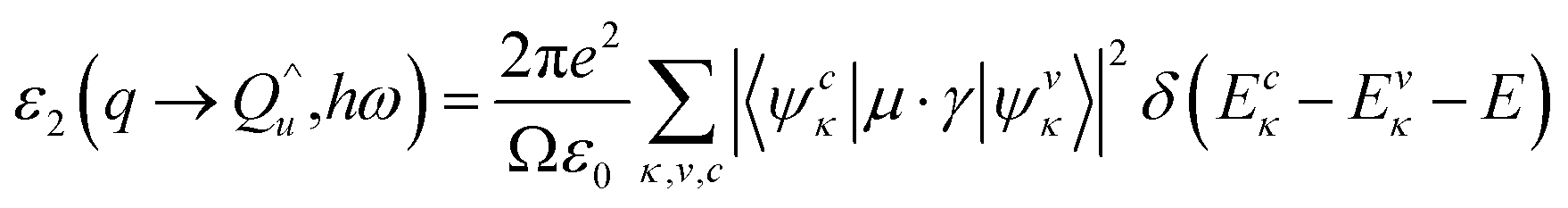
From a quantum mechanical point of standpoint, the interaction between photons and electrons in the system is illustrated by time-dependent perturbations in the ground state, where the absorption or emission of photons causes transition between unoccupied and occupied states. The spectrum produced by excitation can be regarded as a joint density of state (DOS) between the conduction bands (CB) and the valence bands (VB). The imaginary part of the dielectric function ε2(ω) is a function of the photon frequency and can be described as follows:
 | (3) |
 | (4) |
 | (5) |
 | (6) |
3. Results and discussion
3.1. Geometric structure of MoSi2N4-nH monolayers
Fig. 1a and b show top- and side-views of the optimized geometry structure of pristine MoSi2N4 monolayer with the 4 × 4 × 1 supercell. The MoSi2N4 monolayer has a hexagonal crystal symmetry with optimized lattice parameters of a = 2.94 Å and c = 20.31 Å. It has a sandwiched structure consisted of two N–Si–N layers with a Mo layer in the middle.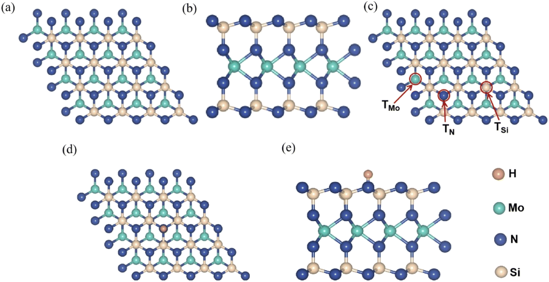 | ||
| Fig. 1 (a) and (b) top- and side-views of pristine MoSi2N4 monolayer; (c) top view showing the different sites for chemisorption of an H atom on a MoSi2N4 monolayer (TMo, TSi, and TN represent the site atop Mo, Si, and N atoms, respectively); (d) top- and (e) side-view of a MoSi2N4 monolayer after chemisorption of an H (MoSi2N4-1H). | ||
Next, the surface sites for H chemisorption were considered. Three different sites was computed for comparison to determine the most stable site for H chemisorption on MoSi2N4 monolayer. Fig. 1c illustrates the chemisorption of an H on three different sites of MoSi2N4 monolayer, referring to atop Mo, Si, and N atoms as defined as TMo, TSi, and TN, respectively. Fig. 1d and e depicts top- and side-views of an H adsorbed on atop of N in MoSi2N4 monolayer (MoSi2N4-1H), with the H atom adsorbed on top of an N atom.
The calculated adsorption energies of an H atop of TMo, TSi and TN are −0.275, −0.948 and −1.601 eV, respectively. The negative adsorption energies suggest that the chemisorption of H on the three sites of the MoSi2N4 monolayer is exothermic and thermodynamically stable. Meanwhile, the lowest adsorption energy is −1.601 eV on TN site indicates it is the most stable adsorption position. Therefore, the following discussion focuses mainly on the chemisorption of different H atoms on TN sites. The maximum number of H atoms adsorbed at TN sites on one side of MoSi2N4 monolayer can be estimated as 16 based on supercell size.
Then, the calculated formation energy (Ef) for hydrogenated MoSi2N4 was investigated to confirm the stability of hydrogenated MoSi2N4 further. As shown in Table 1 and Fig. S1 (ESI†), with the number of H increase, the formation energy are slightly increased because of the repulse interaction increase between the H atoms. However, the formation energy of different number of H chemisorption on the MoSi2N4 systems are all negative, indicating the stability of the systems. This result implies the occurrence of a favorable exothermic reaction between the MoSi2N4 monolayer and the H atom, highlighting the overall chemical stability of the structure.
| Ef (eV) | |
|---|---|
| MoSi2N4-1H | −1.890 |
| MoSi2N4-2H | −1.864 |
| MoSi2N4-4H | −1.823 |
| MoSi2N4-6H | −1.766 |
| MoSi2N4-8H | −1.742 |
| MoSi2N4-10H | −1.712 |
| MoSi2N4-12H | −1.683 |
| MoSi2N4-14H | −1.635 |
| MoSi2N4-16H | −1.608 |
| MoSi2N4-32H | −1.247 |
Fig. 2 shows top and side view of MoSi2N4-nH, n is the number of H atoms adsorbed on the surface. As the number of H atoms increases, the resulting MoSi2N4-nH retains the sandwich structure. As shown in Fig. 2d, when four H atoms are adsorbed, an adsorption energy is −1.69 eV can be derived, which comparable to that of MoSi2N4-1H (−1.60 eV). As the number of adsorbed H atoms increases, the corresponding adsorption energy gradually becomes more negative (e.g., −1.99 eV for MoSi2N4-16H). This situation illustrate that the monolayer structures remain stable with increased H atoms.
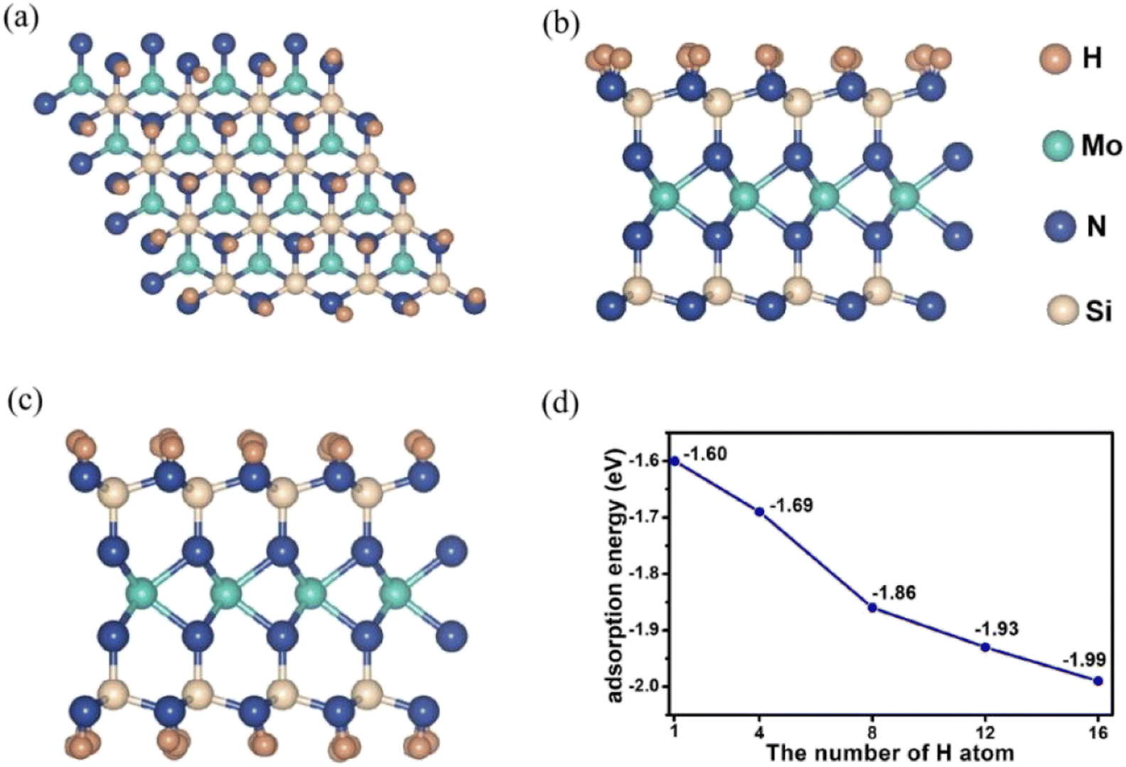 | ||
| Fig. 2 (a) Top view of MoSi2N4-16H, (b) and (c) side view of MoSi2N4-16H and MoSi2N4-32H, (d) trend in the adsorption energies of MoSi2N4-nH (n = 1, 4, 8, 12, and 16). | ||
3.2. Electronic properties of MoSi2N4-nH monolayers
The effects of adsorbed H on the electronics structures of MoSi2N4-nH were next investigated by band structure (BS) and density of state (DOS) calculations. Fig. 3 shows the calculation results of BS and DOS of pristine MoSi2N4 monolayer. The labels G, F, and H represent high-symmetry points in the Brillouin zone with fractional coordinates of G (0, 0, 0), F (0, 0.5, 0), and H (−0.333, 0.667, 0.5), respectively. The valence band maximum42 (VBM) and conduction band minimum43 (CBM) are located at the different positions in the G and H points of Brillouin zone, illustrating that pristine MoSi2N4 is an indirect band gap semiconductor. Fig. 3a exhibits the BS of pristine MoSi2N4. The calculated band gap is 1.89 eV, near to the experimental value of 1.94 eV.44 Fig. 3b shows the computed DOS of pristine MoSi2N4 monolayer. The valence band edge45 (VBE) in the range of −3 to 0 eV energy level was primarily contributed by the Mo 4d and N 2p state. The conduction band edge (CBE) from 2 to 3 eV is mainly contributed by the Si 3p, Mo 4d and N 2p states.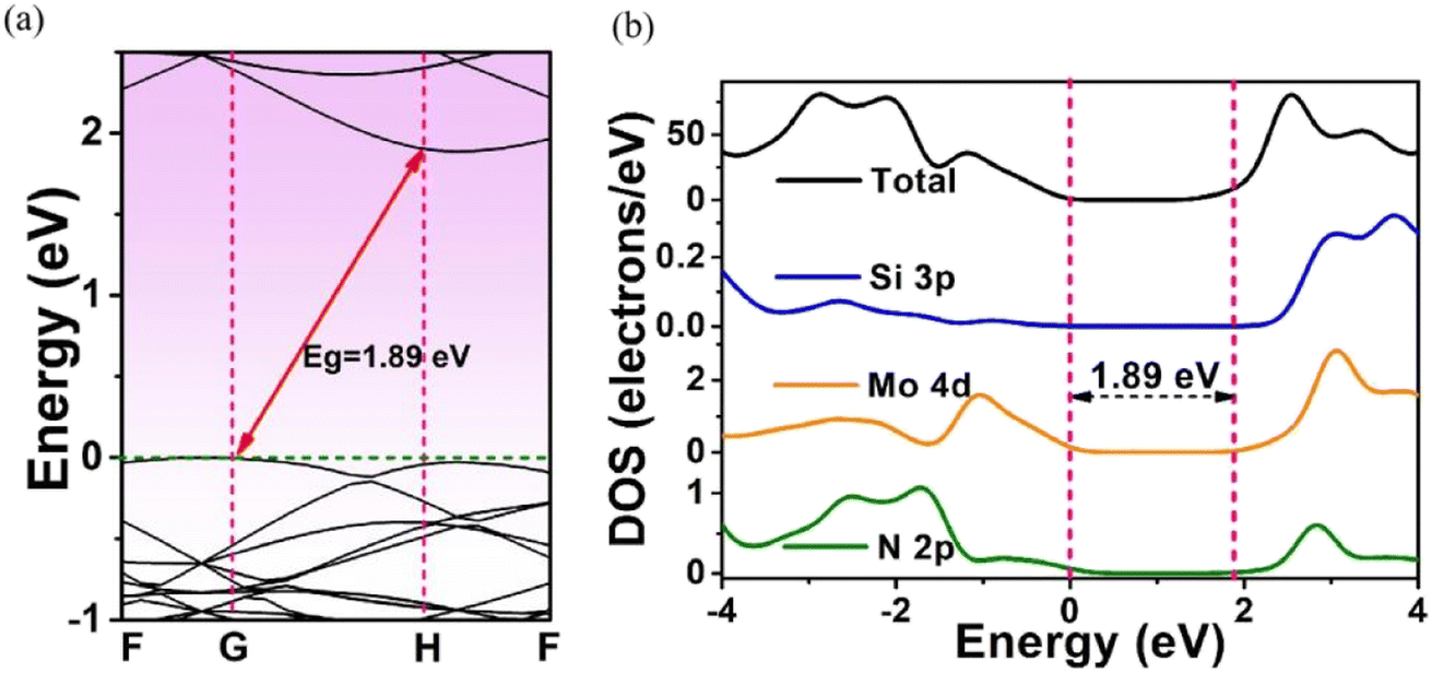 | ||
| Fig. 3 (a) Energy band structure and (b) density of states (DOS) plots of a pristine MoSi2N4 monolayer. The Fermi level is set at 0 eV. | ||
Fig. 4 shows the calculated BS and DOS profiles of MoSi2N4-8H monolayer. Its band gap was 0.98 eV, less than that of pristine MoSi2N4. From DOS plot (Fig. 4b), its VBE in the energy range from −4 to 0 eV was primarily composed of Mo 4d and Si 3p state and CBE in the energy range from 1 to 4 eV was mainly comprised of Si 3p, Mo 4d, and H 1s state.
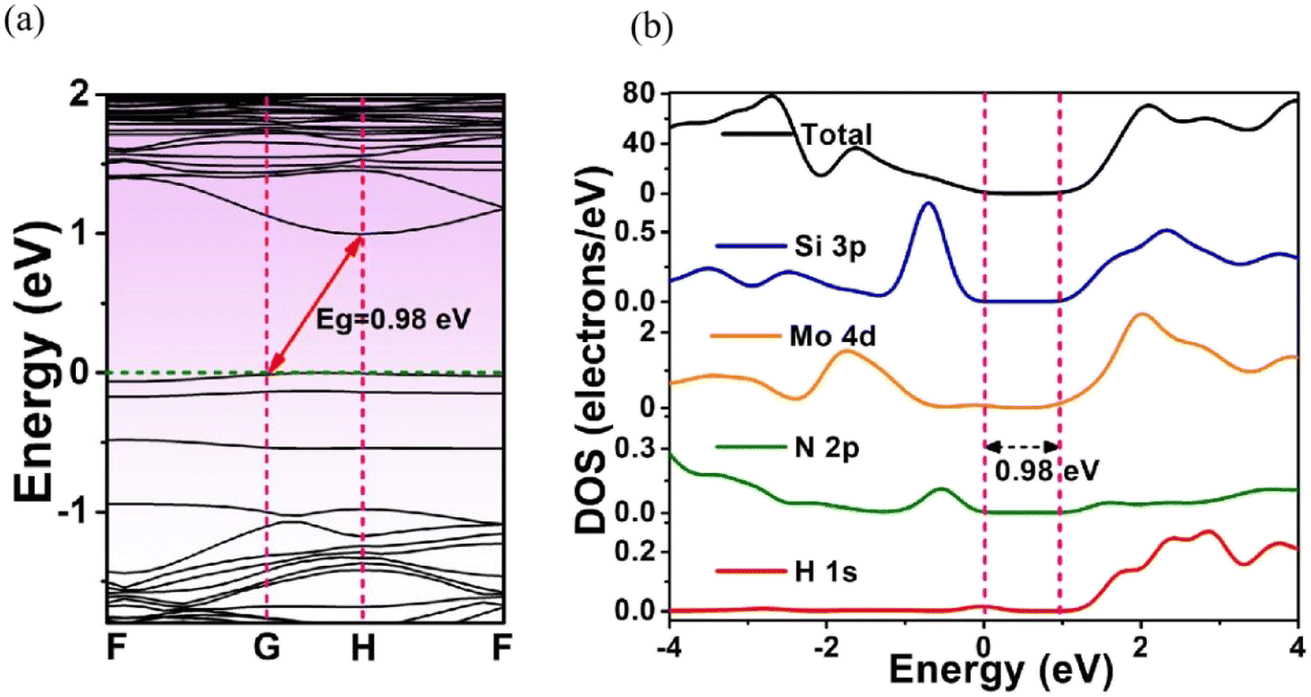 | ||
| Fig. 4 (a) Energy band structure and (b) DOS of MoSi2N4-8H monolayer. The Fermi level is set at 0 eV. | ||
The band structures of the H-adsorbed MoSi2N4 monolayer are shown in Fig. 5. From Fig. 5a and b, the MoSi2N4-1H and MoSi2N4-16H monolayers are both indirect semiconductors with calculated band gap values of 1.88 and 0 eV, respectively. Also, the phenomenon exhibits an indirect band gap for H-adsorbed MoSi2N4. Fig. 5c shows the band gap of the MoSi2N4-nH as a function of the number of H atoms (“n”) adsorbed on MoSi2N4 monolayer. It is evident that the band gap of MoSi2N4-nH continuously decreases as the surface-adsorbed H atom increases possibly with an increased impurity level. The decreased band gap of the MoSi2N4-nH monolayer suggests its optical absorption can be extended to the visible and infrared regions properties. This enables its promising application as a potential photocatalytic material clean energy conversion and utilization.
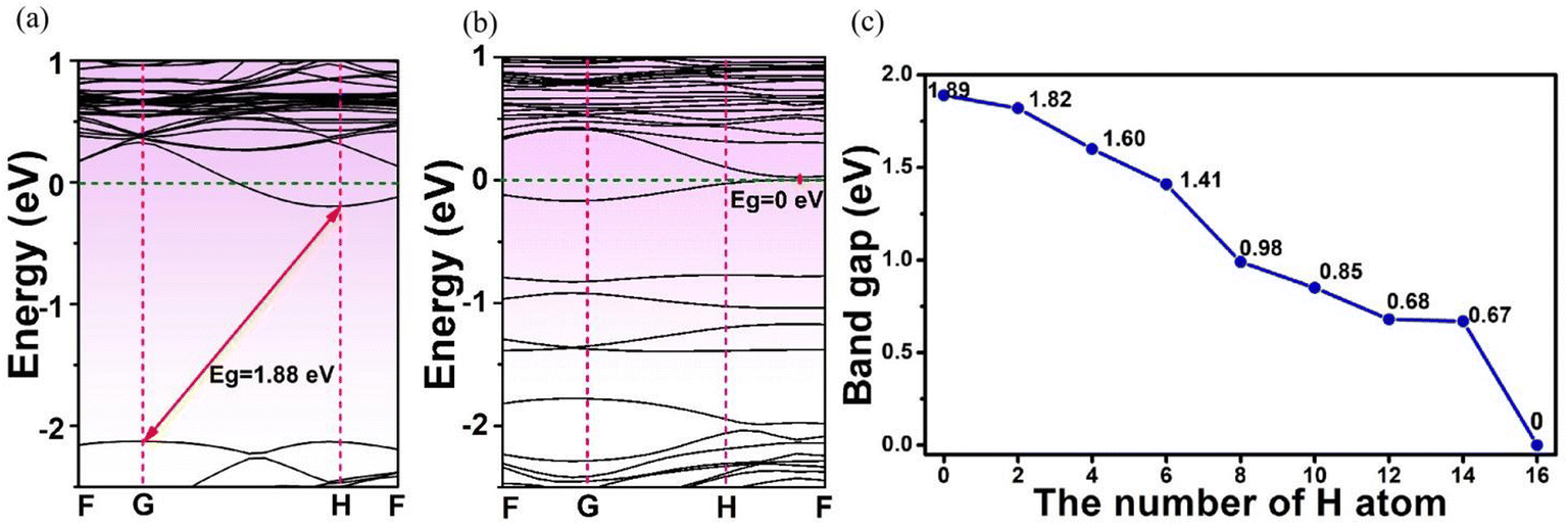 | ||
| Fig. 5 Energy band structures of (a) MoSi2N4-1H and (b) MoSi2N4-16H; and (c) band gap of MoSi2N4-nH monolayer (n = 0, 2, 4, 6, 8, 10, 12, 14 and 16). MoSi2N4-nH denotes a MoSi2N4 monolayer after chemisorption of “n” H atoms. | ||
3.3. Optical property variation of MoSi2N4-nH monolayers
The dielectric function of MoSi2N4-nH (n = 0, 1, 8 and 16) monolayers is calculated to evaluate the influence of electronic structure change on its optical properties (Fig. 6). Fig. 6a demonstrates the real part ε1(ω) of pristine and nH-adsorbed MoSi2N4 monolayer systems. The pristine MoSi2N4 monolayer exhibits a dielectric constant ε1(0) of 5.1. For H atom-adsorbed MoSi2N4 monolayer, the ε1(0) are 4.8 (1H-chemisorption), 5.5 (4H-chemisorption) and 10.9 (16H-chemisorption), respectively. The result illustrates that ε1(0) of the nH-adsorbed systems is significantly larger than that of the system without adsorbed hydrogen, except that of MoSi2N4-1H monolayer possibly due to the occasional calculation error.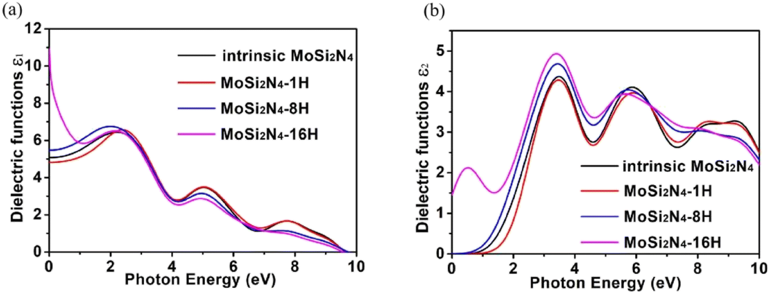 | ||
| Fig. 6 Dielectric functions of the pristine MoSi2N4 and MoSi2N4-nH (n = 0, 1, 8 and 16) monolayers: (a) real part; (b) imaginary part. | ||
A higher dielectric constant can lead to a stronger ability to bind electrons and a less polarization. Therefore, with the increase of H atom chemisorption, the polarization intensity decreases and the thermal stability of MoSi2N4-nH system increases. Fig. 6b shows the imaginary parts of the dielectric functions. For pristine MoSi2N4, it can be seen that the imaginary part has three main peaks at 3.4, 6.1, and 9.1 eV, corresponding to the three intrinsic plasma frequencies. By analyzing the electronic band structure, we speculate that the peak at 3.4 eV may be caused by the electron transition between the N 2p state and the Mo 4d state in the conduction band minimum. The peaks at 6.1 and 9.1 eV may result from electronic transitions between the N 2p, Mo 4d and Si 3p states. It can also be seen that the line shapes of MoSi2N4-nH monolayers are almost the same in all energy ranges, and the peaks of MoSi2N4-16H monolayer at 3.4, 6.1 and 9.1 eV are consistent with the peaks of MoSi2N4-nH monolayer, but a weak peak is noted at 0.5 eV. However, the MoSi2N4-16H monolayer exhibits a distinctly different peak shape in the 0–2 eV range. In the high energy range, the line shapes of MoSi2N4-nH (n = 0, 1 and 8), these observations indicate that the difference in the number of H atoms adsorbed mainly affect the optical properties in the low energy zone.
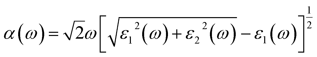
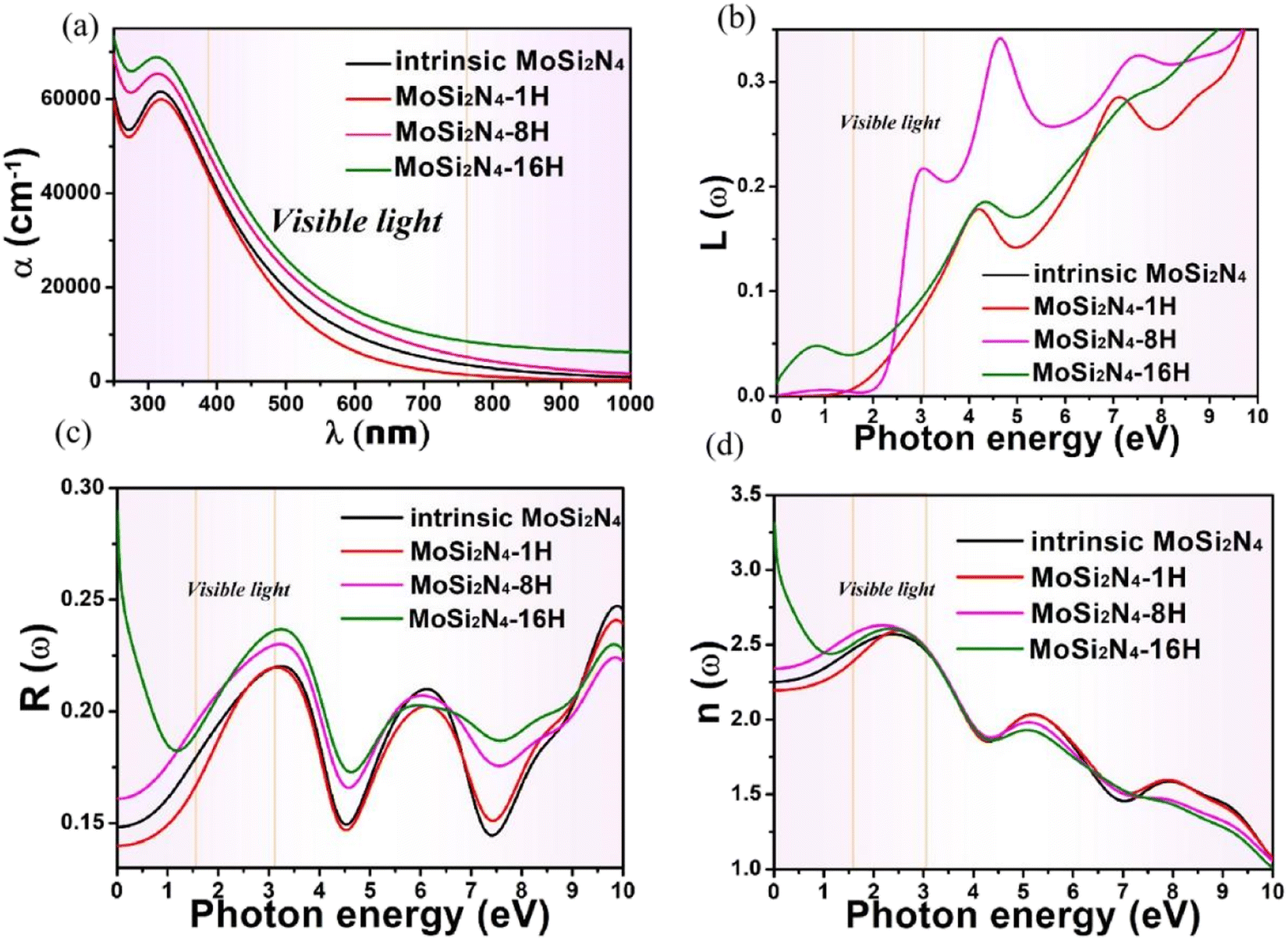
The absorption coefficients α(ω) of the intrinsic and H-decorated MoSi2N4 monolayers were calculated using the obtained ε1(ω) and ε2(ω). Fig. 7a shows the absorption spectra of pristine MoSi2N4 and MoSi2N4-nH monolayer. As can be seen from the figure, the absorption region becomes significantly wider after chemisorption of H, and the absorption coefficient in the visible region is greatly improved compared with the pristine MoSi2N4. It suggests that H chemisorption is favorable for photocatalytic activity, making MoSi2N4-nH a potential candidate for photoelectrochemical applications.
 | ||
| Fig. 7 (a) Absorption spectra, (b) energy loss function plots, (c) reflectivity spectra, and (d) refractivity index spectra for MoSi2N4 and MoSi2N4-nH (n = 0, 1, 8 and 16). The pink areas indicate the visible light region. | ||
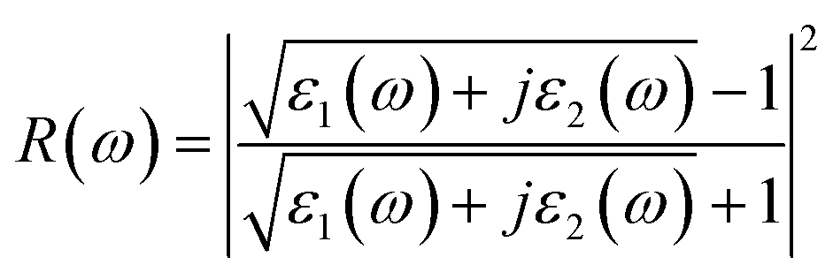
Fig. 7b–d shows the energy-loss spectrum, that is, the reflectivity (R(ω)) and the refractive indices (n(ω)) of MoSi2N4-nH monolayers in the range of 0–10 eV. Fig. 7b exhibits the energy loss plots, where the spike near 4.2 eV can be attributed to plasma oscillations. It is worth mentioning that the peak in the energy loss spectrum corresponds to the valleys in the reflection spectrum. It can be seen from Fig. 7c that the reflectivity drops suddenly at about 4.3 eV and keeps the same trend as the peak value of the energy loss spectrum. In the light energy range from 1.8–3.5 eV, MoSi2N4-nH shows reflectivity peaks at 3.5 eV and refractivity peaks at 2.6 eV. The results show that H-adsorbed MoSi2N4 has a higher refractive index and substantially unchanged reflectance in visible region.
3.4. The electronic and optical properties of semi and full-hydrogenated MoSi2N4
The work function is defined as the minimum energy for an electron escaping from the surface as can be calculated by the following equation:| Φ = E0 − EF | (7) |
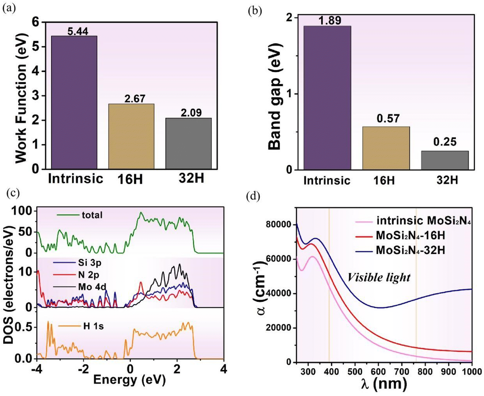 | ||
| Fig. 8 (a) The change of work function Φ for H adsorbed MoSi2N4 systems, (b) the band gap of MoSi2N4-nH (n = 0 and 32), (c) density of state of 32H-adsorbed MoSi2N4 monolayer, (d) absorption spectra of MoSi2N4-nH (n = 0, 16 and 32). | ||
Fig. 8b shows the band gap variations of pristine and full-hydrogenated MoSi2N4 systems. With the increase of the hydrogenation degree, the band gap of MoSi2N4 monolayer system decreases continuously. The result shows that the band gap of pristine MoSi2N4 is 1.89 eV and the full-hydrogenated MoSi2N4 is 0.25 eV. In combination with Fig. 8c, there are two impurity energy levels of Si 3p and N 2p states, and the two states are hybridized to form the impurity band. The impurity energy band of H 1s enters the valence band and is connected with the valence band to form a new degenerated energy band, which leads to the decrease of the gap bandwidth. The above phenomena show that hydrogenation is the main reason for the band gap decrease. Therefore, the hydrogenation can effectively modulate the size of band gap for MoSi2N4.
Based on the electronic property discussions, the optical properties variations of the MoSi2N4 system are discussed. Fig. 8d depicts the absorption spectra of pristine, semi- and full-hydrogenated MoSi2N4, respectively. In the visible range, the absorption coefficients of full-hydrogenated MoSi2N4 monolayers are much larger than those of the other two cases. These results indicate that full-hydrogenated MoSi2N4 monolayer is more suitable for solar cell and photocatalytic applications.
4. Conclusions
In this study, the structural, electronic, and optical properties of H-adsorbed MoSi2N4 monolayers were investigated using first principles calculations. The calculated energy of formation (Ef) for MoSi2N4 hydrogenation was determined to be negative, indicative of thermodynamic stability. This finding suggests the presence of a beneficial exothermic reaction between the MoSi2N4 monolayer and the H atom, emphasizing the overall chemical stability of the structure. Also, the negative adsorption energy indicates the stability of MoSi2N4 monolayer structure adsorbed with H. The electronic structure analysis shows that the pristine MoSi2N4 monolayer is an indirect band gap semiconductor (with a band gap of 1.89 eV). With the increase of H atoms adsorbed on MoSi2N4 monolayer, the band gaps gradually decrease from 1.89 eV to 0 eV (16H-adsorbed) and 0.25 eV (32H-adsorbed), which indicates hydrogenation can effectively change the width of band gap and make MoSi2N4 system into adjustable band-gap structure. The results of work function analysis show that H chemisorption on MoSi2N4 monolayers reduces the work function value, and full-hydrogenated monolayer has a minimum work function, which is conducive to the electron transition application for photocatalysis. The optical study reveals that the chemisorption of H atoms greatly increases the dielectric constant of MoSi2N4. The visible light absorption range and visible light absorption coefficient are also increased. Moreover, compared with semi-hydrogenated chemisorption, the absorption coefficient of full-hydrogenated monolayer in the visible range is much larger. Overall, due to the unique physical and chemical properties, H-adsorbed MoSi2N4 monolayers are promising candidates for novel photocatalytic materials and optoelectronic devices.Conflicts of interest
There are no conflicts to declare.Acknowledgements
This work was supported by the National Natural Science Foundation of China (no. 52262042) and Spring City Plan: The High-level Talent Promotion and Training Project of Kunming (2022SCP005).References
- J. Feng, M. Graf, K. Liu, D. Ovchinnikov, D. Dumcenco, M. Heiranian, V. Nandigana, N. R. Aluru, A. Kis and A. Radenovic, Single-layer MoS2 nanopores as nanopower generators, Nature, 2016, 536, 197–200 CrossRef CAS PubMed.
- H. Li, C. Tsai, A. L. Koh, L. Cai, A. W. Contryman, A. H. Fragapane, J. Zhao, H. S. Han, H. C. Manoharan, F. Abild-Pedersen, J. K. Nørskov and X. Zheng, Activating and optimizing MoS2 basal planes for hydrogen evolution through the formation of strained sulphur vacancies, Nat. Mater., 2016, 15, 48–53 CrossRef CAS PubMed.
- S. B. Desai, S. R. Madhvapathy, A. B. Sachid, J. P. Llinas, Q. X. Wang, G. H. Ahn, G. Pitner, M. J. Kim, J. Bokor, C. M. Hu, H. S. P. Wong and A. Javey, MoS2 transistors with 1-nanometer gate lengths, Science, 2016, 354, 99–102 CrossRef CAS PubMed.
- Y. L. Hong, Z. B. Liu, L. Wang, T. Y. Zhou, W. Ma, C. Xu, S. Feng, L. Chen, M. L. Chen, D. M. Sun, X. Q. Chen, H. M. Cheng and W. C. Ren, Chemical vapor deposition of layered two-dimensional MoSi2N4 materials, Science, 2020, 369, 670 CrossRef CAS PubMed.
- W. Shi, G. Yin, S. Yu, T. Hu, X. Wang and Z. Wang, Atomic precision tailoring of two-dimensional MoSi2N4 as electrocatalyst for hydrogen evolution reaction, J. Mater. Sci., 2022, 57, 18535–18548 CrossRef CAS.
- J. Q. Ng, Q. Wu, L. K. Ang and Y. S. Ang, Tunable electronic properties and band alignments of MoSi2N4/GaN and MoSi2N4/ZnO van der Waals heterostructures, Appl. Phys. Lett., 2022, 120, 103101 CrossRef CAS.
- C. Q. Nguyen, Y. S. Ang, S.-T. Nguyen, N. V. Hoang, N. M. Hung and C. V. Nguyen, Tunable type-II band alignment and electronic structure of C3N4 MoSi2N4 heterostructure: interlayer coupling and electric field, Phys. Rev. B, 2022, 105, 045303 CrossRef CAS.
- C. V. Nguyen, C. Q. Nguyen, S. T. Nguyen, Y. S. Ang and N. V. Hieu, Two-Dimensional Metal/Semiconductor Contact in a Janus MoSH/MoSi2N4 van der Waals Heterostructure, J. Phys. Chem. Lett., 2022, 13, 2576–2582 CrossRef CAS PubMed.
- X. H. Xu, L. Yang, Q. Gao, X. X. Jiang, D. M. Li, B. Cui and D. S. Liu, Type-II MoSi2N4/MoS2 van der Waals Heterostructure with Excellent Optoelectronic Performance and Tunable Electronic Properties, J. Phys. Chem. C, 2023, 127, 7878–7886 CrossRef CAS.
- Z. Cui, K. Yang, K. Ren, S. Zhang and L. Wang, Adsorption of metal atoms on MoSi2N4 monolayer: a first principles study, Mater. Sci. Semicond. Process., 2022, 152, 107072 CrossRef CAS.
- Z. Cui, Y. Luo, J. Yu and Y. Xu, Tuning the electronic properties of MoSi2N4 by molecular doping: a first principles investigation, Phys. E, 2021, 134, 114873 CrossRef CAS.
- A. Castellanos-Gomez, X. Duan, Z. Fei, H. R. Gutierrez, Y. Huang, X. Huang, J. Quereda, Q. Qian, E. Sutter and P. Sutter, Van der Waals heterostructures, Nat. Rev. Methods Primers, 2022, 2, 58 CrossRef CAS.
- W. Zhou, X. Zhou, C. Yang, J. Zhang, L. Wang and Q. Li, Tunable type-II lateral MoSi2N4/WSi2N4 heterostructures for photocatalytic applications, Phys. Chem. Chem. Phys., 2022, 24, 26307–26315 RSC.
- M. L. Sun, Q. Q. Ren, Y. M. Zhao, J. P. Chou, J. Yu and W. C. Tang, Electronic and magnetic properties of 4d series transition metal substituted graphene: a first-principles study, Carbon, 2017, 120, 265–273 CrossRef CAS.
- M. L. Sun, W. C. Tang, Q. Q. Ren, Y. M. Zhao, S. K. Wang, J. Yu, Y. H. Du and Y. T. Hao, Electronic and magnetic behaviors of graphene with 5d series transition metal atom substitutions: a first-principles study, Phys. E, 2016, 80, 142–148 CrossRef CAS.
- Y. Luo, S. K. Wang, S. H. Li, Z. M. Sun, J. Yu, W. C. Tang and M. L. Sun, Transition metal doped puckered arsenene: magnetic properties and potential as a catalyst, Phys. E, 2019, 108, 153–159 CrossRef CAS.
- S. Wang and J. Yu, Magnetic Behaviors of 3d Transition Metal-Doped Silicane: a First-Principle Study, J. Supercond. Novel Magn., 2018, 31, 2789–2795 CrossRef CAS.
- M. Sun, Q. Ren, S. Wang, Y. Zhang, Y. Du, J. Yu and W. Tang, Magnetism in transition-metal-doped germanene: a first-principles study, Comput. Mater. Sci., 2016, 118, 112–116 CrossRef CAS.
- M. Sun, Q. Ren, Y. Zhao, S. Wang, J. Yu and W. Tang, Magnetism in transition metal-substituted germanane: a search for room temperature spintronic devices, J. Appl. Phys., 2016, 119, 143904 CrossRef.
- S. K. Wang, H. Y. Tian, Y. Luo, J. Yu, C. D. Ren, C. L. Sun, Y. J. Xu and M. L. Sun, First-principles calculations of aluminium nitride monolayer with chemical functionalization, Appl. Surf. Sci., 2019, 481, 1549–1553 CrossRef CAS.
- M. Sun, J.-P. Chou, Y. Zhao, J. Yu and W. Tang, Weak C–H⋯F–C hydrogen bonds make a big difference in graphane/fluorographane and fluorographene/fluorographane bilayers, Phys. Chem. Chem. Phys., 2017, 19, 28127–28132 RSC.
- W. Tang, M. Sun, Q. Ren, S. Wang and J. Yu, Halogenated arsenenes as Dirac materials, Appl. Surf. Sci., 2016, 376, 286–289 CrossRef CAS.
- W. Tang, M. Sun, Q. Ren, Y. Zhang, S. Wang and J. Yu, First principles study of silicene symmetrically and asymmetrically functionalized with halogen atoms, RSC Adv., 2016, 6, 95846–95854 RSC.
- M. Sun, Q. Ren, S. Wang, J. Yu and W. Tang, Electronic properties of Janus silicene: new direct band gap semiconductors, J. Phys. D: Appl. Phys., 2016, 49, 445305 CrossRef.
- T. V. Vu, N. T. T. Anh, D. M. Hoat, D. P. Tran, H. D. Tong, H. L. Luong, L. M. Hieu, C. V. Nguyen, H. V. Phuc, N. T. T. Binh and N. N. Hieu, Electronic, optical and photocatalytic properties of fully hydrogenated GeC monolayer, Phys. E, 2020, 117, 113857 CrossRef CAS.
- T. V. Vu, K. D. Pham, T. N. Pham, D. D. Vo, P. T. Dang, C. V. Nguyen, H. V. Phuc, N. T. T. Binh, D. M. Hoat and N. N. Hieu, First-principles prediction of chemically functionalized InN monolayers: electronic and optical properties, RSC Adv., 2020, 10, 10731–10739 RSC.
- R. Chen, D. Chen and W. Zhang, First-principles calculations to investigate stability, electronic and optical properties of fluorinated MoSi2N4 monolayer, Results Phys., 2021, 30, 104864 CrossRef.
- H. Liu, B. Huang, Y. Dai and W. Wei, Characteristic excitonic absorption of MoSi2N4 and WSi2N4 monolayers, J. Phys. D: Appl. Phys., 2023, 56, 405103 CrossRef.
- M. D. Segall, J. D. L. Philip, M. J. Probert, C. J. Pickard, P. J. Hasnip, S. J. Clark and M. C. Payne, First-principles simulation: ideas, illustrations and the CASTEP code, J. Phys.: Condens. Matter, 2002, 14, 2717 CrossRef CAS.
- H. G. Si, Y. X. Wang, Y. L. Yan and G. B. Zhang, Structural, Electronic, and Thermoelectric Properties of InSe Nanotubes: First-Principles Calculations, J. Phys. Chem. C, 2012, 116, 3956–3961 CrossRef CAS.
- Y. Xiao, C. Shen and W. B. Zhang, Screening and prediction of metal-doped α-borophene monolayer for nitric oxide elimination, Mater. Today Chem., 2022, 25, 100958 CrossRef CAS.
- C. Zhang, F. Wei, X. Zhang, W. Chen, C. Chen, J. Hao and B. Jia, Thermoelectric properties of monolayer MoSi2N4 and MoGe2N4 with large Seebeck coefficient and high carrier mobility: a first principles study, J. Solid State Chem., 2022, 315, 123447 CrossRef CAS.
- W. Zhang, W. Yang, Y. Liu, Z. Liu and F. Zhang, Computational exploration and screening of novel Janus MA2Z4 (M = Sc–Zn, Y–Ag, Hf–Au; A = Si, Ge; Z = N, P) monolayers and potential application as a photocatalyst, Front. Phys., 2022, 17, 63509 CrossRef.
- R. S. Uwanyuze, S. P. Alpay, S. Schaffoner and S. Sahoo, A first principles analysis of oxidation in titanium alloys with aluminum and vanadium, Surf. Sci., 2022, 719, 122026 CrossRef CAS.
- C. Rebolledo Espinoza, D. A. Ryndyk, A. Dianat, R. Gutierrez and G. Cuniberti, First principles study of field effect device through van der Waals and lateral heterostructures of graphene, phosphorene and graphane, Nano Mater. Sci., 2022, 4, 52–59 CrossRef CAS.
- N. Mwankemwa, H.-E. Wang, T. Zhu, Q. Fan, F. Zhang and W. Zhang, First principles calculations investigation of optoelectronic properties and photocatalytic CO2 reduction of (MoSi2N4)5−n/(MoSiGeN4)n in-plane heterostructures, Results Phys., 2022, 37, 105549 CrossRef.
- M. T. Entwistle, M. J. P. Hodgson, J. Wetherell, B. Longstaff, J. D. Ramsden and R. W. Godby, Local density approximations from finite systems, Phys. Rev. B, 2016, 94, 205134 CrossRef.
- J. C. Tracy, Structural Influences on Adsorption Energy. II. CO on Ni(100), J. Chem. Phys., 2003, 56, 2736–2747 CrossRef.
- A.-M. Hu, L.-L. Wang, W.-Z. Xiao and B. Meng, Electronic structures and magnetic properties in Cu-doped two-dimensional dichalcogenides, Phys. E, 2015, 73, 69–75 CrossRef CAS.
- H. Belhadj, M. Ameri, B. Abbar, N. Moulay, A. Z. Bouyakoub, O. Arbouche, D. Bensaid, I. Ameri, S. Mesbah and Y. Al-Douri, Optical properties of (Pb1−xMnxS)1−y Fey materials from first-principles calculations, Chin. J. Phys., 2017, 55, 1032–1043 CrossRef CAS.
- K. Boudiaf, A. Bouhemadou, O. Boudrifa, K. Haddadi, F. S. Saoud, R. Khenata, Y. Al-Douri, S. Bin-Omran and M. A. Ghebouli, Structural, Elastic, Electronic and Optical Properties of LaOAgS-Type Silver Fluoride Chalcogenides: First-Principles Study, J. Electron. Mater., 2017, 46, 4539–4556 CrossRef CAS.
- S.-C. Liu, C.-M. Dai, Y. Min, Y. Hou, A. H. Proppe, Y. Zhou, C. Chen, S. Chen, J. Tang, D.-J. Xue, E. H. Sargent and J.-S. Hu, An antibonding valence band maximum enables defect-tolerant and stable GeSe photovoltaics, Nat. Commun., 2021, 12, 670 CrossRef CAS PubMed.
- H. Mizoguchi, S.-W. Park, T. Katase, J. Yu, J. Wang and H. Hosono, Unique Conduction Band Minimum of Semiconductors Possessing a Zincblende-Type Framework, Inorg. Chem., 2022, 61, 10359–10364 CrossRef CAS PubMed.
- J. Yu, J. Zhou, X. Wan and Q. Li, High intrinsic lattice thermal conductivity in monolayer MoSi2N4, New J. Phys., 2021, 23, 033005 CrossRef CAS.
- D. J. Trainer, A. V. Putilov, C. Di Giorgio, T. Saari, B. K. Wang, M. Wolak, R. U. Chandrasena, C. Lane, T. R. Chang, H. T. Jeng, H. Lin, F. Kronast, A. X. Gray, X. X. Xi, J. Nieminen, A. Bansil and M. Iavarone, Inter-Layer Coupling Induced Valence Band Edge Shift in Mono-to Few-Layer MoS2, Sci. Rep., 2017, 7, 42619 CrossRef CAS PubMed.
Footnote |
| † Electronic supplementary information (ESI) available. See DOI: https://doi.org/10.1039/d3ra04428a |
| This journal is © The Royal Society of Chemistry 2023 |