
 Open Access Article
 This Open Access Article is licensed under a Creative Commons Attribution-Non Commercial 3.0 Unported Licence
Comparative study of distinct halide composites for highly efficient perovskite solar cells using a SCAPS-1D simulator
Sagar Bhattarai *ab,
Rahul Pandey*c,
Jaya Madan*c,
Soney Tayengb,
P. K. Kalitad,
Mohd Zahid Ansari*e,
Lamia Ben Farhatf,
Mongi Amamif and
M. Khalid Hossain*g
*ab,
Rahul Pandey*c,
Jaya Madan*c,
Soney Tayengb,
P. K. Kalitad,
Mohd Zahid Ansari*e,
Lamia Ben Farhatf,
Mongi Amamif and
M. Khalid Hossain*g
aTechnology Innovation and Development Foundation, Indian Institute of Technology Guwahati, Guwahati 781039, Assam, India. E-mail: sagarbhattarai012@gmail.com
bDepartment of Physics, Arunachal University of Studies, Namsai, Arunachal Pradesh 792103, India
cVLSI Centre of Excellence, Chitkara University Institute of Engineering and Technology, Chitkara University, Punjab 140401, India. E-mail: rahul.pandey@chitkara.edu.in; Jaya.madan@chitkara.edu.in
dDepartment of Physics, Rajiv Gandhi University, Arunachal Pradesh 791112, India
eSchool of Materials Science and Engineering, Yeungnam University, Gyeongbuk 38541, Republic of Korea
fDepartment of Chemistry, College of Sciences, King Khalid University, P.O. Box 9004, Abha, Saudi Arabia
gInstitute of Electronics, Atomic Energy Research Establishment, Bangladesh Atomic Energy Commission, Dhaka 1349, Bangladesh. E-mail: khalid.baec@gmail.com; khalid@kyudai.jp
First published on 7th September 2023
Abstract
This research investigates the influence of halide-based methylammonium-based perovskites as the active absorber layer (PAL) in perovskite solar cells (PSCs). Using SCAPS-1D simulation software, the study optimizes PSC performance by analyzing PAL thickness, temperature, and defect density impact on output parameters. PAL thickness analysis reveals that increasing thickness enhances JSC for MAPbI3 and MAPbI2Br, while that of MAPbBr3 remains steady. VOC remains constant, and FF and PCE vary with thickness. MAPbI2Br exhibits the highest efficiency of 22.05% at 1.2 μm thickness. Temperature impact analysis shows JSC, VOC, FF, and PCE decrease with rising temperature. MAPbI2Br-based PSC achieves the highest efficiency of 22.05% at 300 K. Contour plots demonstrate that optimal PAL thickness for the MAPbI2Br-based PSC is 1.2 μm with a defect density of 1 × 1013 cm−3, resulting in a PCE of approximately 22.05%. Impedance analysis shows the MAPbBr3-based PSC has the highest impedance, followed by Cl2Br-based and I-based perovskite materials. A comparison of QE and J–V characteristics indicates MAPbI2Br offers the best combination of VOC and JSC, resulting in superior efficiency. Overall, this study enhances PSC performance with MAPbI2Br-based devices, achieving an improved power conversion efficiency of 22.05%. These findings contribute to developing more efficient perovskite solar cells using distinct halide-based perovskite materials.
1. Introduction
After decades of research to improve the power consumption efficiency (PCE) of renewable solar cells, which can effectively substitute the depleting fossil fuels, perovskite solar cells (PSCs) have seen a significant increase in efficiency in the last decade, as evidently studied by many researchers.1–5 Their remarkable properties, which include a very high absorption coefficient, a tunable band gap, an extended diffusion length of the carriers, greater mobility of charge, a lower trap state density, a smaller binding energy of the excitons, and a low processing cost, have enabled them to achieve this feat.6–11 The chemical formula for perovskite is PQX3, where P stands for an organic/inorganic cation (Cs or MA or FA), Q stands for heavy metals (Sn, Ge, Pb), and X shows the halide anions (Br, Cl, and I).12–15 More specifically, the organic–inorganic perovskites have blazed a trail toward a highly efficient light-harvesting material and the PSC efficiency has now increased from 3% to 25.6%.16–20 Because of the tunable frequency, the PCSs can absorb different light frequencies effectively in different layers, improving PCE.21–26Many previous studies have been conducted on perovskite materials consist of Pb, which are the most efficient and reliable.27 These PSCs have their own set of advantages and disadvantages, such as high efficiency and stability but poor performance, high stability but not eco-friendly, and so on.28–34 These issues can be addressed through improved engineered devices, encapsulation, and the use of 2D perovskites. Milot et al. verified that FASnI3 had higher carrier mobility, lower auger recombination rate constants, and a more substantial radiative rate of recombination constant that is comparable to GaAs.35 While Lee et al. combined FASnI3 with the SnF2–pyrazine complex to slow the crystallization and also attain a PCE up to 4.8%.36 Ban et al. fabricated an 8.03% efficient CsSnI3 absorber layer-based PSCs with VOC of 520 mV and JSC of 23.4%.37 The work by Abdelaziz et al., where they used SCAPS software to investigate how the thickness, the defect density, and the doping affect the device output of [HC(NH2)2-SnI3-FASnI3] based PSCs that achieves a PCE up to 14.03%, VOC of 0.92 V, and JSC of 22.65 mA cm−2 and a FF of 67.74%.38
Certain studies have been reported to discover the characteristics of the PSCs. Such research is required to better understand perovskites and capitalize on their advantages. The results of these studies will provide valuable insights that will allow us to make informed decisions about how to use perovskite solar cells at best.39–41 The methylammonium-based PSC offered the most predominant efficiency, starting from 16% to 20% by Cao et al. and Bhattarai et al.42,43 The efficiency reached up to 22.16% in the recent numerical simulation study.42 It is crucial to investigate perovskites with exceptional optical and electrical properties in order to achieve a balance between stability and performance. So, there is still a huge scope to study with the help of simulation to fully understand these materials' distinct properties and associated performance parameters. Further, among the various types of perovskite materials, MAPbI3−xBrx, a hybrid organic–inorganic lead halide perovskite, has garnered significant attention as an absorber layer in PSCs. This compound offers a versatile platform for developing efficient and stable solar cells, holding great potential for revolutionizing the renewable energy landscape. MAPbI3−xBrx is a solid solution of methylammonium lead iodide (MAPbI3) and methylammonium lead bromide (MAPbBr3). The incorporation of bromine (Br) atoms into the MAPbI3 lattice allows for the controlled modification of its composition and bandgap. By fine-tuning the ratio of iodine (I) to bromine (Br) atoms, the bandgap of MAPbI3−xBrx can be engineered to match specific solar spectra, optimizing light absorption and enhancing device efficiency. One of the key advantages of utilizing MAPbI3−xBrx in PSCs is its high absorption coefficient, enabling efficient utilization of a broad range of solar wavelengths. This exceptional light-harvesting capability results in higher photocurrents and improved overall energy conversion efficiency. Furthermore, the energy levels of MAPbI3−xBrx align favourably with the other functional layers within the PSC device, facilitating efficient charge transport and minimizing recombination losses.
Therefore, extensive PV study related to MAPbI3−xBrx at varying halide compositions is much needed to comprehend the influence of different halide compositions on the outputs of the PSC. Therefore, in this work, the primary intent is to investigate and compare the properties of various Perovskite materials concerning their different halide materials in relation to their performance parameters. A comparative study of various perovskites, such as MAPbI3, MAPbI2Br, and MAPbBr3, is carried out to help us to apprehend the distinct performances and the influence on the output parameters and to additional work for highly efficient and more suitable stable perovskite.
2. Device configurations
In Fig. 1a, the heterojunction PSCs with the ITO/ETL/perovskite/HTL/Ag device configuration are used to simulate PSC devices. More specifically, a 0.1 μm top anode of ITO is placed after a 0.1 μm WO3 layer in the simulated PSC devices, which serves as the ETL and effectively channels the produced electrons from the absorber layers in the PSC device. The HTL of Mg–CuCrO2 is placed having a thickness of 0.1 μm. The material is used due to its appropriate band alignment with the perovskite absorber. During device fabrication, Mg–CuCrO2-based HTL can be fabricated using different deposition techniques such as spin-coating, doctor-blading, spray-coating, or inkjet printing. The perovskite absorber layer (PAL) for the devices is 0.4 μm thick and is sandwiched between an HTL and an ETL. The holes generated in the PSC are successfully collected and transferred to the cathode by the hooping mechanism. The cathode is made of 0.1 μm thicker Ag material, which is cheaper than other cathode materials such as Gold (Au). Table 1 and 2 list all of the input parameters used by the PSC device and interface defectivity details, respectively.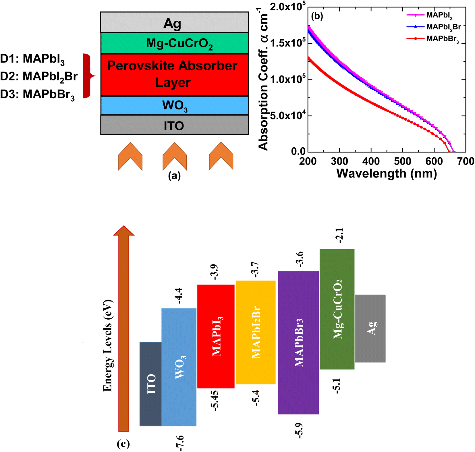 | ||
| Fig. 1 (a) The proposed architecture of MA-based PSC, (b) absorption coefficient of perovskite materials under the illuminance of AM1.5G, and band energy diagram of PSCs. | ||
| Parameters | Terms | ETL (WO3) | PAL1 (MAPbI3) | PAL2 (MAPbBr3) | PAL3 (MAPbI2Br) | HTL (Mg–CuCrO2) |
|---|---|---|---|---|---|---|
| d (μm) | Thicknesses | 0.1–0.15 | 0.2–1.2 | 0.2–1.2 | 0.2–1.2 | 0.1–0.15 |
| Eg (eV) | Bandgap | 3.2 | 1.55 | 2.3 | 1.7 | 3.0 |
| εr | Relative permittivity | 9 | 6.5 | 6.5 | 15 | 9.5 |
| χ (eV) | Electron affinity | 4.4 | 3.9 | 3.6 | 3.7 | 2.1 |
| Nc (cm−3) | Eff. DoS at CB. | 1 × 10²⁰ | 2.2 × 10¹⁸ | 2.2 × 10¹⁸ | 3 × 10¹⁷ | 1 ×10¹⁹ |
| Nv (cm−3) | Eff. DoS at VB. | 2 × 10²¹ | 1.8 × 10¹⁸ | 1.8 × 10¹⁹ | 4 × 10¹⁸ | 1 ×10¹⁹ |
| μn (cm2 V−1 s−1) | Mobility of e | 100 | 2 | 20 | 15 | 0.1 |
| μp (cm2 V−1 s−1) | Mobility of h | 25 | 2 | 20 | 15 | 2.53 |
| Da (cm−3) | Dop. den. of the acceptor | 0 | 5.21 × 10⁹ | 0 | 0 | 6.4 × 10¹⁵ |
| Dd (cm−3) | Dop. den. of donor | 1 × 10²¹ | 5.21 × 10⁹ | 0 | 1 × 10¹⁶ | 0 |
| Nt (cm−3) | Def. density | 1 × 10¹⁴ | 1 × 10¹³ | 1 × 10¹³ | 1 × 10¹³ | 1 × 10¹⁴ |
| Parameters | Mg–CuCrO2/PALs | PALs/WO3 |
|---|---|---|
| Defect types | Neutral | Neutral |
| e cap. cross-section (cm2) | 1 × 10⁻¹⁹ | 1 × 10⁻¹⁹ |
| h cap. cross-section (cm2) | 1 × 10⁻¹⁹ | 1 × 10⁻¹⁹ |
| Energy distributions | Single | Single |
| Ref. for def. energy levels | Above the highest EV | Above the highest EV |
| Energy with respect to ref. (eV) | 0.6 | 0.6 |
| Total density (integrated over all energies) (cm−2) | 1 × 10⁹ | 1 × 10⁹ |
In Fig. 1b, the perovskites, namely MAPbI3, MAPbI2Br, and MAPbBr3, are shown with their respective coefficients over the wavelengths. The absorption coefficients are obtained from the simulating software of SCAPS-1D.49–63 On the other hand, the band energy diagram for all the possible constituent layers in the three designs of the perovskites is also depicted in Fig. 1c, respectively.
3. Results and discussion
The discussion in this part is only focused on the findings and analysis of the current study. The results and discussion segment comprise five smaller portions, numbered 3.1 to 3.5. First, if appropriate, a bandgap analysis is performed, followed by impacts on absorber thickness, temperature, and overall defect density. In this part, the contour analysis for the MA-based solar cell has also been studied simultaneously.The work is simulated at 300 K temperature to check the band alignment of the PSC device and obtain the desired results. The following is a detailed investigation of the current work.
3.1 The influence of PAL-thickness in outputs of the PSC
Thickness tuning of the PSC constituent layer is one of the most promising and successful methods for increasing the effectiveness of the PSC device. The PSC was thickened from 0.2–1.2 μm, and the compatible thicknesses for the optimal efficiency of the simulated device were determined. As shown in Fig. 2a, for MAPbI3, the short-circuit current density (JSC) rises from 16 mA cm−2 and reaches the maximum point at 22 mA cm−2 as the PAL thickness increases from 0.2 μm to 1.2 μm. This is due to the absorption rate's proportional dependence on current density. JSC remains constant, i.e., ∼21 mA cm−2 and 8 mA cm−2 for MAPbI2Br and MAPbBr3 throughout the active layer thickness of 1.2 μm, respectively. Fig. 2b depicts the variation in VOC of all three Perovskite materials and the active layer thickness, which ranges from 0.2 μm to 1.2 μm. The device's VOC is at a steady state with increasing thickness inside the PSC. In terms of numbers, the 1.2 μm thick MAPbBr3-PA has a higher VOC value of 1.52 Volt. The devices in Fig. 2c demonstrate the Fill Factor (FF) property. The Fill factor indicates the squareness of the J–V curve and indicates the resistive losses in the device, and higher FF ensures higher output power and conversion efficiency as both the parameters are proportional to each other. The FF of MAPbI3 decreases from 87.2% to 86.9%, while the PAL thickness increases from 0.2 μm to 1.2 μm. Among the three Perovskite materials used, the material MAPbI2Br shows the maximum value. For MAPbI2Br, the FF appears to remain constant, at around 86.2%, and the FF of MAPbBr3 decreases from 87.89% to 86.89% for the PAL thicknesses varying from 0.2 μm to 1.2 μm, respectively. While Fig. 2d depicts PCE, the most crucial feature of the PSC. The PCE of MAPbI3 remains at approximately 17.62% under the said variation of PAL and the PCE of MAPbBr3 eventually reached 9.85% after steadily rising from 5.2% for the thickness values varying from 0.2 μm to 1.2 μm. The PCE of the material MAPbI2Br rises from 14.8% to 22.05% at the maximum thickness level of the perovskite material. It can be noted from the data in Fig. 2d that the increase in PCE is significant during the initial rise in the thickness of the PAL. This is due to an improvement in photon absorption at higher thicknesses which results in an improvement in JSC and PCE. The same can be validated through JSC. However, further increasing the thickness from 1.0 to 1.2 μm the improvement is not that prominent, and the FF trend showed degradation at higher thicknesses. So eventually a saturated JSC and reduced FF will reduce the PCE if PAL thickness is increased beyond a certain limit. The current work offers a better outcome than the previous work by Dipta et al.64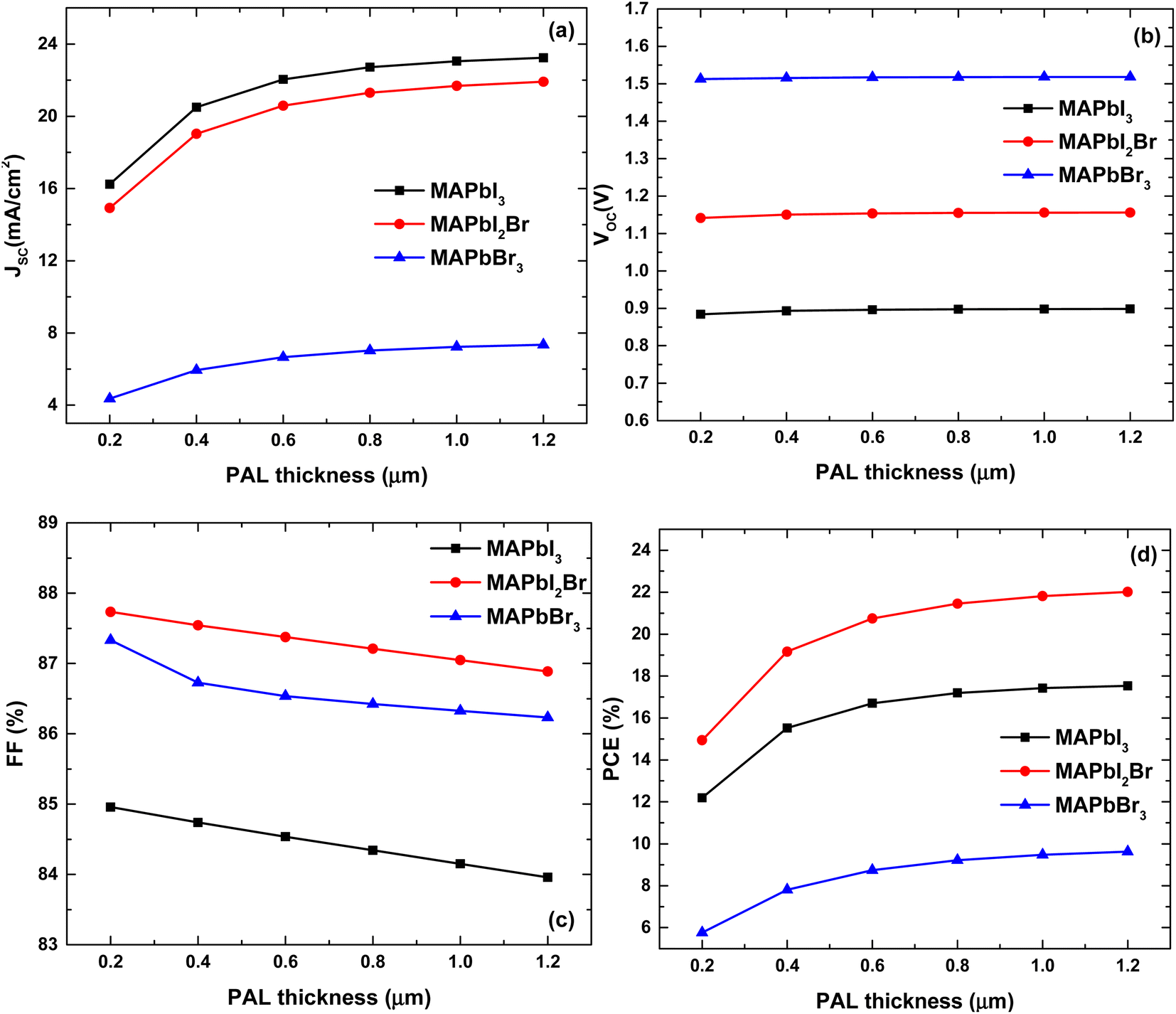 | ||
| Fig. 2 The impact of the perovskite thicknesses on the outputs of the PSC devices. | ||
3.2 The influence of the temperature on the PSC outputs
Fig. 3a and b depicts a comprehensive examination of the PSC properties as temperature changes. As depicted in Fig. 3(a–d), the four parameters JSC, VOC, FF, and PCE decrease as the temperature rises from 300 K–400 K for the Perovskite material MAPbI2Br. The maximum values for the Perovskite MAPbI2Br parameters are 21.91 mA cm−2, 1.16 V, 86.89%, and 22.05% at 300 K.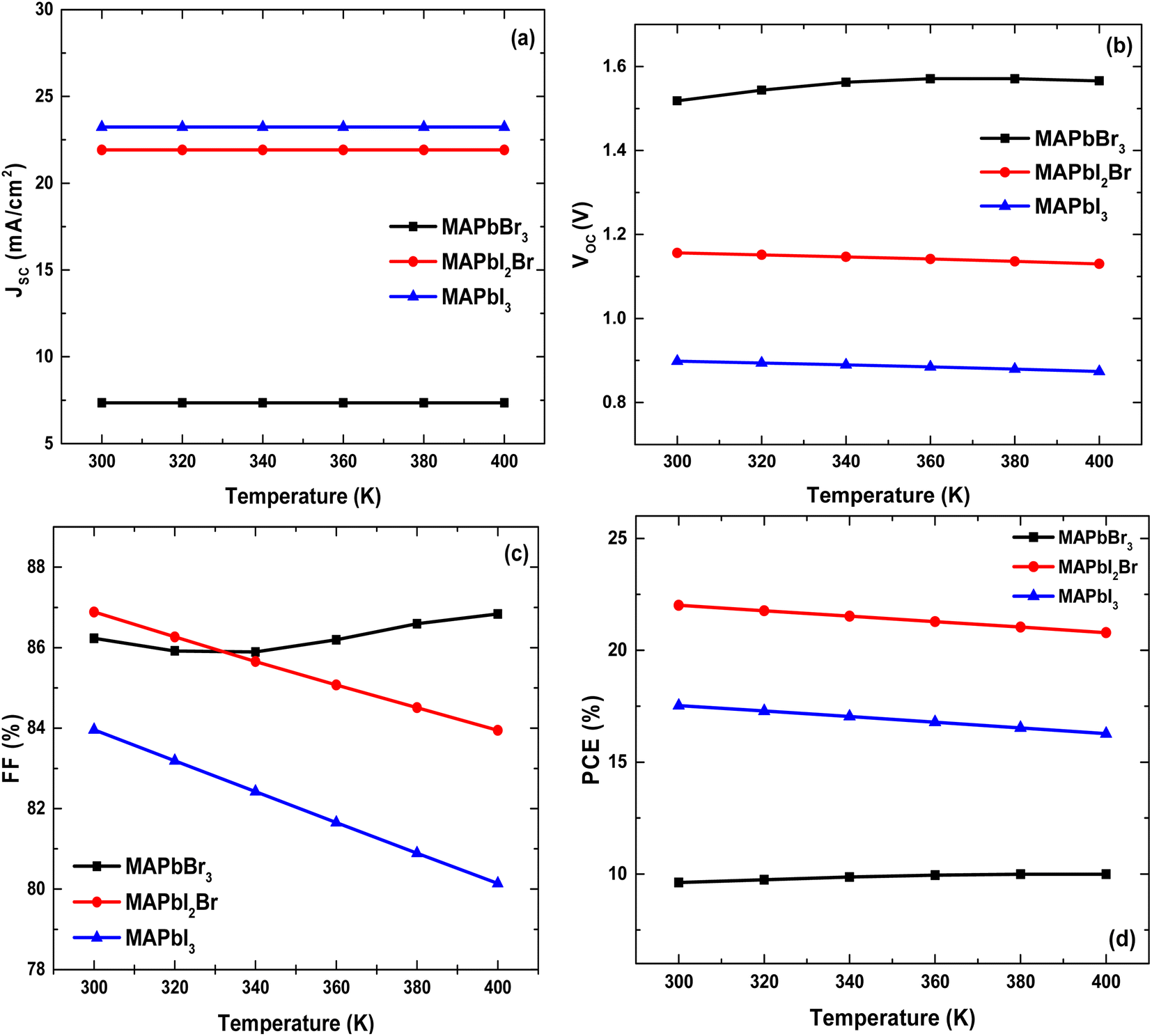 | ||
| Fig. 3 The influence of temperature on the PV parameters of the PSC at the optimized thickness conditions. | ||
For the MAPbBr3, the values of parameters VOC and FF both decrease as the temperature rises from 300 K–400 K, with the maximum values at 300 K being 0.90 V and 81%, respectively. While the value of the parameter JSC rises from 16.6 mA cm−2 to 17.4 mA cm−2 as the temperature increases from 300 K to 400 K, in contrast, PCE remains nearly constant at approximately 9.8% as the temperature increases to the maximum value. Since the increase in temperature reduces the VOC of the PSC devices. As we know, due to the decrease in VOC, the J–V curve becomes steeper, as a result, the FF value is increased as compared to other PSC devices. This is the reason for a nonlinear increase in FF for MAPbBr3-based PSC. And for the material MAPbI3, values of the three parameters JSC, FF, and PCE decrease with increasing temperature from 300 K to 400 K with values of 20.7 mA cm−2, 62%, and 20.8% at peak for the respective parameters at 300 K, but the value of the parameter VOC for the MAPbI3 appears to remain unchanged with a value of 0.982 V while the temperature increases. The current simulation offers an improvement in overall output parameters as compared to the previous work by Bhattarai et al.65
3.3 The combined influence of thickness and total defect density using contour plotting
There are three perovskites devices: firstly, the MAPbI3-based PSC. As Fig. 4 shows the contour plot over the perovskite material's thicknesses and total defect density. The following outcomes can be deduced. Firstly, the PCE is maximum at 1.2 μm thickness and defectivity of 1 × 1013 cm−3, which offers a high value of PCE, i.e., nearly 17.5%. The VOC, on the other hand, is at its maximum, with a value of 1.144 V at 0.2 μm thickness and 1 × 1013 cm−3 defectivity. While the JSC keeps on increasing with the increase in thickness and reduces when the defectivity is higher. The maximum JSC value is 21.03 mA cm−2 at a thickness of 1.2 μm and with a defectivity of 1 × 1018 cm−3. Lastly, the maximum FF is found to be 83% at thickness 0.2 μm thickness and defectivity 1 × 1018 cm−3, respectively.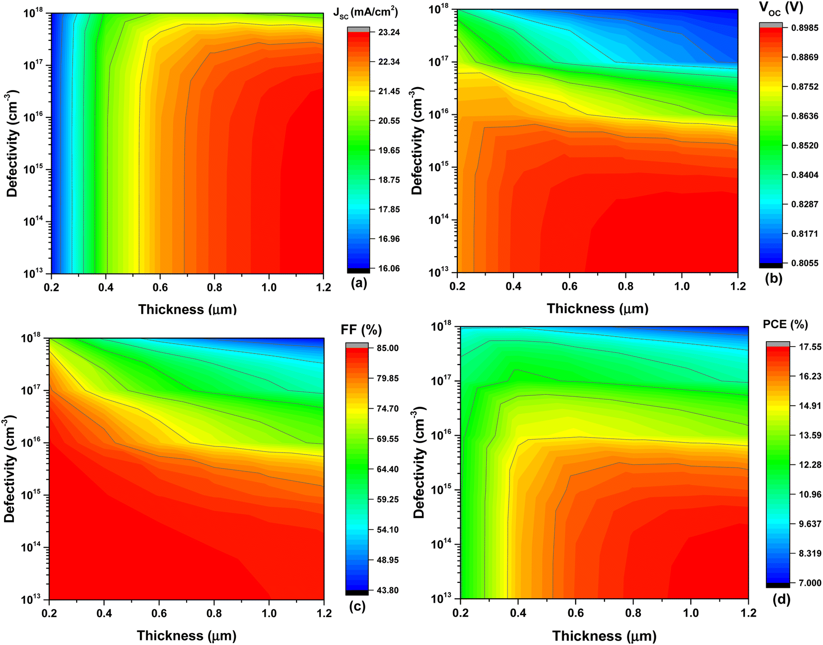 | ||
| Fig. 4 The contour plotting of the perovskite material i.e., MAPbI3 for high output parameters at the optimized temperature and doping conditions. | ||
The second PSC device with the perovskite material of MAPbI2Br offers outstanding device outputs as depicted in Fig. 5. Firstly, the PCE is maximum at 1.2 μm thickness and 1 × 1013 cm−3, which offers a high value of PCE, i.e., nearly a value of 22.05%. On the other hand, the VOC is at maximum with the value of 1.156 V at the higher thickness regions and low defect density region, i.e., 1 × 1013 cm−3 defectivity. At the same time, the JSC keeps on increasing with higher thickness levels and smaller defectivity of the PAL. The maximum JSC value is 21.93 mA cm−2 at a thickness of 1.2 μm and with a defectivity of 1 × 1013 cm−3. Lastly, the maximum FF is found to be 87.80% at a thickness of 1.2 μm and defectivity of 1 × 1018 cm−3, respectively. It can be observed that the four parameters are more predominant for the MAPbI2Br-based PSC as compared to other perovskite materials.
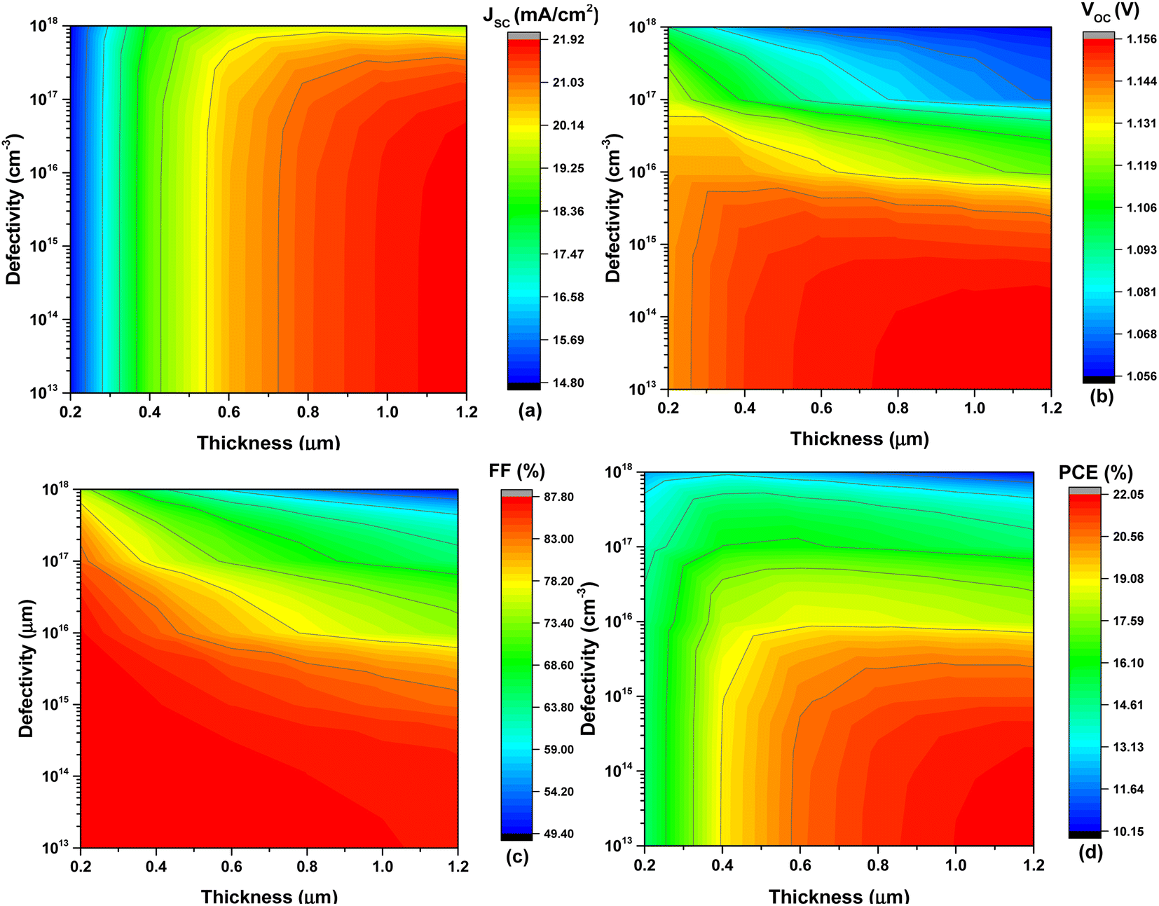 | ||
| Fig. 5 The contour plotting of the perovskite material, i.e., MAPbI2Br, for high output parameters at the optimized temperature and doping conditions. | ||
Fig. 6 depicts how the PCE value continues to increase with the thickness and defectivity for MAPbBr3-based PSC. The maximum value of PCE is 8.935% found at 1.2 μm thickness and 1 × 1013 cm−3 defectivity. While the maximum value of VOC is 1.500 V found at a thickness of 0.2 micrometer and defectivity of 1 × 1013 cm−3, whereas JSC increases with increasing thickness and defectivity, reaching a maximum of 6.971 mA cm−2 at 1.2 μm thickness, and 1 × 1018 cm−3 defectivity. Lastly, the peak value of FF is 82.15%, which is found at 1.2 μm thickness and defectivity 1 × 1018 cm−3. Similar outcomes can be obtained from the previous SCAPS simulated work of Bhattarai et al.66
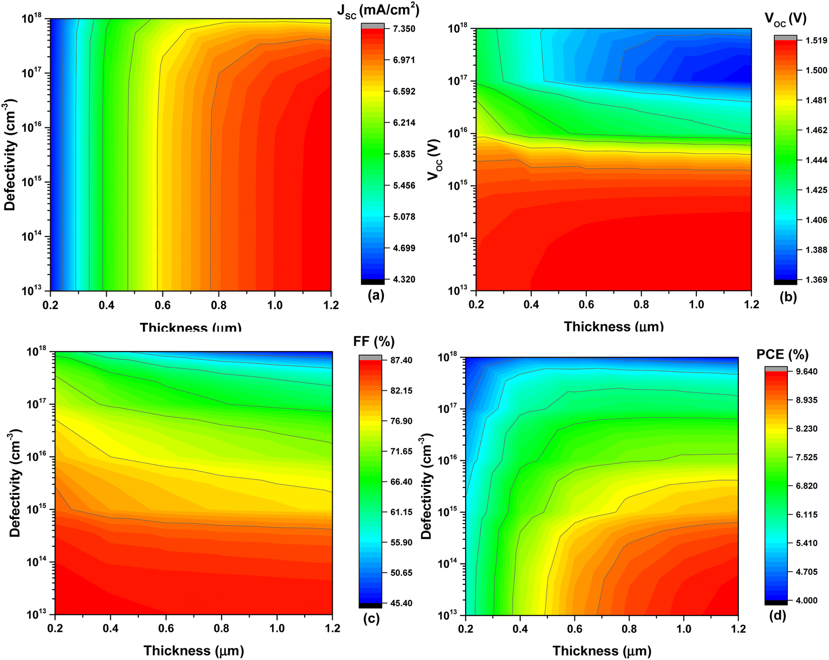 | ||
| Fig. 6 The contour plotting of the perovskite material i.e., MAPbBr3, for high output parameters at the optimized temperature and doping conditions. | ||
3.4 Comparison of impedances of the PSCs
The impedance analysis is one of the better ways to understand the behavior of the perovskite materials having distinct halides. From Fig. 7, it is evident that the highest value of impedance is reached for the MAPbBr3 perovskite, i.e., almost more than 100![[thin space (1/6-em)]](https://www.rsc.org/images/entities/char_2009.gif) 000 ohm cm2. While the Cl2Br-based offers almost nearly 100000 ohm cm2, I-based Perovskite offers 95000 ohm cm2. The previous study also offers a similar impedance value, as depicted in Fig. 8. The report by Bhattarai et al. provides a high value nearly identical to the value obtained in this analysis.67 The impedance plot or Nyquist plot of a solar cell provides a detailed qualitative understanding of resistive losses, capacitance, and recombination rate defects in the device. The impedance curve reported in Fig. 7 shows a similar trend in all three devices with minor changes.
000 ohm cm2. While the Cl2Br-based offers almost nearly 100000 ohm cm2, I-based Perovskite offers 95000 ohm cm2. The previous study also offers a similar impedance value, as depicted in Fig. 8. The report by Bhattarai et al. provides a high value nearly identical to the value obtained in this analysis.67 The impedance plot or Nyquist plot of a solar cell provides a detailed qualitative understanding of resistive losses, capacitance, and recombination rate defects in the device. The impedance curve reported in Fig. 7 shows a similar trend in all three devices with minor changes.
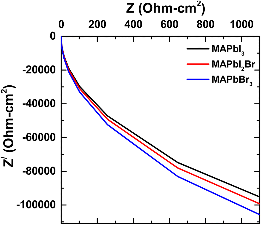 | ||
| Fig. 7 The comparison of impedance (real vs. imaginary) for all three perovskites. | ||
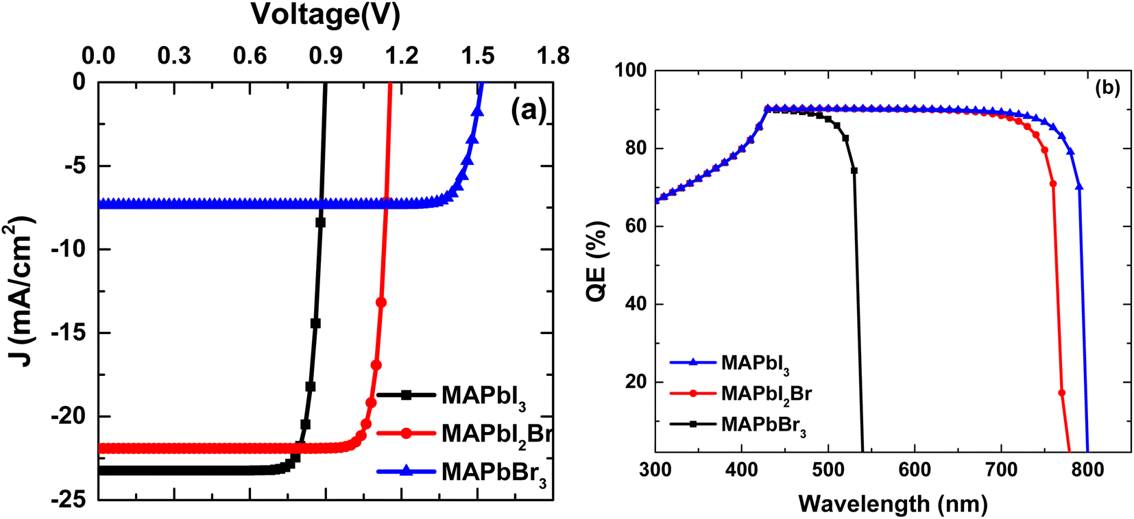 | ||
| Fig. 8 The comparison of J–V and QE of the different perovskite materials. | ||
3.5 Comparison of QE and J–V of the PSCs
The following points are attained from the J–V curve shown in Fig. 8. The MAPbBr3 perovskite attains the highest VOC, nearly 1.5 V, and JSC of 12.5 mA cm−2. Though the VOC is high, the JSC is very low to contribute PCE as the VOC and JSC are directly proportional to the efficiency. On the contrary, the MAPbI3-based PSC offers the smallest value of VOC, which is unsuitable for better efficiency. The MAPbI3 attains the highest VOC of 0.9 V and 23 mA cm−2 value of JSC as shown in Fig. 8a. Since the need of obtaining the best combination of VOC and JSC is mainly necessary. The MAPbI2Br attains the highest VOC of 1.1 V and 22 mA cm−2 of JSC, which offers an excellent efficiency value. The result can be compared with previous work by Adhikari et al.68 The J–V curve of MAPbI2Br also shows that a higher value of FF can be reached, as the steep curve of J–V is higher than the other two materials for better efficiency.As from the QE curve in Fig. 8b, it is found that all three perovskites show high QE values. Comparatively, the highest bandgap perovskite of MAPbBr3 drops at a very small wavelength of nearly 540 nm as the dependency of QE is reciprocal to each other. The lowest bandgap material of MAPbI3 drops at the highest point of wavelength, i.e., nearly 800 nm, as the bandgap is almost 1.5 eV (MAPbI3). The result can be matched with the previous work by Jayan et al.48 The overall comparison of the present work with the previous works is reported in Table 3.
4. Conclusions
The simulation and investigation of the PSC structure with different perovskite materials having a configuration of ITO/WO3/PAL/Mg-CuCrO2/Ag have been utilized using SCAPS-1D simulating software. The WO3 has been used as ETL, keeping in view of maximizing the suitable band alignment and higher mobility of the carrier with the perovskite material in the solar devices, whereas, for the collection of the holes, Mg–CuCrO2 as the HTL for the numerical simulation of the PSC device. Distinctive halide-based methylammonium-based perovskites are used as active PAL that shows a greater influence on the output parameter than the e–h transport layers of the PSC device. So, the optimization of the absorber's thicknesses for the PSC is carried out for better outputs. The work attained an optimal absorber thickness of 1.2 μm for the MAPbI2Br-based PSC device. The defectivity of the PSC shows that at the level of 1 × 1013 cm−3, which obtains higher outputs. Moreover, the study also includes the impact of the resistances for enhancing the higher efficiency of the PSC device. The simulation clearly exhibits that the MAPbI2Br can provide excellent outputs, as in the present case, nearly 22.05%, which may be a fascinating and suitable option in developing the PSC device. The overall conclusion of the present study thus may offer valuable contribution regarding the manufacturing of more efficient MAPbI2Br-based PSC devices. It is also worth to note that the SCAPS-1D simulator used in this work is applicable to one-dimensional devices and cannot support complex device geometry. Therefore, advanced device simulators can also be considered in future work.Data availability
The raw/processed data required to reproduce these findings cannot be shared at this time as the data also forms part of an ongoing study.Conflicts of interest
The authors declare that they have no known competing financial interests or personal relationships that could have appeared to influence the work reported in this paper.Acknowledgements
The authors have extended their appreciation to the Deanship of Scientific Research at King Khalid University, Saudi Arabia for funding this work through Research Groups Program under grant number R.G.P.2: 219/44. The SCAPS-1D program was kindly provided by Dr M. Burgelman of the University of Gent in Belgium. The authors would like to express their gratitude to him.References
- S. Bhattarai, A. Mhamdi, I. Hossain, Y. Raoui, R. Pandey, J. Madan, A. Bouazizi, M. Maiti, D. Gogoi and A. Sharma, Micro Nanostruct., 2022, 172, 207450 CrossRef CAS
.
- S. Karthick, S. Velumani and J. Bouclé, Opt. Mater., 2022, 126, 112250 CrossRef CAS
- F. Azri, A. Meftah, N. Sengouga and A. Meftah, Sol. Energy, 2019, 181, 372–378 CrossRef CAS
- R. Pandey, J. Madan and R. Sharma, IEEE Trans. Electron Devices, 2021, 68, 1757–1763 CAS
- R. Pandey, S. Bhattarai, K. Sharma, J. Madan, A. K. Al-Mousoi, M. K. A. Mohammed and M. K. Hossain, ACS Appl. Electron. Mater., 2023, 5(6), 2431–2460 Search PubMed
- D. Muchahary, S. Bhattarai, A. K. Mahato and S. Maity, in Emerging Materials, Springer Nature Singapore, Singapore, 2022, pp. 361–406 Search PubMed
- C. Devi and R. Mehra, J. Mater. Sci., 2019, 54, 5615–5624 CrossRef CAS
- N. Gamal, S. H. Sedky, A. Shaker and M. Fedawy, Optik, 2021, 242, 167306 CrossRef CAS
- D. Muchahary, L. S. Ram, R. Narzary, P. P. Sahu, S. Bhattarai and S. Tayal, Curr. Appl. Phys., 2022, 38, 15–21 CrossRef
- F. H. Isikgor, S. Zhumagali, L. V. T. Merino, M. De Bastiani, I. McCulloch and S. De Wolf, Nat. Rev. Mater., 2023, 8, 89–108 CrossRef CAS
- A. S. R. Bati, Y. L. Zhong, P. L. Burn, M. K. Nazeeruddin, P. E. Shaw and M. Batmunkh, Commun. Mater., 2023, 4, 2 CrossRef CAS
- Z. Zhang, L. Qiao, K. Meng, R. Long, G. Chen and P. Gao, Chem. Soc. Rev., 2023, 52, 163–195 RSC
- S. Bhattarai and T. D. Das, Opt. Mater., 2021, 111, 110661 CrossRef CAS
- S. Bhattarai and T. D. Das, Sol. Energy, 2021, 217, 200–207 CrossRef CAS
- H. Bencherif, F. Meddour, M. H. Elshorbagy, M. K. Hossain, A. Cuadrado, M. A. Abdi, T. Bendib, S. Kouda and J. Alda, Micro Nanostruct., 2022, 171, 207403 CrossRef CAS
- W. S. Yang, B.-W. W. Park, E. H. Jung, N. J. Jeon, Y. C. Kim, D. U. Lee, S. S. Shin, J. Seo, E. K. Kim, J. H. Noh and S. Il Seok, Science, 2017, 356, 1376–1379 CrossRef CAS PubMed
- K. Fatema and M. S. Arefin, Opt. Mater., 2022, 125, 112036 CrossRef CAS
- P. Srivastava, Sadanand, S. Rai, P. Lohia, D. K. Dwivedi, H. Qasem, A. Umar, S. Akbar, H. Algadi and S. Baskoutas, Phys. Scr., 2022, 97, 125004 CrossRef
- A. Kojima, K. Teshima, Y. Shirai and T. Miyasaka, J. Am. Chem. Soc., 2009, 131, 6050–6051 CrossRef CAS PubMed
- G. Pindolia, S. M. Shinde and P. K. Jha, Mater. Chem. Phys., 2023, 297, 127426 CrossRef CAS
- A. Thakur, D. Singh and S. Kaur Gill, Mater. Today: Proc., 2022, 71, 195–201 CrossRef CAS
- S. Mushtaq, S. Tahir, A. Ashfaq, R. Sebastian Bonilla, M. Haneef, R. Saeed, W. Ahmad and N. Amin, Sol. Energy, 2023, 249, 401–413 CrossRef CAS
- S. Bhattarai, A. Sharma, P. K. Swain and T. D. Das, J. Electron. Mater., 2021, 50, 6756–6765 CrossRef CAS
- S. Bhattarai, A. Sharma, D. Muchahary, M. Gogoi and T. D. Das, Optik, 2021, 243, 167492 CrossRef CAS
- M. K. Hossain, M. K. A. Mohammed, R. Pandey, A. A. Arnab, M. H. K. Rubel, K. M. Hossain, M. H. Ali, M. F. Rahman, H. Bencherif, J. Madan, M. R. Islam, D. P. Samajdar and S. Bhattarai, Energy Fuels, 2023, 37, 6078–6098 CrossRef CAS
- T. Dureja, A. Garg, S. Bhalla, D. Bhutani and A. Khanna, Mater. Today: Proc., 2022, 71, 239–242 CrossRef CAS
- Y. Raoui, H. Ez-Zahraouy, N. Tahiri, O. El Bounagui, S. Ahmad and S. Kazim, Sol. Energy, 2019, 193, 948–955 CrossRef CAS
- A. K. Al-Mousoi, M. K. A. Mohammed, A. Kumar, R. Pandey, J. Madan, D. Dastan, M. K. Hossain, P. Sakthivel, G. Anandha babu and Z. M. Yaseen, Phys. Chem. Chem. Phys., 2023, 25, 16459–16468 RSC
- N. Shrivastav, J. Madan, M. K. A. Mohammed, M. K. Hossain and R. Pandey, Mater. Res. Express, 2023, 10, 075506 CrossRef
- D. Dastan, M. K. A. Mohammed, A. K. Al-Mousoi, A. Kumar, S. Q. Salih, P. S. JosephNg, D. S. Ahmed, R. Pandey, Z. M. Yaseen and M. K. Hossain, Sci. Rep., 2023, 13, 9076 CrossRef CAS PubMed
- R. Pandey, A. Khanna, K. Singh, S. K. Patel, H. Singh and J. Madan, Sol. Energy, 2020, 207, 893–902 CrossRef CAS
- H. Xiao, C. Zuo, K. Yan, Z. Jin, Y. Cheng, H. Tian, Z. Xiao, F. Liu, Y. Ding and L. Ding, Adv. Energy Mater., 2023, 13, 2300738 CrossRef CAS
- S. Bhattarai, M. K. Hossain, R. Pandey, J. Madan, D. P. Samajdar, M. F. Rahman, M. Z. Ansari and M. Amami, Energy Fuels, 2023, 37(14), 10631–10641 CrossRef CAS
- N. Shrivastav, J. Madan, M. K. A. Mohammed, M. K. K. Hossain, R. Pandey, M. K. A. Mohammed, M. K. K. Hossain and R. Pandey, Mater. Res. Express, 2023, 10, 075506 CrossRef
- R. L. Milot, G. E. Eperon, T. Green, H. J. Snaith, M. B. Johnston and L. M. Herz, J. Phys. Chem. Lett., 2016, 7, 4178–4184 CrossRef CAS PubMed
- S. J. Lee, S. S. Shin, Y. C. Kim, D. Kim, T. K. Ahn, J. H. Noh, J. Seo and S. Il Seok, J. Am. Chem. Soc., 2016, 138, 3974–3977 CrossRef CAS PubMed
- H. Ban, T. Nakajima, Z. Liu, H. Yu, Q. Sun, L. Dai, Y. Shen, X.-L. Zhang, J. Zhu, P. Chen and M. Wang, J. Mater. Chem. A, 2022, 10, 3642–3649 RSC
- S. Abdelaziz, A. Zekry, A. Shaker and M. Abouelatta, Opt. Mater., 2020, 101, 109738 CrossRef CAS
- C. Li, X. Wang, E. Bi, F. Jiang, S. M. Park, Y. Li, L. Chen, Z. Wang, L. Zeng, H. Chen, Y. Liu, C. R. Grice, A. Abudulimu, J. Chung, Y. Xian, T. Zhu, H. Lai, B. Chen, R. J. Ellingson, F. Fu, D. S. Ginger, Z. Song, E. H. Sargent and Y. Yan, Science, 2023, 379, 690–694 CrossRef CAS PubMed
- M. K. Hossain, G. F. I. I. Toki, I. Alam, R. Pandey, D. P. Samajdar, M. F. Rahman, M. R. Islam, M. H. K. K. Rubel, H. Bencherif, J. Madan and M. K. A. A. Mohammed, New J. Chem., 2023, 47, 4801–4817 RSC
- N. Shrivastav, S. Kashyap, J. Madan, A. K. Al-Mousoi, M. K. A. Mohammed, M. K. Hossain, R. Pandey and J. Ramanujam, Energy Fuels, 2023, 37, 3083–3090 CrossRef CAS
- S. Bhattarai, R. Pandey, J. Madan, A. Mhamdi, A. Bouazizi, D. Muchahary, D. Gogoi, A. Sharma and T. D. Das, IEEE Trans. Electron Devices, 2022, 69, 3217–3224 CAS
- D. Cao, Z. Li, W. Li, K. Pei, X. Zhang, L. Wan, L. Zhao, A. Cherevan, D. Eder and S. Wang, Mater. Chem. Front., 2023, 7, 964–974 RSC
- S. Brittman and E. C. Garnett, J. Phys. Chem. C, 2016, 120, 616–620 CrossRef CAS
- S. Mehra, R. Pandey, J. Madan, R. Sharma, L. Goswami, G. Gupta, A. K. Srivastava and S. Sharma, SSRN Electron. J., 2022 DOI:10.2139/ssrn.4189425
- R. Singh, M. Parashar, S. Sandhu, K. Yoo and J.-J. Lee, Sol. Energy, 2021, 220, 43–50 CrossRef CAS
- D. K. Sarkar, M. Mottakin, A. K. M. Hasan, V. Selvanathan, S. Khan, M. N. I. Khan, A. F. M. Rabbani, M. Shahinuzzaman, M. Aminuzzaman, F. H. Anuar, T. Suemasu, K. Sopian and M. Akhtaruzzaman, SSRN Electron. J., 2023 DOI:10.2139/ssrn.4236191
- K. D. Jayan and V. Sebastian, Semicond. Sci. Technol., 2021, 36, 065010 CrossRef CAS
- M. Kumar, A. Raj, A. Kumar and A. Anshul, Opt. Mater., 2020, 108, 110213 CrossRef CAS
- G. Pindolia, S. M. Shinde and P. K. Jha, Sol. Energy, 2022, 236, 802–821 CrossRef CAS
- M. K. Hossain, G. F. Ishraque Toki, D. P. Samajdar, M. H. K. Rubel, M. Mushtaq, M. R. Islam, M. F. Rahman, S. Bhattarai, H. Bencherif, M. K. A. Mohammed, R. Pandey and J. Madan, Energy Fuels, 2023, 37, 7380–7400 CrossRef CAS
- K. Chakraborty, M. G. Choudhury and S. Paul, Sol. Energy, 2019, 194, 886–892 CrossRef CAS
- S. Bhattarai, R. Pandey, J. Madan, Z. Ansari, M. K. Hossain, M. Amami, S. H. Ahammad and A. N. Z. Rashed, Prog. Photovoltaics Res. Appl. Res. Appl., 2023 DOI:10.1002/pip.3732
- N. Shrivastav, J. Madan, M. K. A. Mohammed, A. K. Al-Mousoi, M. K. Hossain, M. Amami, M. F. Rahman, D. P. Samajdar, S. Bhattarai and R. Pandey, Mater. Today Commun., 2023, 36, 106761 CrossRef CAS
- S. Bhattarai, D. Jayan, A. Yousfi, M. Chowdhury, M. F. Rahman, R. Pandey, J. Madan, Z. Ansari and M. K. Hossain, Phys. Scr., 2023, 98(9), 095507 CrossRef
- M. K. Hossain, G. F. I. Toki, D. P. Samajdar, M. Mushtaq, M. H. K. Rubel, R. Pandey, J. Madan, M. K. A. Mohammed, M. R. Islam, M. F. Rahman and H. Bencherif, ACS Omega, 2023, 8, 22466–22485 CrossRef CAS PubMed
- S. Ahmed, F. Jannat, M. A. K. Khan and M. A. Alim, Optik, 2021, 225, 165765 CrossRef CAS
- S. Kashyap, J. Madan, M. K. A. Mohammed, M. K. Hossain, S. Ponnusamy and R. Pandey, Mater. Lett., 2023, 339, 134096 CrossRef CAS
- S. Abdelaziz, A. Zekry, A. Shaker and M. Abouelatta, Opt. Mater., 2020, 101, 109738 CrossRef CAS
- S. Karthick, S. Velumani and J. Bouclé, Sol. Energy, 2020, 205, 349–357 CrossRef CAS
- K. Tan, P. Lin, G. Wang, Y. Liu, Z. Xu and Y. Lin, Solid-State Electron., 2016, 126, 75–80 CrossRef CAS
- M. K. Hossain, M. S. Uddin, G. F. I. Toki, M. K. A. Mohammed, R. Pandey, J. Madan, M. F. Rahman, M. R. Islam, S. Bhattarai, H. Bencherif, D. P. Samajdar, M. Amami and D. K. Dwivedi, RSC Adv., 2023, 13, 23514–23537 RSC
- M. K. A. Mohammed, A. K. Al-Mousoi, A. Kumar, M. M. Sabugaa, R. Seemaladinne, R. Pandey, J. Madan, M. K. Hossain, B. S. Goud and A. A. Al-Kahtani, J. Alloys Compd., 2023, 963, 171246 CrossRef CAS
- S. S. Dipta, A. Uddin and G. Conibeer, Heliyon, 2022, 8, e11380 CrossRef CAS PubMed
- S. Bhattarai, R. Pandey, J. Madan, D. Muchahary and D. Gogoi, Sol. Energy, 2022, 244, 255–263 CrossRef CAS
- S. Bhattarai, R. Pandey, J. Madan, F. Ahmed and S. Shabnam, Mater. Today Commun., 2022, 33, 104364 CrossRef CAS
- S. Bhattarai, A. Sharma and T. D. Das, Optik, 2020, 224, 165430 CrossRef CAS
- K. R. Adhikari, S. Gurung, B. K. Bhattarai and B. M. Soucase, Phys. Status Solidi C, 2016, 13, 13–17 CrossRef CAS
| This journal is © The Royal Society of Chemistry 2023 |