
 Open Access Article
 This Open Access Article is licensed under a Creative Commons Attribution-Non Commercial 3.0 Unported Licence
Photovoltaic properties of new solar cell based on ideal cubic NaNbO3 thin films: a combined experimental and density functional theory study
Amira Bougoffa *a,
Ala Eddin Mabroukia,
Abdessalem Trabelsia,
Essebti Dhahria and
Kamel Khirounib
*a,
Ala Eddin Mabroukia,
Abdessalem Trabelsia,
Essebti Dhahria and
Kamel Khirounib
aLaboratory of Applied Physics, Faculty of Sciences of Sfax, University of Sfax, B. P. 1171, Sfax, 3000, Tunisia. E-mail: amirabougoffa@gmail.com; Tel: +21626923772
bLaboratory of Physics of Materials and Nanomaterials Applied for Environment, Faculty of Sciences Gabes, University of Gabes, 6079 Gabes, Tunisia
First published on 13th October 2023
Abstract
We explore the photovoltaic properties of a novel homojunction solar cell based on NNO(p)/NNO(n) perovskite by employing a combination of material synthesis, characterization and density functional theory calculations that are novel ideas compared to those previously reported in the literature. The band structure reveals that NaNbO3 introduces a n-type semiconductor. Moreover, using DFT calculation, we created n-NNO by a simple substitution in the O site by 4.16% fluorine atoms. Experimental and DFT calculation reveals that NNO perovskite exhibits a direct bandgap of ∼1.6 eV, with a slightly larger two other direct bandgaps of ∼2.13 and 3.24 eV. After extracting the necessary parameters, an electrical modelization of an n-NNO/p-NNO solar cell is performed by Maple software revealed that the cell conversion efficiency can reach 17% which presents a first path to identify a new solar cell based only on perovskite material.
1. Introduction
Conventional semiconductor devices are generally fabricated based on Si, Ge, GaAs… However, it has been demonstrated that Perovskite based heterojunction exhibit excellent electric and photovoltaic properties thanks to the large absorption coefficient, long diffusion lengths, and high charge carrier mobility.1–5 Recently, organic–inorganic hybrid perovskites and chalcogenide materials have attract a great attention in photovoltaic applications due to their excellent optical and electronic properties where Pb-based hybrid halide perovskite reached 23% of conversion efficiency presenting the highest one for the perovskite-based solar cells.4,6 Unfortunately, the problem of the toxicity and the non-stability of these materials limit their use as solar cell device. Therefore, research efforts are focused on finding non-toxic, stable and high performance materials. Exploration of oxide perovskite without Pb is one interesting way to address both the stability and toxicity issues simultaneously. Sodium niobate (NaNbO3) is characterized by successive phase transitions, which makes them one of the most important multifunctional materials used in various applications. In fact, I. Aulika et al. have already previously the existence of six phase transitions in the temperature range from 173 K to 913 K.7 This behavior demonstrates where its distinctive physical characteristics, like strong electromechanical activity, come from,8–10 high activity in the water split photocatalytic applications,11–13 electronic applications.14–16 The orthorhombic phase of this material is known as a hole-doped ultraviolet light absorber with a large band gap (3.34 eV).17 On the contrary, S. K. Mishra et al. reported that the cubic phase obtained at 913 K shows a narrow band gap of about 1.8 eV.18 Moreover, M. Tyunina et al. reported the appearance of ferroelectric in NaNbO3 thin films.19 This characteristic can be presented as an indication of good photovoltaic performance.20According to R. Nechache et al., the engineering of the band gap of a simple ferroelectric capacitors giving a efficiency up to 8%.21 Other studies have demonstrated that the addition of a thin ferroelectric layer to the silicon p–n junction enhance the photovoltaic properties.22–25 Additionally, the combination of ferroelectrics with halide perovskites leads to an increase in open circuit voltage in a BiFeO3–CH3NH3PbI3 structure.26,27 However, to our best knowledge, no attempts were made to fabricate solar cell based purely on ferroelectrics perovskite materials.
Accordingly, the aim of this work is to investigate the NaNbO3 named below as (NNO) films prepared by sol–gel method and deposited by spray pyrolysis. The crystalline structure of the deposited films was evaluated by X-ray diffraction (XRD) measured at room temperature. A DFT calculation is performed to investigate the structural, optical and electronic properties of NaNbO3 films. UV-visible spectroscopy is employed to measure the optical absorption and the gap energy of the NNO prepared films. After extracting the necessary parameters, an electrical modelization of an n-NNO/p-NNO homojunction is performed by Maple software to make a first path to identify a new solar cell based only on perovskite material.
2. Experimental
2.1. Sol–gel
To prepare the NNO gel, stoichiometric amounts of NaNO3 and NbCl5 with high purity (Sigma-Aldrich, ≥99%) were dissolved in water/ethanol solution (v/v, 1![[thin space (1/6-em)]](https://www.rsc.org/images/entities/char_2009.gif) :9).28 Citric acid, which was also dissolved in the same solvent, was used as chelating agent in the molar ratio 3:1 with metal ions.29 After dissolving in adequate solvents, all precursors were mixed with ethylene glycol as coordinate agent in the molar ratio 1:2 with citric acid.29 A homogenous transparent solution was then achieved which was then heated at 90 °C to obtain NNO white gel.
:9).28 Citric acid, which was also dissolved in the same solvent, was used as chelating agent in the molar ratio 3:1 with metal ions.29 After dissolving in adequate solvents, all precursors were mixed with ethylene glycol as coordinate agent in the molar ratio 1:2 with citric acid.29 A homogenous transparent solution was then achieved which was then heated at 90 °C to obtain NNO white gel.
2.2. Thin film deposition by spray pyrolysis technique
The gel of NNO is dissolved in distilled water and is pulverized on quartz substrate by spray pyrolysis method. The substrate is placed at a distance of about 20 cm from the nozzle and heated at 340 °C. The flow of the solution is fixed at 2 mL min−1. Nitrogen is used as carrying gas with a flow of 6 L min−1 to pulverize the solution on the substrate during 20 min. After cooling, the obtained film is annealed at 900 °C during 2 hours to induce crystallization.2.3. Measurement tools
The crystalline phase and the purity of the NNO films were examined by X-ray diffraction (XRD) using a θ–2θ diffractometer “Philips X'pert X-Ray, CuKα radiation”. Transmission and absorption spectra were also studied by UV-visible spectroscopy employing a “JASCO V-570 UV/Vis/IR” spectrometer.2.4. Computational details
In this investigation, the DFT calculation an important tool to confirm the optical and electronic behavior of the NNO material and then to extract the physical parameters required for the modelization process. In fact, we used ab initio calculations based on the full-potential linearized-augmented plane-wave (FP-LAPW) method as implemented in WIEN2k30 code based on DFT.31,32 We used a 2 × 2 × 1 supercell containing 4 Na, 4 Nb and 16 O to model NaNbO3 sample. For the exchange-correlation potential, we employed a local density approximation (LDA) built from the Perdew–Wang parameterization. The equilibrium lattice parameters were evaluated using the Murnaghan equation of state.33The energy of separation between the valence and core states is −7.0 Ry. The integrations in the Brillouin zone are performed on a 14 × 14 × 4 grid. The convergence of the self-consistent cycles (SCF) was considered when the energy difference between them was less than 10−6 Ry.
3. Results and discussion
3.1. Crystalline structure
Fig. 1a shows the XRD patterns of the NNO/quartz and quartz substrate measured at room temperature. The phase identification and structural analysis of the prepared films were carried out by means of the Rietveld refinement.34 We can clearly see from Fig. 1b, the presence of NNO pure phase confirming then the good quality of experimental routes of the films deposition. The refinement results, illustrated in Table 1, proved an ideal cubic Pm![[3 with combining macron]](https://www.rsc.org/images/entities/char_0033_0304.gif) m structure with a lattice parameter a = 3.93 Å, displayed in Fig. 1c. As compared with several published work, this result presents an excellent step to the optimization of the room temperature structure of NNO material that presented a large phase diagram with temperature variation.
m structure with a lattice parameter a = 3.93 Å, displayed in Fig. 1c. As compared with several published work, this result presents an excellent step to the optimization of the room temperature structure of NNO material that presented a large phase diagram with temperature variation.
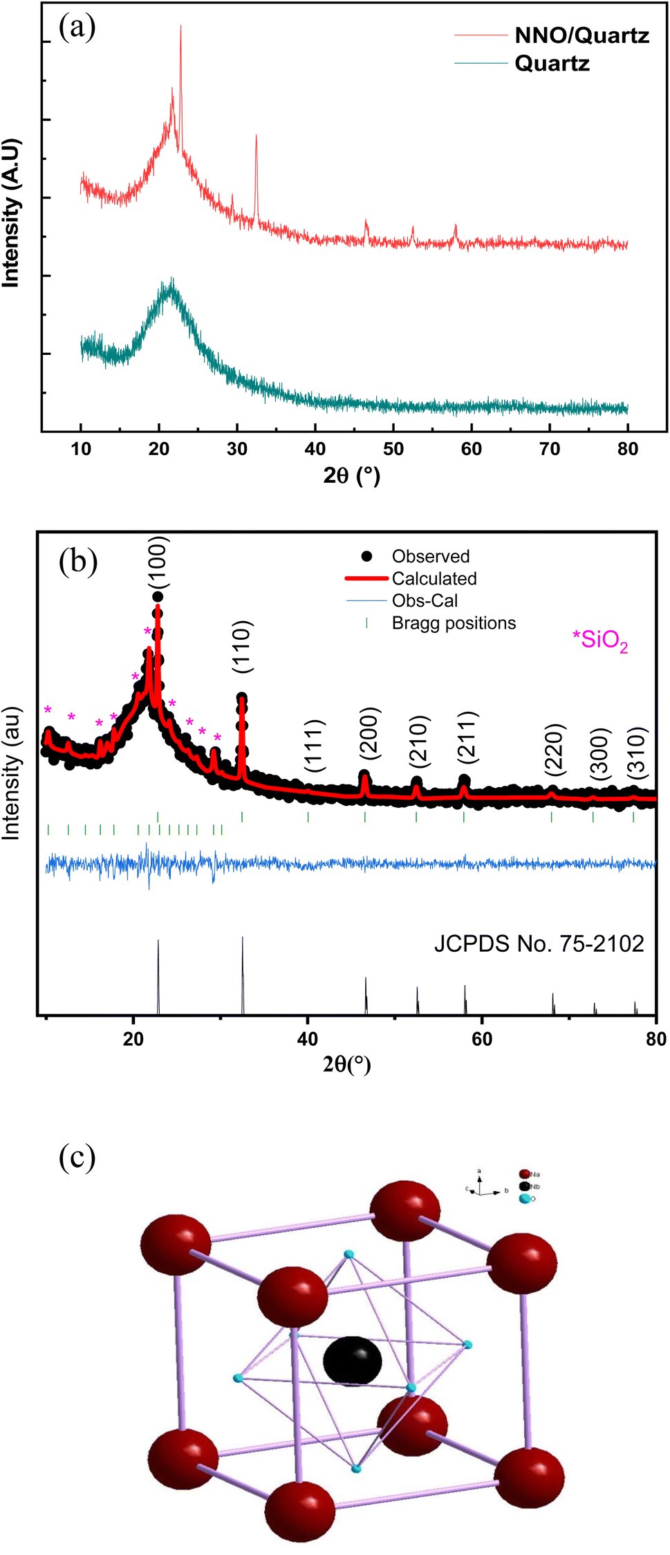 | ||
| Fig. 1 (a) The XRD patterns of the NNO/Quartz and Quartz substrate. (b) The Rietveld refinement the XRD patterns of the NNO and Quartz. (c) Presentation of the ideal cubic structure of NNO material. | ||
| Space group | Pmm |
| Lattice parameter | 3.93 Å |
| Volume | 59.20 Å3 |
| χ2 | 1.109 |
| Na | Nb | O | |
|---|---|---|---|
| x | 0.00 | 0.00 | 0.00 |
| y | 0.50 | 0.50 | 0.50 |
| z | 0.00 | 0.50 | 0.50 |
Additionally, some other diffraction peaks with a low intensity have been detected and were associated to the quartz substrate that may be crystallized during the annealing process at 900 °C according to the X-pert high score software. The refinement of these peaks meaning the FullProof software confirms the m Pnm cubic structure of the SiO2 material.
3.2. DFT calculation
The obtained results revealed a p type semiconducting behavior with a band gap of 1.62 eV as clearly seen from the band structure displayed in Fig. 2a.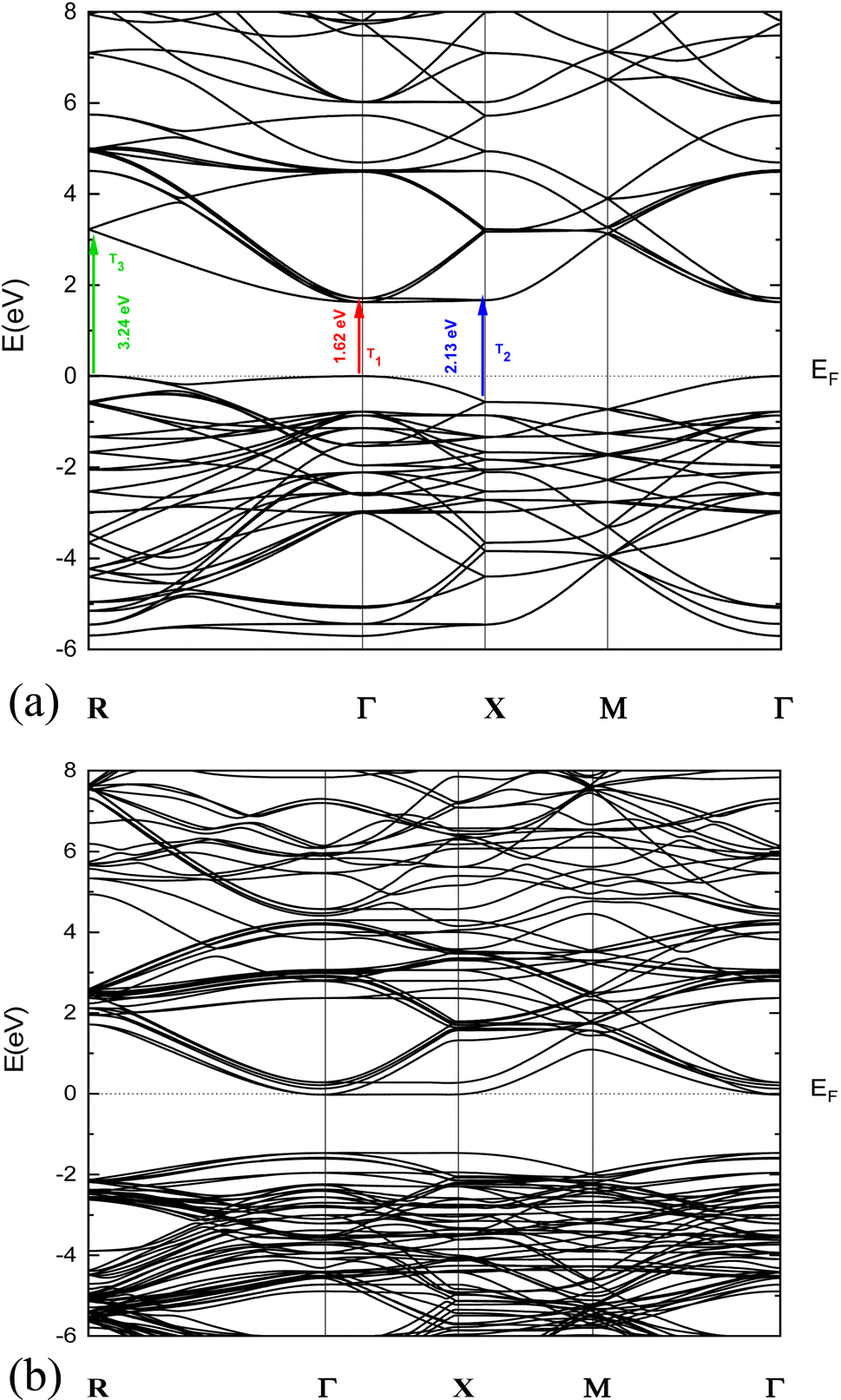 | ||
| Fig. 2 (a) Presentation of the band structure of p-NNO material. (b) Presentation of the band structure of n-NNO material. | ||
In order to obtain an n-type NNO for the modelization of p-NNO/n-NNO solar cell, we have developed a calculation of 4.16% substituted O atom by F one in p-NNO structure based on the investigation of Y. Inaguma et al.35 Therefore, introducing the fluorine atoms in the NNO hosted supercells leads to a change to n-NNO structure with a small variation on the optical properties, as shown in Fig. 2b.
It is important to mention, that the extracted parameters from the DFT calculation present the main key to generate the electrical modelization of NNO based solar cell. Table 2 illustrates the deduced electronic parameters of p-NNO and n-NNO that confirm the semiconducting behavior of these two compounds and their potential candidate to be used in solar cells fabrication.
| p-NNO | n-NNO | |
|---|---|---|
| Eg (eV) | 1.62 | 1.47 |
| Nc (cm−3) | 4.91 × 10¹⁹ | 2.53 × 10¹⁹ |
| Nv (cm−3) | 8.37 × 10¹⁹ | 1.75 × 10²⁰ |
| Ve (m s−1) | 8.84 × 10⁻¹⁵ | 1.10 × 10⁻¹⁴ |
| Vh (m s−1) | 7.40 × 10⁻¹⁵ | 5.78 × 10⁻¹⁵ |
| m* (me) | 1.565 | 1.007 |
| m* (mh) | 2.23 | 3.65 |
| μe (cm2 V−1 s−1) | 3.79 | 494.25 |
| μh (cm2 V−1 s−1) | 168.26 | 0.84 |
| C2De (N m−1) | 26.87 | 32.68 |
| C2Dh (N m−1) | 26.87 | 32.68 |
| |Edα|e (eV) | 6.38 | 0.95 |
| |Edα|h (eV) | 0.95 | 6.38 |
| Ln (μm) | — | 3 |
| Lp (μm) | 3 × 10⁻⁴ | — |
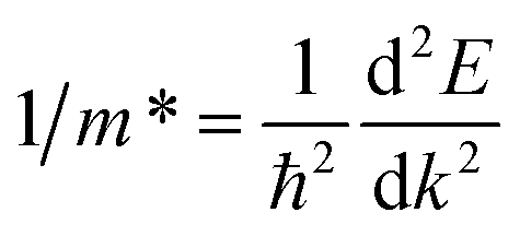
Moreover, referring to the band structure of the two compounds, the effective mass of electron and hole can be deduced by a parabolic fitting of E versus k plots at the bottom of CB and top of VB. They are determined with the expression:36
 | (1) |
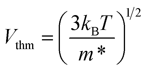
Then, the thermal velocity has been calculated according to the following relation:
 | (2) |
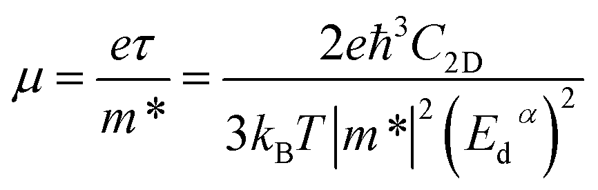
The carrier mobility (μ) can be calculated based on effective mass approximation. The expression of carrier mobility (μ) for 2D material can be written as:37–39
 | (3) |
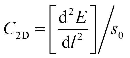 from the plots of Fig. 3a and b, where; E is the total energy of the studied material under external strain, l represents the applied strain and S0 is the area of the optimized supercell.38,39
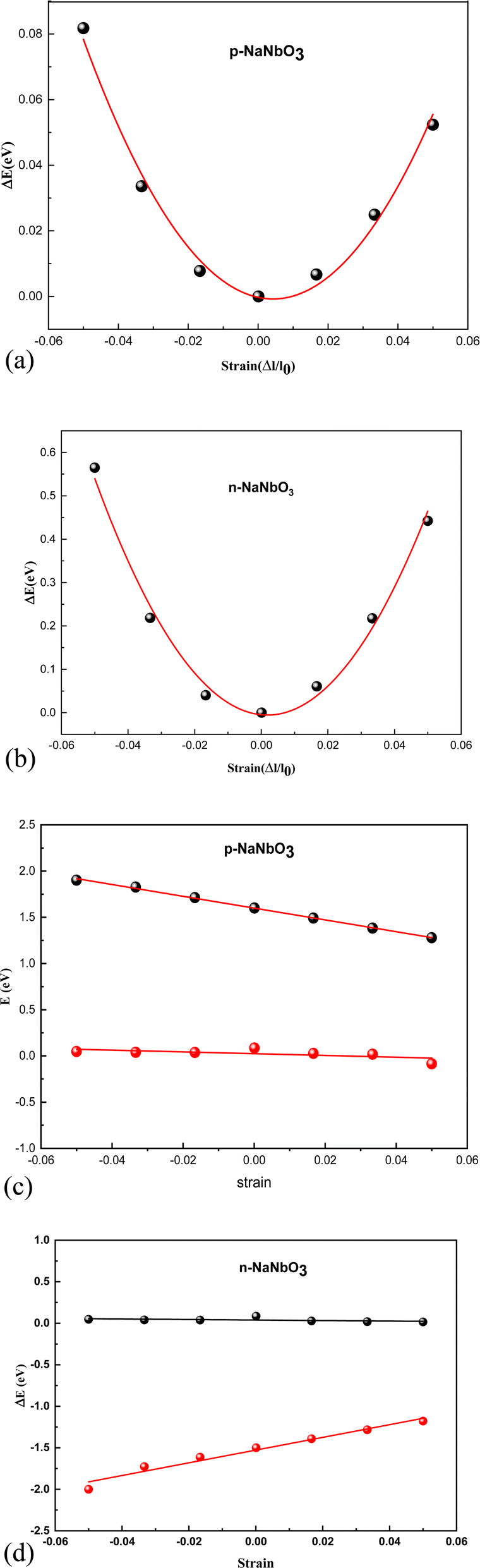 | ||
| Fig. 3 (a) Parabolic fitting of E versus k plots at the top of the valence band. (b) Parabolic fitting of E versus k plots at the bottom of the conduction band. (c) Energy shift of CBM (black symbol) and VBM (red symbol) of p-NaNbO3 with respect to strain. (d) Energy shift of CBM (black symbol) and VBM (red symbol) of n-NaNbO3 with respect to strain. | ||
Edα is the deformation constant which is described by 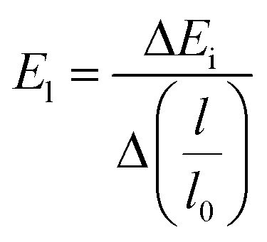 ; where ΔEi is the difference between the CB and VB under external strain obtained from the plots of Fig. 3c and d.
Nc and Nv are defined by:
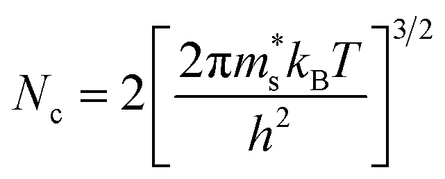 | (4) |
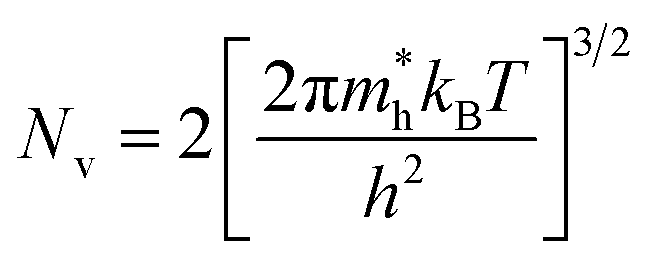 | (5) |
3.3. Optical investigation
Fig. 4a displays the measured UV-visible-IR absorption and transmittance of NNO layer versus the wavelength. We can see that NNO film exhibits an absorption in the visible range accompanied by low transmittance values. In the spectral region where absorption is strongly effective, the absorption coefficient can be analyzed related to the band gap energy. Accordingly, Fig. 4b proves the variation of (αhν)2 versus the incident light energy (hν) according to the following Tauc expression:40| (αhν)2 = A(hν − Eg) | (6) |
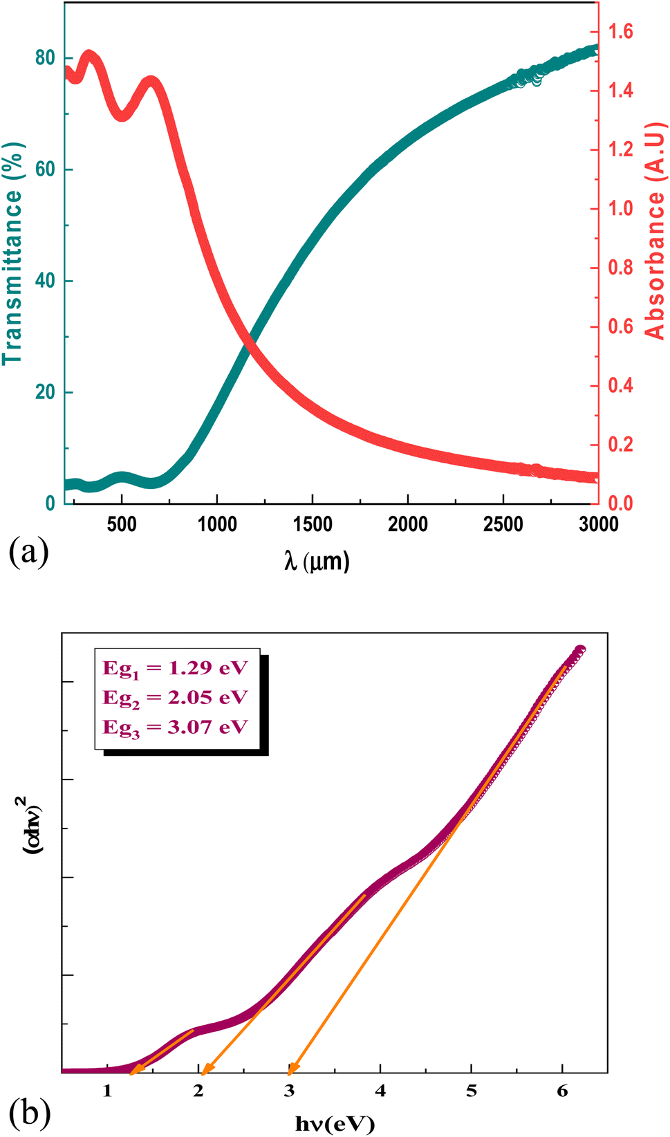 | ||
| Fig. 4 (a) The experimental variation of the transmittance and absorbance of the NNO film versus the wavelength. (b) The plots of (αhν)2 versus (hν) plots of NNO film. | ||
A is a constant and hν is the photon energy.
The gap energy Eg of NNO material was determined according to the previous relation. It is clear three band gap are observed in this figure at 1.29 eV, 2.05 eV and 3.07 eV.
These three optical transitions shown experimentally are also clearly observed in the calculated band structure (Fig. 2a). This shows the presence of three optical transitions along the Γ–Γ, X–X and R–R directions at 1.62, 2.13 and 3.24 eV, respectively. A similar behavior was observed by Maier et al.,41 and Peng et al.42 The origin of this behavior is related to the existence of Multiple Electron Pockets in the Conduction and Valance Bands.41
Fig. 5a displays the theoretical absorption coefficient of p-NNO and n-NNO obtained from the DFT calculation. It is clear that the two materials exhibited more intensive absorption in the UV-visible range that decreases strongly at the high wavelengths regions with a small variation between p-NNO and n-NNO plots with a shifting to the high wavelengths for the n-NNO absorption. This behavior is also confirmed by the variation of the theoretical extinction coefficient shown in Fig. 5b.
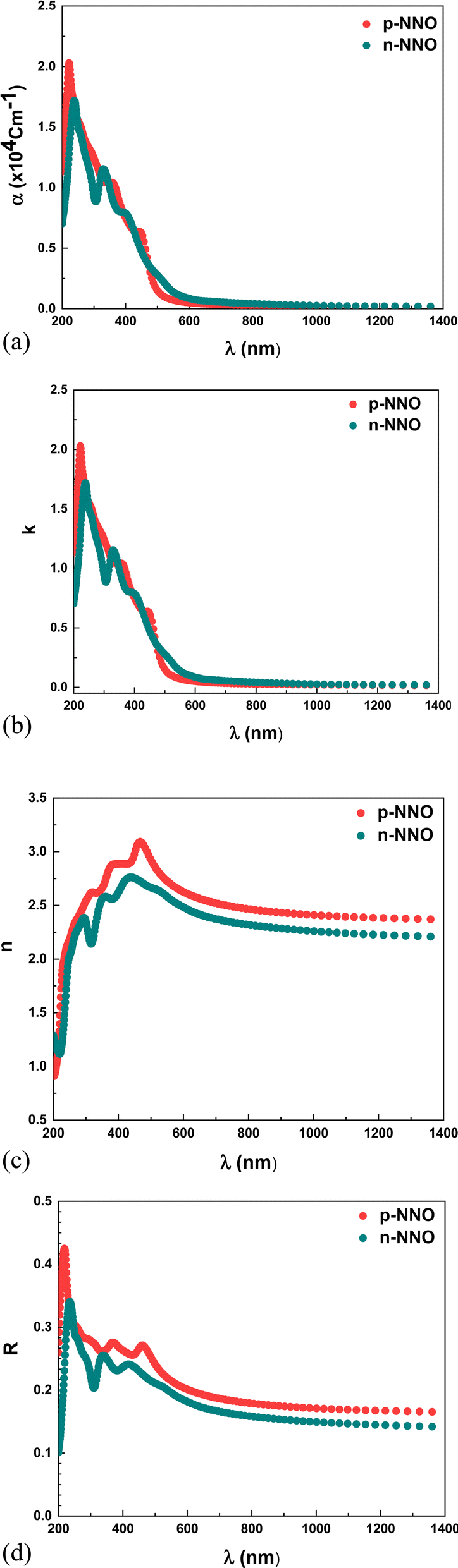 | ||
| Fig. 5 (a) The theoretical variation of the absorption coefficient α extracted from the DFT calculation. (b) The theoretical variation of the extinction coefficient k extracted from the DFT calculation. (c) The theoretical variation of the refractive index n extracted from the DFT calculation. (d) The theoretical variation of the refractive Reflectance extracted from the DFT calculation. | ||
In another hand, the refractive index is an important parameter of materials for technological applications in optical based devices, due to its direct relationship with the dispersion energy. Fig. 5c, shows the theoretical variation of refractive index n extracted from the DFT calculation. As observed, the index n reaches a maximum at the wavelength around 500 nm laying in the absorption region, while it tends to be constant at higher wavelengths (n ≈ 2.5) where it becomes non dispersive. We can assume that the refractive index proves an anomalous dispersion at the lower wavelengths and a normal dispersion at the higher ones.43 Thus the obtained values are close to the experimental data reported by M. Tyunina et al. for epitaxial ferroelectric cubic NNO films.19
As we know, the reflected light at the front surface of the solar cell presents an important factor for that can affect its conversion efficiency. For this reason, the reflectance presents a key parameter for the solar cell structures where minimizing the frontal reflectance is proved to be a main objective requiring the development of specific technologies whose texturing remains the most efficient.44,45 Fig. 5d, shows the variation of the reflectance R of p-NNO and n-NNO versus wavelength obtained from the DFT calculation. As clearly seen, the reflectance plots show the same variation of the refractive index where they remain constant in the region up to 600 nm with a low value about 20% when considering the absence of an anti-reflection layer in the solar cell modelization.
Fig. 6 displays the optical conductivity dependence on wavelength. The high observed optical conductivity, at lower wavelengths (400–600 nm), is attributed to the high light absorption of p-NNO and n-NNO materials. Indeed, the optical conductivity is related to the free charges that absorb the photon energy; a significant rise of the optical conductivity is then expected. Generally, the electrical conductivity is much lower than the optical one by the fact that the free carriers do not acquire necessary energy to jump the potential barrier level46 which can explain the low carriers mobilities values deduced from the DFT calculation.
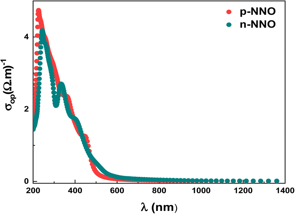 | ||
| Fig. 6 The theoretical variation of the optical conductivity extracted from the DFT calculation. | ||
3.4. Photovoltaic application: electrical modelization of n-NNO/p-NNO solar cell properties
Fig. 7 displays a two-dimensional schematic model for an n-NNO/p-NNO solar cell where n-NNO and p-NNO present the emitter and the base presents regions, respectively.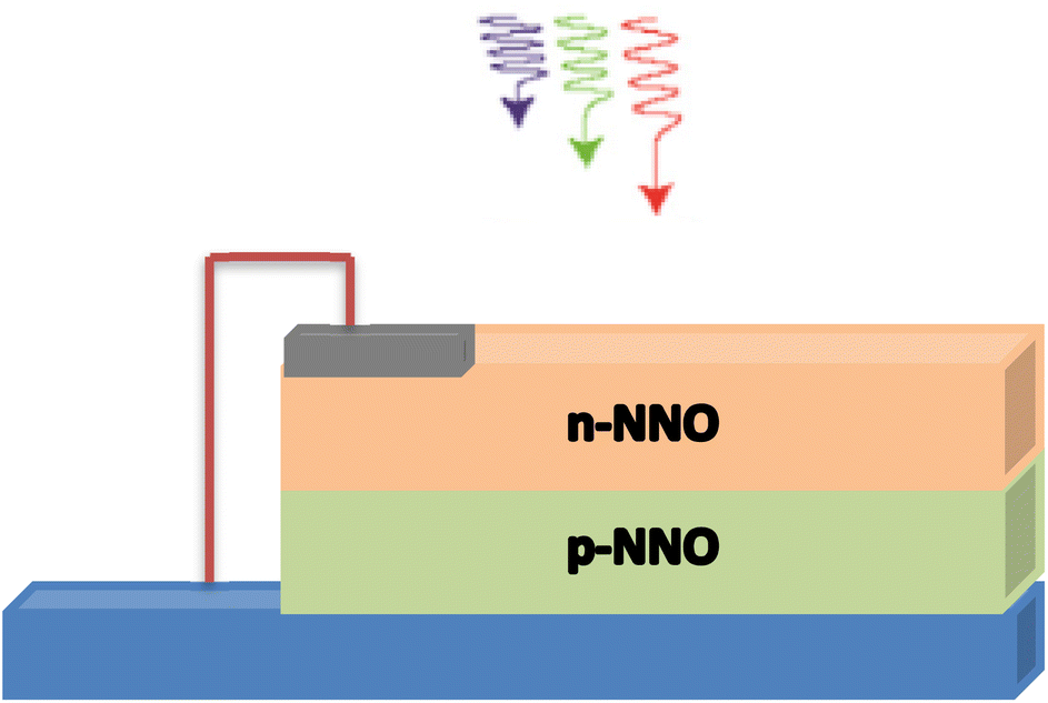 | ||
| Fig. 7 Two-dimensional schematic model for an n-NNO/p-NNO solar cell. | ||
The external quantum efficiency of the cell EQE(λ) presents an important parameter to evaluate the spectral efficiency of the studied cell. It is given by the ratio between the number of electron–hole pairs collected by the junction and the number of photons crossing the surface of the semiconductor per unit time and area, as given by the following expression:
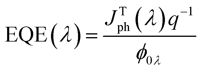 | (7) |
Fig. 8 proves the variation of the total external quantum efficiency (EQETotal) generated by the n-NNO/p-NNO solar cell as well as the contributions of the different cell regions. The results clearly demonstrate that the NNO based cell exhibits a high EQETotal especially in the medium wavelengths. This enhancement is attributed to two reasons. First, it results from the high absorption of NNO material in this region leading to a higher carriers generation.
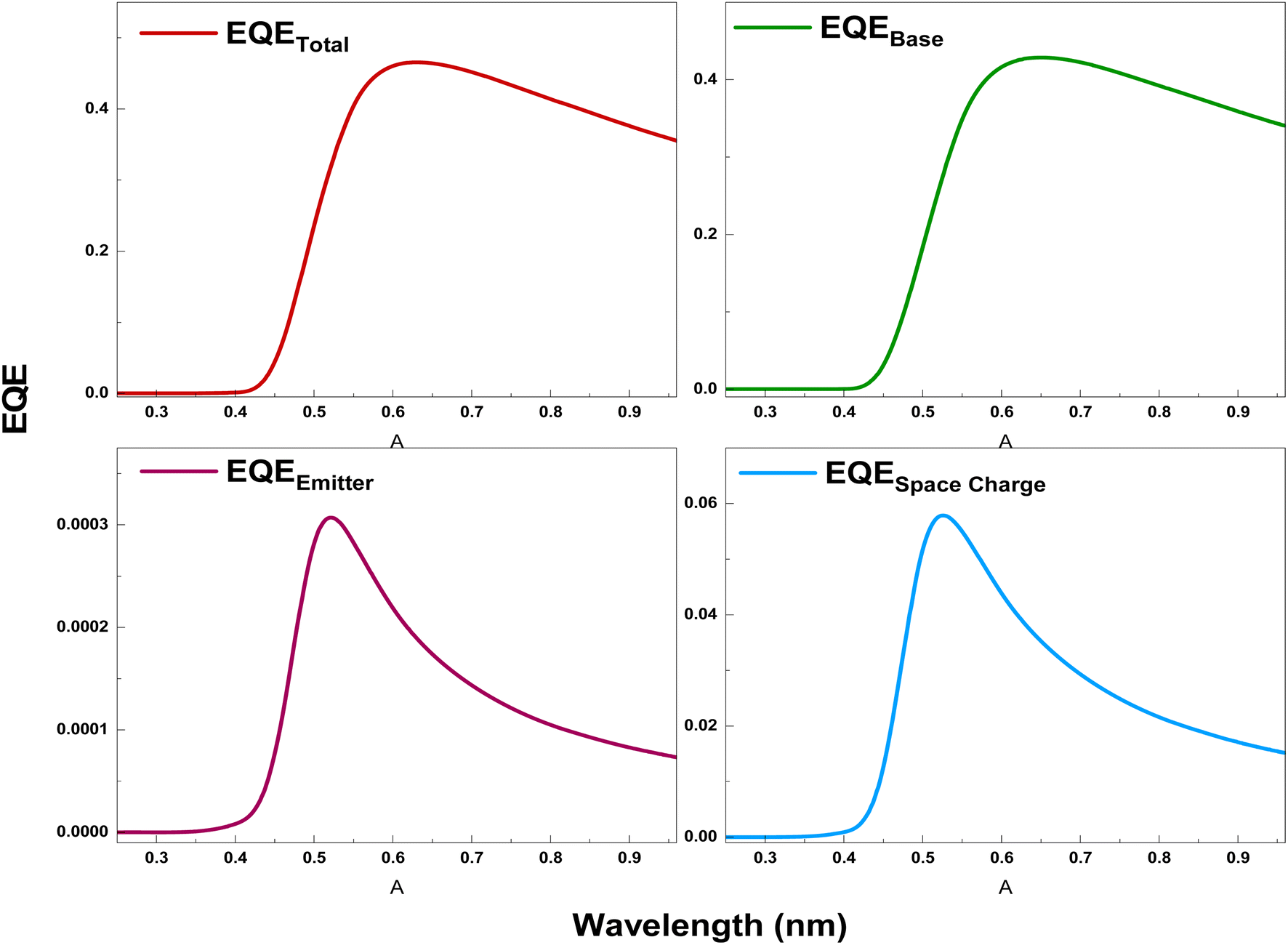 | ||
| Fig. 8 The variation of the EQETotal of the n-NNO/p-NNO solar cell and the contributions of it's different regions. | ||
Second, the low value of the dark current can also reduce the total photocurrent generated by the studied cell. In fact, as demonstrated by the DFT calculation, NNO presents low values of carriers mobility leading two a low diffusion length where carriers will did before contributing to the dark carriers transport which presents an important factor that can affect the total generated current. It is also important to mention, that this investigation have not considered the passivation on the front and back solar cell sides. Further, by considering the experimental results of the NNO film transmittance, we can expect that a high lite portion was lost, especially at the high wavelengths. Therefore, we can assume that the decrease of the EQETotal with the increase of wavelength is attributed to the light loss in this region.45
When observing the contribution of different regions of the EQE, proved also by Fig. 8, we clearly remark that the contribution of the base region is more important than the emitter and the space charges region ones which can be attributed to the fact that electrons present a higher mobility than the holes one. Accordingly, the total cell photocurrent is mainly resulting from the contribution of the base region.
Fig. 9 shows the variation of the cell conversion efficiency η versus the emitter thickness We at two different base thicknesses WB. The obtained results clearly prove that the cell efficiency decrease when the emitter thickness increases, this can be attributed to the significant decrease in the contribution of the base region compared to the increase in the contribution of the emitter one. In the same figure, we have displayed the variation of the short circuit current Jsc and the open-circuit voltage Voc of the NaNbO3 based solar cell versus the emitter thickness. It is clearly seen that these two parameters present the same variation as the cell efficiency with the increase of the emitter thickness which indicate that the variation of the open circuit voltage and the conversion efficiency is mainly attributed to the variation of the photogenerated cell current and then to the absorption coefficient of the NNO material.
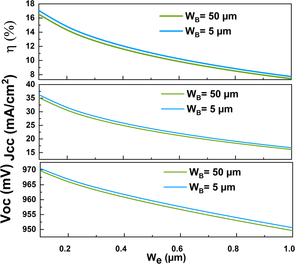 | ||
| Fig. 9 The variation of the conversion efficiency η, the short circuit current density Jsc and the open circuit voltage Voc of the n-NNO/p-NNO cell under the emitter thickness variation. | ||
Thanks to the advances technologies of thin film deposition and as reported by M. Tyunina et al.,19 we can obtain NNO films with thickness about 10 nm. Therefore, it is possible to prepare NNO base solar cell with conversion efficiency close to 17%.
Compared to the conventional solar cells, as a new material for energy conversion, NNO exhibited an excellent efficiency that can be further enhanced by several methods such as, the improvement of the absorption coefficient, the front and back passivation, interface passivation and the front and back contact optimization.47–50 In fact, the charge recombination can be reduced by the interface passivation by oxide deposited layer covered with other dielectric material layer47,51 where SiO2 is used as an interlayer to reduce recombination losses at the front metal-silicon contact of solar cells.52,53 Thus, the agreement between the experimental and theoretical data of the structural and optical properties presents a successful prediction of the photovoltaic behavior that motivates to continue the experimental process and fabricate a first NNO based solar cell.
4. Conclusion
To sum up, in this study, we prepared NNO material prepared by sol–gel method, and then we deposited the obtained material on quartz substrate by spray pyrolysis. The XRD measurement exhibited an ideal Pm3m cubic structure with a lattice parameter a = 3.93 Å. The optical investigation revealed an absorption in the visible range with a direct band gap about 1.29 eV. The DFT calculation proved a p-type semiconducting behavior for the prepared films and a good agreement with the experimental data with a direct band gap about 1.62 eV. After that, the creation of n-NNO structure by means the DFT calculation was created by a substitution of 4.16% of O atoms by fluorine ones. Finally, the electrical modelization of an n-NNO/p-NNO homojunction solar cell was performed by Maple software can achieve a conversion efficiency about 17%.Data availability
All data generated or analyzed during this study are included in this article. Furthermore, the datasets generated during and/or analyzed during the current study are available from the corresponding author on reasonable request.Conflicts of interest
On behalf of all authors, the corresponding author states that there is no conflict of interest.Acknowledgements
The authors would also like to acknowledge the Ministry of Higher Education and Scientific Research of Tunisia for the support this research work within the postdoctoral position.References
- H.-H. Fang, R. Raissa, M. Abdu-Aguye, S. Adjokatse, G. R. Blake, J. Even and M. A. Loi, Photophysics of Organic–Inorganic Hybrid Lead Iodide Perovskite Single Crystals, Adv. Funct. Mater., 2015, 25, 2378 CrossRef CAS
.
- T. C. Sum and N. Mathews, Advancements in perovskite solar cells: photophysics behind the photovoltaics, Energy Environ. Sci., 2014, 7, 2518 RSC
- X. Wu, M. T. Trinh, D. Niesner, H. Zhu, Z. Norman, J. S. Owen, O. Yaffe, B. J. Kudish and X.-Y. Zhu, J. Am. Chem. Soc., 2015, 137, 2089 CrossRef CAS PubMed
- F. Igbari, Z.-K. Wang and L.-S. Liao, Progress of Lead-Free Halide Double Perovskites, Adv. Energy Mater., 2019, 9, 12 Search PubMed
- Y. Sun, J. Zhang and H. Yu, Room-temperature electrochemically deposited polycrystalline SnO2 with adjustable work function for high-efficiency perovskite solar cells, J. Mater. Chem. A, 2023, 11, 901 RSC
- J. Zhang, B. Yu, Y. Sun and H. Yu, Minimized Energy Loss at the Buried Interface of p–i–n Perovskite Solar Cells via Accelerating Charge Transfer and Forming p–n Homojunction, Adv. Energy Mater., 2023, 13, 2300382 CrossRef CAS
- I. Aulika, A. Deyneka, V. Zauls and K. Kundzins, Thermo-optical studies of NaNbO3 thin films, J. Phys.: Conf. Ser., 2007, 93, 012016 CrossRef
- L. A. Reznichenko, N. V. Dergunova, G. A. Geguzina, O. N. Razumovskaya, L. A. Shilkina and L. S. Ivanova, NaNbO3-Based Binary Solid Solutions, Inorg. Mater., 1997, 33, 1277–1284 CAS
- Y. Saito, H. Takao, T. Tani, T. Nonoyama, K. Takatori, T. Homma, T. Nagoya and M. Nakamura, Lead-Free Piezoceramics, Nature, 2004, 432, 84 CrossRef CAS PubMed
- V. Bobnar, B. Malic, J. Holc, M. Kosec, R. Steinhausen and H. Beige, Electrostrictive Effect in Lead-Free Relaxor K0.5Na0.5NbO3–SrTiO3 Ceramic System, J. Appl. Phys., 2005, 98, 024113 CrossRef
- G. Li, T. Kako, D. Wang, Z. Zou and J. Ye, Synthesis and enhanced photocatalytic activity of NaNbO3 prepared by hydrothermal and polymerized complex methods, J. Phys. Chem. Solids, 2008, 69, 2487–2491 CrossRef CAS
- G. Q. Li, Photocatalytic properties of NaNbO3 and Na0.6Ag0.4NbO3 synthesized by polymerized complex method, Mater. Chem. Phys., 2010, 121, 42–46 CrossRef CAS
- S. F. Chen, Y. F. Hu, L. Ji, X. L. Jiang and X. L. Fu, Preparation and characterization of direct Z-scheme photocatalyst Bi2O3/NaNbO3 and its reaction mechanism, Appl. Surf. Sci., 2014, 292, 357–366 CrossRef CAS
- B. Zielińska, E. Borowiak-Palen and R. J. Kalenczuk, Preparation, characterization and photocatalytic activity of metal-loaded NaNbO3, J. Phys. Chem. Solids, 2011, 72, 117–123 CrossRef
- V. Shanker, S. L. Samal, G. K. Pradhan, C. Narayana and A. K. Ganguli, Nanocrystalline NaNbO3 and NaTaO3: Rietveld studies, Raman spectroscopy and dielectric properties, Solid State Sci., 2009, 11, 562–569 CrossRef CAS
- S. Bai, Y. Lu and T. Karaki, Preparation of plate-like sodium niobate particles by hydrothermal method, J. Am. Ceram. Soc., 2015, 98, 654–658 CrossRef CAS
- B. Zielińska, E. Borowiak-Palen and R. J. Kalenczuk, Preparation, characterization and photocatalytic activity of metal-loaded NaNbO3, J. Phys. Chem. Solids, 2011, 72, 117–123 CrossRef
- S. K. Mishra, N. Choudhury, S. L. Chaplot, P. S. R. Krishna and R. Mittal, Competing antiferroelectric and ferroelectric interactions
in NaNbO3: Neutron diffraction and theoretical studies, Phys. Rev. B: Condens. Matter Mater. Phys., 2007, 76, 024110 CrossRef
- M. Tyunina, D. Chvostova, O. Pacherova, T. Kocourek, M. Jelinek, L. Jastrabik and A. Dejneka, Ambience-sensitive optical refraction in ferroelectric nanofilms of NaNbO3, Sci. Technol. Adv. Mater., 2014, 15, 04500 CrossRef PubMed
- Y. Yuan, Z. Xiao, B. Yang and J. Huang, Arising applications of ferroelectric materials in photovoltaic devices, J. Mater. Chem. A, 2014, 2, 6027–6041 RSC
- R. Nechache, C. Harnagea, S. Li, L. Cardenas, W. Huang, J. Chakrabartty and F. Rosei, Bandgap tuning of multiferroic oxide solar cells, Nat. Photonics, 2015, 9, 61–67 CrossRef CAS
- W. Wang, F. Liu, C. M. Lau, L. Wang, G. Yang, D. Zheng and Z. Li, Field-effect BaTiO3-Si solar cells, Appl. Phys. Lett., 2014, 104, 123901 CrossRef
- X. Li, X. Wang, L. Peng, K. Zhang, W. Wu and Y. Tang, Ferroelectric thin film on a silicon based pn junction: Coupling photovoltaic properties, Ferroelectrics, 2016, 500, 250–258 CrossRef CAS
- L. Zhen, T. Rong-Sheng, W. Xiao-Feng and Z. Fen-Gang, An Enhanced Photoelectric Conversion Efficiency of n-Type Crystalline Silicon p–n Junctions Using a Ferroelectric Passivation Layer, Chin. Phys. Lett., 2014, 31, 047701 CrossRef
- Q. Liu, I. Khatri, R. Ishikawa, A. Fujimori, K. Ueno, K. Manabe, H. Nishino and H. Shirai, Improved photovoltaic performance of crystalline-Si/organic Schottky junction solar cells using ferroelectric polymers, Appl. Phys. Lett., 2013, 103, 163503 CrossRef
- P. Zhao, L. Bian, L. Wang, J. Xu and A. Chang, Enhanced open voltage of BiFeO3 polycrystalline film by surface modification of organolead halide perovskite, Appl. Phys. Lett., 2014, 105, 013901 CrossRef
- C. Sun, Y. Guo, B. Fang, J. Yang, B. Qin, H. Duan, Y. Chen, H. Li and H. Liu, Enhanced Photovoltaic Performance of Perovskite Solar Cells Using Polymer P(VDF-TrFE) as a Processed Additive, J. Phys. Chem. C, 2016, 120, 12980–12988 CrossRef CAS
- S. M. Liua, X. B. Zhua, J. Yanga, B. C. Zhao, Z. G. Shenga, W. H. Songa, J. M. Daia and Y. P. Sun, Fabrication of polycrystalline La0.7Sr0.3MnO3 thin films on Si (100) substrates by chemical solution deposition, Phys. Rev. B: Condens. Matter Mater. Phys., 2004, 353, 238–241 CrossRef
- Y. Lina, H. Yang and F. Wang, Preparation and Morphological Controlling of Nanophase NaNbO3 by Sol–Gel Method, Key Eng. Mater., 2008, 368–372, 140–143 Search PubMed
- P. Blaha, K. Schwarz, F. Tran, R. Laskowski, G. K. H. Madsen and L. D. Marks, WIEN2k: An APW+lo program for calculating the properties of solids, J. Chem. Phys., 2020, 152, 074101 CrossRef CAS PubMed
- A. Mabrouki, T. Mnasri, A. Bougoffa, A. Benali, E. Dhahri and M. A. Valente, Experimental study and DFT calculation of the oxygen deficiency effects on structural, magnetic and optical properties of La0.8□0.2MnO3−δ (δ = 0, 0.1 and 0.2) compounds, J. Alloys Compd., 2021, 860, 157922 CrossRef CAS
- A. Mabrouki, O. Messaoudi, M. Mansouri, S. Elgharbi and A. Bardaoui, Study of the structural, electronic, magnetic and magnetocaloric properties of La0.5Ca0.5Mn0.9V0.1O3 sample: first-principles calculation (DFT–MFT), RSC Adv., 2021, 11, 37896–37903 RSC
- F. D. Murnaghan, The Compressibility of Media under Extreme Pressures, Proc. Natl. Acad. Sci. U. S. A., 1944, 30, 244–247 CrossRef CAS PubMed
- H. M. Rietveld, A profile refinement method for nuclear and magnetic structures, J. Appl. Crystallogr., 1965, 2, 65–71 CrossRef
- Y. Inaguma, J.-M. Greneche, M.-P. Crosnier-Lopez, T. Katsumata, Y. Calage and J.-L. Fourque, Structure and Mössbauer Studies of F–O Ordering in Antiferromagnetic Perovskite PbFeO2F, Chem. Mater., 2005, 17, 1386–1390 CrossRef CAS
- J. Liu, Q. J. S. Zhang and H. Zhang, Carrier mobility and relaxation time in BiCuSeO, Phys. Lett. A, 2019, 383, 125990 CrossRef CAS
- J. Deba, N. Serianib and U. Sarkara, Ultrahigh carrier mobility of penta-graphene: A first-principle study, Phys. E, 2021, 127, 114507 CrossRef
- C. Zhang and Q. Sun, A honeycomb BeN2 sheet with a desirable direct band gap and high carrier mobility, J. Phys. Chem. Lett., 2016, 7, 2664–2670 CrossRef CAS PubMed
- K. Ren, J. Yu and W. Tang, Two-dimensional ZnO/BSe van der waals heterostructure used as a promising photocatalyst for water splitting: A DFT study, J. Alloys Compd., 2020, 812, 152049 CrossRef CAS
- A. Mabrouki, A. Bougoffa, A. Trabelsi, E. Dhahri and K. Khirouni, Optical and thermoelectric properties of NaNbO3 thin film deposed by spray pyrolysis: experimental and DFT study, Eur. Phys. J. Plus, 2022, 137, 748 CrossRef CAS
- S. Maier, S. Ohno, G. Yu, S. D. Kang, T. C. Chasapis, V. A. Ha, S. A. Miller, D. Berthebaud, M. G. Kanatzidis, G.-M. Rignanese, G. Hautier, G. J. Snyder and F. Gascoin, Resonant Bonding, Multiband Thermoelectric Transport, and Native Defects in n-Type BaBiTe3–xSex (x = 0, 0.05, and 0.1), Chem. Mater., 2018, 30, 174–184 CrossRef CAS
- W. Peng, S. Chanakian and A. Zevalkink, Crystal chemistry and thermoelectric transport of layered AM2X2 compounds, Inorg. Chem. Front., 2018, 5, 1744–1759 RSC
- G. B. Sakr, I. S. Yahia, M. Fadel, S. S. Fouad and N. Romcevi, Optical spectroscopy, optical conductivity, dielectric properties and new methods for determining the gap states of CuSe thin films, J. Alloys Compd., 2010, 507, 557–562 CrossRef CAS
- A. Bougoffa, A. Trabelsi, A. Zouari and E. Dhahri, Analysis of external quantum efficiency and conversion efficiency of thin crystalline silicon solar cells with textured front surface, J. Comput. Electron., 2016, 15, 1085–1094 CrossRef CAS
- A. Bougoffa, A. Trabelsi, A. Zouari and E. Dhahri, Analytical model of front texturization effect on silicon solar cell with porous silicon at the backside, Opt. Quantum Electron., 2017, 49, 16 CrossRef
- L. H. Omari, H. Lemziouka, R. Moubah, M. Haddad and H. Lassri, Structural and optical properties of Fe-doped Ruddlesden-Popper Ca3Ti2−xFexO7−δ nanoparticles, Mater. Chem. Phys., 2020, 246, 122810 CrossRef CAS
- Ch. Aliani, M. Krichen and A. Zouari, Infuence of the semiconductor/metal rear contact on the performance of n(a-Si:H)/i(a-Si:H)/p(c-Si) heterojunction solar cells, Opt. Quantum Electron., 2018, 50, 296 CrossRef
- Ch. Aliani, M. Krichen and A. Zouari, Effect of the front-metal work function on the performance of a-Si:H(n+)/a-Si:H(i)/c-Si(p) heterojunction solar cells, J. Comput. Electron., 2019, 18, 576–583 CrossRef CAS
- A. Bougoffa, A. Trabelsi, A. Zouari and E. Dhahri, A New Modeling Approach for Amorphous Silicon Passivated Front Contact for Thin Silicon Solar Cells, Opt. Quantum Electron., 2017, 49, 259 CrossRef
- C. Huang and H. Yu, High performance polymer solar cells based HfO2 passivated 2D-HfX2 (X = S, Se) as a hole transport layers, Nano Energy, 2022, 103, 107750 CrossRef CAS
- S. Lan, W. Zheng, S. Yoon, H. U. Hwang, J. W. Kim, D.-W. Kang, J.-W. Lee and H. K. Kim, Defect Passivation of Low-Temperature-Sputtered Tin Oxide Electron Transport Layers through Magnesium Doping for Perovskite Solar Cells, ACS Appl. Energy Mater., 2022, 5, 14901–14912 CrossRef CAS
- P. Zhao, B. J. Kim and H. Suk Jung, Passivation in perovskite solar cells: a review, Mater. Today Energy, 2018, 7, 267–286 CrossRef
- J. Bullock, A. Cuevas, D. Yan, B. Demaurex, A. Hessler-Wyser and S. De Wolf, Amorphous silicon enhanced metal-insulator-semiconductor contacts for silicon solar cells, J. Appl. Phys., 2014, 116, 163703 CrossRef
| This journal is © The Royal Society of Chemistry 2023 |