
 Open Access Article
 This Open Access Article is licensed under a Creative Commons Attribution-Non Commercial 3.0 Unported Licence
High stability and strong luminescence CsPbBr3–Cs4PbBr6 thin films for all-inorganic perovskite light-emitting diodes†
Tianxinyu Bai ,
Shenwei Wang,
Kexin Zhang,
Chunyang Chu,
Yingqiang Sun and
Lixin Yi*
,
Shenwei Wang,
Kexin Zhang,
Chunyang Chu,
Yingqiang Sun and
Lixin Yi*
Key Laboratory of Luminescence and Optical Information, Ministry of Education, Institute of Optoelectronic Technology, Beijing Jiaotong University, Beijing, 100044, China. E-mail: lxyi@bjtu.edu.cn
First published on 15th August 2023
Abstract
All-inorganic lead halide perovskite, characterized by its exceptional optical and electrical properties, is burgeoning as a potential optoelectronic material. However, the standalone CsPbBr3 component encounters several challenges including small exciton binding energy (≈40 meV) and long charge diffusion length, giving rise to low photo-luminescence quantum-yield (PLQY); ion migration leads to instability in device operation, hindering device operation and potential development. To circumvent these limitations, our research endeavors to construct a novel core–shell structure that transforms the continuous [PbX6]4− octahedron into an isolated octahedral structure. We introduce the Cs4PbBr6 phase with 0D structure to passivate the vacancy defects in CsPbBr3, thereby suppressing ion migration and enhancing the luminescence intensity and stability. Our methodology involves fabricating dense CsPbBr3–Cs4PbBr6 composite films using a co-evaporation method, wherein the molar ratio of CsBr and PbBr2 is precisely adjusted. The films are subsequently rapidly annealed under ambient air conditions, and the effects of different annealing temperatures and annealing times on the CsPbBr3–Cs4PbBr6 films were investigated. Our results demonstrate significantly improved stability of the annealed films, with a mere 15% decrease in PL intensity after 100 days of storage under ambient air conditions at 48% relative humidity (RH). Based on this thin film, we fabricated all-inorganic structure Ag/N–Si/CsPbBr3–Cs4PbBr6/NiO/ITO light emitting diodes (LEDs), the devices have a low turn-on voltage VT ∼3 V and under unencapsulated, ambient air conditions, it can operate continuously for 12 hours under DC drive with only 10% attenuation. The results we obtained open up the possibility of designing and developing air-stable perovskite LEDs.
1. Introduction
Metal halide perovskites CsPbX3 (X = Br, I, and Cl) have become a research hotspot in recent years due to their extraordinary optoelectronic properties,1,2 such as extremely narrow emission bandwidth3 (full-width at half-maximum ∼20 nm), tunable bandgap,4 excellent charge-transport properties,5 these unique characteristics have been drawing great attention for high-performance perovskite-based devices, for instance light emitting diodes (LEDs),6–8 solar cells9–11 and photodetectors.12 However, the high electron and hole mobility of 3D metal halide perovskites with low exciton binding energy leads to low photoluminescence quantum yield (PLQY) in the low excitation regime13 and low electroluminescence (EL) efficiency of the devices. However, their poor stability to light, heat, air and humidity limits the applications.14Many solutions have been proposed by researchers to improve the stability of perovskite light-emitting diodes (PeLEDs), which can be divided into two categories: (1) passivation of defects and (2) inhibition of ion migration.15 The addition of defect passivation additives to the perovskite layer inhibits the increase of non-radiative recombination centers and improves the operational stability of PeLEDs. Lin et al.16 spin-coated DDS solution on the surface of perovskite films and annealed the perovskite films with DDS modified layer, which effectively passivated the surface defects and reduced the non-radiative recombination centers, and further improved the stability as well as the luminescence efficiency. In addition, the construction of core/shell grain structure, in which 3D bulk grains are covered by a shell layer such as bulk organic cations, may be a better strategy to achieve long lifetime PELEDs.15 The grain boundaries in all directions are passivated by the large grain shells, thus inhibiting ion migration, and CsPbBr3–Cs4PbBr6 microcrystals were prepared for the first time by Hu et al.,17 the embedded composite structure has excellent luminescent properties and good stability. The photoluminescence (PL) intensity decays by only 20% when placed in ambient for 2 months. As for the low exciton binding energy of perovskite, low quantum efficiency of perovskite thin films, strategies such as monitoring the growth, morphology, and grain size of perovskite can result in a higher PLQY.18 Alternatively, a new quantum-constrained structure can be constructed, for example, by converting continuous [PbX6]4− octahedra into isolated octahedra in perovskites.19 Akkerman et al.,20 introduced the Cs4PbBr6 phase and embedded nanocrystals of CsPbBr3 in the photoactive Cs4PbBr6 forming a Cs4PbBr6/CsPbBr3 core–shell structure, electrons and holes formed in CsPbBr3 are spatially confined by Cs4PbBr6, which can significantly improve the luminescence efficiency.21
The 0-D Cs4PbBr6 phase of CsPbBr3, known for its lattice matching provides ideal passivation and efficient exciton confinement, has served as an inspiration for our research. This has led us to introduce the Cs4PbBr6 phase to prepare CsPbBr3–Cs4PbBr6 composite films. As a derivative of CsPbBr3, Cs4PbBr6 has a zero-dimensional crystal structure with a wide band gap (∼3.9 eV),22 where the [PbBr6]4− octahedron is completely separated by Cs+ ions, confining the charge carriers to two dimensions.23 Owing to the Cs4PbBr6 lattice matches well with CsPbBr3, Cs4PbBr6 can effectively passivate the vacancy defects in CsPbBr3 and reduces the number of defects.24 Consequently, the CsPbBr3–Cs4PbBr6 films exhibit enhanced stability against moisture and oxygen, which represents a marked improvement over the 3D CsPbBr3 films of inferior crystalline quality. The wide band gap of Cs4PbBr6 (Eg ≈ 3.9 eV), CsPbBr3 is embedded in Cs4PbBr6, which inhibits ion migration and improves the radiative recombination.25 Coupled with the high absorption in the ultraviolet (UV) region, superior stability, and high PLQY, these properties endow CsPbBr3–Cs4PbBr6 composite films with excellent performance capabilities in LEDs applications.
The fabrication of high-quality inorganic perovskite films through a specialized method is crucial for enhancing the optoelectronic device performance. Researchers usually use solution method to prepare perovskite films. Because of the poor solubility of CsX in the precursor solution, it would be an obstacle for the reproducibility of smooth surface and full coverage films.26 In contrast, the vacuum evaporation method allows for effortless deposition of multi-layer films, characterized by superior flatness and morphology. Despite its potential, this method remains relatively underreported in the literature.27
In this paper, a dual-source vacuum co-evaporation method is proposed for the fabrication of CsPbBr3–Cs4PbBr6 films. By adjusting the evaporation rate ratio in co-evaporation, we can flexibly adjust the molar ratio of the components. As the CsBr/PbBr2 molar ratio increased from 1 to 1.58, a blue shift in the photoluminescence (PL) wavelength from 520 to 508 nm was observed. The thin film prepared is compact, free of pinholes, and exhibits optimal coverage and high repeatability. To further improve the crystallization characteristics of the film, the effects of annealing temperature and annealing time in rapid air annealing on CsPbBr3–Cs4PbBr6 films were studied in detail. Under optimal annealing conditions, the CsPbBr3–Cs4PbBr6 is able to achieve excellent PL performance and stability. The annealed film exhibited dense, even after being placed under ambient air (average humidity 48%) for 100 days, it was able to retain 85% of its photoluminescence (PL) intensity. Utilizing this annealed composite film, an Ag/N–Si/CsPbBr3–Cs4PbBr6/NiO/ITO structured LED was constructed. The maximum brightness can reach 957 cd m−2, and unencapsulated device operate continuously for 12 hours under direct current drive with merely a 10% attenuation, even under ambient air conditions.
2. Experimental
The substrates were meticulously cleaned using deionized water, detergent, acetone, and absolute ethanol, followed by drying with flowing nitrogen gas. Deposition materials, namely CsBr (99.9%) and PbBr2 (99.9%) powders, were prepared after undergoing water removal treatment, and were then placed in two thermal evaporation crucibles.28 The evaporation chamber was subjected to a vacuum level of 3 × 10⁻³ pa, with the thickness of the films and the evaporation rate of CsBr and PbBr2 monitored using a quartz crystal monitor. To enhance the crystalline quality of the films, they were annealed in ambient air (RTP-500) between temperatures of 200 °C and 350 °C. The PeLEDs have a device structure of Ag (50 nm)/N-type Si/CsPbBr3–Cs4PbBr6 (180 nm)/NiO (40 nm)/ITO (200 nm). The LED emitting area was 0.2 cm2. Initially, CsPbBr3–Cs4PbBr6 films were deposited on N-type Si (100) substrates through thermal co-evaporation (SD400M). Following this, NiO films were deposited on the CsPbBr3–Cs4PbBr6 films as a hole transport layer via magnetron sputtering technique (XSYZKFQ-1200), utilizing a sputtering power of 100 W and gas flow rates of 45 and 10 sccm for Ar and O2, respectively. The sputtering pressure is 0.55 pa, with a sputtering rate of 0.05 Å s−1. The ITO electrode was deposited on the film's surface with a radio frequency (RF) power of 60 W, Ar flow rate of 40 sccm, the sputtering pressure is 0.55 pa, and sputtering rate of 0.6 Å s−1. The Ag electrode was placed on the backside of the N-type Si substrate with a sputtering power of 150 W, Ar flow rate of 40 sccm, the sputtering pressure is 0.58 pa, and sputtering rate of 9 Å s−1.Absorption spectra of the CsPbBr3–Cs4PbBr6 films were recorded using an UV-VIS-NIR scanning spectrophotometer (UV-3101PC). The photoluminescence (PL) spectra were measured by a 325 nm He–Cd laser and a fluorescence spectrophotometer (FLS920) as the light source and detector.29 Each device was carefully calibrated before every measurement to ensure maximum accuracy and reliability. The crystallinity and phases of films were inspected via the X-ray diffraction (XRD, Bruker D8 Advance, with Cu Kα radiation (λ = 1.54 Å)) pattern. The surface morphologies of thin films were observed by scanning electron microscope (SEM, Oxford, JSM-7800F(Prime), accelerating voltage of 15 kV, resolution is 0.8 nm, spot size of 50 nm, Working distance is 10 mm). The element ratios of the films were measured by energy dispersive spectroscopy (EDS, X-MaxN50 Aztec). Time-resolved photoluminescence (TRPL) spectra were measured by steady-state and time-resolved photoluminescence spectrometer (FLS1000). Transmitted electron microscopy (TEM) images were acquired by the JEOL 1400 transmission electron microscope with an acceleration voltage of 80 keV, spot size of 2 nm, to which an Oxford energy dispersive X-ray spectroscopy (EDS) system X-max50 was coupled for EDS-TEM mapping analysis. High resolution TEM (HRTEM) images were acquired by the JEOL 1400F high resolution transmission electron microscope (acceleration voltage of 200 kV, minimum spot size of 0.2 nm, resolution of 0.19 nm). The EL performances including current density, luminance, and operational stability (without encapsulation) of the perovskite LEDs were recorded simultaneously by a commercial measurements system (a programmable Keithley 2400 source meter and a Photo Research Spectra Scan PR655).
3. Results and discussion
3.1. Optical spectra and crystal structures of as-deposited CsPbBr3–Cs4PbBr6 films
By regulating the ratio of CsBr/PbBr2 precursors, we anticipate that the CsPbBr3 films, when enveloped by excess CsBr or PbBr2 vapor, could be transformed into the derivative phase Cs4PbBr6 or CsPb2Br5. Previous literature has reported that the presence of a derivative phase can not only improve light capture in the UV region,30 but also due to lattice matching, it can passivate interfacial defects.31 Moreover, the absence of a mesophase obviates the need for introducing foreign organic additives, thereby improving stability. While the Cs2PbBr5 phase has inactive photoluminescence32 and a large indirect band gap of about 3.1 eV, detrimental to device performance, the stronger Coulomb interaction due to the spatial confinement of CsPbBr3 grains within the Cs4PbBr6 host lattice could enhance the carrier radiative recombination process.33In this study, a composite film of CsPbBr3–Cs4PbBr6 was fabricated through thermal evaporation. Given the low charge transport of Cs4PbBr6, the relative content of CsPbBr3 and Cs4PbBr6 required careful regulation for effective charge injection.34 This was achieved by adjusting the evaporation rate ratio of the precursors (CsBr and PbBr2), resulting in a series of Cs–Pb–Br films with varied CsBr/PbBr2 molar ratios. The CsBr/PbBr2 ratio is approximately estimated by an energy-dispersive spectrometer (EDS) measurement (ESI Table S1†). Through examination of the XRD patterns of films with different ratios (as shown in Fig. 1), it was noted that the transformation of the films from the cubic CsPbBr3 phase to the coexistence of CsPbBr3 and Cs4PbBr6 phases as the Cs/Pb ratio transitions from 1/1 to 1.58/1. The cubic structure of CsPbBr3 produces diffraction peak at approximately 15.8°, 22.4°, 31.9°, and 35.7° corresponding to the (100), (110), (200) and (210) crystal planes (PDF #75-0412), respectively. As the CsBr/PbBr2 ratio increases, the products show diffraction peaks at about 12.9°, 20.1°, 21.8°, 25.4°, 28.6° and 30.3°, corresponding to the (110), (113), (104), (024), (214) and (223) crystal planes of the rhombic phase (PDF #73-2478) of Cs4PbBr6. It is clear that a higher Cs/Pb ratio results in a higher content of Cs4PbBr6. Cs/Pb = 1.34 exhibits stronger diffraction peaks on the (104) and (223) crystal planes, suggesting superior crystalline quality at this ratio. Additionally, it was observed that as the Cs/Pb ratio increases, the full width at half peak (FWHM) of the diffraction peak on the (100) crystal plane of CsPbBr3 becomes wider. According to the Debye–Scherrer formula (D = Kλ/B![[thin space (1/6-em)]](https://www.rsc.org/images/entities/char_2009.gif) cosθ, where B is the FWHM and D is the mean diameter of the crystal domains),35 this indicates a decrease in the size of CsPbBr3 grains.
cosθ, where B is the FWHM and D is the mean diameter of the crystal domains),35 this indicates a decrease in the size of CsPbBr3 grains.
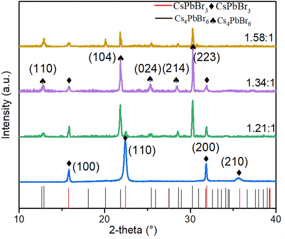 | ||
| Fig. 1 XRD patterns of as-deposited films with different molar ratios. | ||
Further examination was conducted on the optical properties of the four films at different ratios. The PL spectra Fig. 2 illustrate that as the Cs/Pb ratio ranged from 1:1 to 1.58:1, the luminescence peak shifted from 520 nm to 508 nm. Concurrently, the film luminescence changed from green to cyan. We speculate that when the composites incorporate a larger proportion of CsBr, according to the XRD patterns, a high CsBr/PbBr2 ratio generally yields high content of Cs4PbBr6, the Cs-rich Cs4PbBr6 phase possesses a 0D structure with [PbBr6]4− octahedra completely isolated by Cs+ cations, which can serve as a barrier to break the connectivity of [PbBr6]4− in CsPbBr3 and impede the growth of CsPbBr3, the spatial confinement effect is enhanced resulting in the decrease of CsPbBr3 grain size, causing a blue shift in the PL peak position.18 This suggests that the electrons and holes formed in CsPbBr3 are spatially constrained by Cs4PbBr6, resulting in enhanced PL.36 The strongest PL intensity was observed at a Cs/Pb ratio of 1.34, time-resolved photoluminescence (TRPL) spectra are shown in Fig. S1,† suggesting superior optoelectronic quality and high radiative recombination rate in these films. The ultraviolet-visible absorption spectra in Fig. 3 exhibited two absorption peaks at 317 nm and 514 nm, ascribed to Cs4PbBr6 and CsPbBr3, respectively. A progressive increase in the intensity of the absorption band at 317 nm was observed as the Cs/Pb ratio rose from 1.21 to 1.58, which implies an increase in the Cs4PbBr6 phase content within the nanocomposite corresponding to the increased CsBr content in the precursor.
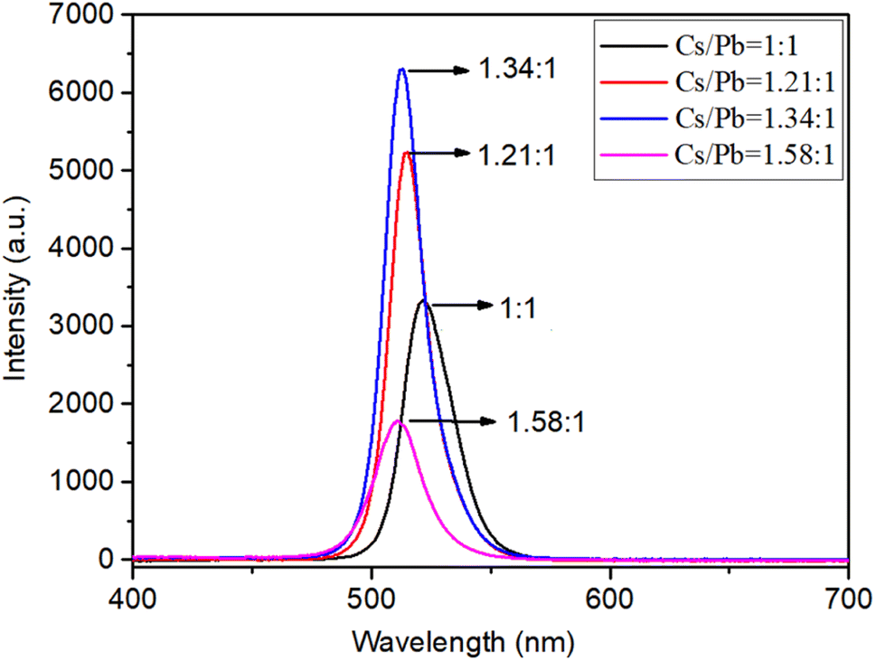 | ||
| Fig. 2 PL spectra of Cs–Pb–Br films with different molar ratios. | ||
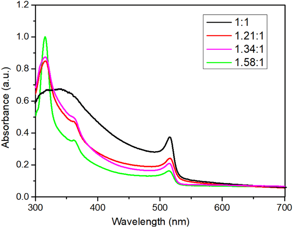 | ||
| Fig. 3 The absorption spectra of Cs–Pb–Br films with different molar ratios. | ||
Surface morphologies of the CsPbBr3 and CsPbBr3–Cs4PbBr6 composite films were further investigated using SEM. As shown in Fig. 4, the films appear dense and devoid of pinholes, featuring two distinct grain morphologies as the Cs/Pb ratio increases. A transmission electron microscopy (TEM) image (Fig. 5(a)) of a specimen made by scraping a Cs/Pb = 1:1 thin film exhibited the similar cubic CsPbBr3 structure, and on further increasing the molar ratio to Cs/Pb = 1.34/1 reveals that two crystal morphologies appear in the image (Fig. 5(b)). The larger rhombic shaped crystal with smooth outer surface and almost sharp edges (crystal size of about 187 nm) and the cubic shaped CsPbBr3 small grains with an average size of 54 nm, which is similar to the previously reported TEM results for the CsPbBr3/Cs4PbBr6 material.37 Therefore, a high-resolution TEM (HR-TEM) image was acquired to identify the rhombic shaped phase. Fig. 6(c) shows a HR-TEM image exhibiting different sets of lattice fringes, which can be attributed to the CsPbBr3 and Cs4PbBr6 phases. Fig. 6(c) exhibited a lattice spacing of 0.56 nm in inner layer, which is consistent with the (100) crystal plane, confirming the cubic CsPbBr3 structure. As for grain edges, a lattice spacing of 0.41 nm, corresponding to the (104) crystal plane, confirming the rhombohedral Cs4PbBr6 structure. Therefore, the HR-TEM results demonstrate that CsPbBr3 are embedding into the rhombohedral prism of the Cs4PbBr6 structure, forming core–shell CsPbBr3/Cs4PbBr6 structure. The energy-dispersive spectroscopy (EDS) in Fig. 6(b) confirm the conclusion. Due to the existence of the thin shell layer, size of the CsPbBr3 would reduce resulting in a blue shift,38 this is consistent with PL spectra and SEM images.
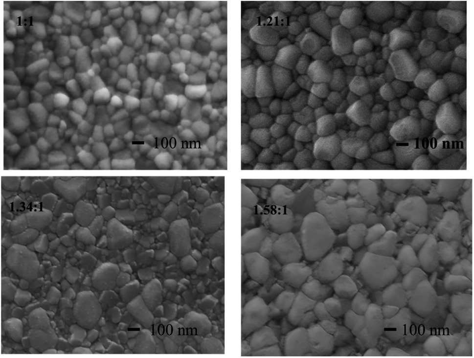 | ||
| Fig. 4 SEM images of as-deposited films with different molar ratios. | ||
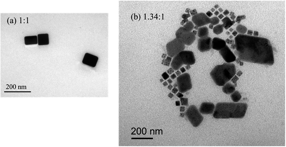 | ||
| Fig. 5 TEM images of (a) 1:1 thin film (b) 1.34:1 thin film. | ||
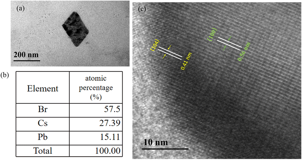 | ||
| Fig. 6 (a) TEM images of (b) element atomic percentage of (c) HR-TEM images of CsPbBr3–Cs4PbBr6 core–shell structure. | ||
Based on the results obtained from PL spectra and XRD patterns, it is evident that the films exhibit high photoluminescence intensity and good crystalline quality when the Cs/Pb ratio is 1.34. With the increasing Cs/Pb ratio, the film luminescence changes from green to cyan due to the shift of the luminescence peak position, which deviates from our desired luminescence color. In addition, too much CsBr leads to the water instability of CsPbBr3–Cs4PbBr6 film. Therefore, for further study and the fabrication of electroluminescent devices, we focus on the film with a CsBr/PbBr2 ratio of 1.34.
3.2. Effect of air-annealing temperature on the CsPbBr3–Cs4PbBr6 films
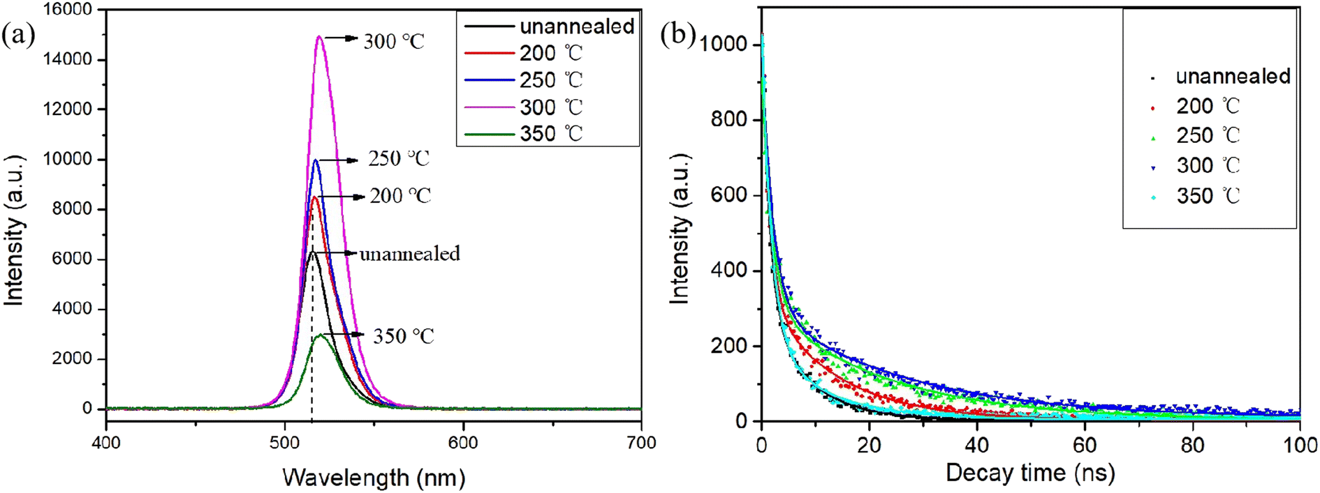
In order to further improve the crystalline quality of the films and reduce the defect concentration, we employed rapid thermal annealing on CsPbBr3–Cs4PbBr6 films (with a Cs/Pb ratio of 1.34) in an ambient air atmosphere. This allowed us to observe the effect of various annealing temperatures (ranging from 200 °C to 350 °C) on the luminescence properties and crystallinity of the films.Fig. 7(a) illustrates the photoluminescence (PL) spectra of the annealed composite films at different temperatures. For the annealed samples, it is observed that as the annealing temperature increases, the PL intensity strengthens constantly. The strongest PL intensity is observed in the CsPbBr3–Cs4PbBr6 film annealed at 300 °C, indicating that the film has the best photoluminescence with lower defects. After that, the PL intensity decreases as the annealing temperature continues to increase. In addition, the PL emission peaks of the annealed samples exhibit a red shift as the annealing temperature increases, in comparison to the unannealed films. This may be attributed to the increase in grain size.
 | ||
| Fig. 7 (a) PL spectra (b) time-resolved photoluminescence (TRPL) spectra at different annealing temperatures. | ||
Fig. 7(b) exhibits the time-resolved photoluminescence (TRPL) spectra of the films at different annealing temperatures and a double exponential fit to the PL lifetime. The deduced decay lifetimes are shown in Table S2.† Typically, the slow decay (τ2) component represents the process of trap-assisted radiative recombination within the bulk perovskite phase, while the fast decay (τ1) component reflects the carrier quenching at the interface.39 The recombination lifetimes of both the surface and bulk phase of the annealed films were substantially prolonged, from 1.41 ns and 6.34 ns to 2.02 ns and 26.24 ns, respectively. When compared to the unannealed films, this signifies a significant reduction in both the surface defect density and bulk phase defect density of the films.40
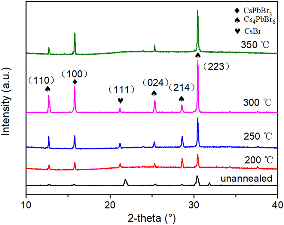
The XRD patterns of the CsPbBr3–Cs4PbBr6 films at different annealing temperatures are depicted in Fig. 8. We noted the disappearance of the (104) crystal plane of Cs4PbBr6 and the appearance of the (111) crystal plane, correlating to the CsBr phase (PDF#78-0615), with the increase in annealing temperature. Also with the increase of annealing temperature, the diffraction intensity of the (100) crystal plane corresponding to CsPbBr3 increases continuously below 300 °C, while the FWHM of the diffraction peak becomes narrower, and the grain size of CsPbBr3 increases according to the Debye–Scherrer formula. This is likely a consequence of the gradual decomposition of Cs4PbBr6 into CsPbBr3 and CsBr under the influence of ambient humidity, relevant to the reaction process Cs4PbBr6 → CsPbBr3 + 3CsBr. During this process, the decomposed CsPbBr3 grains and the Cs4PbBr6 internal CsPbBr3 grains continue to fuse and grow, and the crystallinity tends to be complete,41,42 eventually leading to enhanced fluorescence. This is also consistent with the conclusion obtained from PL spectra. The diffraction peak intensity of (100) and (223) crystal plane reaches the highest at 300 °C. This implies a superior crystalline quality of the film at this temperature.
 | ||
| Fig. 8 XRD patterns of the films at different annealing temperatures. | ||
Fig. 9 presents the surface morphologies of the CsPbBr3–Cs4PbBr6 thin films annealed at varying temperatures and the grain size distribution statistics are shown in Fig. S2.† All the samples are uniform and dense, and the surface is fully covered. When the initial annealing temperature is low, the grain size increase is limited, and the grain boundaries become blurred. When the annealing temperature reaches 300 °C, the CsPbBr3 grains located inside Cs4PbBr6 keep growing, the crystallinity tends to be complete,34 the thin films become more dense, and the crystalline quality improves, which is beneficial to the device performance. This is consistent with the XRD observation. Therefore, we believe that CsPbBr3 is embedded in the host Cs4PbBr6 and the annealing process is always accompanied by the growth and crystalline improvement of CsPbBr3.
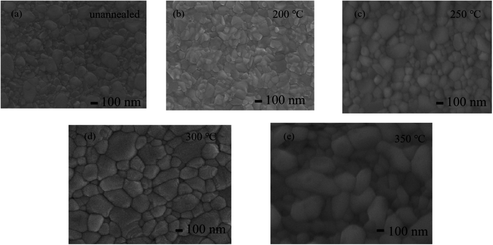 | ||
| Fig. 9 SEM images of films annealed at different temperatures (a) unannealed (b) 200 °C (c) 250 °C (d) 300 °C (e) 350 °C. | ||
3.3. Effect of air-annealing time on the CsPbBr3–Cs4PbBr6 films
We further investigated the impact of annealing conditions, including temperature and time, on CsPbBr3–Cs4PbBr6. Fig. 10(a) shows the PL spectra of the films after annealing at 300 °C for 40–100 s in an ambient atmosphere. As the annealing time is extended, the PL intensity initially increases, peaking at 60 s, before declining. This indicates that the proper annealing time is beneficial to the luminescence of the films. Meanwhile, the films at 60 s have longer surface and bulk phase combination lifetimes compared with other annealing times, as shown in Fig. 10(b). The deduced decay lifetimes are shown in Table S3,† τ1 and τ2 were significantly prolonged from 1.1 ns and 6.94 ns to 2.02 ns and 26.24 ns, respectively.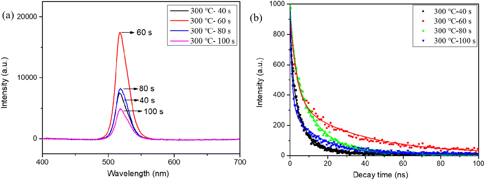 | ||
| Fig. 10 (a) PL spectra (b) time-resolved photoluminescence (TRPL) spectra at different annealing times. | ||
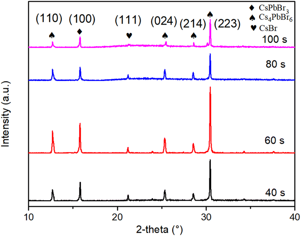
The XRD patterns of the films, presented in Fig. 11, reveal that as the annealing time increases, the intensity of the (100) and (223) crystal plane diffraction peak is the strongest at 60 s, indicating a good crystallinity at this time, and a proper annealing time is favorable for the luminescence and crystallinity.
 | ||
| Fig. 11 XRD patterns of the films at different annealing times. | ||
SEM images of the films at different annealing times are presented in Fig. 12 and the domain size distribution histograms are shown in Fig. S3.† As the annealing time increases, the small grains corresponding to CsPbBr3 grow together with Cs4PbBr6 grains and the grain size keeps increasing. However, with the further prolongation of annealing time, the film grains decompose and holes appear in the film leading to a decrease in crystallinity. The appropriate annealing time enhances the luminescence due to the improvement of crystal quality and the reduction of defects,29 but the large grains produced by the excessively long annealing time lead to weakened carrier confinement and reduced luminescence intensity.13 Consequently, the optimal annealing condition for CsPbBr3–Cs4PbBr6 films is determined to be 60 s at 300 °C. This condition yields the strongest PL intensity and the highest crystallinity.
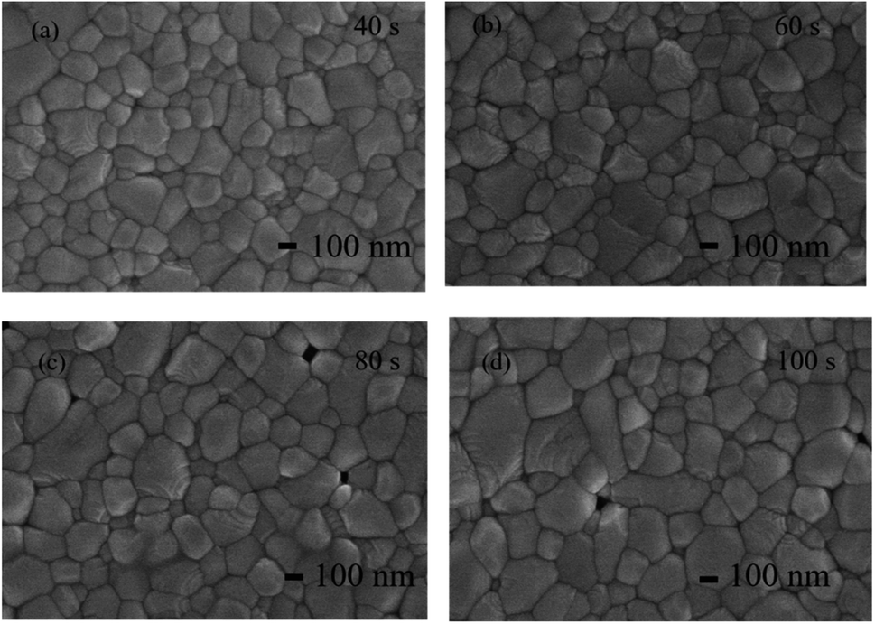 | ||
| Fig. 12 SEM images of films annealed at 300 °C for different time (a) 40 s (b) 60 s (c) 80 s (d) 100 s. | ||
3.4. Research on the stability of CsPbBr3–Cs4PbBr6 thin films
The stability of the as-deposited and annealed CsPbBr3–Cs4PbBr6 thin films were assessed by monitoring the attenuation of PL intensity in an ambient air environment at 48% relative humidity (RH), as depicted in Fig. 13(a) and (b). The images and surface morphology of the unannealed and annealed film after being placed in the air for 150 days are shown in Fig. S4 and S5.† Fig. 13(c) reveals that during the first 50 days of storage, a significant decay ∼40% in PL intensity was observed in unannealed film, however, the PL strength of the annealed film only attenuated by 12%. Over the following 50 days, the annealed film showed no significant decay in PL intensity. This could be due to annealing for improved crystallization quality and reduced defects. Meanwhile, sufficient passivation of the surface, which protected CsPbBr3 from PL quenching. Environmental stability experiment showed the annealed film ∼15% of the PL intensity loss after storage in ambient conditions for 100 days, signifying that the annealed films exhibit excellent environmental stability.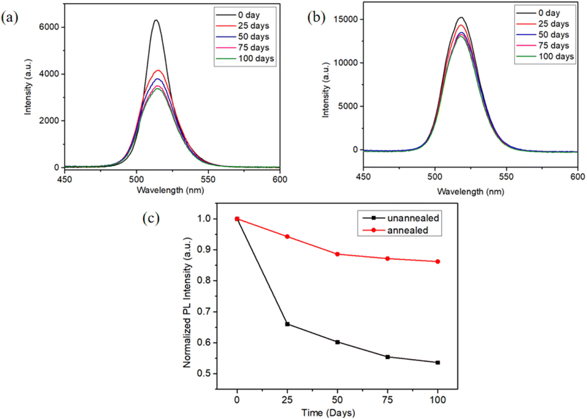 | ||
| Fig. 13 (a) Peak positions of PL spectra of unannealed films, (b) peak positions of PL spectra of annealed films at different storage times in ambient air (λex = 325 nm) (b) the PL intensity trend. | ||
3.5. Study on the PeLEDs
Last, based on the best crystallinity and morphology, with the optimized parameters (Cs/Pb ratio of 1.34/1; perovskite film's thickness of 180 nm; annealing temperature of 300 °C with 60 s); we fabricated Perovskite light emitting diodes (PeLEDs) devices with the architecture of Ag/N–Si/CsPbBr3–Cs4PbBr6/NiO/ITO. The devices architecture is shown in Fig. 14(a). The perovskite CsPbBr3–Cs4PbBr6 layer serves as the emitting layer of carrier radiation recombination. The working mechanism of the device can be elucidated according to the fundamental physical processes of light-emitting diodes.43,44 Driven by forward voltage, green electroluminescence of the device is observed under dark conditions, the PeLEDs show good rectification characteristics, with small reverse current and the turn-on voltage of the device is ∼3 V. Fig. 14(b) presents the electroluminescence (EL) spectrum of the devices, with an inset showing a photograph of our PeLEDs at an injection voltage of 10 V. The spectra shows an emission peak at 517 nm with the FWHM of 16 nm, indicating that our PeLEDs possess excellent color purity. Furthermore, devices with annealed CsPbBr3–Cs4PbBr6 films exhibit higher EL intensity compared to the unannealed films, which indicates that the enhancement of films quality and device performance by rapid annealing in ambient air. After annealing, the devices performed best with a maximum luminance (Lmax) of 957 cd m−2. Importantly, our unencapsulated PeLEDs operate continuously for 12 hours under direct current drive with only a 10% attenuation in ambient air conditions, demonstrating their relatively superior stability in Fig. 15. Compared to reference devices using traditional organic carrier injection layers such as PEDOT:PSS,45 our device provides significantly improved operational stability.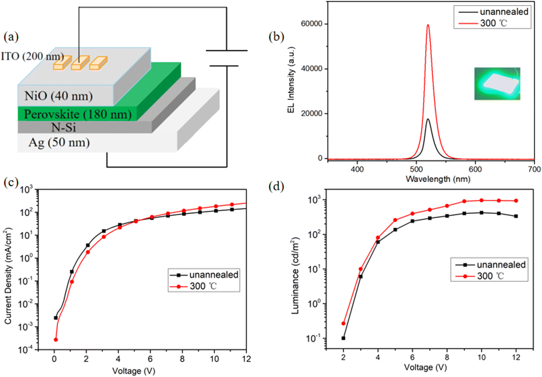 | ||
| Fig. 14 (a) The devices architecture, (b) EL spectra, the insets show the photograph of the PeLEDs at an injection voltage of 10 V, (c) current density against voltage (J–V) curves of PeLEDs and (d) luminance against voltage (L–V) curves. | ||
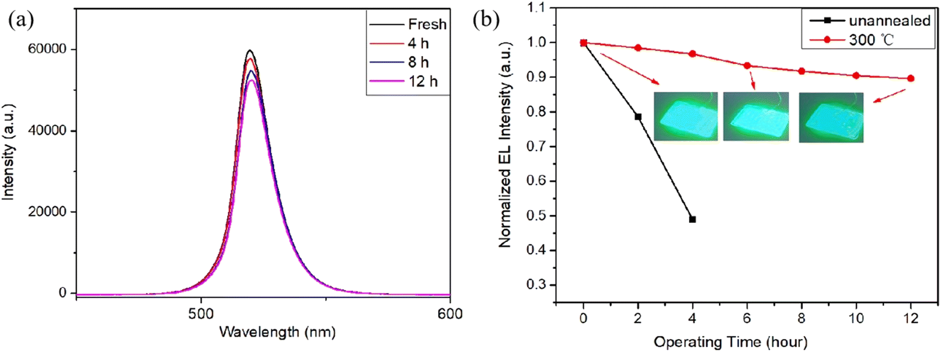 | ||
| Fig. 15 (a) EL spectra acquired at different operating cycles under the same dc bias of 8 V and measurement conditions. (b) The EL intensity trend, the insets show the corresponding photographs of the PeLED after different running periods. | ||
4. Conclusion
In conclusion, high quality CsPbBr3–Cs4PbBr6 films were successfully prepared via a co-evaporation method, guided by the careful adjustment of the CsBr/PbBr2 molar ratio. The enhancement in the optical properties and stability of the films was observed with an increase in Cs/Pb ratio, with the optimal ratio found to be 1.34/1. A luminescence peak near 515 nm was identified in the films with a narrow FWHM An air rapid annealing treatment was utilized to further improve the films' crystalline quality. The optimal PL intensity and crystalline quality were achieved at an annealing temperature of 300 °C for 60 s. These annealed films exhibited excellent stability, maintaining 85% of their PL intensity after 100 days in ambient air conditions. Based on these films, we constructed all-inorganic structured PeLEDs (Ag (50 nm)/N–Si/CsPbBr3–Cs4PbBr6 (180 nm)/NiO (40 nm)/ITO (200 nm)), the unencapsulated device showed only a 10% decay after 12 h, under ambient air condition. This work presents a promising approach for future design and development of stable perovskite-based LEDs.Data availability
All data generated or analysed during this study are included in this published article.Conflicts of interest
The authors declare that they have no competing interests.Author contributions
Tianxinyu Bai wrote the main manuscript. Shenwei Wang, Kexin Zhang and Chunyang Chu, Yingqiang Sun read and approved the final manuscript. Lixin Yi: funding acquisition.Acknowledgements
This study was supported in part by grants from the National Natural Science Foundation of China (Grant No. 61975008). It was also supported by the Key Laboratory of Luminescence and Optical Information of China in Beijing Jiaotong University.References
- C. Tian, K. Lin, J. Lu, W. Feng, P. Song, L. Xie and Z. Wei, Small Methods, 2020, 4, 1900476 CrossRef CAS
.
- Y. Kim, H. Cho, J. H. Heo, T. Kim, N. Myoung, C. Lee, S. H. Im and T. Lee, Adv. Mater., 2015, 27, 1248–1254 CrossRef CAS PubMed
- Z. Xiao, R. A. Kerner, L. Zhao, N. L. Tran, K. M. Lee, T. Koh, G. D. Scholes and B. P. Rand, Nat. Photonics, 2017, 11, 108–115 CrossRef CAS
- J. Xue, R. Wang, X. Chen, C. Yao, X. Jin, K. Wang, W. Huang, T. Huang, Y. Zhao, Y. Zhai, D. Meng, S. Tan, R. Liu, Z. Wang, C. Zhu, K. Zhu, M. C. Beard, Y. Yan and Y. Yang, Science, 2021, 371, 636–640 CrossRef CAS PubMed
- Q. Gao, J. Qi, K. Chen, M. Xia, Y. Hu, A. Mei and H. Han, Adv. Mater., 2022, 34, 2200720 CrossRef CAS PubMed
- J. S. Kim, J. Heo, G. Park, S. Woo, C. Cho, H. J. Yun, D. Kim, J. Park, S. Lee, S. Park, E. Yoon, N. C. Greenham and T. Lee, Nature, 2022, 611, 688–694 CrossRef CAS PubMed
- K. Jia, L. Song, Y. Hu, X. Guo, X. Liu, C. Geng, S. Xu, R. Fan, L. Huang, N. Luan and W. Bi, ACS Appl. Mater. Interfaces, 2020, 12, 15928–15933 CrossRef CAS PubMed
- W. Li, Y. Xu, D. Wang, F. Chen and Z. Chen, Org. Electron., 2018, 57, 60–67 CrossRef CAS
- J. Lei, F. Gao, H. Wang, J. Li, J. Jiang, X. Wu, R. Gao, Z. Yang and S. F. Liu, Sol. Energy Mater. Sol. Cells, 2018, 187, 1–8 CrossRef CAS
- D. Zhao, W. Ke, C. R. Grice, A. J. Cimaroli, X. Tan, M. Yang, R. W. Collins, H. Zhang, K. Zhu and Y. Yan, Nano Energy, 2016, 19, 88–97 CrossRef CAS
- J. Liang, C. Wang, Y. Wang, Z. Xu, Z. Lu, Y. Ma, H. Zhu, Y. Hu, C. Xiao, X. Yi, G. Zhu, H. Lv, L. Ma, T. Chen, Z. Tie, Z. Jin and J. Liu, J. Am. Chem. Soc., 2016, 138, 15829–15832 CrossRef CAS PubMed
- X. Hu, X. Zhang, L. Liang, J. Bao, S. Li, W. Yang and Y. Xie, Adv. Funct. Mater., 2014, 24, 7373–7380 CrossRef CAS
- Y. Fu, Q. Zhang, D. Zhang, Y. Tang, L. Shu, Y. Zhu and Z. Fan, Adv. Funct. Mater., 2020, 30, 2002913 CrossRef CAS
- L. Chu, W. Ahmad, W. Liu, J. Yang, R. Zhang, Y. Sun, J. Yang and X. A. Li, Nano-Micro Lett., 2019, 11, 16 CrossRef PubMed
- S. Woo, J. S. Kim and T. Lee, Nat. Photonics, 2021, 15, 630–634 CrossRef CAS
- J. Lin and T. Wang, Sol. Energy Mater. Sol. Cells, 2022, 3, 3–4 Search PubMed
- G. Hu, W. Qin, M. Liu, X. Ren, X. Wu, L. Yang and S. Yin, J. Mater. Chem. C, 2019, 7, 4733–4739 RSC
- P. Du, L. Wang, J. Li, J. Luo, Y. Ma, J. Tang and T. Zhai, Adv. Opt. Mater., 2022, 10, 2101770 CrossRef CAS
- P. Du, J. Li, L. Wang, L. Sun, X. Wang, X. Xu, L. Yang, J. Pang, W. Liang, J. Luo, Y. Ma and J. Tang, Nat. Commun., 2021, 12, 4751 CrossRef CAS PubMed
- Q. A. Akkerman, S. Park, E. Radicchi, F. Nunzi, E. Mosconi, F. De Angelis, R. Brescia, P. Rastogi, M. Prato and L. Manna, Nano Lett., 2017, 17, 1924–1930 CrossRef CAS PubMed
- X. Xiong, H. Liu, W. Wang, J. Gong, X. Chen, Y. Zhao, T. Tian and L. Wang, Luminescence, 2021, 36, 631–641 CrossRef CAS PubMed
- L. Wang, H. Liu, Y. Zhang and O. F. Mohammed, ACS Energy Lett., 2020, 5, 87–99 CrossRef CAS
- Z. Ma, Z. Liu, S. Lu, L. Wang, X. Feng, D. Yang, K. Wang, G. Xiao, L. Zhang, S. A. T. Redfern and B. Zou, Nat. Commun., 2018, 9, 4506 CrossRef PubMed
- Z. Wang, Y. Zhang, X. Liu, Y. Yu, F. Xu, J. Ding, X. Liang, K. Yang and W. Xiang, Adv. Mater. Technol., 2021, 6, 2100654 CrossRef CAS
- X. Lian, X. Wang, Y. Ling, E. Lochner, L. Tan, Y. Zhou, B. Ma, K. Hanson and H. Gao, Adv. Funct. Mater., 2019, 29, 1807345 CrossRef
- J. Li, P. Du, S. Li, J. Liu, M. Zhu, Z. Tan, M. Hu, J. Luo, D. Guo, L. Ma, Z. Nie, Y. Ma, L. Gao, G. Niu and J. Tang, Adv. Funct. Mater., 2019, 29, 1903607 CrossRef CAS
- Y. Hu, Q. Wang, Y. Shi, M. Li, L. Zhang, Z. Wang and L. Liao, J. Mater. Chem. C, 2017, 5, 8144–8149 RSC
- T. Bai, S. Wang, L. Bai, K. Zhang, C. Chu and L. Yi, Nanoscale Res. Lett., 2022, 17, 69 CrossRef CAS PubMed
- L. Y. Bai, S. W. Wang, Y. W. Zhang, K. X. Zhang and L. X. Yi, J. Lumin., 2020, 227, 117592 CrossRef CAS
- H. Li, G. Tong, T. Chen, H. Zhu, G. Li, Y. Chang, L. Wang and Y. Jiang, J. Mater. Chem. A, 2018, 6, 14255–14261 RSC
- J. Cao, X. Zeng, W. Li, L. Lv, C. Yan, H. Huang, J. Lu and W. Yang, Appl. Mater. Today, 2023, 30, 101733 CrossRef
- T. Chen, C. Wang and J. Bao, 2021 IEEE 16th Nanotechnology Materials and Devices Conference (NMDC), 2021, pp.1–5 Search PubMed
- X. Lian, X. Wang, Y. Ling, E. Lochner, L. Tan, Y. Zhou, B. Ma, K. Hanson and H. Gao, Adv. Funct. Mater., 2019, 29, 1807345 CrossRef
- K. Lin, C. Yan, R. P. Sabatini, W. Feng, J. Lu, K. Liu, D. Ma, Y. Shen, Y. Zhao, M. Li, C. Tian, L. Xie, E. H. Sargent and Z. Wei, Adv. Funct. Mater., 2022, 32, 2200350 CrossRef CAS
- H. Cho, S. Jeong, M. Park, Y. Kim, C. Wolf, C. Lee, J. H. Heo, A. Sadhanala, N. Myoung, S. Yoo, S. H. Im, R. H. Friend and T. Lee, Science, 2015, 350, 1222–1225 CrossRef CAS PubMed
- M. Jo, N. Yasuhara, K. Ishida, K. Kawamoto and S. Fukatsu, Phys. E, 2004, 21, 354–357 CrossRef CAS
- V. Naresh, T. Jang, Y. Pang and N. Lee, Nanoscale, 2022, 14, 17789–17801 RSC
- J. Xu, W. Huang, P. Li, D. R. Onken, C. Dun, Y. Guo, K. B. Ucer, C. Lu, H. Wang, S. M. Geyer, R. T. Williams and D. L. Carroll, Adv. Mater., 2017, 29, 1703703 CrossRef PubMed
- D. Shi, V. Adinolfi, R. Comin, M. Yuan, E. Alarousu, A. Buin, Y. Chen, S. Hoogland, A. Rothenberger, K. Katsiev, Y. Losovyj, X. Zhang, P. A. Dowben, O. F. Mohammed, E. H. Sargent and O. M. Bakr, Science, 2015, 347, 519–522 CrossRef CAS PubMed
- L. Liu, S. Yang, P. Liu and Y. Chen, Sol. Energy, 2022, 232, 320–327 CrossRef CAS
- Y. Ling, L. Tan, X. Wang, Y. Zhou, Y. Xin, B. Ma, K. Hanson and H. Gao, J. Phys. Chem. Lett., 2017, 8, 3266–3271 CrossRef CAS PubMed
- X. Xiong, H. Liu, W. Wang, J. Gong, X. Chen, Y. Zhao, T. Tian and L. Wang, Luminescence, 2021, 36, 631–641 CrossRef CAS PubMed
- S. Zhuang, X. Ma, D. Hu, X. Dong and B. Zhang, Ceram. Int., 2018, 44, 4685–4688 CrossRef CAS
- B. Liu, L. Wang, H. Gu, H. Sun and H. V. Demir, Adv. Opt. Mater., 2018, 6, 1800220 CrossRef
- U. Kwon, B. Kim, D. C. Nguyen, J. Park, N. Y. Ha, S. Kim, S. H. Ko, S. Lee, D. Lee and H. J. Park, Sci. Rep., 2016, 6, 30759 CrossRef CAS PubMed
Footnote |
| † Electronic supplementary information (ESI) available. See DOI: https://doi.org/10.1039/d3ra03947a |
| This journal is © The Royal Society of Chemistry 2023 |