
 Open Access Article
 This Open Access Article is licensed under a Creative Commons Attribution-Non Commercial 3.0 Unported Licence
Anisotropic crystal orientations dependent mechanical properties and fracture mechanisms in zinc blende ZnTe nanowires†
A. S. M. Jannatul Islam a,
Md. Sherajul Islam*a,
Md. Sayed Hasana,
Kamal Hosenb,
Md. Shahadat Akbara,
Ashraful G. Bhuiyana and
Jeongwon Parkcd
a,
Md. Sherajul Islam*a,
Md. Sayed Hasana,
Kamal Hosenb,
Md. Shahadat Akbara,
Ashraful G. Bhuiyana and
Jeongwon Parkcd
aDepartment of Electrical and Electronic Engineering, Khulna University of Engineering &Technology, Khulna 9203, Bangladesh. E-mail: sheraj_kuet@eee.kuet.ac.bd
bDepartment of Electrical and Computer Engineering, University of Minnesota Twin Cities, Minneapolis, MN 55455, USA
cDepartment of Electrical and Biomedical Engineering, University of Nevada, Reno, NV 89557, USA
dSchool of Electrical Engineering and Computer Science, University of Ottawa, Ottawa, ON K1N 6N5, Canada
First published on 27th July 2023
Abstract
The orientations of crystal growth significantly affect the operating characteristics of elastic and inelastic deformation in semiconductor nanowires (NWs). This work uses molecular dynamics simulation to extensively investigate the orientation-dependent mechanical properties and fracture mechanisms of zinc blende ZnTe NWs. Three different crystal orientations, including [100], [110], and [111], coupled with temperatures (100 to 600 K) on the fracture stress and elastic modulus, are thoroughly studied. In comparison to the [110] and [100] orientations, the [111]-oriented ZnTe NW exhibits a high fracture stress. The percentage decrease in fracture strength exhibits a pronounced variation with increasing temperature, with the highest magnitude observed in the [100] direction and the lowest magnitude observed in the [110] direction. The elastic modulus dropped by the largest percentage in the [111] direction as compared to the [100] direction. Most notably, the [110]-directed ZnTe NW deforms unusually as the strain rate increases, making it more sensitive to strain rate than other orientations. The strong strain rate sensitivity results from the unusual short-range and long-range order crystals appearing due to dislocation slipping and partial twinning. Moreover, the {111} plane is the principal cleavage plane for all orientations, creating a dislocation slipping mechanism at room temperature. The {100} plane becomes active and acts as another fundamental cleavage plane at increasing temperatures. This in-depth analysis paves the way for advancing efficient and reliable ZnTe NWs-based nanodevices and nanomechanical systems.
1. Introduction
One-dimensional nanostructures, such as nanowires (NWs) and nanorods, are the focus of much research interest due to their unique features and great potential in several technological applications ranging from optoelectronics to biology.1–3 Over the past few years, numerous NWs from II–VI, III–V, and IV–VI group semiconductors have been developed, which include GeSn, CdSe, ZnS, ZnSe, ZnTe, InP, GaN, and SiC.4–11 In particular, ZnTe NW is of special importance owing to its exceptional electrical, thermal, and optical characteristics as well as the potential for use in nanoelectromechanical systems (NEMS) such as nanoresonators, nanogenerators, and nano-cantilever sensors.3,12–18 Zinc blende (ZB) ZnTe NWs19–21 have three different crystallographic orientations along the growth axis, namely [100], [110], and [111], which can affect their physical properties, including bandgap, surface reactivity, piezoelectric polarization, index of refraction, and electrical and thermal conductivity.22–24 The side surfaces are dissimilar for these three different growth directions. These side surfaces can considerably affect the mechanical behavior and fracture process through partial slipping, full slipping, necking, and/or twinning.25–28 Recent experimental22,29 and theoretical studies8,9 also suggest that different crystal orientations of NWs can exhibit considerable anisotropic mechanical properties with temperature and strain. The competition between global and local deformations, activation variation in different planes, and the influence disparity of inter-planar distances may change with temperature and strain rate,30–35 leading to this anisotropic behavior. A thorough knowledge of the crystal orientation-dependent mechanical characteristics is thus an essential requirement for the development of further technological applications of this nanostructure.The thermal, electrical, optical, structural, and lattice dynamical behaviors of ZnTe nanostructures have been extensively studied in recent years using ab initio simulations and other techniques.14,15,36,37 Despite extensive theoretical and practical investigations into the electronic, thermal, and optical characteristics of ZnTe NWs, there is a lack of literature exploring the influence of crystal direction on the tensile deformation behavior. Further investigation is required to enhance our understanding of the influence of environmental factors, such as temperature and strain rate, on mechanical strength. To effectively utilize ZnTe NWs in various NEMS and nanodevices, particularly those reliant on mechanical responses to achieve desired functionalities, it is imperative to obtain a comprehensive assessment of their mechanical properties and failure mechanisms. Moreover, the challenges associated with sample preparation, intricate surface morphology, and the small dimensions of the NWs pose difficulties in accurately clamping and aligning the axial orientation of the NWs with the loading direction.38
In this work, we have comprehensively investigated the atomistic deformation mechanisms and the tensile mechanical properties of ZB ZnTe NWs, with a particular focus on the three different crystal directions ([100], [110], and [111]) through molecular dynamics (MD) simulation. The Stillinger–Weber (SW) potential introduced by Zhou et al.39 was employed to characterize the interatomic interactions of the systems. To verify the effect of crystal orientation coupled with temperatures (100 to 600 K) and strain rate (1 × 10⁸ s−1 to 1 × 10¹⁰ s−1) on mechanical strength, we have explored the radial distribution function (RDF), potential energy per atom (PE/atom), and deformation images. We believe that our research will pave the way for a complete knowledge of the mechanical characteristics and deformation mechanisms of ZB ZnTe NWs and practical applications of ZnTe-based nanodevices and NEMS.
2. Computational details
At first, ZB ZnTe NWs with [100], [110], and [111] crystallographic growth orientations have been created, as depicted in Fig. 1. The interatomic relations between Zn–Te, Zn–Zn, and Te–Te have been defined by the SW potential.39 All four faces of a [100]-oriented NW are of the {100} type (Fig. 1a). The [110]-oriented NW is surrounded by two {112} and two {111} sides (Fig. 1b), while the [111]-oriented NW contains two {112} and two {110} as its side faces (Fig. 1c). Previous research agrees with the structures of all different ZB ZnTe NWs with different surfaces.10,32 The constrained scale of the atomistic simulations necessitates a deliberate selection of size to facilitate a significant comprehension of the deformation behavior. Here, a lattice constant of a = 6.1026 Å has been chosen to form a rectangular ZB ZnTe box with different orientations using the Atomsk tool.40 We have then transformed it into rectangular nanopillar structures, or NWs, with a length-to-width ratio of 8![[thin space (1/6-em)]](https://www.rsc.org/images/entities/char_2009.gif) :1, comprising 21952 to 23040 atoms and having the following dimensions: 34.17 nm × 4.27 nm × 4.27 nm.30,38 Each NW is positioned in the middle of a cuboid-shaped vacuum box with border lengths equivalent to 10 nm + NW structure length + 10 nm in both the y and z directions. It should be noted that the side length of the box along the x-axis is chosen as the length of the NWs. The periodic boundary condition (BC) is employed in the longitudinal axis, while the static BC is employed in the additional two directions. It has been found that the box side lengths (10 nm on both sides) along the y- and z-axes are sufficient to prevent any abnormal interactions between nearby NWs and to provide enough area for the NWs to deform easily.
:1, comprising 21952 to 23040 atoms and having the following dimensions: 34.17 nm × 4.27 nm × 4.27 nm.30,38 Each NW is positioned in the middle of a cuboid-shaped vacuum box with border lengths equivalent to 10 nm + NW structure length + 10 nm in both the y and z directions. It should be noted that the side length of the box along the x-axis is chosen as the length of the NWs. The periodic boundary condition (BC) is employed in the longitudinal axis, while the static BC is employed in the additional two directions. It has been found that the box side lengths (10 nm on both sides) along the y- and z-axes are sufficient to prevent any abnormal interactions between nearby NWs and to provide enough area for the NWs to deform easily.
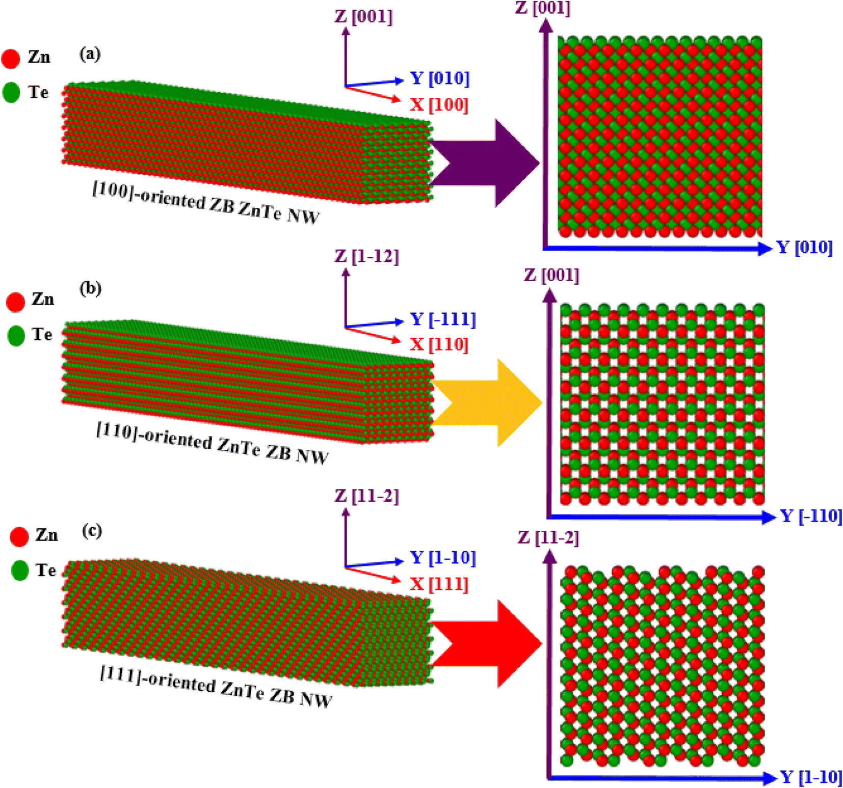 | ||
| Fig. 1 Initial structure of the (a) [100]-directed (b) [110]-directed and (c) [111]-directed ZB ZnTe NW with a dimension of 34.17 nm × 4.27 nm × 4.27 nm. The zoomed-in view of the cross-section of each of the NWs is shown on the right side of the figures. | ||
After forming the initial NW, the conjugate gradient technique is applied to minimize the energy of the system. The structure is then relaxed through an NPT ensemble in the x direction for 50 ps. The structure is also thermally optimized utilizing a canonical NVT ensemble for 50 ps. Nose–Hoover thermostat is employed to control the temperature. The velocity Verlet method is applied for a time step of 1 fs to integrate the standard Newton equations of motion over time. After structural relaxation and energy minimization, we applied tensile loading along the length's (x) direction at an identical strain rate of 109 s−1. This strain rate is effective for MD simulations, and it has been successfully applied in numerous works.30,38
Changing the length of the sides of the cuboid box along the x-axis makes it possible to simulate a uniaxial tensile loading. The strain of NWs in the x-direction is changed simultaneously due to the periodic BC (PBC). The engineering strain, or tensile strain, is denoted by the equation ε = ΔL/L0, where ΔL is the deviation of the length from its initial length L0. In our simulations, physical stresses are calculated utilizing the Virial stress theorem,41 which is obtained as the arithmetic mean of the native stresses on all atoms and has the following formula:
 | (1) |
3. Results and discussion
Through numerous growth techniques46–48 such as laser ablation, chemical vapor deposition, and thermal evaporation, NWs can be synthesized in different growth orientations. These dissimilar growth orientations can substantially influence the elastic and inelastic distortion processes of semiconductor NWs.31,49 It is well known that group II–VI and III–V binary semiconductors are highly polarized materials.19,50 Due to this crystal polarity, the [111]-oriented ZnTe NWs show low energy and high symmetry features, and most of the NWs have a tendency to grow in a ZB structure along the [111] orientation.15,19,51 However, because of their excellent crystal superiority and unique physical features, other orientational semiconductor NWs have gained growing interest in basic research and prospective applications.52–54 The selective growth of stacking fault-free ZnTe NWs along [100], [110], and [112] crystal orientations is reported using a variety of growth processes, including molecular beam epitaxy and the vapor–liquid–solid growth processes.55,56 Prior studies also revealed that by maintaining cross-linking among the NWs length, diameter, and growth conditions, NWs can be grown along any of these [110], [100], [112], or [111] four orientations, which are confirmed by X-ray diffraction, photoluminescence spectroscopy, and transmission electron microscopy.52,54,57 Realizing the mechanical properties and fracture behavior of ZnTe NWs grown along the [100], [110], and [111] orientations is thus essential for creating and enhancing their uses in various fields, such as NEMS and nanoelectronics.In this section, we first examine the impact of crystal growth orientation on the stress–strain performance of ZB ZnTe NWs. The stress–strain properties upon application of a uniaxial tension at a strain rate of 109 s−1 in three distinct crystal directions ([100], [110], and [111]) are depicted in Fig. 2a. As seen, the responses primarily consist of elastic and plastic phases. The [111]-oriented ZB ZnTe NW exhibits the greatest fracture stress value at 300 K, while the [100]-oriented NW exhibits the lowest value. It has been reported that CdTe, CdSe, Ni–Co, and InP NWs exhibit similar orientation-dependent fracture stress behavior.30,31,38,58 On the other hand, the [100]-oriented ZB ZnTe NW displays a greater fracture strain than the other two crystal alignments. The requirement for this greater fracture strain to deform the [100]-oriented ZB ZnTe NW will be explained later in this paper.
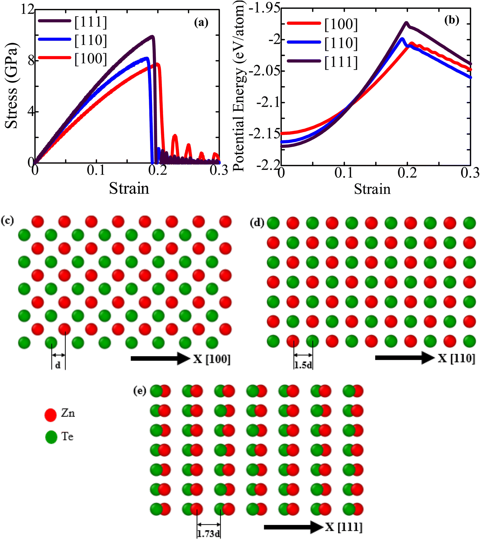 | ||
| Fig. 2 (a) Stress–strain relationship and (b) PE/atomcurves of 18.25 nm2 ZB ZnTe NW for three crystal orientations at 300 K. Demonstrations of atomic assemblies of the ZB ZnTe NW along the orientations of (c) [100] (d) [110] (e) [111] with a relative spacing of Zn2+ and Se2− atoms. | ||
Fracture toughness, the quantity of energy dissipated before failure, can be calculated by evaluating the area underneath the stress–strain curve. The fracture toughness of ZnTe NWs exhibits its highest value when subjected to loading along the [111] crystallographic direction, while its lowest value is observed when loaded along the [100] direction. For each NW, we also graphically computed the elastic modulus using the stress–strain curve's slope (≤1% strain). The small strain zone ensures that the linear elastic destruction occurs and that the structure corresponds to Hook's law. Table 1 shows the predicted elastic modulus for three different crystal growth directions at 300 K. With the highest elastic modulus of ∼64.11 GPa in the [111] direction, the ZnTe NW is extremely rigid, which makes it difficult to deform. The [111] direction exhibits the highest fracture stress and elastic modulus due to its comparatively lower surface energy in comparison to other directions. We compared our calculated elastic modulus of ZB ZnTe NWs at 300 K with the available literature (shown in Table 1).36,42,59,60 The findings demonstrate that the SW interatomic potential can effectively predict the mechanical properties of ZnTe structures with a high degree of accuracy.
The surface zoomed-in view of the ZB ZnTe NWs of three crystal configurations are shown in Fig. 2c–e. In contrast to the [110] and [111]-oriented NW faces, the [100]-oriented NW face (see Fig. 2c) appears to have a very compact structure. For other semiconducting NWs, it has already been proven that the [111] growth direction has the longest surface atomic gap, resulting in a lower number of atoms. This enables it to possess the minimum surface energy.30,38 The [111]-directed NW with the lowest energy has therefore demonstrated the highest mechanical strength compared to the other directions. However, due to the smaller surface atomic distance of the [100]-oriented NW compared to the [111]-oriented NW, the [100] orientation exhibits a higher fracture strain than the [111] orientation. To further represent the surface atomic distance, Fig. 2b displays the PE/atom of ZnTe NWs along three different crystal directions ([111], [110], and [100]). The figure shows that the [111]-oriented NW has less PE/atom at zero strain than the other two directions, indicating more physical stability and strength than the other considered directions.
The stress–strain profiles for different configurations at temperatures varying from 100 to 600 K are shown in Fig. 3a–c. The fracture strength and strain decline dramatically as the temperature rises from 100 to 600 K. Using Fig. 3a–c, we have then computed the fracture stress and elastic modulus at various temperatures, as shown in Fig. 4a and b. The ZnTe NWs are shown to have maximum fracture stresses of ∼7.87 GPa, ∼9.51 GPa, and ∼10.98 GPa along the [100], [110], and [111] orientations, respectively, at a temperature of 100 K. Once the temperature reaches 600 K, the fracture stress decreases to ∼5.85 GPa, ∼7.22 GPa, and ∼8.18 GPa along the [100], [110], and [111] orientations, respectively. Fracture stress in these three directions is dropped by ∼25.63%, ∼24.11%, and ∼25.44% when the temperature increases to 600 K from 100 K. The provided figure illustrates that the NW oriented along the [111] direction exhibits a lower PE/atom at zero strain compared to the other two directions. This observation suggests that the [111]-oriented NW possesses greater physical stability and strength in comparison to the other directions under consideration. The anticipated elastic modulus demonstrates a declining pattern as the temperature increases, similar to the behavior observed in fracture stress. According to Fig. 4b, the elastic modulus decreases along the [100], [110], and [111] directions from ∼45.00 to ∼43.76 GPa, ∼61.07 to ∼58.30 GPa, and ∼65.26 to ∼61.78 GPa, respectively, as the temperature rises from 100 to 600 K. Upon increasing temperature from 100 to 600 K, the elastic modulus decreases in three different directions: 2.76%, 4.53%, and 5.32%. The decrease in modulus of elasticity at elevated temperatures can be attributed to several factors, such as thermal expansion, increased atomic mobility, and accelerated free-volume diffusion at higher temperatures.
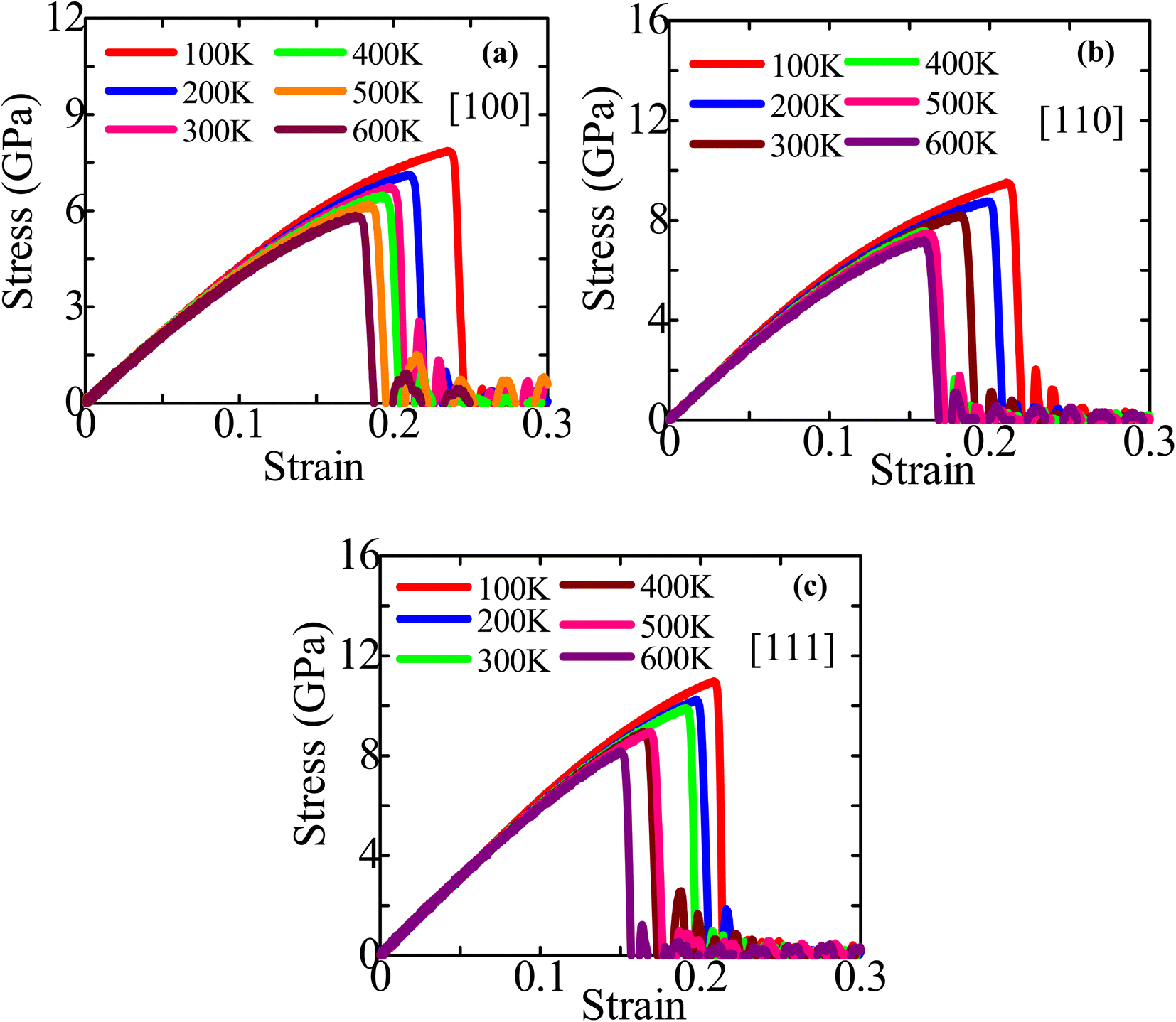 | ||
| Fig. 3 Stress–strain performance curves of (a) [100], (b) [110], and (c) [111]-directed 18.25 nm2 ZB ZnTe NWs at six diverse temperatures. | ||
 | ||
| Fig. 4 Extracted (a) fracture stress and (b) elastic modulus of 18.25 nm2 ZB ZnTe NWs for three dissimilar orientations at diverse temperatures. | ||
The decrease in fracture strength with increasing temperature exhibits the most pronounced effect in the [100] orientation, while the [110] orientation demonstrates the least impact, as depicted in Fig. 4a. In contrast, it can be observed that among three distinct growth directions, the [111] orientation demonstrates the most significant decline in elastic modulus as temperature increases, while the [100] orientation exhibits the least pronounced reduction rate. Subsequently, within the failure mechanism section, an analysis will be presented regarding the deformation behavior of crystal-oriented NWs, elucidating the distinct patterns of fracture stress and elastic modulus reduction observed across different orientations. The total energy per atom (TE/atom) calculation can be employed to define why structural strength declines with rising temperature before tensile strain is applied. Fig. S1a–c (ESI†) depicts the TE/atom profiles of [111], [110], and [100]-directed NWs at six distinct temperatures before the application of a tensile strain. In this work, 50000 MD steps are used to equilibrate all systems. However, only the first 20000 steps for each of the temperatures considered are displayed in the figure. Fig. S1† shows that ZB ZnTe NWs for different crystal orientations appear stably after 1000 steps at all temperatures. However, as the dynamic energy of particles rises with temperature, our computed TE/atom curve also rises. At a temperature of 600 K, all orientations have a higher value, which means that the structure of the ZnTe NWs is less stable than at a temperature of 100 K. As a result, as the temperature rises, less strain energy is required to deform the structure.
The atomic structure experiences considerable lattice vibration due to the temperature rise and the behavior of the spacing lengths between different pairs created in the systems also changes. We have also estimated the RDF, g(r), at three discrete temperatures to qualitatively elucidate the temperature-induced mechanical performance.61–63 The RDFs of Zn–Zn, Zn–Te, and Te–Te pairs in the ZnTe system as a function of temperature are illustrated in Fig. S2a–c (ESI†). At low temperature (100 K), the g(r) peaks are very tall and thin, indicating a well-ordered, compact, and robust crystal structure. The atoms, however, become more dynamic as the temperature increases and start to swing from their normal site. Because of this, the width of the g(r) peaks gets bigger while their height gets smaller. This shows that as the temperature increases, the quantity of well-ordered crystal configurations decreases while the number of disordered configurations increases. This means that a lower uniaxial force is needed to break a structure at a higher temperature than a lower temperature. This type of RDF with rising temperatures indicates the source of mechanical strength loss at elevated temperatures.31
The crystallographic orientation of a material significantly affects its deformation activities, as distinct planes within the crystal lattice are more predisposed to slip or twinning. Temperature and strain rate can also influence the competition between these mechanisms, affecting the activation energy required for a particular mechanism to occur. Once more, the comparative effect of these factors can vary depending on the specific material and conditions being considered. Fig. 5–7 correspondingly demonstrate the stress transmission and deformation arrangement of ZnTe NWs at 300 K for three distinct configurations. The results show that in contrast to [111] and [110]-oriented NWs, the crack origination of [100]-directed NWs (exposed in Fig. 7) begins at a greater strain value, which supports our finding from Fig. 2a. Now the question is: why does the [100] orientation show more strain during deformation, even though the stress along this orientation is less than that along the [111] and [110] orientations? We have already addressed the fact that the surface energy of ZnTe NWs with an orientation of [100] is significantly greater than that of [110] and [111]-oriented NWs. Consequently, the [100] orientation has a fracture stress and elastic modulus that are comparatively low.
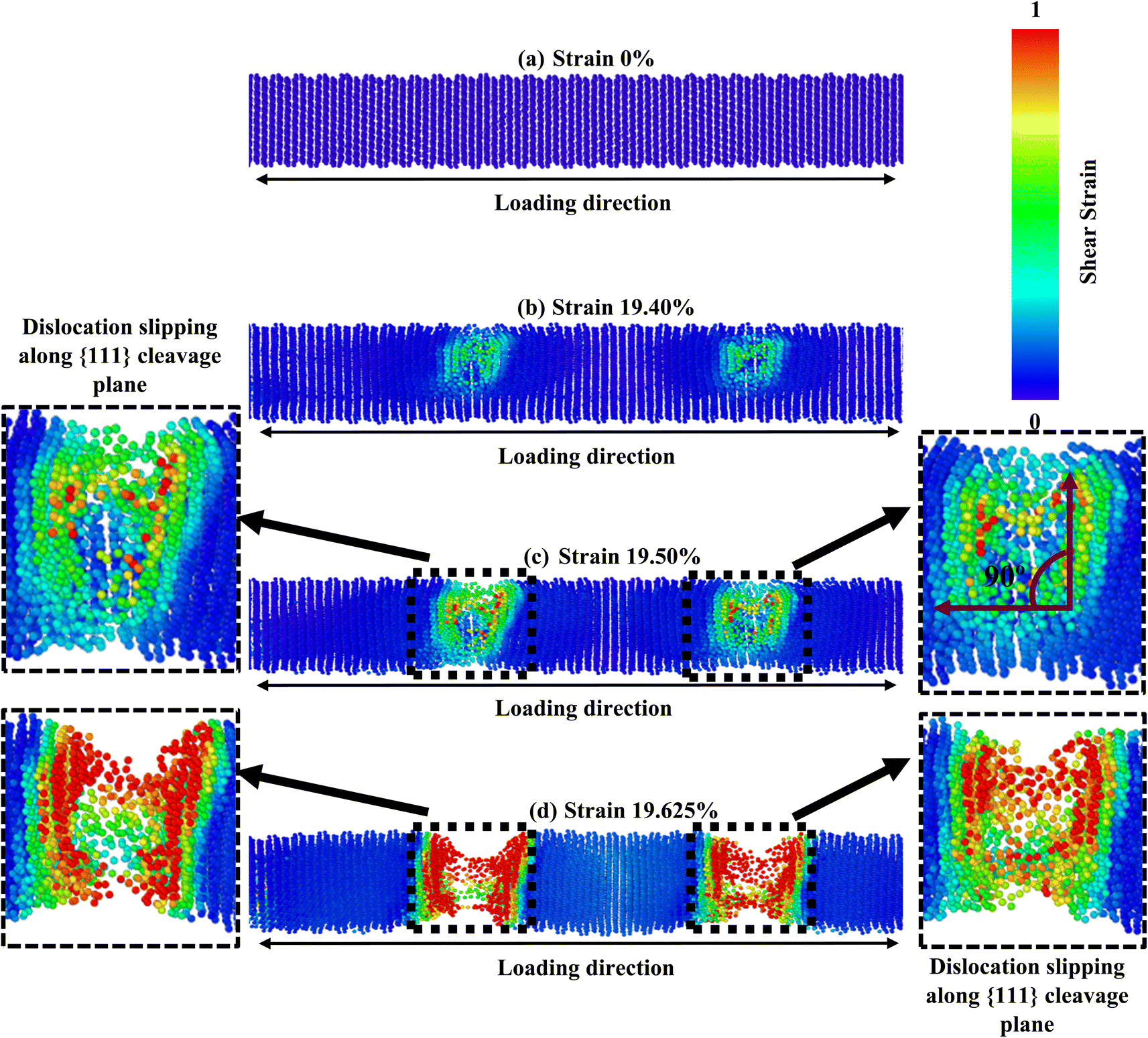 | ||
| Fig. 5 Fracture mechanisms of [111]-oriented 18.25 nm2 ZB ZnTe NW for different strain points at 300 K. The zoomed-in view demonstrates how dislocation slipping caused cleavage along a 90° angle with the applied tension. | ||
However, since the distances among the particles along the [100] orientation are so close (as shown in Fig. 2c), the nucleation of a fracture along the {100} plane would require an enormous extent of energy. A higher tensile strain is required to deform the structure because the bonding exhibits extremely strong rigidity. As seen in Fig. 7, the [100]-oriented NW requires a higher strain value of 20.675% to begin the arrangement's distortion related to other directions because smaller interatomic distances dominate, producing a strong electrostatic attraction force between the planes.38 Additionally, it has been noted that at 300 K or smaller temperatures, the {111} plane can govern the cleavage nucleation when a tensile force is employed in its direction because of its completely activated quality over other planes.30,38,58 As a result of its lesser interplanar gap distance along the [100] orientation, the {100} plane needs to be completely energized. Therefore, the {111} cleavage plane is stimulated with the employed tension, causing results of smaller fracture stress at greater strain. Similar findings have been reported in existing literature pertaining to the mechanical behavior of CdTe and SiGe ZB NWs oriented along the [100] direction.58,64 In addition, the generation and propagation of disorders through fractional slip, full slip, or twinning is the primary source of native deformations that cause ZB NWs to collapse. Under tensile loading, it has been discovered that slip deformation is preferred along the [100] and [111] orientations, whereas twinning is seen in the [110] orientation. Fig. 5 shows that until the strain reaches 19.40%, the [111] ZnTe NW expands elastically. Then, crack initiation occurs across the transverse section in two separate locations, with the cleavage plane {111} vertical to the axial direction [111]. In [110] orientation, the deformation by partial slip/twinning is also preferred along {111} cleavage plane. Furthermore, at room temperature, the NW with [100] axial orientation (Fig. 7) yields a strain of 20.675% after the first elastic stage. The slipping behavior of the [100] NW is comparable to the cleavage of the [111] NW.
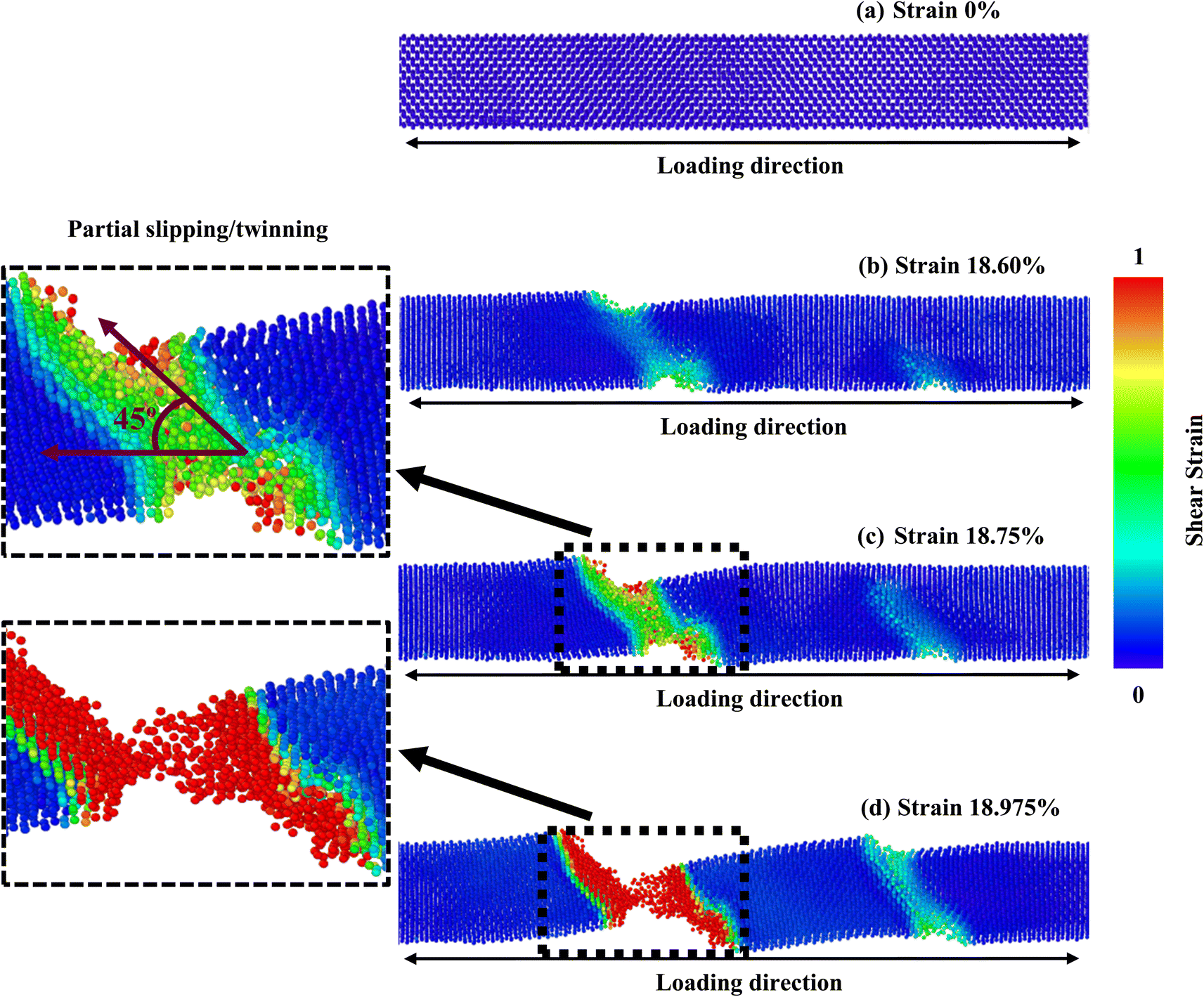 | ||
| Fig. 6 Fracture mechanisms of [110]-oriented 18.25 nm2 ZB ZnTe NW for different strain levels at 300 K. The zoomed-in view demonstrates how partial slipping/twinning caused cleavage at a 45° angle with the applied tension. | ||
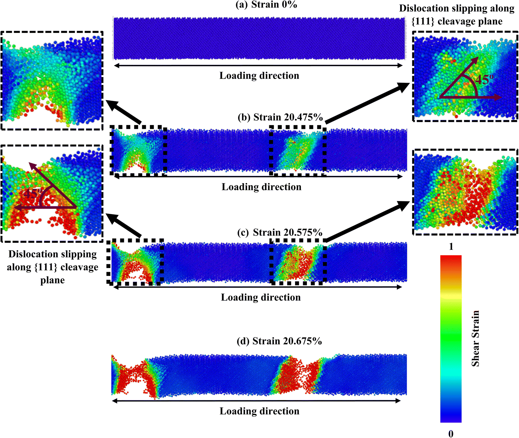 | ||
| Fig. 7 Fracture mechanisms of [100]-oriented 18.25 nm2 ZB ZnTe NW for different strain levels at 300 K. The dislocation slipping-prompted {111} cleavage plane is visible in the zoomed-in view at an angle of 45° with the applied tension. | ||
The [100] crystallographic orientation exhibits the highest percentage decrease in fracture strength as the temperature rises, while the [110] orientation demonstrates the lowest rate of reduction. In contrast, it can be observed that the [111] orientation exhibits the most significant decline in elastic modulus as temperature increases, while the [100] orientation displays the least pronounced decrease. Fig. 8 illustrates the distribution of stress and the arrangement of cracks in a [100]-oriented NW at a temperature of 600 K. It is important to note that we have solely focused on this specific temperature in order to gain a deeper comprehension of the impact of temperature elevation. Fig. 2c–e illustrates that the [111] orientation exhibits the largest interplanar distance when compared to the other two orientations. Therefore, the increased distance between {111} planes facilitate the initiation of cleavage at lower strain levels and across a wider range of temperatures. The initiation of crack propagation in this ZB ZnTe NW is expected to occur along the {111} crystallographic plane. Our study involved examining the deformation mechanism through the application of loads along the [100] orientation. However, our findings indicate that the NW achieves its maximum tensile strength when subjected to a tensile force along the [111] orientation. This does not conflict with the cleavage fracture along the {111} plane under loading in the [100] direction. The fracture of ZnTe NWs initiates along the [100] crystallographic direction when subjected to a strain of 20.475% at a temperature of 300 K. Subsequently, complete failure occurs at a strain of 20.675%. However, when the temperature is increased to 600 K, the structure of ZnTe NWs undergoes deformation at a strain of 19.925%. This phenomenon arises due to the elevated temperatures, which induce increased thermal fluctuations in the atomic bonds of the crystal. Consequently, these thermal disturbances lead to the gradual attenuation of the chemical bonds.30,38
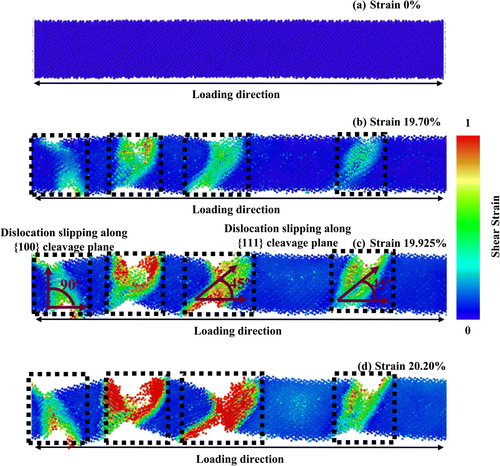 | ||
| Fig. 8 Fracture mechanisms of [100]-oriented 18.25 nm2 ZB ZnTe NW for different strain levels at 600 K. The black dotted structures show the dislocation slipping prompted {100} and {111} cleavage planes along an angle of 90° and 45°, respectively, with the applied tension. | ||
Furthermore, the small strain value is enough to break the bond and create the void at higher temperatures due to the strong thermal trembling effect.30,38 We have also observed that at 300 K, cracks begin to develop at two separate positions of the NWs at 20.475% strain (as shown by the black dashed blocks in Fig. 7), and bonds begin to break at nearly 20.675% strain. This is because, at low temperatures, the structure only encounters a small amount of thermal oscillation. The aforementioned process effectively impedes the propagation of deformation and strain, which would otherwise rapidly propagate from the initial bond break in the NW to the entire structure, including the activation of the {100} plane. At 600 K, nonetheless, the intensity and the frequency of atomic vibration rise, making it easier for atoms to move away from their equilibrium locations. This raises the average distance between atoms and significantly activates the {100} plane. As a result, interplanar distance loses relative significance as the temperature rises. Due to the combined effects of the {111} and {100} cleavage planes, which make an angle of 45° and 90° with the direction of loading, respectively, the crack begins at four different locations (indicated by black square-shaped spotted blocks).30,38 Fig. 7 and 8 show that at 300 K and 600 K temperatures, the {111} plane acts as the principal cleavage plane; hence, with a rising temperature, a greater reduction rate of elastic modulus was found along the [111] orientation. On the other hand, at 300 K, slipping in [100] orientation has occurred due to the cleavage of {111} plane only. However, at 600 K temperature, the {100} cleavage plane also acts as the second principal cleavage plane, and a greater reduction rate of fracture strength with temperature is found along the [100] orientation due to the activation of {111} as well as {100} cleavage planes.
Lastly, the effect of strain rate on the mechanical behavior at 300 K is investigated. Fig. 9 depicts how various strain rates, ranging from 108 s−1 to 1010 s−1, affect the stress–strain behavior of [111], [110], and [100]-oriented ZnTe NWs with a cross-sectional area of about ∼18.25 nm2. It has been found that strain rates do not affect elastic modulus because the stress–strain behavior is independent of them before attaining the maximum stress point.65 However, a reduction in the strain rate reduces the fracture strength and strain. This decrease happens because the atoms have more time to react when the strain rate is slowed, which favors temperature variation and stress liberation. Consequently, the bond dissolves sooner since the atoms can overcome the energy barrier with less strain. At a greater strain rate, however, inadequate time to expand causes fast changes in atoms, causing fractures to nucleate from various areas of the NW simultaneously and spread instantaneously. As a result, minor anomalies in the stress–strain curve are observed at a strain rate of 1010 s−1. Furthermore, as the strain rate rises, fracture strength and strain increase, consistent with earlier findings of similar ZB NWs.30,38,66 It is established that the elastic modulus does not depend on strain rate since the slopes of the stress–strain plots in the elastic region during distortion coincide for various strain rates.
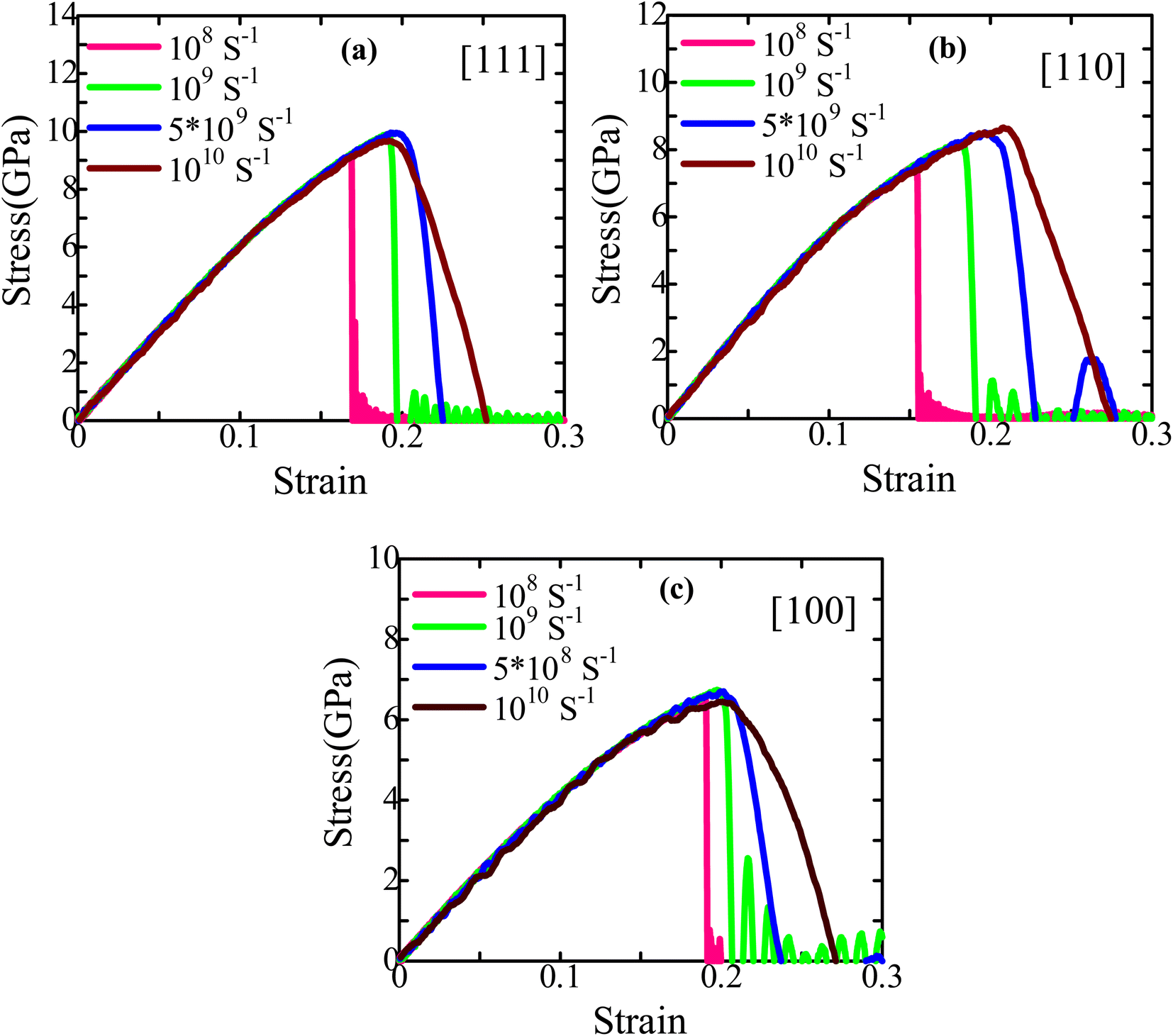 | ||
| Fig. 9 Stress–strain performance curves of (a) [111], (b) [110], and (c) [100]-directed ZB ZnTe NW for dissimilar strain rates at 300 K. | ||
The relation concerning the final fracture strength of ZnTe NW along a specific crystal direction and the strain rate can be comprehended using the Arrhenius equation:67
 | (2) |
![[small epsi, Greek, dot above]](https://www.rsc.org/images/entities/i_char_e0a1.gif) is the strain rate, σ denotes the fracture strength, Q is the activation energy, R defines the universal gas constant, T represents the deformation temperature, m denotes the strain-rate sensitivity, and A is a constant. Considering that the temperature does not change during the duration of the deformation, eqn (2) can be shortened as:
is the strain rate, σ denotes the fracture strength, Q is the activation energy, R defines the universal gas constant, T represents the deformation temperature, m denotes the strain-rate sensitivity, and A is a constant. Considering that the temperature does not change during the duration of the deformation, eqn (2) can be shortened as:
 | (3) |
Subsequently, by exploring the gradients of ln(σ) and ln(), we can use the following equation to find the strain-rate sensitivity factor m along the various growth directions:
 | (4) |
As shown in Fig. 10, the strain-rate sensitivity m for the [111], [110], and [100] orientations are 0.0004, 0.0292, and 0.0132, respectively. Thus, strain rate plays a significant role in the [110] oriented ZB ZnTe NW. The high sensitivity observed in this case may be attributed to the development of deformation mechanisms along the [110] orientation.
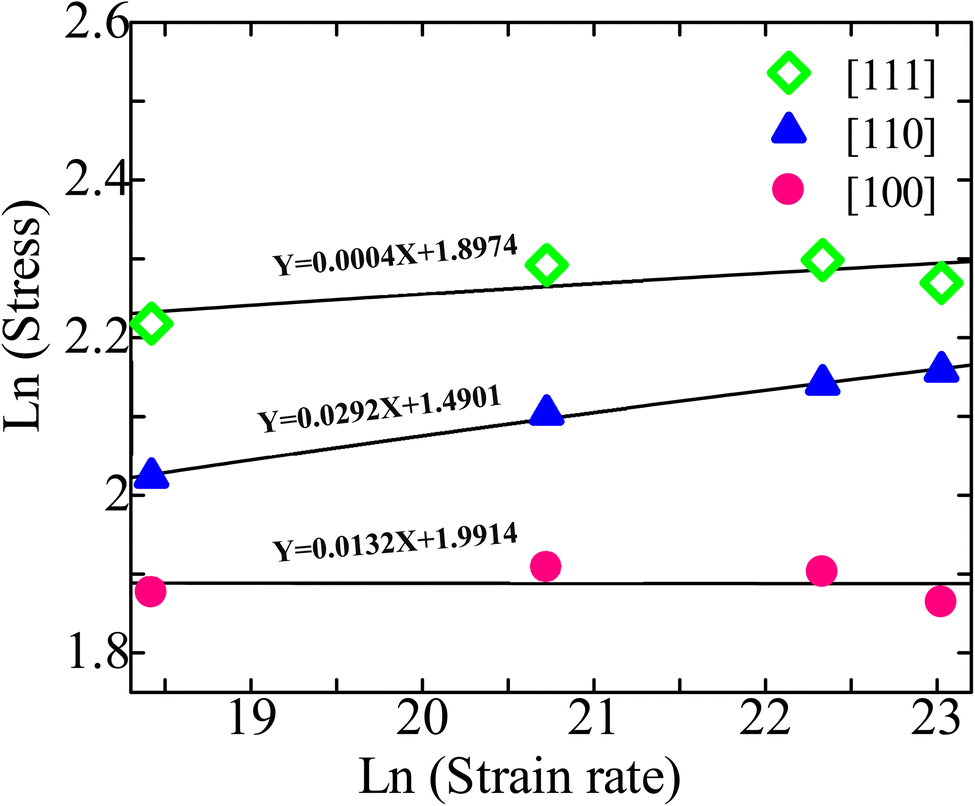 | ||
| Fig. 10 The strain-rate sensitivity of ZB ZnTe NW along three crystal orientations at 300 K. | ||
In this part, we have investigated the PE/atom to understand strain rate sensitivity along various crystal directions. The PE/atom of NW along the [100], [110], and [111] directions are depicted as a function of strain for various strain rates in Fig. S3a–c (ESI†). The PE/atom for various strain rates for all three dissimilar orientations exhibits coincident behavior before attaining the ultimate rupturing stage. As seen in Fig. S3b,† the fracture strain at which the PE/atom curve exhibits a drastically falling nature varies notably for [110]-oriented NW with three diverse strain rates. This fluctuation is much greater than that for the other two directions. Therefore, the [110]-oriented NW has the greatest strain rate sensitivity. We have also investigated the deformation processes of ZnTe NWs along three distinct crystal directions at three dissimilar strain rates to provide qualitative and numeric analyses of strain rate sensitivity. The final stage distortion processes of [100], [110], and [111]-directed NWs are depicted in Fig. 11a–c, respectively, with three distinct strain rates (108 s−1, 109 s−1, and 1010 s−1). These pictures clearly illustrate the variations in deformation patterns for diverse strain rates. From Fig. 11a, it has been noticed that with the rise of strain rates, the number of cracking zones along with different cleavage planes ({111}, {100}) increases significantly for the [100]-oriented ZnTe NWs. No amorphization is noticed in the unaffected zone of this orientation for different strain rates. Similar to the [100] orientation, the [111]-oriented NW exhibits the deformation behavior of an increasing cracking zone along with different cleavage planes with increasing strain rates (shown in Fig. 11c). However, in the case of the [110] orientation (shown in Fig. 11b), we have observed two dislocations slipping in two separate areas of the NW at a strain rate of 108 s−1. At lower strain rates, the dislocation and relaxation processes occur repeatedly. Consequently, the overall crystalline structure transitions from a global state to localized close-packed atomic arrangements. Additionally, the surface of the NW undergoes reconstruction outside the regions experiencing cracking. However, only one fracture zone caused by incomplete twinning was seen in the NW when the strain rate is raised to 109 s−1, which is entirely different from the other two directions. Moreover, an ensemble of various cleavage plane-induced amorphization is noticed when the strain rate is raised to 1010 s−1. Several locations in the NW with cascading relationships are uniformly nucleated through dislocation slipping and deformation twinning. Consequently, the [110]-oriented NW exhibits the formation of crystals with both short-range and long-range order, as well as clustering phenomena. These structural characteristics give rise to notable phase transitions at varying strain rates, thereby inducing a pronounced strain rate sensitivity.
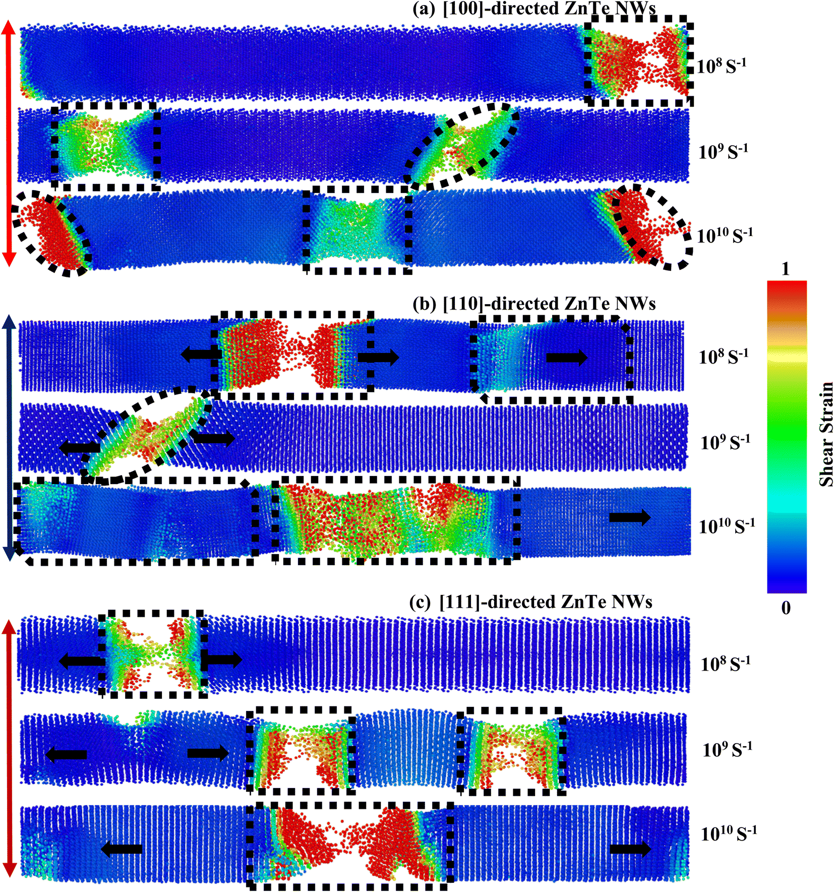 | ||
| Fig. 11 Dissimilarity in the fracture mechanisms of ZB ZnTe NWs for three dissimilar strain rates along the (a) [100], (b) [110], and (c) [111]-orientations. | ||
4. Conclusions
In conclusion, an extensive study of the tensile mechanical performance and deformation mechanisms of ZB ZnTe NWs at the atomic level has been conducted using MD simulations. Diverse orientations, temperatures, and strain rates have been used to study mechanical properties, such as fracture strength, strain, and elastic modulus. We have observed a substantial negative correlation between temperature and the ZB ZnTe NW's fracture strength and elastic modulus. Among the three growth orientations, the [111]-directed NW offers the maximum value of critical strength, elastic modulus, and fracture toughness at all temperatures, while the [100]-oriented NW exhibits the lowest value in all categories. However, the ZnTe NWs exhibit the greatest fracture strain under tensile loading in the [100] direction. Greater fracture stress and strain have been exposed at a higher strain rate. Most importantly, it is found that the [110]-directed ZnTe NW has the greatest strain rate sensitivity among three different configurations. At ambient temperature and in all directions, it is noted that the {111} planes are the primary cleavage planes; however, when the temperature is raised, the {100} plane is activated and acts as the additional primary cleavage plane. It has been noticed that with the increase in strain rates, the number of cracking zones along with different cleavage planes ({111}, {100}) increases significantly for both the [100] and [111]-oriented NWs. No amorphization is noticed in the unaffected zone for both [100] and [111] orientations at different strain rates. However, the [110]-oriented NW exhibits the formation of crystals with both short-range and long-range order as well as clustering phenomena, leading to significant structural phase transitions and producing strong strain rate sensitivity. This work would be very helpful in different eras of nanoelectronics, NEMS, and optoelectronics systems where NW deformation is urgently needed to produce system output.Data availability
All data generated or analyzed during this study are included in this manuscript and its ESI† file.Author contributions
A. S. M. Jannatul Islam: conceptualization, methodology, software, investigation, writing – original draft. Md. Sherajul Islam: visualization, investigation, supervision, writing – review & editing. Md. Sayed Hasan: software, investigation, writing – original draft. Kamal Hosen: writing – review & editing. Md. Shahadat Akbar: software and data curation. A. G. Bhuiyan and Jeongwon Park: supervision, writing – review & editing.Conflicts of interest
There are no conflicts of interest to declare.Acknowledgements
This study was supported by the facilities of the UGC-funded research project (grant no. CASR-59/24, 2021–2022) provided by the CASR at Khulna University of Engineering & Technology, Bangladesh.References
- P. C. McIntyre and A. Fontcuberta i Morral, Mater. Today Nano, 2020, 9, 100058 CrossRef.
- H. S. Jang, T. H. Kim, B. G. Kim, B. Hou, I. H. Lee, S. H. Jung, J. H. Lee, S. Cha, C. W. Yang, B. S. Kim and D. Whang, Nano Lett., 2021, 21, 9909–9915 CrossRef CAS.
- M. Nehra, N. Dilbaghi, G. Marrazza, A. Kaushik, R. Abolhassani, Y. K. Mishra, K. H. Kim and S. Kumar, Nano Energy, 2020, 76, 104991 CrossRef CAS.
- J. Kosmaca, R. Meija, M. Antsov, G. Kunakova, R. Sondors, I. Iatsunskyi, E. Coy, J. Doherty, S. Biswas, J. D. Holmes and D. Erts, Nanoscale, 2019, 11, 13612–13619 RSC.
- B. Zheng and J. E. Lowther, Nanoscale, 2010, 2, 1733–1739 RSC.
- X. Wang, J. Song and Z. L. Wang, J. Mater. Chem., 2007, 17, 711–720 RSC.
- J. Jie, W. Zhang, I. Bello, C. S. Lee and S. T. Lee, Nano Today, 2010, 5, 313–336 CrossRef CAS.
- T. Mandal, P. K. Maiti and C. Dasgupta, Phys. Rev. B: Condens. Matter Mater. Phys., 2012, 86, 024101 CrossRef.
- Z. Wang, X. Zu, L. Yang, F. Gao and W. J. Weber, Phys. Rev. B: Condens. Matter Mater. Phys., 2007, 76, 045310 CrossRef.
- X. R. Zhuo and H. G. Beom, Comput. Mater. Sci., 2018, 152, 331–336 CrossRef CAS.
- A. S. M. J. Islam, M. S. Hasan, M. S. Islam, A. G. Bhuiyan, C. Stampfl and J. Park, Sci. Rep., 2023, 13, 1–17 CrossRef PubMed.
- R. Tao, G. Ardila, L. Montès and M. Mouis, Nano Energy, 2015, 14, 62–76 CrossRef CAS.
- B. Tekcan, B. van Kasteren, S. V. Grayli, D. Shen, M. C. Tam, D. Ban, Z. Wasilewski, A. W. Tsen and M. E. Reimer, Sci. Rep., 2022, 12, 1–8 CrossRef PubMed.
- Q. Mahmood, G. Murtaza, G. Ali, M. Hassan, E. Algrafy, M. S. Shahid, N. A. Kattan and A. Laref, J. Alloys Compd., 2020, 834, 155176 CrossRef CAS.
- A. Artioli, P. Rueda-Fonseca, P. Stepanov, E. Bellet-Amalric, M. Den Hertog, C. Bougerol, Y. Genuist, F. Donatini, R. André, G. Nogues, K. Kheng, S. Tatarenko, D. Ferrand and J. Cibert, Appl. Phys. Lett., 2013, 103, 222106 CrossRef.
- B. B. Wang, M. K. Zhu, H. Wang and G. B. Dong, Opt. Mater., 2011, 34, 42–47 CrossRef CAS.
- A. S. M. J. Islam, M. S. Islam, N. Ferdous, J. Park, A. G. Bhuiyan and A. Hashimoto, Nanotechnology, 2019, 30, 445707 CrossRef CAS.
- A. S. M. J. Islam, M. S. Islam, M. R. Islam, C. Stampfl and J. Park, Nanotechnology, 2021, 32, 435703 CrossRef CAS.
- P. Rueda-Fonseca, E. Bellet-Amalric, R. Vigliaturo, M. Den Hertog, Y. Genuist, R. André, E. Robin, A. Artioli, P. Stepanov, D. Ferrand, K. Kheng, S. Tatarenko and J. Cibert, Nano Lett., 2014, 14, 1877–1883 CrossRef CAS.
- F. Boutaiba, A. Belabbes, M. Ferhat and F. Bechstedt, Phys. Rev. B: Condens. Matter Mater. Phys., 2014, 89, 245308 CrossRef.
- P. Harder, A. Nielsen, A. K. Sassnau, D. Bonatz, M. Perbandt, T. Kipp and A. Mews, Chem. Mater., 2021, 33, 1061–1069 CrossRef CAS.
- R. A. Bernal, R. Agrawal, B. Peng, K. A. Bertness, N. A. Sanford, A. V. Davydov and H. D. Espinosa, Nano Lett., 2011, 11, 548–555 CrossRef CAS.
- T. Kuykendall, P. J. Pauzauskie, Y. Zhang, J. Goldberger, D. Sirbuly, J. Denlinger and P. Yang, Nat. Mater., 2004, 3, 524–528 CrossRef CAS.
- W. Li, X. Cui, R. Zeng, G. Du, Z. Sun, R. Zheng, S. P. Ringer and S. X. Dou, Sci. Rep., 2015, 5, 1–8 Search PubMed.
- X. R. Zhuo and H. G. Beom, Cryst., 2019, 9, 102 CrossRef CAS.
- C. Ji and H. S. Park, Nanotechnology, 2007, 18, 305704 CrossRef.
- Z. Yang, L. Zheng, Y. Yue and Z. Lu, Sci. Rep., 2017, 1–9 Search PubMed.
- Q. Liu and S. Shen, Int. J. Plast., 2012, 38, 146–158 CrossRef CAS.
- K. L. Firestein, D. G. Kvashnin, J. F. S. Fernando, C. Zhang, D. P. Siriwardena, P. B. Sorokin and D. V. Golberg, Nano Lett., 2019, 19, 2084–2091 CrossRef CAS PubMed.
- E. H. Chowdhury, M. H. Rahman, R. Jayan and M. M. Islam, Comput. Mater. Sci., 2021, 186, 110001 CrossRef CAS.
- C. Dong, X. Lu, P. Yang, X. Guo, J. Ren, H. Xue, J. Li, F. Tang, H. Li, Y. Ding and P. La, J. Alloys Compd., 2021, 870, 159476 CrossRef CAS.
- H. Cao, W. Chen, Z. Rui and C. Yan, Nanotechnology, 2022, 33, 365702 CrossRef.
- L. Chang, C. Y. Zhou, H. X. Liu, J. Li and X. H. He, J. Mater. Sci. Technol., 2018, 34, 864–877 CrossRef.
- D. Wang, J. Zhao, S. Hu, X. Yin, S. Liang, Y. Liu and S. Deng, Nano Lett., 2007, 7, 1208–1212 CrossRef CAS.
- D. T. Ho, Y. Im, S. Y. Kwon, Y. Y. Earmme and S. Y. Kim, Sci. Rep., 2015, 5, 11050 CrossRef CAS.
- R. Khenata, A. Bouhemadou, M. Sahnoun, A. H. Reshak, H. Baltache and M. Rabah, Comput. Mater. Sci., 2006, 38, 29–38 CrossRef CAS.
- J. Schrier, D. O. Demchenko, L. W. Wang and A. P. Alivisatos, Nano Lett., 2007, 7, 2377–2382 CrossRef CAS PubMed.
- T. H. Pial, T. Rakib, S. Mojumder, M. Motalab and M. A. S. Akanda, Phys. Chem. Chem. Phys., 2018, 20, 8647–8657 RSC.
- X. W. Zhou, D. K. Ward, J. E. Martin, F. B. Van Swol, J. L. Cruz-Campa and D. Zubia, Phys. Rev. B: Condens. Matter Mater. Phys., 2013, 88, 085309 CrossRef.
- P. Hirel, Comput. Phys. Commun., 2015, 197, 212–219 CrossRef CAS.
- D. H. Tsai, J. Chem. Phys., 1979, 70, 1375–1382 CrossRef CAS.
- C. Soykan, S. O. Kart and T. Cagın, Arch. Mater. Sci. Eng., 2010, 116, 115–119 Search PubMed.
- S. Plimpton, J. Comput. Phys., 1995, 117, 1–19 CrossRef CAS.
- A. Stukowski, Modell. Simul. Mater. Sci. Eng., 2010, 18, 015012 CrossRef.
- A. S. M. J. Islam, M. S. Islam, N. Ferdous, J. Park and A. Hashimoto, Phys. Chem. Chem. Phys., 2020, 22, 13592–13602 RSC.
- G. Zou, H. Li, Y. Zhang, K. Xiong and Y. Qian, Nanotechnology, 2006, 17, S313 CrossRef CAS.
- A. M. Morales and C. M. Lieber, Science, 1998, 279, 208–211 CrossRef CAS PubMed.
- N. Wang, Y. Cai and R. Q. Zhang, Mater. Sci. Eng., R, 2008, 60, 1–51 CrossRef.
- G. Sainath and B. K. Choudhary, Comput. Mater. Sci., 2016, 111, 406–415 CrossRef CAS.
- Q. Meng, C. Jiang and S. X. Mao, J. Cryst. Growth, 2008, 310, 4481–4486 CrossRef CAS.
- E. Janik, J. Sadowski, P. Dłuzdotewski, S. Kret, L. T. Baczewski, A. Petroutchik, E. ŁUsakowska, J. Wróbel, W. Zaleszczyk, G. Karczewski, T. Wojtowicz and A. Presz, Appl. Phys. Lett., 2006, 89(13), 133114 CrossRef.
- X. Yan, Y. Liu, C. Zha, X. Zhang, Y. Zhang and X. Ren, Nanoscale, 2023, 15, 3032–3050 RSC.
- K. Zhang, Y. Abbas, S. U. Jan, L. Gao, Y. Ma, Z. Mi, X. Liu, Y. Xuan and J. R. Gong, ACS Appl. Mater. Interfaces, 2020, 12, 17676–17685 CrossRef CAS.
- H. A. Fonseka, P. Caroff, J. Wong-Leung, A. S. Ameruddin, H. H. Tan and C. Jagadish, ACS Nano, 2014, 8, 6945–6954 CrossRef CAS PubMed.
- E. Janik, P. Dłuzewski, S. Kret, A. Presz, H. Kirmse, W. Neumann, W. Zaleszczyk, L. T. Baczewski, A. Petroutchik, E. Dynowska, J. Sadowski, W. Caliebe, G. Karczewski and T. Wojtowicz, Nanotechnology, 2007, 18, 475606 CrossRef.
- E. Dynowska, W. Szuszkiewicz, J. Z. Domagala, E. Janik, A. Presz, T. Wojtowicz, G. Karczewski and W. Caliebe, Radiat. Phys. Chem., 2009, 78, S120–S124 CrossRef CAS.
- X. Li, J. Ni and R. Zhang, Sci. Rep., 2017, 7, 1–8 CrossRef PubMed.
- M. A. M. Munshi, S. Majumder, M. Motalab and S. Saha, Mater. Res. Express, 2019, 6, 105083 CrossRef CAS.
- M. B. Kanoun, A. E. Merad, H. Aourag, J. Cibert and G. Merad, Solid State Sci., 2003, 5, 1211–1216 CrossRef CAS.
- B. H. Lee, J. Appl. Phys., 2003, 41, 2988 CrossRef.
- A. S. M. J. Islam, M. S. Islam, N. Z. Mim, M. S. Akbar, M. S. Hasan, M. R. Islam, C. Stampfl and J. Park, ACS Omega, 2022, 7, 4525–4537 CrossRef CAS PubMed.
- A. S. M. J. Islam, M. S. Islam, M. S. Hasan, M. S. Akbar and J. Park, ACS Omega, 2022, 7, 14678–14689 CrossRef CAS PubMed.
- A. S. M. J. Islam, M. S. Akbar, M. S. Islam and J. Park, ACS Omega, 2021, 6, 21861–21871 CrossRef CAS PubMed.
- M. H. Rahman, E. H. Chowdhury and M. M. Islam, J. Nanopart. Res., 2020, 22, 1–12 CrossRef.
- A. S. M. J. Islam, M. S. Islam, N. Ferdous, J. Park, A. G. Bhuiyan and A. Hashimoto, Mater. Res. Express, 2019, 6, 125073 CrossRef CAS.
- H. Tsuzuki, J. P. Rino and P. S. Branicio, J. Phys. D: Appl. Phys., 2011, 44, 055405 CrossRef.
- A. S. M. J. Islam, M. S. Hasan, M. S. Islam and J. Park, Comput. Mater. Sci., 2021, 200, 110824 CrossRef CAS.
Footnote |
| † Electronic supplementary information (ESI) available. See DOI: https://doi.org/10.1039/d3ra03825d |
| This journal is © The Royal Society of Chemistry 2023 |