
 Open Access Article
 This Open Access Article is licensed under a Creative Commons Attribution-Non Commercial 3.0 Unported Licence
Annealing-induced phase transformation in In10Se70Te20 thin films and its structural, optical and morphological changes for optoelectronic applications†
Sasmita Giria,
P. Priyadarshinia,
D. Alagarasanbc,
R. Ganesanc and
R. Naik *a
*a
aDepartment of Engineering and Material Physics, ICT-IOC, Bhubaneswar, 751013, India. E-mail: ramakanta.naik@gmail.com
bNitte Meenakshi Institute of Technology, Yelahanka, Bengaluru, 560064, India
cDepartment of Physics, Indian Institute of Science, Bangalore, 560012, India
First published on 22nd August 2023
Abstract
In2Se3 and In2Te3 have great importance in various device fabrications. The present report is based on the annealing-induced phase formation of both In2Se3 and In2Te3 from In10Se70Te20 thin films at different annealing temperatures as found from the XRD analysis and well supported by the Raman study. The average crystallite size increased with a decrease in the dislocation density. The surface morphology changed with annealing and increased in particle size as noticed from the FESEM images. The uniform distribution and presence of constituent elements in the film were verified using EDX data. The increase in transmittance is accompanied by a decrease in extinction coefficient, optical density and increase in skin depth with annealing. The increase in optical bandgap from 0.418 eV to 0.645 eV upon annealing at 250 °C is associated with a decrease in disorder. The steepness parameter increased and the Se–p value decreased with annealing. The refractive index decreased with an increase in oscillator energy and decrease in dispersion energy. The quality factor, dielectric loss, optical conductivity and electrical susceptibility decreased. The optical electronegativity and plasma frequency increased with annealing. There is a significant change in the non-linear susceptibility and non-linear refractive index with annealing. The observed changes in the film structure and optical behaviour are due to the annealing-induced phase formation from the In10Se70Te20 host matrix upon annealing. Such materials are suitable for optoelectronic and phase change devices.
1. Introduction
The large transparency window in IR regions by Te- and Se-doped chalcogenide films is important owing to their applications in phase change memory devices, photodetectors, photovoltaics, solar cells, infrared detectors, etc.1–5 Se-based materials are used for imaging and biomedical applications, whereas Te-based materials are used for infrared detectors and phase-change memory devices.6 Se-based chalcogenide compounds possess high transmission ability in the mid and far IR range and possess strong non-linearity.7 Se-based materials have advantages such as low melting point, low thermal conductivity, and stability, and they possess the property of easy formation of compounds with doping elements.8,9 Similarly, Te has unique properties for cutting-edge technologies with chalcogenides.10 The high transmittance in the far infra-red regime is used for IR optics and optical fibers.11,12 The ultrafast crystallization of Te-based materials is used in phase change optical data storage devices.13–16 Binary compounds based on Te–Se alloys have been studied widely because they have fast access to information, great storage capacity, and electro photographic applications, such as laser printing and photoreceptors in photocopying.17,18 Se–Te binary compounds have more advantages than pure Se because of their greater hardness, high photosensitivity, higher crystallization temperature, and low aging effects. The thin film forms of Se–Te compounds are promising owing to their wide applications.19 Se–Te alloys are prime candidates for thermoelectric power, and many semiconducting chalcogenide compounds have been reported for the direct energy conversion of thermal to electrical energy.20,21 Thermally evaporated SexTe1−x thin films with tuneable energy gaps are used for high-performance SWIR photodetector fabrication.2 The additive of metallic components to the Se–Te matrix has led to high thermal stability.17 The introduction of In into either Te or Se is very attractive for various applications.In2Te3 is a layer III–IV type material that is sensitive to strain and pressure and is used for superconductor applications.22 The α-In2Te3 films have stable photo switching ability ranging from 370–1064 nm with a short response time of 15 ms. The good figure-of-merit, stability and broad spectral range of α-In2Te3 are used for next-generation photo detectors.23 In2Te3 is having a direct band gap of ∼1.1 eV with a high absorption coefficient value of over 500–2500 nm, which makes it a suitable absorber layer in photovoltaic cells.24,25
Similarly, In2Se3 has shown attractive properties and great potential in the applications of ferroelectric devices.26 The leveraging of the semiconducting and ferroelectricity nature of α-In2Se3 and ferroelectric semiconductor field-effect transistors (FeSFETs) are made for neuromorphic instruments for brain-inspired intelligent systems.27 The β-In2Se3 nanosheets are a type of indirect band gap semiconductors with Eg of ∼1.55 eV. Single nanosheet photodetectors possess fast response times and high photoresponsivity.28 The facile integration, patterning, and packaging of high-quality 2D chalcogenide In2Se3 are used for wearable electronics, next-generation photodetector arrays, and integrated optoelectronic circuits.29 However, ternary compounds with In–Se–Te are of great importance in research.
In–Se–Te-based ternary alloys have various structural changes, such as β and α phases, and vacant of In sub-lattices for one-third or two-third for other dopant impurities. Therefore, the appearance of the In–Se and In–Te phases from the phase diagram infers the formation of In2Se3 and In2Te3 phases. Among them, indium-doped Se–Te alloys have found great importance in various devices because of their enhanced optical properties.30 Elkatlawy et al. prepared Se80Te20−xInx thin films with different compositions and revealed that In doping Se80Te20−xInx improved the transmittance range and refractive index in visible and near IR regions.31 Saxena et al. reported an increase in thermal conductivity and thermal diffusivity in Se80Te20−xInx bulk with indium addition.32 Se–Te–In ternary compounds have wide applications in photoreceptors, optical recording media, xerography, infrared spectroscopy, and laser fiber techniques.33,34 Such ternary compounds under different energy treatments, such as laser irradiation, ion irradiation, thermal annealing, proton and irradiation, show profound property modifications, which are useful for many applications.35–38
The In2Se3 band gap is found to be reduced by annealing for the increase in the width of localized states near the band edges. The change in film density reduced the transmittance and increased the absorption, making it suitable for solar cell applications.39 The reduction in the band gap in Se75−xTe25Inx with annealing is a good one because of the material to be used in optical storage.40 Thermal annealing on Se80Te20−xInx thin films changed the structure from amorphous to crystalline with annealing temperature and an increase in refractive index with a reduction in bandgap with annealing time duration.41 By considering the importance of thermal annealing, this study is based on the thermal annealing of In10Se70Te20 thin films at various temperatures.
The prime objective of the study is to observe (i) the thermal annealing-induced structural changes in In10Se70Te20 thin films at various annealing temperatures, (ii) the change in linear-nonlinear optical properties and (iii) morphological changes due to phase transformation in the films. The prepared film samples were thermally annealed at the following temperatures: 100, 150, 200, and 250 °C. X-ray diffraction (XRD) confirms the structural properties, which are strongly corroborated by performing Raman analysis. Field emission scanning electron microscopy (FESEM) was used for the surface morphology imaging. The composition of the films was confirmed by energy dispersive X-ray analysis (EDX). The optical parameters of the annealed In10Se70Te20 thin films were analysed using UV-Visible spectroscopy.
2. Experimental
2.1. Thin film preparation
The bulk In10Se70Te20 samples were prepared using high pure In, Se, Te (Sigma Aldrich, 99.999%) elements by applying the melt quenching method. The required chemical amounts were sealed at a vacuum of 10−5 Torr inside the quartz ampoule and placed inside a furnace at 500 °C for 30 h. The melt formed inside the ampoule was quenched rapidly in liquid nitrogen to obtain the bulk In10Se70Te20 sample. From the prepared bulk sample, In10Se70Te20 thin films were deposited by employing the thermal evaporation method using an HHV (Smart Coat 3) vacuum coating unit.About 800 nm thickness of In10Se70Te20 thin films was deposited on clean substrates (corning glass) at a rate of 5 Å per second. During the whole deposition process, the pressure inside the deposition chamber was maintained at ∼5 × 10⁻⁵ Torr, and the substrate temperature was kept at room temperature. The substrate holder was rotated slowly to obtain a homogeneous and uniform film. The film thickness was controlled by the filament current using the current-controlling unit. A crystal sensor is fixed in the deposition chamber to measure the film thickness, which is recorded and displayed on the digital thickness monitor. The thin films were annealed for 1.5 hours at 100, 150, 200, and 250 °C in a hot air oven.
2.2. Characterization
The structural properties were studied using a Bruker D8 Advance XRD unit with Cu Kα-radiation of wavelength λ = 1.5418 Å. The XRD data were recorded with a step size of 0.02° s−1 for the range from 2θ = 10° to 70°. The change in vibrational mode was determined from Raman spectroscopy (LabRAM HR system) using a 532 nm argon laser source with a CCD detector in backscattering mode. The spectra were recorded from the 50–400 cm−1 range. The spectra calibration was done using the silicon 520 cm−1 line, and 3–4 measurements were taken after calibration at different positions for the same time intervals (40 seconds) to minimize the systematic error. Furthermore, the morphology was imaged using an FESEM (JEOL-JSM-7610F) unit, and the ratio of elemental composition was observed from the EDX unit attached to the FESEM unit. The imaging was done at a voltage of 20 kV during the characterization process.The transmittance and absorbance spectra of as-prepared and annealed In10Se70Te20 thin films were recorded from the JASCO V-770 UV-Visible spectrophotometer in the wavelength range of 500–2500 nm. The linear and non-linear optical properties were calculated from the transmission data using various relations.
3. Results and discussion
3.1. Structural study by XRD and Raman spectroscopy
The XRD pattern of In10Se70Te20 (as-prepared and annealed) thin films is shown in Fig. 1a, which confirms the crystalline nature with the appearance of In2Te3, In4Se3, and In4Te3 phases in the films. The as-prepared film showed crystalline peaks at 23.95° (5 1 1) and 41.13° (8 2 2), corresponding to the cubic phase of In2Te3 phase (ICSD: 33-1488) and a peak at 29.46° (0 4 0) representing the orthorhombic In4Se3 phase (ICDS: 48-1575). Among these three crystalline peaks, the former two peaks remain intact with intensity and position. However, the peak intensity of the In4Se3 peak becomes more intense and prominent with annealing, which is possibly due to thermal energy through annealing. Furthermore, annealing of the In10Se70Te20 thin films results in the appearance of additional peaks at 23.41° (0 1 1) and 48.56° (8 0 0), corresponding to the same orthorhombic In4Se3 phase (ICDS: 48-1575). The crystalline peaks at 28.76° (3 1 1), 44.65° (3 5 1), and 51.11° (7 3 1) present the orthorhombic In4Te3 phase (ICDS: 01-071-2085), respectively. It is noteworthy that the intensity, peak number, and sharpness of the peaks are enhanced with annealing, which ensures increased crystallinity through the formation of large crystallites, as confirmed by several studies.42,43 The formation of more binary In-chalcogen phases might be due to the sufficient kinetic energy of indium, which allows more diffusion of indium with chalcogen lattices (here selenium and tellurium), with annealing temperature and forms bonds with Se and Te atoms.44 In other words, the defects and unsaturated bonds are annealed out by forming many saturated bonds at boundaries with an increased annealing temperature. Such bonds cause structural variation in annealed In10Se70Te20 films. | ||
| Fig. 1 (a) XRD pattern and (b) Raman spectra of In10Se70Te20 thin films. | ||
Based on the XRD pattern, the average crystallite size (D) calculated from the full-width half maxima (FWHM) observed prominent peaks using Scherer's equation:45
 | (1) |
 | (2) |
 | (3) |
| Structural parameters | D (nm) | δ ×1015 (m−2) | ε | NC (nm−2) |
|---|---|---|---|---|
| As-prepared | 9.55 | 0.0109 | 0.014 | 0.91 |
| Annl 100 °C | 12.90 | 0.0060 | 0.011 | 0.37 |
| Annl 150 °C | 13.17 | 0.0057 | 0.010 | 0.35 |
| Annl 200 °C | 14.43 | 0.0047 | 0.008 | 0.26 |
| Annl 250 °C | 18.68 | 0.0028 | 0.005 | 0.12 |
Raman spectroscopic analysis is an effective method for studying the structural aspects of non-crystalline compounds. The nature of the chemical bonds, atomic arrangements, and structural changes in vibrational levels induced by external energy were viewed through Raman analysis. The Raman data of In10Se70Te20 thin film are presented in Fig. 1b, which depicts different peaks ranging from 50 to 600 cm−1 for the as-prepared and annealed films. The as-deposited In10Se70Te10 thin film has peaks at 95, 151, and 190 cm−1, corresponding to the In–Se phase.49–51 Annealing led to the appearance of extra peaks at 127, 172 and 249 cm−1 with variation in intensity. The peak at 127 cm−1 is related to the γ-In2Se3 phase.51 The latter two Raman peaks were attributed to the Te–Te52 bond vibration and Sen rings.50,53 The intensity increase in the Raman peaks and low shift towards higher wavenumbers with annealing might be due to annealing-induced structural changes inside the matrix.
3.2. Morphology study using FESEM and EDX
For imaging the microstructure and morphology study of any material, FESEM is one of the most important tools. The morphological structure of the In10Se70Te20 (as-prepared and annealed) thin films was analysed by FESEM images, as shown in Fig. 2. The morphological images at a scale of 200 nm illustrate the uniformity of the films. The annealing-induced morphological changes were clearly observed in the granular structure of the annealed films. The particle size was calculated using ImageJ software (version-Java 1.8.0_172), with statistical analysis, as presented in Fig. 3. With an increased annealing temperature, the average particle size increased, as demonstrated in Fig. 3.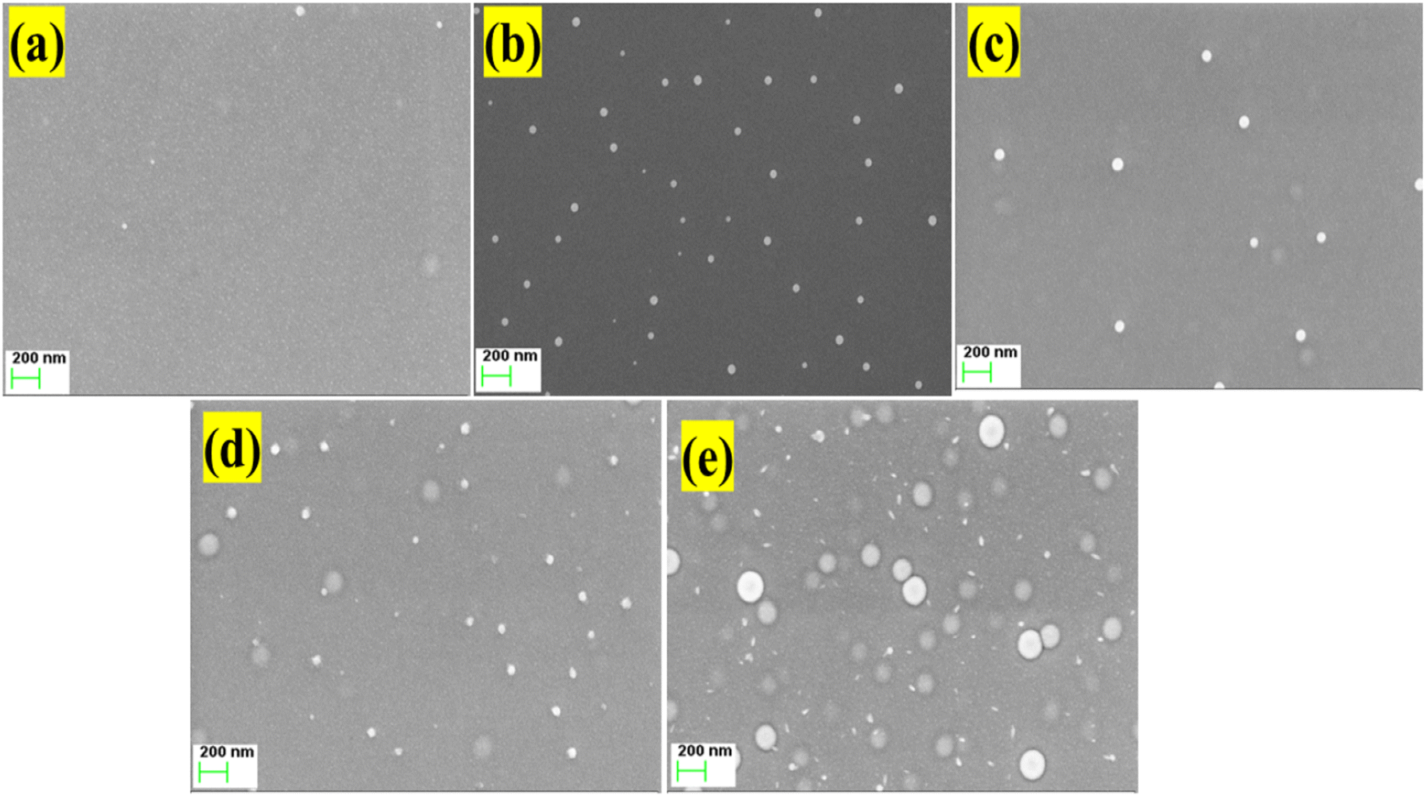 | ||
| Fig. 2 FESEM images for surface morphological analysis of In10Se70Te20 thin films. | ||
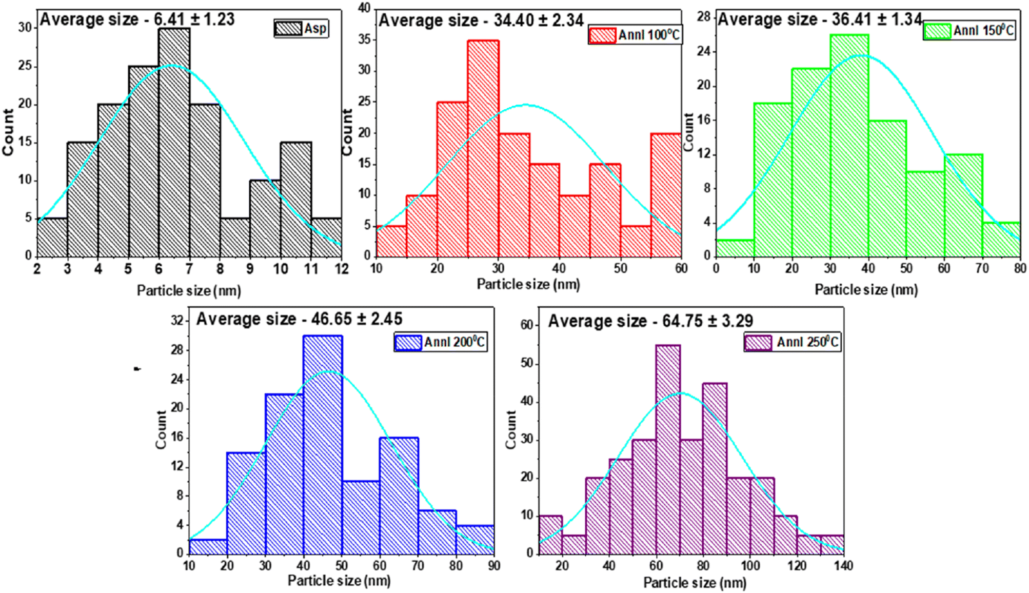 | ||
| Fig. 3 Particle size distribution of the In10Se70Te20 thin films. | ||
Elemental analysis was performed using EDX, which showed the presence of In, Te, and Se components (Fig. 4) in the annealed and as-prepared films. The distinct peaks refer to the relevant components, and the composition of the various samples is closely the same within a 2% error of the estimated one. The uniform distribution of constituent elements through elemental mapping obtained from EDX for the as-deposited In10Se70Te20 film is shown in Fig. 5, and the 250 °C annealed film is shown in ESI Fig. S1.†
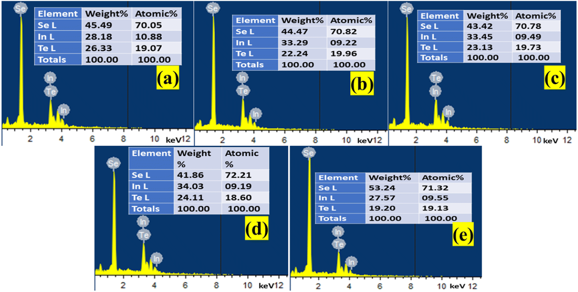 | ||
| Fig. 4 EDX spectra for compositional analysis of In10Se70Te20 thin films. | ||
 | ||
| Fig. 5 EDX mapping of the elements in the as-prepared In10Se70Te20 film. | ||
3.3. Optical property study
 | ||
| Fig. 6 Change in (a) transmittance, (b) extinction coefficient with wavelength, (c) optical density and (d) skin depth with energy of In10Se70Te20 thin films. | ||
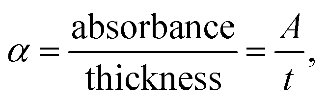
The optical absorbance provides valuable information related to the bandgap and band structure of both crystalline and amorphous materials. There is a shift in the absorption edge to the lower wavelength side, which is due to the thermal bleaching effect, thus inferring an increase in bandgap energy with annealing.58 The optical absorption edge appears because of the electronic transition in the semiconductor.58,59 Here, the absorption edge region lies in the range of 750–1200 nm, and the coefficient (α) was determined from the absorbance value using the following equation:
 | (4) |
Thermal annealing at and above Tg minimizes the structural imperfections, resulting in few available states for photon absorption within the band gap. The local structure in the film changes because of the bond breaking and rearrangements due to annealing. This results in a shift in the absorption edge and substantial reconfiguration at the atomic and molecular levels, ultimately changing the optical parameters of the film.61
The extinction coefficient (k) represents the polarization ability of the material, which is dependent on ‘α’ using the following formula:56 k = (αλ/4π). The ‘k’ infers the interaction between the electric field of the incident waves and the film. The ‘k’ value decreased with wavelength, as shown in Fig. 6b for the annealed and as-deposited one. This behaviour is owing to the decrease in ‘α’ with an increase in ‘λ’. The heat treatment annealed out the unsaturated defects and produced a large number of saturated bonds after annealing. The density of the localized state change because annealing modifies the ‘k’ value.62 The as-prepared In10Se70Te20 sample showed crystallinity with the appearance of In2Te3 and In4Se3 phases. The increase in the annealing temperature led to an increase in crystallinity. This might be due to the annealing process that provides sufficient energy to the atoms, enabling them to migrate from their relative equilibrium position. Consequently, grain growth increases, and lattice dislocation decreases. This causes an increase in lattice perfection and lattice growth.63,64 This causes changes in the optical properties by improving the transmittance and shifting the absorption edges. The blue shifting in the absorption edge reduced the absorption coefficient, representing light absorption through the material medium. The extinction coefficient, refractive index, and non-linear parameters are all related to the absorption coefficient. Therefore, these parameters showed a reducing pattern with annealing temperature.
The absorption capability of the film is also represented by another optical quantity so called optical density (OD). It signifies the degree to which a refractive medium retards transmitted light rays. Fig. 6c depicts the change in OD (= α × t, where ‘t’ is the film thickness and ‘α’ is the absorption coefficient), which decreased with an increase in annealing temperature. In thin films, OD is due to the refraction and scattering of light, measuring the velocity of light in the material.65 The absorbance is very low (below 2%) at a lower hν, which leads to an enhancement in the transmittance of electromagnetic waves in a low absorbance regime. This behavior is responsible for the high IR transmission in In–Se–Te chalcogenide thin films. The decrease in OD value accounts for the increase in the velocity of light inside the material with annealing. The material concentration decreased, resulting in an increase in optical transparency as obtained in the transmission spectra.
The penetration depth, so-called skin depth (δ), is measured as the length scale at which the absorbance of incident photon becomes 1/e of its value inside the film surface. The value of δ is calculated from 1/α.65 It is clear from Fig. 6d that the skin depth increased with annealing at lower photon energy but decreased because of a lower value at high photon energy. The cut off energy (Ecutoff) is defined as the photon energy at which δ is having nearly zero value for all the investigated samples. The Ecutoff value is 1.75 eV for the investigated films. The cut off wavelength (λcutoff) is the wavelength corresponding to the cut off energy, and its value is ∼708 nm for the investigated films.
| αhv = C(hv − Eg)p, | (5) |
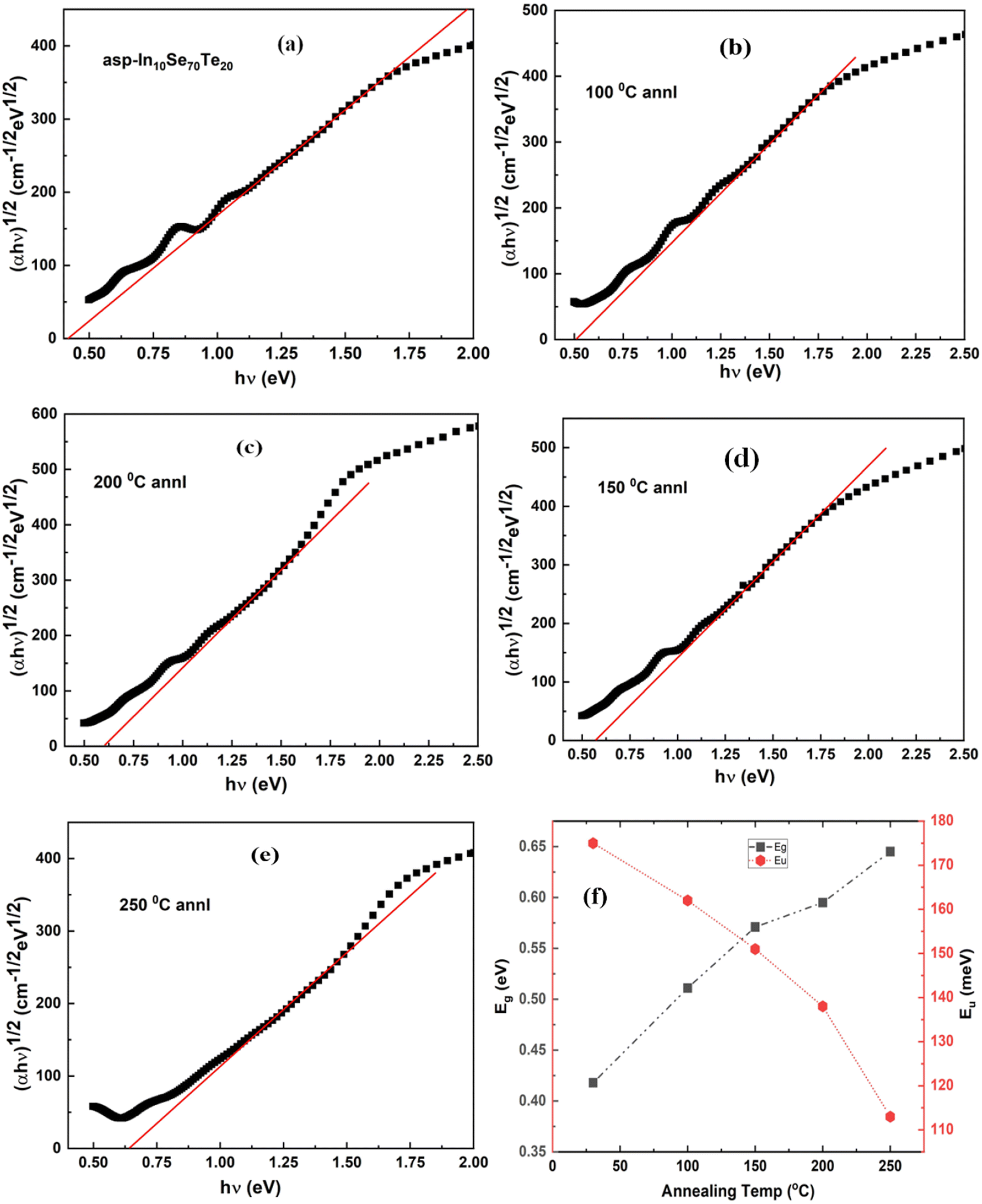 | ||
| Fig. 7 (a–e) Optical bandgap of as-deposited and annealed In10Se70Te20 films and (f) variation of Eg, which is the Urbach energy with annealing temperatures. | ||
| Optical parameter | As-prepared | 100 °C | 150 °C | 200 °C | 250 °C |
|---|---|---|---|---|---|
| Eg (eV) | 0.418 ± 0.03 | 0.511 ± 0.01 | 0.571 ± 0.01 | 0.595 ± 0.04 | 0.645 ± 0.02 |
| C1/2 (cm−1/2 eV−1/2) | 208 | 229 | 241 | 256 | 301 |
| EU (meV) | 175 | 162 | 151 | 138 | 113 |
| σ × 10−2 (steepness parameter) | 14.8 | 15.98 | 17.15 | 18.76 | 22.92 |
| Se–p | 4.504 | 4.172 | 3.887 | 3.554 | 2.909 |
| Ed (eV) | 0.1192 | 0.0804 | 0.0420 | 0.0371 | 0.0311 |
| Eo (eV) | 1.438 | 1.440 | 1.467 | 1.476 | 1.511 |
| f = EoEd | 0.1714 | 0.1157 | 0.0616 | 0.0547 | 0.0469 |
| M−1 | 0.0828 | 0.0558 | 0.0286 | 0.0251 | 0.0205 |
| M−3 | 0.0400 | 0.0269 | 0.0132 | 0.0115 | 0.00897 |
| n0 | 1.041 | 1.027 | 1.0142 | 1.0126 | 1.010 |
| ε∞ | 1.0836 | 1.0547 | 1.0286 | 1.0253 | 1.0201 |
| λo (nm) | 734.01 | 721.05 | 701.81 | 685.34 | 667.25 |
| S0 (nm2 × 10−8) | 12 | 6.6 | 4.3 | 3.7 | 3.5 |
| εL | 7.669 | 6.582 | 5.208 | 3.608 | 2.255 |
| N/m* (m−3 kg−1) × 1039 | 9.2 | 7.96 | 6.44 | 4.21 | 3.01 |
| Plasma frequency ω2 (×1011) | 8.67 | 8.74 | 8.94 | 9.13 | 9.65 |
| ηopt | 2.225 | 2.233 | 2.240 | 2.241 | 2.242 |
| χ1 (esu) × 10−3 | 6.65 | 4.35 | 2.27 | 2.01 | 1.60 |
| χ3 (hυ → 0) × 10−22 (esu) | 3324 | 608.7 | 45.13 | 27.74 | 11.14 |
| nT2 (esu) | 1.2 × 10⁻¹⁷ | 2.23 × 10⁻¹⁸ | 1.67 × 10⁻¹⁹ | 1.03 × 10⁻¹⁹ | 4.15 × 10⁻²⁰ |
| nF2 (esu) | 2.38 × 10⁻²⁰ | 1.05 × 10⁻²⁰ | 2.77 × 10⁻²¹ | 2.15 × 10⁻²¹ | 1.36 × 10⁻²¹ |
The Eg value of the as-prepared In10Se70Te20 film was 0.418 eV, which increased to 0.645 eV upon annealing at 250 °C temperature. The Eg values for the other films are shown in Table 2, which shows an increasing trend with annealing. The enhancement in Eg value with annealing is explained by the Mott and Davis theory.67 A large number of saturated bonds are formed by annealing unsaturated bonds at the above crystallization temperature. Such a decrease in unsaturated defects causes a reduction in the density of localized states in the gap and ultimately enhances the band gap.68 In other way, according to the chemical bond approach, the formation of greater bond energy-based bonds such as In–Se (53.64 kcal mol−1), Se–Te (44.18 kcal mol−1) and In–Te (33.05 kcal mol−1) occurs at first, followed by low energy-based bonds Te–Te (33 kcal mol−1) and Se–Se (44 kcal mol−1).49,69,70 The local structure in the film changed by bond breaking and bond arrangement due to annealing the thin films. Therefore, the low-energy bonds along with some dangling bonds were annealed with the formation of stronger bonds In–Se and In–Te bonds. This behaviour was also satisfied by the XRD and Raman studies. The formation of stronger saturated bonds in place of dangling bonds results in the reduction of the density of defect states over the gap region and enhances the band energy. Such effects bring changes in the absorption edge shift and reorganization at the atomic and molecular levels, modifying the optical parameters. According to Surbhi et al., the temperature dependency of the bandgap in semiconductors is often related to an increase in interatomic separation as the magnitude of atomic vibration rises with an increase in thermal energy, which leads to an increase in the electron–lattices interactions.71
The parameter C is an indicator of the degree of structural disorder for semiconducting materials. The value of C was evaluated from the slope of the fitting, as shown in Fig. 7a–e. The low value of C depicts more structural disorders.72 Thus, the higher C value (see Table 2) for the annealed films than for the as-deposited ones infers a reduction in structural disorder with annealing. Liu and colleagues studied the annealing-induced absorption and photoluminescence (PL) study of PbS QDs, which showed that an increase in annealing duration led to improved absorption and PL response.73 However, in our case, the annealing duration was kept at a fixed duration, i.e. 1.5 h, with varying temperatures in the range of 100–250 °C. Such variation in annealing temperature led to a reduction in the ‘α’ of the material. Similarly, Gami et al. synthesized (6,6)-phenyl C61 butyric acid methyl ester (PCBM)/Zinc(II) octaethylporphyrin (ZnOEP) thin film using the spin coating method. By varying the PCBM/ZnOEP thin film layer thickness, the Eg value was reduced, which is due to the creation of defects by the PCBM film. Thus, the Tauc parameter (B) was reduced, indicating that the PCBM content influenced the disorder of ZnOEP/PCBM.74 Surbhi et al. investigated the optical response of Te1−x(GeSe0.5)Scx (x = 0, 0.05, 0.1, and 0.15) (TGSS) thin films, which showed enhancement in the Eg with Sc doping. Here, the Tauc parameter (A) showed a reduction pattern as Sc increases, signifying the influence of doping in the TGSS film. This competition could be utilized for optical storage applications. The observed Eg range in TGSS is 1.18 eV–1.27 eV, which is slightly close to the currently observed values. Therefore, this In–Se–Te film might also be a possible application for optical storage applications.75 Furthermore, Dongol et al. investigated the annealing-induced optical properties of Ge20Se65S15 thin films, which showed a reduction pattern in the absorption coefficient with an increment in Eg from 2.07 eV to 2.13 eV. Such behavior is due to the creation of more numbers of saturated bonds in place of unsaturated bonds. Here, the Tauc parameter (B) value showed an increased trend, indicating a lower structural disorder with annealing. Such annealing-induced optical tuning in the Ge20Se65S15 thin film could be effectively used in photonic device fabrication.76
The presence of impurities and defects in the film results in a weak absorption region in which ‘α’ shows exponential variation with hν. Such an absorption edge indicates the existence of a localized state in the gap. The band tailing is due to random fluctuations in internal fields, causing structural disorders.77 The energy corresponding to this region is called the Urbach energy (EU), which is evaluated from Urbach's relation:78
 | (6) |
The broadening in the absorption edge is represented by the steepness parameter (σ), which is because of excitation due to electron–phonon or excitation–phonon interaction. This parameter is evaluated by the relation77 σ = KT/EU, where T is temperature, EU is the Urbach energy, and K is the Boltzmann constant. The obtained σ values are presented in Table 2 and shown in Fig. 8a, depicting an increase in σ with annealing. This confirms the increase in the optical bandgap due to the broadening of the gap.
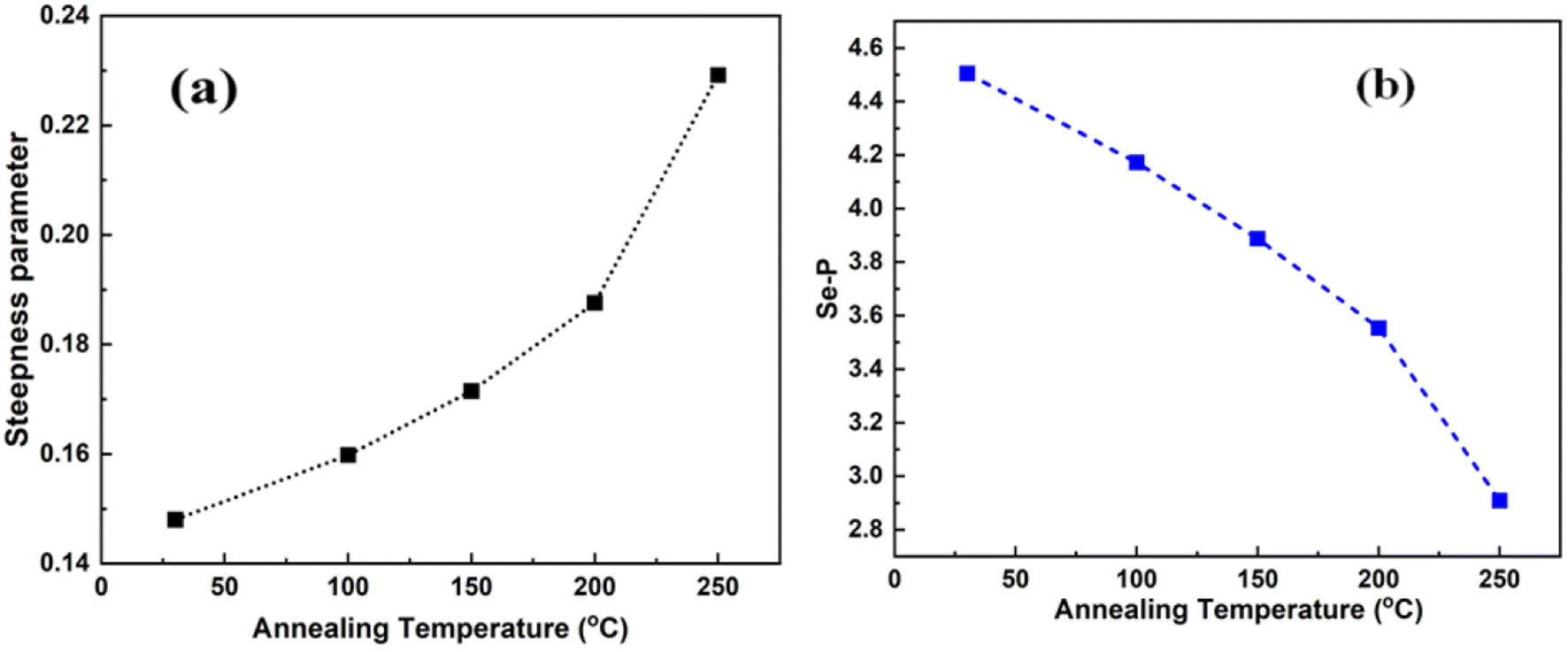 | ||
| Fig. 8 (a) Increase in steepness parameter and (b) decrease in Se–p value at different annealing temperatures. | ||
The interaction strength between electrons and phonons is represented by Se–p. The knowledge of lattice expansion and the increase in lattice constants is obtained from Se–p. The increase in Se–p value infers the increase in lattice dimensions and vice versa. The Se–p value is calculated by Se–p = 2/3σ,77 as demonstrated in Table 2. Considering that increasing the lattice dimensions leads to decreasing the band-gap energy, the decrease in the Se–p value with annealing results in an increase in the Eg value, as shown in Fig. 8b.
The decreased Se–p values are in good correlation with the increased Eg value because of their inverse relationship with each other. Because of the peculiar optical properties of In–Se–Te thin films, they are considered for many optoelectronic applications and devices, such as photonic circuits, photovoltaics, signal preparing, solar cells, optical fibers, photolithography, and optical recorders.
 | (7) |
Fig. 9a shows the refractive index change at different ‘λ’, showing the normal dispersion behaviour of the film. The value of ‘n’ decreased with annealing temperature with a simultaneous increase in Eg. In the lower wavelength regime, the ‘n’ value is large, whereas in the upper wavelength region, it decreases to a saturated value. The absorption capability is more at higher frequencies for which the speed of light decreases and the n-value increases. The optical field confinement is more at a high value of ‘n’, which maintains the small waveguides to bend inside the fibre. Thus, the optical intensities increase for which the material becomes more efficient and useful for non-linear interactions.80
 | ||
| Fig. 9 (a) Variation in ‘n’, (b) (n2 − 1)−1 vs. (hv)2 graph, (c) (n2 − 1)−1 vs. (λ)−2 graph and (d) n2 vs. λ2 graph of In10Se70Te20 thin films. | ||
The variation in refractive index is associated with the change in bandgap by Moss rule, i.e., Egn4 ∼ constant.81 The valence band is formed by lone pair orbitals, and the antibonding orbital forms the conduction band. With the increase in annealing temperature, there is excitation of bonding states and lone-pair electrons to the antibonding states. The vacancy created by this process is filled by the outer electrons and leads to the increase in lone-pair, holes and bonding orbitals, resulting in the formation of vacancy.61 Such bond rearrangement favors the local structure to change and reduces ‘n’ and ‘k’ values at higher annealing temperatures.
The dispersion parameters play an important role in designing various spectral dispersion and optical communication devices. Single oscillator (Eo) and dispersion (Ed) energy are two essential parameters for optical devices. The Ed is independent of Eo because Ed depends on the dielectric loss, whereas Eo does not depend on the dielectric loss. The Wemple-DiDomenico model is related to Eo, Ed and hν. Eo is regarded as the average energy gap that gives information on the band structure, while Ed carries the average inter band optical transition strength, in which the Ed value decreased because of the annealed films. It is related to structural parameter change in the material, such as coordination number (Nc), ionicity (β = 0.37 eV), the effective number of valence electrons per anion (Ne) and anion valency (Za) of the material by Ed = βNcZaNe (eV).76 The structural disorder and physical properties of the material are associated with ‘Ed’. The decreased value of Ed for the present case with annealing infers less structural disorder.
The single effective oscillator model provides an in-depth physical interpretation of the measured parameters. The model is presented by the following equation:54
 | (8) |
The calculations of Eo and Ed were performed from the graph between (n2 − 1)−1 vs. (hv)2, as depicted in Fig. 9b. The Eo and Ed values are evaluated from the slope and intercept of the fitting, as depicted in Table 2. It is noticed that Eo increased while Ed decreased with an increase in the annealing of In10Se70Te20 film. The lattice dielectric constant (ε∞) and static refractive index (n0) were calculated using the following formula:45,54
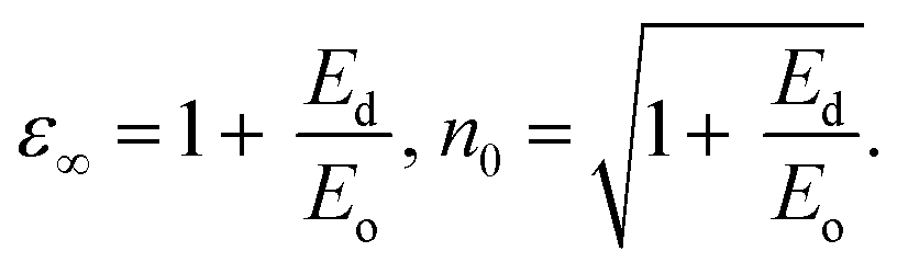 | (9) |
The quantity f = EoEd refers to the oscillator strength of the material, which decreased with an increase in annealing, as shown in Table 2. It is found that ε∞ decreased with annealing of In10Se70Te20 film.
The two moments of spectra first-order (M−1) and third-order (M−3) were evaluated by Eo and Ed using the following equations:45,52
| M−1 = Ed/Eo and M−3 = M−1/Eo2. | (10) |
The values of both M−1 and M−3 decreased with the annealing of In10Se70Te20 films, as shown in Table 2.
At the lower frequency region, the ‘n’ value satisfies the following Sellmeier's dispersion model:45,76
 | (11) |
The straight-line fitting of (n2 − 1)−1 vs. (λ)−2 (Fig. 9c) evaluates the value of ‘s0’ (strength of the oscillator) and λ0 (oscillator wavelength). The decreases in λ0 and s0 values with annealing of In10Se70Te20 films are shown in Table 2 λo is inversely proportional to Eo, and Eo is directly proportional to Eg, which leads to λo ∝ 1/Eg. Consequently, λo decreased due to the improvement in the crystallinity and change in the surface morphology of the films.82
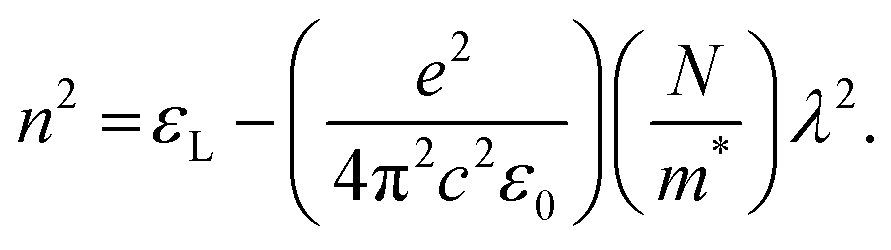 | (12) |
The plot between λ2 and n2, as presented in Fig. 9d, evaluates the value of N/m* and εL from its intercept and slope. The N/m* decreased from 9.2 × 1039 m−3 kg−1 of the as-prepared film to 3.01 × 1039 m−3 kg−1 for the 250 °C annealed film. This shows the microstructural changes in the film, as shown in Fig. 2. The change in the orientation of dipoles present in chalcogenide films led to variations in εL. Although both the values of εL and ε∞ are very close to each other, the decrease in both values upon annealing films is due to the increase in polarization.83 The lower value of ε∞ compared to εL is due to the contribution of free charge carriers to the polarization process, which has also been observed in other studies.84
The value of the plasma frequency (ωp) is evaluated using the following Drude relation:85

Or
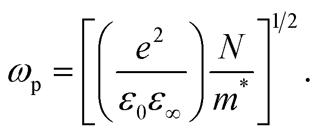 | (13) |
The calculated ωp values for the films are listed in Table 2. At the plasma frequency, the oscillation of free charge carriers achieves its peak. There is no other resonance except the plasma frequency, and the radiation of the material travels in the dielectric material and is reflected in the lower frequency. Here, ωp increased with thermal annealing for the studied films.
The dielectric constant is the built-in property of a semiconductor that defies the behavior under an applied electric field. The complex dielectric constant has both real (εr) and imaginary (εi) parts, ε* (=εr + iεi). Additionally, in terms of ‘n’ and ‘k’, it is expressed as ε* = (n + ik)2. The dielectric loss tangent (tan![[thin space (1/6-em)]](https://www.rsc.org/images/entities/char_2009.gif) δ) was evaluated from εr and εi. The εr gives an idea of the de-acceleration of incident energy during propagation inside the films. The ‘εi’ accounts for the loss of energy and is called the damping factor. This parameter measures the energy loss and dissipation inside the material during the passing of light waves inside it.85 The ratio εi/εr evaluates the loss factor, and these parameters are evaluated using the following formulas:85
δ) was evaluated from εr and εi. The εr gives an idea of the de-acceleration of incident energy during propagation inside the films. The ‘εi’ accounts for the loss of energy and is called the damping factor. This parameter measures the energy loss and dissipation inside the material during the passing of light waves inside it.85 The ratio εi/εr evaluates the loss factor, and these parameters are evaluated using the following formulas:85
| εi = 2nk and εr = n2 − k2. | (14) |
Fig. 10a and b show the variation in εr and εi with hv, and both parameters decreased with the annealing of In10Se70Te20 films. The comparatively high value of εr than εi is due to the changes in ‘n’ and ‘k’. The figures clearly show that the ‘ε1’ is seven times greater than the ‘ε2’. This is because n ≫ k in the ‘1’ case, whereas in the ‘ε2’ case, the low ‘k’ value reduced the imaginary part to less than 5.
 | ||
| Fig. 10 (a) εr vs. hν, (b) εi vs. hν, (c) tan(δ) vs. hν plot and (d) quality factor vs. hν plot for as-prepared and annealed In10Se70Te20 thin films. | ||
The dielectric loss factor measures the energy absorbed by the material when the electromagnetic wave passes inside it. This parameter also depicts the phase difference in the loss of energy at a fixed frequency (Fig. 10c). The value of ‘tanδ’ is more for the annealed film at high photon energy. The nature of change in tan(δ) is similar to the ‘k’ value, which infers the dominating nature of dielectric loss in this electromagnetic regime over optical absorption. The quality of oscillation so-called quality factor (Q)85 is the inverse of tan(δ), i.e. Q = εr/εi. The Q factor is found to decrease with the annealing of In10Se70Te20 films, as shown in Fig. 10d.
The moving electron losses energy while moving within the sample during its motion owing to plasma oscillations, which are excited in a sea of conduction band electrons. The degree of such loss of energy is associated with the optical features of any material. The energy loss functions are essential quantities for shedding light on damping on the surface or within the films. The average free path of the inelastic electron during its travel inside the sample is measured by such an energy loss function. Thus, it is essential to calculate the volume energy losses (VELF) and surface energy loss function (SELF). The VELF and SELF are evaluated using εr and εi as follows:82,85
 | (15) |
Both VELF and SELF define the absorption of energy of a material that signifies losses and is also related to a single transition of electrons in the semiconductor. The variation in VELF and SELF with λ is given in Fig. 11a and b, from which it is evident that VELF increased with annealing whereas SELF decreased with annealing.
 | ||
| Fig. 11 (a) Change in VELF, (b) SELF with hν, (c) variation in σr and (d) σr with hν for In10Se70Te20 films. | ||
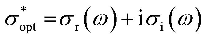 has both real and imaginary components. The σi (ω) = ωεoεr and σr (ω) = ωεoεi, where ω is the angular frequency. Fig. 11c and d show the variation in real and imaginary optical conductivities with photon energy. There is a rapid increase in both σi (ω) and σr (ω) as energy increases. This increment in both optical conductivities is explained by an increment in the absorption coefficient at a higher energy or lower wavelength. This behaviour has also been observed in other studies.75 Both values decreased upon annealing the In10Se70Te20 films.
The degree of polarization so called electrical susceptibility (χc) is denoted as follows:87
 | (16) |
The value of χc is shown in Fig. S3,† which indicates the decreasing trend with annealing and a higher value at a high value of hν.
The presence of lone pairs is linked with polarization by optical electronegativity (ηopt). The value of ηopt in terms of no is given as follows:86,87  where C = 25.54. The evaluated ηopt values increased with annealing for In10Se70Te20 films, as shown in Table 2. Because ηopt is related to the refractive index, the optical electronegativity also affects the non-linear parameters.
| P(t) = ε0[χ1E(t) + χ2E(t)2 + χ3E(t)3+…], | (17a) |
 | (17b) |
| χ(3) = A(χ(1))4 | (17c) |
The nonlinear refractive index is calculated from χ(3) using the Tichy and Ticha formula:88
 | (17d) |
The value of nT2 is found to decrease with the annealing of In10Se70Te20 films, as shown in Table 2. The nT2 value for the as-prepared In10Se70Te20 film decreased from 1.2 × 10⁻¹⁷ esu to 4.15 × 10⁻²⁰ esu for 250 °C annealing. Fornier and Snitzer correlated the nF2 and linear refractive index of the material using WDD parameters as follows:89
 | (17e) |
 | (17f) |
The estimated n2F using the Fornier and Snitzer models is presented in Table 2. The nF2 showed a lower value compared to nT2. The comparative plot presented in Fig. 12a showed that both nF2 and nT2 follow the same trend as that of the linear refractive index, i.e., overall decreased with an increase in annealing temperature. Furthermore, the change in Eg, χ3 and n2 under different annealing conditions is shown in Fig. S4.† The number of homopolar bonds decreased with an increase in heteropolar ones, thus decreasing the defects in the band structure. Therefore, the reduction in the density of defects and the decrease in the variety of defects account for the decrease in non-linearity with annealing. Lowering of χ(3) and n2 upon annealing is suitable for solid-state laser and UV non-linear materials.90
 | ||
| Fig. 12 (a) Variation in nF2 and nT2 and (b) βc with energy in In10Se70Te20 thin films. | ||
Two-photon absorption (TPA) is one of the most fundamental mechanisms that describes the procedure of induced absorption inside materials. This mechanism happens only when the energy of incident light is in the range of Eg/2 < hν < Eg. This TPA mechanism is described by the non-linear absorption coefficient (βc), which can be calculated using a simple empirical relation by Sheik Bahae et al.:75,91,92
 | (17g) |
The βc value showed greater magnitude at a lower energy and was then reduced. Fig. 12b shows the same pattern of βc as the non-linear parameters, i.e., increased with annealing temperature.
4. Conclusions
The findings from this study showed that annealing induced an increase in crystallinity and a decrease in dislocation density in In10Se70Te20 thin films. The particle size increased from 9.55 nm of the as-deposited one to 18.68 nm for the 250 °C annealed film. The structural change is due to the annealing out of the unsaturated bonds and defects in the film with heat energy, increasing the structural order. The In2Se3 and In2Te3 phase formation from the In10Se70Te20 film was confirmed by XRD and Raman studies. Surface morphological modification was noticed from the FESEM images, and the elemental mapping study showed a uniform distribution of elements in the film. The indirect allowed bandgap is found to be increased by 0.227 eV for the 250 °C annealed film from the as-deposited one. Such an increase in Eg is due to the increase in crystallinity and decrease in defects caused by annealing. The steepness parameter increased, and the Se–p value decreased with annealing. The effect of annealing temperature is observed on the dispersion and the non-linear parameters. The ‘k’ and ‘α’ values decreased by making the film more transparent upon annealing. The decrease in refractive index satisfies the Moss rule and results in an increase in Eo value by 0.073 eV and a decrease in Ed value by 0.0881 eV due to annealing. The oscillator strength, first and third moments of spectra, dielectric constant carrier concentration and oscillator wavelength decreased upon annealing. Simultaneously, plasma frequency increased from 8.67 to 9.65, and optical electronegativity increased with annealing temperature. Electrical susceptibility decreased along with optical conductivity. The non-linear refractive index decreased from 1.2 × 10⁻¹⁷ esu (as-prepared) to 4.15 × 10⁻²⁰ esu (250 °C), as did the non-linear susceptibility with annealing. The observed changes in the linear and non-linear optical parameters with annealing temperature are suitable for optoelectronic and non-linear optics.Author contributions
S. Giri: writing – original draft, software, data curation, investigation. P. Priyadarshini: experiment, data curation. D. Alagarasan: experiment, investigation. R. Ganesan: visualisation, investigation. R. Naik: conceptualization, methodology, writing – review & editing, supervision.Data availability
The data that support the findings of this study are available from the corresponding author upon reasonable request.Conflicts of interest
There are no conflicts of interest for this manuscript.Acknowledgements
R. Naik thanks ICT-IOCB for the Central Instrument facility.References
- M. H. R. Lankhorst, B. W. S. M. M. Ketelaars and R. A. M. Wolters, Low-cost and nanoscale and non-volatile memory concept for future silicon chips, Nat. Mater., 2005, 4, 347–352 CrossRef CAS PubMed.
- C. Tan, M. Amani, C. Zhao, M. Hettick, X. Song, D. H. Lien, H. Li, M. Yeh, V. R. Shrestha, K. B. Crozier, M. C. Scott and A. Javey, Evaporated SexTe1-x Thin films with tunable bandgaps for short-wave infrared photodetectors, Adv. Mater., 2020, 32, 2001329 CrossRef CAS PubMed.
- A. Rawat, A. Arora and A. De Sarkar, Interfacing 2D M2X (M= Na, K, Cs; X= O, S, Se, Te) monolayers for 2D excitonic and tandem solar cells, Appl. Surf. Sci., 2021, 563, 150304 CrossRef CAS.
- E. Colegrove, B. Good, A. Abbas, H. Moutinho, S. Johnston, C.-S. Jiang, P. O'Keefe, J. M. Walls, D. S. Albin and M. O. Reese, Investigating the role of copper in arsenic doped Cd (Se, Te) photovoltaics, Sol. Energy Mater. Sol. Cells, 2022, 246, 111886 CrossRef CAS.
- S. Maurugeon, B. Bureau, C. Boussard-Pledel, A. J. Faber, P. Lucas, X. H. Zhang and J. Lucas, Selenium modified GeTe4 based glasses optical fibers for far-infrared sensing, Opt. Mater., 2011, 33, 660–663 CrossRef CAS.
- I. Pethes, R. Chahal, V. Nazabal, C. Prestipino, A. Trapananti and S. Michalik, Chemical short-range order in selenide and telluride glasses, J. Phys. Chem. B, 2016, 120, 9204 CrossRef CAS PubMed.
- S. Cui, R. Chahal, C. Boussard-Pledel, V. Nazabal, J. L. Doualan, J. Troles, J. Lucas and B. Bureau, From selenium- to tellurium-based glass optical fibers for infrared spectroscopies, Molecules, 2013, 18, 5373–5388 CrossRef CAS PubMed.
- Y. Sung-Min, L. Nam-Yeal, R. Sang-Ouk, C. Kyu-Jeong, Y. S. Park, L. Seung-Yun, Y. Byoung-Gon, K. Myung-Jin, C. Se-Young and M. Wuttig, Sb–Se-based phase-change memory device with lower power and higher speed operations, IEEE Electron Device Lett., 2006, 27, 445–447 Search PubMed.
- Y. Lu, S. Song, X. Shen, L. Wu, Z. Song, B. Liu, S. Dai and Q. Nie, Investigation of Ga8Sb34Se58 material for low-power phase change memory, ECS Solid State Lett., 2013, 2, 94–96 CrossRef.
- R. Svoboda, M. Kincl and J. Malek, Thermal characterization of Se–Te thin films, J. Alloys Compd., 2015, 644, 40–46 CrossRef CAS.
- A. Zakery and S. R. Elliott, Optical properties and applications of chalcogenide glasses: a review, J. Non-Cryst. Solids, 2003, 330, 1–12 CrossRef CAS.
- A. A. Wilhelm, C. B. Pledel, Q. Coulombier, J. Lucas, B. Bureau and aP. Lucas, Development of far-infrared-transmitting Te based glasses suitable for carbon dioxide detection and space optics, Adv. Mater., 2007, 19, 3796–3800 CrossRef CAS.
- S. Raoux, W. Welnic and D. Ielmini, Phase change materials and their application to nonvolatile memories, Chem. Rev., 2010, 110, 240–267 CrossRef CAS PubMed.
- M. Wuttig and C. Steimer, Phase change materials: from material science to novel storage devices, Appl. Phys. A, 2007, 87, 411–417 CrossRef CAS.
- M. Wuttig and N. Yamada, Phase-change materials for rewriteable data storage, Nat. Mater., 2007, 6, 824–832 CrossRef CAS PubMed.
- W. Welnic, J. A. Kalb and D. Wamwangi, Phase change materials: from structures to kinetics, J. Mater. Res., 2007, 22, 2368–2375 CrossRef CAS.
- S. O. Kasap, T. Wagner, V. Aiyah, O. Krylouk, A. Bekirov and L. Tichy, Amorphous chalcogenide Se1-x-y TexPy semiconducting alloys: thermal and mechanical properties, J. Mater. Sci., 1999, 34, 3779–3787 CrossRef CAS.
- A. Kumar, M. Lal, K. Sharma, S. K. Tripathi and N. Goyal, Electrical properties of Se85-xTe15 Inx, Chalcogenide Lett., 2012, 9, 275–285 CAS.
- J. Sanghera, I. Aggarwal, L. Busse, P. Pureza, V. Nguyen, R. Miklos, F. Kung and R. Mossadegh, Development of low loss IR transmitting chalcogenide glass fibers, Proc. SPIE, 1995, 2396, 71 CrossRef.
- E. O. Wrasse, A. Torres, R. J. Baierle, A. Fazzio and T. M. Schmidt, Size effects induced high thermoelectric figure of merit in PbSe and PbTe nanowires, Phys. Chem. Chem. Phys., 2014, 16, 8114–8118 RSC.
- E. A. Banik and K. Biswas, Lead-free thermoelectrics: Promising thermoelectric performance in p-type SnTe1-xSex system, J. Mater. Chem. A, 2014, 2, 9620–9625 RSC.
- J. Zhen, W. Deng, C. Li, J. Feng, S. Zhang, S. Wan, G. Wang, H. Dong, R. A. Susilo and B. Chen, Superconductivity in In2Te3 under compression induced by electronic and structural phase transitions, J. Phys. Chem. Lett., 2022, 13, 1226–1233 CrossRef CAS.
- J. Yao, Z. Deng, Z. Zheng and G. Yang, Stable, Fast UV–Vis–NIR photodetector with excellent responsivity, detectivity, and sensitivity based on α-In2Te3 films with a direct bandgap, ACS Appl. Mater. Interfaces, 2016, 8, 20872–20879 CrossRef CAS PubMed.
- V. Sowjanya, K. V. Bangera and G. K. Shivakumar, Structural, electrical and optical properties of stoichiometric In2Te3 thin films, Ceram. Int., 2017, 43, 3748–3751 CrossRef CAS.
- N. Guettari, C. Amory, M. Morsli, J. C. Bernede and A. Khelil, InxTey semiconductor thin films obtained by co-evaporation, Thin Solid Films, 2003, 431–442, 497–501 CrossRef.
- Y. T. Huang, N. K. Chen, Z. Z. Li, X. P. Wang, H. B. Sun, S. Zhang and X. B. Li, Two-dimensional In2Se3: A rising advanced material for ferroelectric data storage, Info Mat., 2022, 4, 2341 Search PubMed.
- L. Wang, X. Wang, Y. Zhang, R. Li, T. Ma, K. Leng, Z. Chen, I. Abdelwahab and K. P. Loh, Exploring ferroelectric switching in α-In2Se3 for neuromorphic computing, Adv. Funct. Mater., 2020, 30, 2004609 CrossRef CAS.
- G. Almeida, S. Dogan, G. Bertoni, C. Giannini, R. Gaspari, S. Perissinotto, R. Krahne, S. Ghosh and L. Manna, Colloidal monolayer β-In2Se3 nanosheets with high photoresponsivity, J. Am. Chem. Soc., 2017, 139, 3005–3011 CrossRef CAS PubMed.
- W. Zheng, T. Xie, Y. Zhou, Y. L. Chen, W. Jiang, S. Zhao, J. Wu, Y. Jing, Y. Wu, G. Chen, Y. Guo, J. Yin, S. Huang, H. Q. Xu, Z. Liu and H. Peng, Patterning two-dimensional chalcogenide crystals of Bi2Se3 and In2Se3 and efficient photodetectors, Nat. Commun., 2015, 6, 6972 CrossRef CAS PubMed.
- S. R. Herd, K. Y. Ahn, R. J. Von Gutfeld and D. R. Vigliotti, Structural changes in Se-Te bilayers by laser writing, J. Appl. Phys., 1982, 53, 5 Search PubMed.
- S. M. Elkatlawy, A. H. El-Dosokey and H. M. Gomaa, Structural properties, linear, and non-linear optical parameters of ternary Se80Te(20–x) Inx chalcogenide glass systems, Bol. Soc. Esp. Ceram. Vidrio, 2020, 61, 203–209 CrossRef.
- N. S. Saxena, M. M. Imran and K. Singh, Simultaneous measurements of thermal conductivity and diffusivity of Se80Te20–xInx (x = 2, 4, 6 and 10) chalcogenide glasses at room temperature, Bull. Mater. Sci., 2002, 25, 241–245 CrossRef CAS.
- V. Sharma, A. Thakur, N. Goyal, G. Saini and S. Tripathi, Effect of In additive on the electrical properties of Se–Te alloy, Semicond. Sci. Technol., 2004, 20, 103 CrossRef.
- T. Akiyama, M. Uno, H. Kitaura, K. Narumi, R. Kojima and K. Nishiuchi, Rewritable dual-layer phase-change optical disk utilizing a blue-violet laser, Jpn. J. Appl. Phys., 2001, 40, 1598 CrossRef CAS.
- P. Priyadarshini, D. Sahoo, D. Alagarasan, R. Ganesan, S. Varadharajaperumal and R. Naik, Structural and optoelectronic properties change in Bi/In2Se3 heterostructure films by thermal annealing and laser irradiation, J. Appl. Phys., 2021, 129, 223101–223111 CrossRef CAS.
- R. Panda, S. A. Khan, U. P. Singh, R. Naik and N. C. Mishra, The impact of fluence dependent 120 MeV Ag swift heavy ion irradiation on the changes in structural, electronic, and optical properties of AgInSe2 nano-crystalline thin films for optoelectronic applications, RSC Adv., 2021, 11, 26218–26227 RSC.
- R. Panda, M. Panda, H. Rath, U. P. Singh, R. Naik and N. C. Mishra, annealing induced AgInSe2 formation from Ag/In/Ag/In multilayer film for solar cell absorbing layer, Opt. Mater., 2018, 84, 618–624 CrossRef CAS.
- D. Sahoo, S. Sahoo, D. Alagarasan, R. Ganesan, S. Varadharajaperumal and R. Naik, Proton ion irradiation on As40Se50Sb10 thin films: Fluence-dependent tuning of linear–Non-linear optical properties for photonic applications, ACS Appl. Electron. Mater., 2022, 4, 856–868 CrossRef CAS.
- R. Panda, R. Naik and N. C. Mishra, Low-temperature growth of γ phase in thermally deposited In2Se3 thin films, Phase Trans., 2019, 91, 862–871 CrossRef.
- H. P. Pathak, N. Shukla, V. Kumar and D. K. Dwivedi, Structural and optical properties of In doped Se–Te phase-change thin films: a material for optical data storage, Opt. Mater., 2016, 52, 69–74 CrossRef CAS.
- Y. H. Abdelalim, A. H. A. Sakr, S. M. El-Ghanam and M. A. Hamad, Tailoring of optical properties of Se80Te20-xInx films by annealing process, Appl. Phys. A, 2022, 128, 643 CrossRef CAS.
- A. M. Abd-Elnaiem, S. Moustafa, A. M. Abdelraheem, M. A. Abdel-Rahim and A. Z. Mahmoud, Effects of Annealing on structural and optical properties of Ge20Se70Sn10 thin films for optoelectronic applications, J. Non-Cryst. Solids, 2020, 549, 120353 CrossRef CAS.
- M. Rashad, R. Amin, S. A. Al-Ghamdi, M. M. Hafiz and A. M. Abd-Elnaiem, Improving the electrical parameters of Se80Te20 films by the Sn substitution for Te and thermal-induced effect, J. Electron. Mater., 2021, 50, 2075–2082 CrossRef CAS.
- H. Sing, S. Kumari, P. Singh, A. Kumar and A. Thakur, Effect of Annealing on structural, morphological and optical properties of InSe thin films, J. Mater. Sci.: Mater. Electron., 2022, 33, 23599–23606 CrossRef.
- A. Parida, D. Sahoo, D. Alagarasan, S. Vardhrajperumal, R. Ganesan and R. Naik, Increase in non-linear susceptibility and refractive index in quaternary In15Sb10S15Se60 thin films upon annealing at different temperature for photonic applications, J. Alloys Compd., 2022, 905, 164143 CrossRef CAS.
- S. Das, S. Senapati, D. Alagarasan, S. Vardhrajperumal, R. Ganesan and R. Naik, Enhancement of non-linear optical parameters upon phase transition in new quaternary Ge20Ag10Te10Se60 films by annealing at various temperatures for optoelectronic applications, J. Alloys Compd., 2022, 927, 167000 CrossRef CAS.
- S. Sharma, R. Sharma, P. Kumar, R. Thangaraj, K. Ashokan and M. Mian, Structural, optical and photoelectrical properties of thermally annealed amorphous In15Sb15Se70 chalcogenide films, Appl. Phys. A, 2018, 124, 357 CrossRef.
- A. Harizia, M. B. Rabeha, F. Laatarb, F. C. Akkaria and M. Kanzaria, Substrate temperature dependence of structural, morphological and optical properties of Sn4Sb6S13 thin films deposited by vacuum thermal evaporation, Mater. Res. Bull., 2016, 79, 52–62 CrossRef.
- P. Priyadarshini, S. Das, D. Algarasan, R. Ganesan, S. Varadharajaperumal and R. Naik, Role of Bismuth incorporation on the structural and optical properties in BixIn35-xSe65 thin films for photonic applications, J. Am. Ceram. Soc., 2021, 104, 5803–5814 CrossRef CAS.
- J. Weszka, Ph. Daniel, A. Burian, A. M. Burian and A. T. Nguyen, Raman scattering in In2Se3 and InSe2 amorphous, J. Non-Cryst. Solids, 2000, 265, 98–104 CrossRef CAS.
- C. H. Ho, Amorphous effect on the advancing of wide-range absorption and structural-phase transition in γ-In2Se3 polycrystalline layers, Sci. Rep., 2014, 4, 4764 CrossRef PubMed.
- S. Das, P. Priyadarshini, D. Alagarasan, S. Vardhrajperumal, R. Ganesan and R. Naik, Structural, morphological, and linear/non-linear optical properties tuning in Ag60-xSe40Tex films by thermal annealing for optoelectronics, J. Non-Cryst. Solids, 2022, 592, 121742 CrossRef CAS.
- I. Childres, J. Tian, I. Mitokowski and Y. Chen, AFM and Raman studies of topological insulator materials subject to argon plasma etching, Philos. Mag., 2013, 93, 681–689 CrossRef CAS.
- G. Abbady, A. Qasem and A. M. Abd-Elnaiem, Optical parameters and electronic properties for the transition of the amorphous-crystalline phase in Ge20Te80 thin films, J. Alloys Compd., 2020, 842, 155705 CrossRef CAS.
- A. M. Adam, E. Lilov, V. Lilova and P. Petkov, Characterization and optical properties of bismuth chalcogenide films prepared by pulsed laser deposition technique, Mater. Sci. Semicond. Process., 2017, 57, 210–219 CrossRef CAS.
- D. Sahoo, P. Priyadarshini, A. Aparimita, D. Alagarasan, R. Ganesan, S. Varadharajaperumal and R. Naik, Role of annealing temperature on optimizing the linear and non-linear optical properties of As40Se50Ge10 films, RSC Adv., 2020, 10, 26675–26685 RSC.
- H. Nyakotyo, T. S. Sathiaraj and E. Muchuweni, Effect of Annealing on the optical properties of amorphous Se79Te10Sb4Bi7 thin films, Opt. Laser Technol., 2017, 92, 182–188 CrossRef CAS.
- R. K. Pan, H. Z. Tao, H. C. Zang, X. J. Zhao and T. J Zhang, Annealing effects on the structure and optical properties of GeSe2 and GeSe4 films prepared by PLD, J. Alloys Compd., 2009, 484, 645 CrossRef CAS.
- S. Mishra, P. K. Singh, P. Lohia and D. K. Dwivedi, Thin film preparation and optical properties of Se–Te based chalcogenide glasses for optoelectronic applications, Glass Phys. Chem., 2020, 46, 341–349 CrossRef.
- A. A. A. Darwish and H. A. M. Ali, On annealing induced effect in optical properties of amorphous GeSeSn chalcogenide films for optoelectronic applications, J. Alloys Compd., 2017, 710, 431–435 CrossRef CAS.
- A. A. Al-Ghamdi, S. A. Khan, S. Al-Heniti, F. A. Al-Agel and M. Zulfequar, Effects of laser irradiation on optical properties of amorphous and annealed Ga15Se81In4 and Ga15Se79In6 chalcogenide thin films, J. Alloys Compd., 2010, 505, 229–234 CrossRef CAS.
- A. A. Al-Ghamdi, S. A. Khan, S. Al-Heniti, F. A. Al-Agel and M. Zulfequar, Annealing and laser irradiation effects on optical constants of Ga15Se85 and Ga15Se83In2 chalcogenide thin films, Curr. Appl. Phys., 2011, 11, 315–320 CrossRef.
- A. Parida, D. Sahoo, D. Alagarasan, S. Varadharajaperumal, R. Ganesan and R. Naik, Impact on non-linear/linear optical and structural parameters in quaternary In15Ag10S15Se60 thin films upon annealing at different temperatures, Ceram. Int., 2022, 48, 15380–15389 CrossRef CAS.
- P. Priyadarshini, S. Das, D. Alagarasan, R. Ganesan, S. Varadharajaperumal and R. Naik, Annealing induced modification in linear and non-linear optical properties of Bi7In28Se65 thin films for non-linear applications, Opt. Mater., 2021, 122, 111801 CrossRef CAS.
- A. S. Hassanien and I. Sharma, Band-gap engineering, conduction and valence band positions of thermally evaporated amorphous Ge15-xSbxSe50Te35 thin films: Influences of Sb upon some optical characterizations and physical parameters, J. Alloys Compd., 2019, 798, 750–763 CrossRef CAS.
- J. Tauc and A. Menth, States in the gap, J. Non-Cryst. Solids, 1972, 8, 569–585 CrossRef.
- N. F. Mott and E. A. Davis, Electronic Processes in Non-Crystalline Materials, Clarendon Press, Oxford, 1979, p. 210 Search PubMed.
- A. El-Korashy, A. Bakry, M. A. Abdel-Rahim and M. Abd El-Sattar, Annealing effects on some physical properties of Ge5Se25Te70 chalcogenide glasses, Phys. B, 2007, 391, 266–273 CrossRef CAS.
- K. A. Aly, N. Afify, A. M. Abousehlly and A. M. Abd Elnaeim, Optical band gap and refractive index dispersion parameters of In–Se–Te amorphous films, J. Non-Cryst. Solids, 2011, 357, 2029–2034 CrossRef CAS.
- S. Das, P. Priyadarshini, D. Alagarasan, S. Vardhrajperumal, R. Ganesan and R. Naik, Role of tellurium addition on the linear and non-linear optical, structural, morphological properties of Ag60-xSe40Tex thin films for non-linear applications, J. Am. Ceram. Soc., 2022, 105, 3469–3484 CrossRef CAS.
- S. Agarwal, P. Lohia and D. K. Dwivedi, Emerging phase change memory devices using non-oxide semiconducting glasses, J. Non-Cryst. Solids, 2022, 597, 121874 CrossRef CAS.
- R. K. Pan, H. Z. Tao, H. C. Zang, X. J. Zhao and T. J. Zhang, Annealing effects on the structure and optical properties of GeSe2 and GeSe4 films prepared by PLD, J. Alloys Compd., 2009, 484, 645 CrossRef CAS.
- C. Liu, Y. K. Kwon and J. Hao, Absorption and photoluminescence of PbS QDs in glasses, J. Non-Cryst. Solids, 2009, 355, 1880–1883 CrossRef CAS.
- F. Gami, I. Guizani, M. A. Sebak, A. A. Abuelwafa and M. M. Mostafa, Investigation of structural, optical and electrical properties of PCBM/ZnOEP thin films, Opt. Mater., 2022, 134, 113093 CrossRef CAS.
- S. Agarwal, P. Lohia and D. K. Dwivedi, Study of optical parameters of Te(1-x) (GeSe0.5) Scx (0 ≤ x ≤ 0.15) thin films for optical data storage applications, J. Non-Cryst. Solids, 2023, 606, 122199 CrossRef CAS.
- M. Dongol, A. F. Elhady, M. S. Ebied and A. A. Abuelwafa, Effect of thermal Annealing on the optical properties of Ge20Se65S15 thin films, Ind. J. Phys., 2021, 95, 1245–1253 CrossRef CAS.
- A. Srivastava, S. N. Tiwari and M. A. Alvi, Phase change studies in Se85In15−xZnx chalcogenide thin films, J. Appl. Phys., 2018, 123, 125105 CrossRef.
- F. Urbach, The long-wavelength edge of photographic sensitivity and of the electronic absorption of solids, Phys. Rev., 1953, 92, 1324 CrossRef CAS.
- S. Yaseem, F. Iqbal, T. Munawar, M. A. Nawaz, M. Asghar and A. Hussain, Synthesis, structural and optical analysis of surfactant assisted ZnO–NiO nanocomposites prepared by homogeneous precipitation method, Ceram. Int., 2019, 45, 17859–17873 CrossRef.
- I. Sharma, S. K. Tripathi and P. B. Barman, Effect of Bi addition on the optical behavior of a-Ge-Se-In-Bi thin films, Appl. Surf. Sci., 2008, 255, 2791–2795 CrossRef CAS.
- T. S. Moss, A relationship between the refractive index and the infra-red threshold of sensitivity for photoconductors, Proc. Phys. Soc., London, Sect. B, 1950, 63, 167–176 CrossRef.
- A. S. Hassanien and A. A. Akl, Optical characterizations and refractive index dispersion parameters of annealed TiO2 thin films synthesized by RF-sputtering technique at different flow rates of the reactive oxygen gas, Phys. B, 2020, 576, 411718 CrossRef CAS.
- A. El-Denglawey, M. Makhlouf and M. Dongol, The effect of thickness on the structural and optical properties of nano Ge-Te-Cu films, Res. Phys., 2018, 10, 714–720 Search PubMed.
- A. Bute, S. Jena, R. Sharma, D. Udupa and N. Maiti, Linear and non-linear optical properties of boron carbide thin films, Appl. Surf. Sci., 2023, 608, 155101 CrossRef CAS.
- A. S. Hassanien and I. Sharma, Optical properties of quaternary a-Ge15-xSbxSe50Te35 thermally evaporated thin-films: refractive index dispersion and single oscillator parameters, Optik, 2020, 200, 163415 CrossRef CAS.
- A. S. Hassanien and I. Sharma, Dielectric properties, Optoelectrical parameters and electronic polarizability of thermally evaporated a-Pb-Se-Ge thin films, Phys. B, 2021, 622, 413330 CrossRef CAS.
- D. Sahoo, D. Alagarasan, R. Ganesan, S. Varadharajaperumal and R. Naik, Impact of irradiation doses on the structural, morphological, and linear-nonlinear optical properties of Ge10Sb25Se65 thin films for optoelectronic applications, Eur. Phys. J. Plus, 2022, 137, 707 CrossRef CAS.
- L. Tichý, H. Ticha, P. Nagels, R. Callaerts, R. Mertens and M. Vlcek, Optical properties of amorphous As-Se and Ge-As-Se thin films, Mater. Lett., 1999, 39, 122–128 CrossRef.
- S. Mishra, P. K. Singh, R. K. Yadav, A. Kumar, P. Lohia and D. K. Dwivedi, Investigation of glass forming ability, linear and non-linear optical properties of Ge-Se-Te-Sb thin films, Chem. Phys., 2021, 541, 111021 CrossRef CAS.
- X. Dong, L. Huang, Q. Liu, H. Zeng, Z. Lin, D. Xu and G. Zou, Perfect balance harmony in Ba2NO3(OH)3: a beryllium-free nitrate as a UV non-linear optical material, Chem. Commun., 2018, 54, 5792–5795 RSC.
- A. A. Abuelwafa, M. S. Abd El- sadek, S. Elnobi and T. Soga, Effect of transparent conducting substrates on the structure and optical properties of tin (II) oxide (SnO) thin films: Comparative study, Ceram. Int., 2021, 47, 13510–13518 CrossRef CAS.
- A. A. Abuelwafa, H. M. Alsoghier, S. Elnobi, M. Dongol and T. Soga, Quantum computational, linear and non-linear optical properties of spin-coated nickel (II)-tetraphenylporphyrin/FTO thin films, Optik, 2021, 234, 166618 CrossRef CAS.
Footnote |
| † Electronic supplementary information (ESI) available. See DOI: https://doi.org/10.1039/d3ra03731b |
| This journal is © The Royal Society of Chemistry 2023 |