
 Open Access Article
 This Open Access Article is licensed under a Creative Commons Attribution-Non Commercial 3.0 Unported Licence
Investigation of Al droplet wetting behavior on highly-oriented SiC†
Song Zhang a,
Kaixin Zuob,
Pengjian Lubc,
Qingfang Xu*a,
Meijun Yanga,
Kai Liub and
Rong Tuad
a,
Kaixin Zuob,
Pengjian Lubc,
Qingfang Xu*a,
Meijun Yanga,
Kai Liub and
Rong Tuad
aState Key Laboratory of Advanced Technology for Materials Synthesis and Processing, Wuhan University of Technology, 122 Luoshi Road, Wuhan 430070, People's Republic of China. E-mail: xuqingfanghed@163.com
bSchool of Materials Science and Engineering, Wuhan University of Technology, 122 Luoshi Road, Wuhan 430070, People's Republic of China
cWuhan Tuocai Technology Co., Ltd, 147 Luoshi Road, Wuhan 430070, People's Republic of China
dChaozhou Branch of Chemistry and Chemical Engineering Guangdong Laboratory, Chaozhou 521000, People's Republic of China
First published on 7th September 2023
Abstract
In the integrated circuit industry, metal liquids are frequently in contact with chemical vapor deposited (CVD) SiC, and it is important to understand the interactions between CVD-SiC and metal droplets. In this study, the wetting behavior of Al on a highly oriented SiC surface was investigated, and the contact angle could be controlled from 6° to 153° at a wetting temperature (Twet) of 1573–1773 K; the obtained contact angle range was larger than that of polycrystalline silicon carbide (Twet = 873–1473 K, 9–113°) and single crystal silicon carbide (Twet = 873–1473 K, 31–92°). The presence of many dislocations at the Al/SiC interface increased the interfacial energy, resulting in a greater contact angle for Al on the 〈111〉-oriented SiC coating surface than on the 〈110〉 one.
1. Introduction
Al is commonly used as a metal material for computing storage hard drives, preparing p-type semiconductors, etc.,1–3 and is usually prepared by zone melting in a vacuum using SiC as a container.4 CVD-SiC is an excellent covalent material with high purity,5 high melting point, high hardness,6 and corrosion resistance7,8 and containers with CVD-SiC coatings can be used in the Integrated Circuit (IC) industry. The wettability requirements for silicon carbide surfaces vary in different application scenarios. When silicon carbide is used as a vehicle or as a container, a poorly wetted surface is required for better surface cleaning.9–11 When silicon carbide is used as a metal matrix reinforced composite material, a poorly wetted surface is required for better bonding properties between the metal matrix material and the silicon carbide. By controlling the wetting behavior of aluminum droplets on highly orientated SiC coatings, the flow and adherence of droplets on the surface of the SiC coatings can be controlled.Many studies on the wettability of Al/SiC systems have been conducted, and these studies have revealed the severe inconsistency of the claimed equilibrium contact angles at the same wetting temperature, as illustrated in Fig. 1, mostly because of the various SiC substrate types used in these studies. In the case of SiC single crystal,12–16 Shen et al.15 have demonstrated that the wettability of SiC was influenced by its surface polarity. The contact angle on the C-terminated surface is smaller than that on the Si-terminated surface of the (0001) crystal plane. At the Al/C-terminated SiC junction, strong covalent bonds were formed via orbital hybridization and charging distribution, whereas at the Al/Si-terminated SiC interface, metallic or ionic bonds were formed. The effect of the crystal surface ((110) and (111)) on the wetting characteristics was simulated using classical molecular dynamics.14 The findings demonstrate that the contact angle of the (110) system is 97.35° larger than that of the (111) system, which is 107.32°. However, studies on the wettability of Al/SiC ceramic polycrystalline systems have focused on reducing the contact angle of Al/SiC systems by integrating alloying elements with Al or modifying the SiC surface coating.17,18 Cong et al.18 examined the impact of adding alloying elements and their temperature on wettability, and showed that increasing the temperature or adding a sufficient amount of Si to Al (Al-12 wt% Si) significantly reduced the contact angle of the system (from 72° to 38° at 1173 K). However, the wettability behavior of Al droplets on SiC polycrystals remains unclear. In this study, CVD-SiC was used as a substrate to obtain a larger range of contact angles than in previous studies. The surface structure of the CVD-SiC coating and the effect of crystal orientation on wettability were also revealed.
 | ||
| Fig. 1 Contact angles for the Al/SiC as a function of temperature in reported literature. | ||
2. Experimental
Chemical vapor deposition was employed to create the SiC coatings that were used in the experiments9,19,20 with pure Al (99.999 wt%) as the metal specimen. Table 1 provides the deposition conditions (deposition temperature Tdep, total pressure Ptot) of each sample. Before the start of the experiment, CVD-SiC was pretreated by dipping in acetone and ethanol sequentially and ultrasonically cleaning for 15 min to remove surface impurities and ensure the cleanliness of the substrate. Then, the cleaned substrate is put into the oven and dried at 333 K for 20 min. High-temperature wetting experiments were conducted using a high-temperature contact angle measuring instrument SDC-1500 (Dongguan Dingsheng Precision Instruments Co., Ltd). The schematic diagram of the contact angle measuring equipment is shown in Fig. 2(a)–(f) shows an image of the morphological changes in the metal Al sample during the wetting process. Cylindrical pure Al particles (φ 3 × 3 mm) were placed on a CVD-SiC coating (15 × 15 × 2 mm) and heated up at a rate of 10 K min−1. When the Al drops started to melt, photos were taken using a charge-coupled device (CCD) camera. The droplet distribution was subsequently recorded at regular intervals during the wetting process, and contact angle values were calculated for droplet profile analysis. The entire procedure was performed in a vacuum at a pressure of approximately 10−4 Pa.| Sample | A | B | C |
|---|---|---|---|
| Tdep (K) | 1773 | 1873 | 1873 |
| Ptot (kPa) | 5 | 5 | 4 |
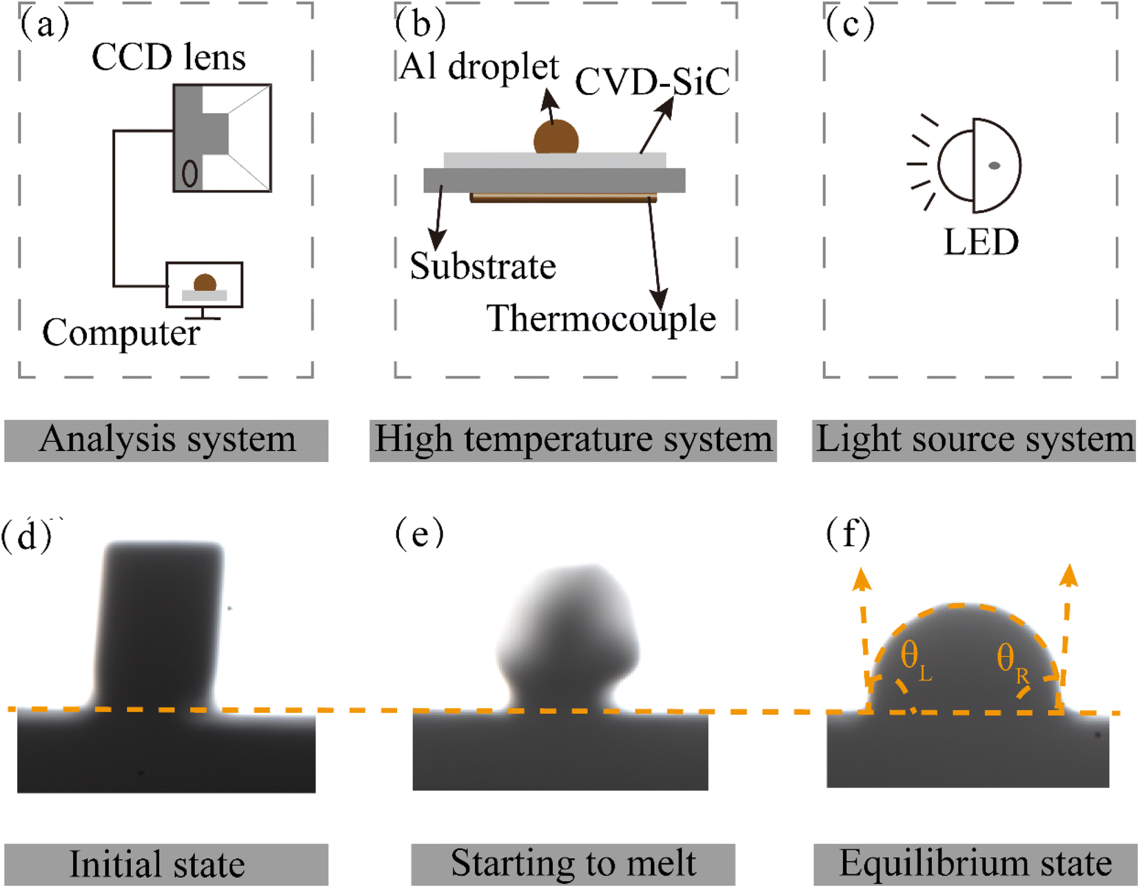 | ||
| Fig. 2 (a–c) Are schematic diagrams of the contact angle measuring device and (d)–(f) are image changes of pure Al during the wetting experiment. | ||
To determine the crystal phase and preferred orientation, X-ray diffraction (XRD; θ–2θ; Cu-Kα radiation; Ultima III) analysis was performed. Surface and cross-sectional microstructural analyses of the samples were performed using a scanning electron microscopy instrument (SEM; Quanta-250) operating at 20 kV. The microstructure of the Al/SiC interface was evaluated using transmission electron microscopy (TEM; Talos F200S), and the lattice mismatch at the interface was used to evaluate the difference in wettability at the interface.
3. Results and discussion
The contact angle is usually used to measure the wettability, when the contact angle is greater than 90° becomes non-wetting, when the contact angle is less than 90° becomes wetting, ideal surface, the contact angle satisfies the Young's equation: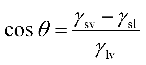 (γsv is the free energy at the solid–gas interface, γsl is the free energy at the solid–liquid interface, γlv is the free energy at the gas–liquid interface).
Fig. 3 shows the equilibrium contact angle of pure Al at different wetting temperatures on the surface of samples A, B and C at different wetting temperatures (Twet). The magnitude of the equilibrium contact angle on the same CVD-SiC coated surface decreases with increasing wetting temperature. The magnitude of the equilibrium contact angle at the same wetting temperature is related to the different types of CVD-SiC substrates.
 | ||
| Fig. 3 Equilibrium contact angles of pure aluminium on the surfaces of samples A, B and C at different wetting temperatures (Twet). | ||
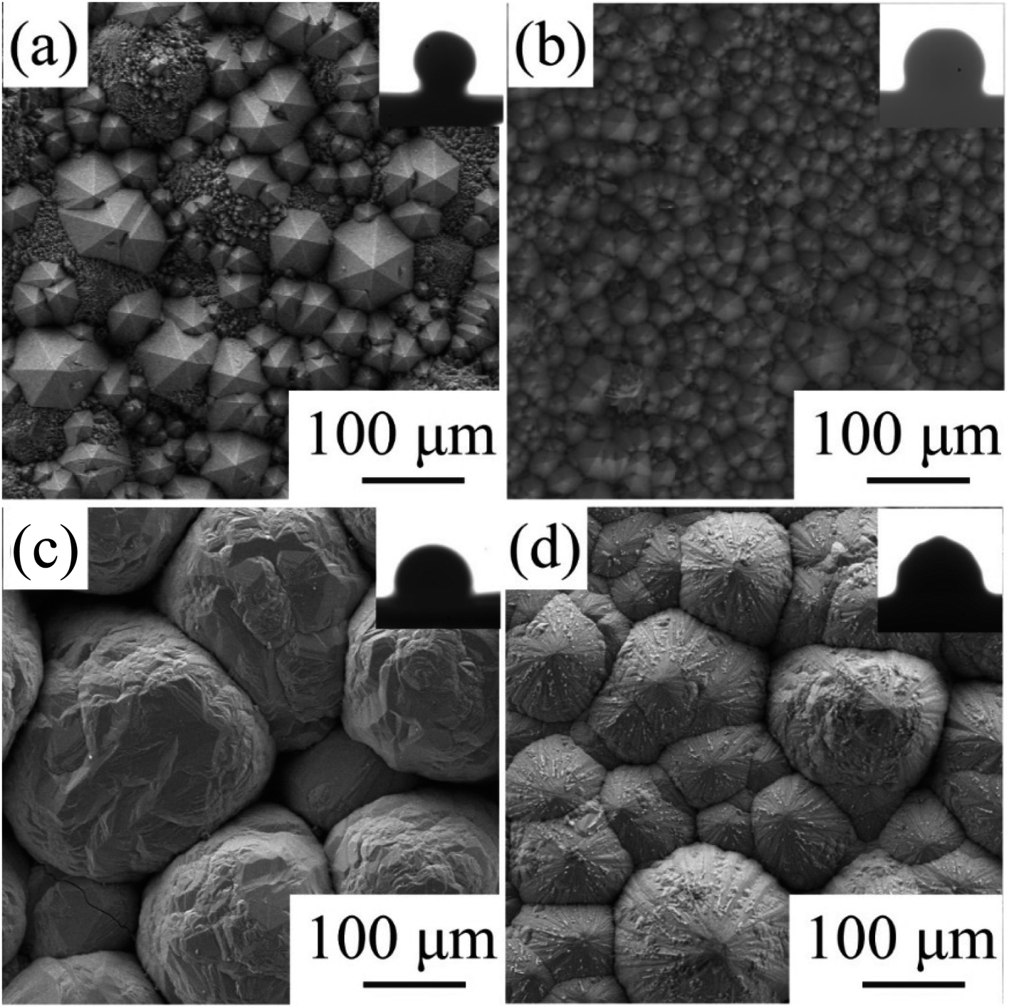
The CVD-SiC coatings obtained at various deposition temperatures and total gas pressures are shown in Fig. 4 in cross-sectional and surface SEM images. At Tdep = 1773 K, Ptot = 5 kPa, Fig. 4(a) and (d) show a six-fold pyramid structure of sample A, which is attributed to the 3C-SiC six-fold symmetry {111} surface, which grows perpendicular to the surface of the substrate; the cubic phase structure of silicon carbide is what causes the pyramidal grains, which are typical for the 〈111〉 orientation; to have a six-fold symmetry, the edge of the pyramid may be bidirectional domain boundary (DPB) or a twin boundary (TB).19 Fig. 4(b) and (e) show the cauliflower-like structures of sample B at Tdep = 1873 K and Ptot = 5 kPa because the competing growth of grains with different orientations results in the surface failing to appear as a regular polyhedron. The mirror-like structure of sample C (Fig. 4(c) and (f)) of the CVD-SiC coating deposited at Tdep = 1873 K and Ptot = 4 kPa is obtained because the nucleation rate during deposition is faster than the grain growth rate, which result in a flatter mirror-like structure owing to the inability of the grains to grow.9
 | ||
| Fig. 4 Cross-section and surface SEM images of samples A, B, C. (a) and (d), sample A, (b) and (e), sample B, (c) and (f), sample C. | ||
Fig. 5(a) shows the variation in the contact angle of pure Al at Twet = 1573 K on the surfaces of the three CVD-SiC coatings, and Fig. 5(b) shows a schematic diagram of the change in droplet shape during the wetting of pure Al. The abovementioned Fig. 5(a) demonstrates that the contact angle of pure Al at final equilibrium on the surface of sample A was 153.8°, and the final contact angle on the samples B and C were 120.6° and 101.2°, respectively. As the image illustrates the wetting of Al on the surface of the CVD-SiC coating can be divided into three stages. Stages I and II are collectively referred to as the linear spreading stages of the Al droplets on the surface of the CVD-SiC coating. The contact diameter of the droplet with the CVD-SiC surface linearly increased, whereas the droplet height and contact angle linearly decreased until the end of the spreading phase. The spreading rate of the first stage was higher than that of the second stage, probably because of the self-cleaning reaction of Al (Al(l) + Al2O3 = Al2O(g))15 in the first stage, which accelerates the spreading rate of the Al droplets. The Al droplets at high temperatures were accompanied by a certain amount of evaporation for an extend period of time. The contact diameter, droplet height and contact angle of the Al droplets with the CVD-SiC coating surface were slightly reduced until the end of the process, which was the third stage of Al droplet wetting on the CVD-SiC coating surface.
 | ||
| Fig. 5 Variation of (a) contact angle at Twet = 1573 K. Schematic diagram of Al droplet shape change during the wetting process (b). | ||
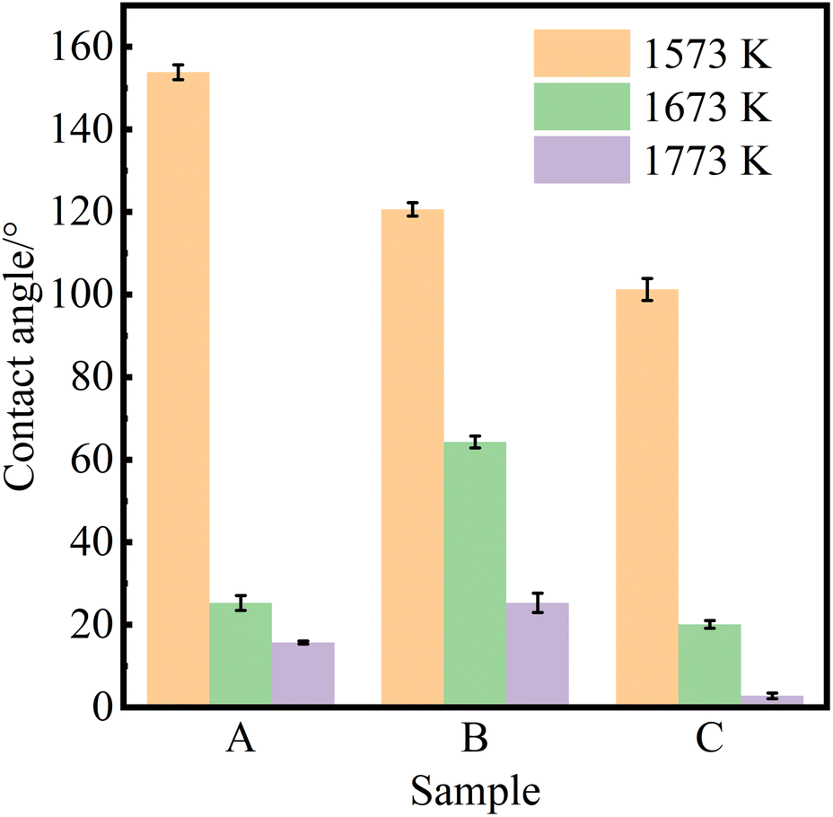
After the wetting experiment is completed and cooled to room temperature, the samples are removed. To obtain surface and cross-sectional scan images of the Al/SiC interface, it was cut along the top using a diamond cutter. (Note here that the contact angle of pure Al on the surface of sample A is 153.8° and that the Al droplets can easily be separated from the CVD-SiC sample during the cutting process.) The surface and cross section of the Al/SiC interface as observed using SEM is shown in Fig. 6.
 | ||
| Fig. 6 Cross-section and surface SEM images after wetting for 10 min at Twet = 1573 K, (a)–(c), sample A, (d)–(f), sample B, (g)–(i), sample C, (j)–(r) interfacial EDS spectra of sample B and C at Twet = 1573 K wetted for 10 min. | ||
Fig. 6 shows surface and cross-sectional images and matching EDS energy spectra after 10 min of wetting at Twet = 1573 K. The results show that no Al droplets were observed on the surface of Fig. 6(a)–(c) because the Al droplets have a wetting angle of 153.8° on the surface of the sample A and are easily separated from the CVD-SiC. However, there is a clear demarcation between the Al droplets and the CVD-SiC coating in Fig. 6(d)–(i), indicating a clear adhesion of the Al droplets between the CVD-SiC coating. Fig. 6(j)–(r) show the elemental distribution maps of the Al droplets at the sample B and sample C wetting interface. The image shows that the distribution of Al droplets is filling the grooves of the CVD-SiC coating, which is a “wet contact” and is applicable to the “Wenzel” model; under the “Wenzel” model, the apparent contact angle of the non-uniform surface is related to the intrinsic contact angle, as follows:21
cos![[thin space (1/6-em)]](https://www.rsc.org/images/entities/char_2009.gif) θr = rcosθ θr = rcosθ |
where Sr and S denote the surface and the projected areas of the CVD-SiC coating, respectively.
CVD-SiC coatings with different structures were modelled, as shown in Fig. 7. Sample A has a CVD-SiC coating with a pyramidal structure was analogous to hexagonal cone structure, sample B has a CVD-SiC coating with a cauliflower-like structure was analogous to incomplete sphere, and sample C has a CVD-SiC coating with mirror surface structure was analogous to hexagonal prismatic structure. This allowed the roughness factor to be quantified. The surface area of the hexagonal prismatic structure is calculated as follows:
 | (1) |
 | ||
| Fig. 7 Structural models of three CVD-SiC coatings (a)–(c). | ||
The projected area is:
 | (2) |
The roughness factor is:
 | (3) |
The relationship between θAr (θAr represents the visible contact angle of sample A) and θ:
 | (4) |
Similarly, the relationship between θBr (θBr represents the visible contact angle of sample B) and θ on the surface of a cauliflower-like structure is:
 | (5) |
Between θCr (θCr represents the visible contact angle of sample C) on the surface of a mirror-like structure and θ:
 | (6) |
According to eqn (4) and (5), the larger the value of h/a, i.e., the larger the size of the crystal particles, the larger the value of the roughness factor r is.
According to eqn (4) and (5), the larger the value of h/a, i.e., the larger the size of the crystal particles, the larger the value of the roughness factor r. The system is a non-wetting system, and the larger the value of r, the larger the contact angle. On the contrary, the system is a wetting system, the larger the value of r, the smaller the corresponding contact angle. The deposition conditions were changed to prepare CVD-SiC coatings with the same structure but different particle sizes, as shown in Fig. 8. Fig. 8 shows the CVD-SiC coatings with the same structure and different particle sizes and the corresponding contact angle sizes (Twet = 1573 K).
 | ||
| Fig. 8 Structural models of three CVD-SiC coatings (a)–(d). | ||
Fig. 8(a) and (b) show the CVD-SiC coated samples A and A1 with pyramidal structure, and Fig. 8(c) and (d) show the CVD-SiC coated samples B and B1 with cauliflower-like structure. The results show that the equilibrium contact angles on the surfaces of samples A and A1 are 153.8° and 122.6°, respectively, and the equilibrium contact angle on the surfaces of samples A and A1 are 130.8° and 101.4°. The contact angles on the surfaces of large-particle crystals are larger than those on the surfaces of small-particle crystals. This is consistent with our theoretical derivation above. (Fig. S1† shows the roughness surface topography of samples A, A1, B and B1, Fig. S1(a)–(d),† showing the surface topography of samples A, A1, B and B1, and Fig. S1(e)–(h),† corresponding to the roughness values of samples A, A1, B and B1, respectively, r. The higher the value of h/a, the larger the roughness r is.)
However, the results in Fig. 2 show that the conclusion does not hold in the non-wetting regime. We speculate that it may be affected by the different surface orientations of the crystals. The three samples A, B, and C samples were polished using the control variable method, and the roughnesses obtained are shown in Fig. S2.† The roughnesses of the three samples are almost the same, and the influence of the roughness factor on the test results can be excluded. Similarly at wetting temperatures of Twet = 1573 K, 1673 K, 1773 K for 10 min, the results of the equilibrium contact angles obtained are shown in Fig. 9, which shows that the contact angle for the 〈111〉 orientation is larger than that for the 〈110〉.
 | ||
| Fig. 9 (a) Relationship between the contact angle of the polished surfaces of samples A, B and C and the wetting temperature (Twet) and orientation factor. Diagram of the atomic arrangement in the (111) and (110) planes of the 3C-SiC lattice (b) and (c). | ||
Most CVD-produced polycrystalline 3C-SiC have selective orientation, and different selective orientations have a substantial effect on the characteristics of SiC.22,23 There are two types of calculations for the type of orientation; the TC(hkl) weave factor calculation, which visualizes the degree of orientation of crystals with multiple orientations, and the Lotgering orientation factor calculation, which better characterizes the individual orientation variations. For 3C-SiC, only 〈111〉 and 〈110〉 are common orientations. Therefore, this study uses the Lotgering orientation factor to calculate the selective orientation of 3C-SiC as follows:24
| Fhkl = (Phkl − P0)/(1 − P0) | (7) |
Fig. 9(a) illustrates the relationship between the contact angle Lotgering orientation factor, and temperature. From the Fig. 9, it can be concluded that the contact angle decreases as the temperature increases at the same orientation because the surface tension of metal Al (γlv = 871 − 0.155(T − 660))25 gradually decreases with increasing temperature, according to the wetting equation cosθ = (γsv − γsl)/γlv and the contact angle decreases. The transition from non-wetting state to wetting state is caused by the change of interfacial tension between solid and liquid. The results show that the contact angle of the 〈111〉 meritocratic orientation is greater than that of the 〈110〉 meritocratic orientation, which we speculate is due to the difference in surface polarity.
3C-SiC has a sphalerite structure (cubic phase) with four Si and four C atoms in each cell and belongs to the F![[4 with combining macron]](https://www.rsc.org/images/entities/char_0034_0304.gif) 3m space group. In the 3C-SiC lattice, the relationship between the (111) and (110) planes were depicted schematically in Fig. 9(b) and (c). The Si or C atoms terminated the (110) polar plane, whereas the Si and C atoms terminated the (110) nonpolar planes. Because of the different atomic radii and bonding energies, the surface energies of the different surfaces are anisotropic, and the magnitudes of the contact angles also appear to be different. The Si–Si bond, C–C bond, Si–C bond energies are 176, 332, and 347 kJ mol−1. The increase in the energy per unit area of the crystal surface becomes the specific surface energy, which is numerically equal to the surface tension. The source of surface energy is related to the bonds that are broken during surface formation. For SiC covalent crystals, the surface energy is considered to be half the energy required to break the entire build per unit area, i.e.
3m space group. In the 3C-SiC lattice, the relationship between the (111) and (110) planes were depicted schematically in Fig. 9(b) and (c). The Si or C atoms terminated the (110) polar plane, whereas the Si and C atoms terminated the (110) nonpolar planes. Because of the different atomic radii and bonding energies, the surface energies of the different surfaces are anisotropic, and the magnitudes of the contact angles also appear to be different. The Si–Si bond, C–C bond, Si–C bond energies are 176, 332, and 347 kJ mol−1. The increase in the energy per unit area of the crystal surface becomes the specific surface energy, which is numerically equal to the surface tension. The source of surface energy is related to the bonds that are broken during surface formation. For SiC covalent crystals, the surface energy is considered to be half the energy required to break the entire build per unit area, i.e.  , where ub represents the energy required to break the bond. The (111) surface breaks 3.66 × 10¹⁹ bonds per m2, and (110) surface breaks by 4.64 × 10¹⁹ bonds per m2, respectively; the (110) surface energy is larger than the (111) surface energy. Therefore, the (111) surface with low surface energy has a large contact angle.
A transmission electron microscopy scan of the sample interface after wetting at Twet = 1673 K is shown in Fig. 10. Fig. 10(a) shows a TEM bright-field image of the cross-sectional interface, while Fig. 10(b) and (c) show high resolution transmission electron (HRTEM) images of the enlarged region corresponding to the boxed section in (a), and the orientation-calibrated Fourier transform (FFT), respectively. The lattice spacing along the upper surface is 0.23 and 0.25 nm respectively, consistent with the d values for the Al (111) and 3C-SiC (111) planes. 3C-SiC and Al make up two sets of diffraction spots, along the [−1−10] and [110] band axes. The elongated spots indicated the presence of layer errors in the 〈111〉 direction. In addition, atomic roughness was observed at the 3C-SiC (111) and Al (111) interfaces. Fig. 10(d) and (f) show the inverse Fourier transform (IFFT) maps of the Al (111)/SiC (111) interface, indicating the presence of a large number of dislocation regions at the interface. The magnitude of the interfacial energy depends on the chemical composition (γc) and structure (γs) of the interface, as shown in eqn (8). The structural term is the structural distortion caused by the incomplete matching of atoms at the interface, mainly the dislocation energy.
| γ = γc + γs | (8) |
 | ||
| Fig. 10 Transmission electron microscope (TEM) image of pure Al after wetting at sample A held at Twet = 1673 K for 10 min, (a) transmission electron microscope Al/SiC cross-sectional image; (b) and (c) enlarged area of the Al/SiC interface and the corresponding Fourier transform; (d)–(g) are the inverse Fourier transforms of the corresponding boxed parts of (b) and (c) plots. | ||
The observation of the lattice stripes in Fig. 10(e) and (g) reveal that irregular layer dislocations exist on the CVD-SiC surface and that surface defects can affect the wettability of the system.
4. Conclusions
The contact angle of pure Al on highly orientated CVD-SiC coatings was measured by the solid droplet method. The results show that the contact angle can be controlled in the range of 6° to 153° at a wetting temperature (Twet) of 1573–1773 K. The larger contact angle range obtained compared to previous literature reports is attributed to the diversity of highly oriented CVD-SiC morphologies and differences in crystal orientation.When the system is in the nonwetting regime, the magnitude of the contact angle is influenced by both the roughness factor and the crystal surface orientation. When the system is in the wetted regime, the crystal surface orientation is the main reason driving the difference in the wettability of the system. And the contact angle in the (111) orientation is larger than that in the (110) orientation. Because the dislocation energy formed by the structural distortion due to the incomplete matching of atoms at the interface leads to a higher interfacial energy for Al/SiC (111) than for Al/SiC (110).
Author contributions
Song Zhang: conceptualization, methodology, investigation, validation, writing-review & editing. Kaixin Zuo: conceptualization, methodology, formal analysis, investigation, validation, writing-original draft, visualization. Pengjian Lu: conceptualization, methodology, resources, supervision. Qingfang Xu: conceptualization, methodology, validation, formal analysis, resources, writing-original draft, supervision, project administration. Meijun Yang: investigation, validation, writing-review & editing. Kai Liu: investigation, validation, supervision. Rong Tu: investigation, validation, project administration.Conflicts of interest
There are no conflicts to declare.Acknowledgements
This work was supported by the International Science & Technology Cooperation Program of Hubei Province of China (2022EHB024), the National Key Research and Development Plan (2018YFE0103600, 2021YFB3703100), the National Natural Science Foundation of China (No. 51872212, 51972244, 52002075 and 52102066), and the 111 Project (B13035). It was also supported by the Guangdong Major Project of Basic and Applied Basic Research (2021B0301030001), Key-Area Research and Development Program of Guangdong Province (2021B0707050001, 2019B121204001, 2020B010181001), the Chaozhou Science and Technology Project (2019PT01), the Self-innovation Research Funding Project of Hanjiang Laboratory (HJL202012A001, HJL202012A002, HJL202012A003).References
- A. Nd, B. Nd, O. Ti, W. Guo, Z. Ma, Y. Luo, Y. Chen, Z. Yue and L. Li, J. Adv. Ceram., 2022, 11, 629–640 CrossRef.
- H. Zhao, K. Hoffmann, Y. Krysiak, B. Barton, H. Schneider, T. Gesing, R. Fischer and U. Kolb, Acta Crystallogr., Sect. A: Found. Adv., 2016, 72, s430 Search PubMed.
- R. He, N. Zhou, K. Zhang, X. Zhang, L. Zhang, W. Wang and D. Fang, J. Adv. Ceram., 2021, 10, 637–674 CrossRef CAS.
- H. Wan, B. Xu, B. Yang, J. Zhao and Y. Dai, Vacuum, 2020, 171, 108839 CrossRef CAS.
- K. Fujihira, T. Kimoto and H. Matsunami, Appl. Phys. Lett., 2002, 80, 1586–1588 CrossRef CAS.
- N. Rohbeck, D. Tsivoulas, I. Shapiro, P. Xiao, S. Knol, J. Escleine, M. Perez and B. Liu, J. Mater. Sci., 2017, 52, 1868–1882 CrossRef CAS PubMed.
- Y. Zhu, S. Ohtani, Y. Sato and N. Iwamoto, Carbon, 2000, 38, 501–507 CrossRef CAS.
- M. Kondo, S. Hatakeyama, N. Oono and T. Nozawa, Corros. Sci., 2022, 197, 110070 CrossRef CAS.
- R. Tu, D. Zheng, Q. Sun, M. Han, S. Zhang, Z. Hu, T. Goto and L. Zhang, J. Am. Ceram. Soc., 2016, 99, 84–88 CrossRef CAS.
- H. Cheng, R. Tu, S. Zhang, M. Han, T. Goto and L. Zhang, J. Eur. Ceram. Soc., 2017, 37, 509–515 CrossRef CAS.
- J. J. Huang, C. Militzer, C. Wijayawardhana, U. Forsberg, L. Ojamäe and H. Pedersen, J. Phys. Chem. C, 2022, 126, 9918–9925 CrossRef CAS.
- Y. Zhu, M. Zhang, X. Zhang, Z. Huang, G. Liu and G. Qiao, J. Alloys Compd., 2020, 824, 153972 CrossRef CAS.
- Z. Huang, X. Zhang, T. Wang, G. Liu, H. Shao, Y. Wan and G. Qiao, Surf. Coat. Technol., 2018, 335, 198–204 CrossRef CAS.
- Y. Lv, P. Chong and S. Liu, Mater. Sci. Semicond. Process., 2022, 142, 106452 CrossRef CAS.
- P. Shen, Y. Wang, L. Ren, S. Li, Y. Liu and Q. Jiang, Appl. Surf. Sci., 2015, 355, 930–938 CrossRef CAS.
- Y. Lv, F. Liao, C. Peng and S. Liu, J. Electron. Mater., 2022, 51, 6921–6929 CrossRef CAS.
- Q. An, X. Cong, P. Shen and Q. Jiang, J. Alloys Compd., 2019, 784, 1212–1220 CrossRef CAS.
- X. Cong, P. Shen, Y. Wang and Q. Jiang, Appl. Surf. Sci., 2014, 137, 140–146 CrossRef.
- Z. Hu, D. Zheng, R. Tu, M. Yang, Q. Li, M. Han, S. Zhang, L. Zhang and T. Goto, Materials, 2019, 12, 1–10 Search PubMed.
- R. Tu, D. Zheng, H. Cheng, M. Hu, S. Zhang, M. Han, T. Goto and L. Zhang, J. Eur. Ceram. Soc., 2017, 37, 1217–1223 CrossRef CAS.
- V. Belaud, S. Valette, G. Stremsdoerfer, M. Bigerelle and S. Benayoun, Tribol. Int., 2015, 82, 343–349 CrossRef CAS.
- R. Tu, X. Zhang, Y. Lai, M. Han, S. Zhang, J. Shi, H. Li, T. Goto and L. Zhang, Int. J. Appl. Ceram. Technol., 2019, 16, 1004–1011 CrossRef CAS.
- Q. Sun, M. Yang, J. Li, Q. Xu, R. Tu, Q. Li, S. Zhang, L. Zhang, T. Goto, H. Ohmori and M. Kosinova, J. Am. Ceram. Soc., 2019, 102, 4480–4491 CrossRef CAS.
- Y. Lai, L. Xia, Q. Xu, Q. Li, K. Liu, M. Yang, S. Zhang, M. Han, T. Goto, L. Zhang and R. Tu, Materials, 2020, 13, 1–11 Search PubMed.
- S. Roach and H. Henein, Metall. Mater. Trans. B, 2005, 36, 667–676 CrossRef.
Footnote |
| † Electronic supplementary information (ESI) available. See DOI: https://doi.org/10.1039/d3ra03335j. |
| This journal is © The Royal Society of Chemistry 2023 |