
 Open Access Article
 This Open Access Article is licensed under a Creative Commons Attribution-Non Commercial 3.0 Unported Licence
Dielectrophoretic trapping of nanosized biomolecules on plasmonic nanohole arrays for biosensor applications: simple fabrication and visible-region detection†
Satoko Fujiwaraa,
Misaki Hatab,
Ikumi Onoharab,
Daiki Kawasakia,
Kenji Sueyoshiac,
Hideaki Hisamoto a,
Masato Suzukibd,
Tomoyuki Yasukawabd and
Tatsuro Endo*a
a,
Masato Suzukibd,
Tomoyuki Yasukawabd and
Tatsuro Endo*a
aDepartment of Applied Chemistry, Graduate School of Engineering, Osaka Metropolitan University, 1-1 Gakuen-cho, Naka-ku, Sakai, Osaka 599-8531, Japan. E-mail: t_endo@omu.ac.jp
bGraduate School of Material Science, University of Hyogo, 3-2-1 Kouto, Kamigori, Ako, Hyogo 678-1297, Japan
cJapan Science and Technology Agency (JST), Precursory Research for Embryonic Science and Technology (PRESTO), 5-3 Yonban-cho, Chiyoda, Tokyo 102-8666, Japan
dAdvanced Medical Engineering Research Institute, University of Hyogo, Hyogo, Japan
First published on 12th July 2023
Abstract
Surface plasmon resonance is an optical phenomenon that can be applied for label-free, real-time sensing to directly measure biomolecular interactions and detect biomarkers in solutions. Previous studies using plasmonic nanohole arrays have monitored and detected various biomolecules owing to the propagating surface plasmon polaritons (SPPs). Extraordinary optical transmission (EOT) that occurs in the near-infrared (NIR) and infrared (IR) regions is usually used for detection. Although these plasmonic nanohole arrays improve the sensitivity and throughput for biomolecular detection, these arrays have the following disadvantages: (1) molecular diffusion in the solution (making the detection of biomolecules difficult), (2) the device fabrication's complexities, and (3) expensive equipments for detection in the NIR or IR regions. Therefore, there is a need to fabricate plasmonic nanohole arrays as biomolecular detection platforms using a simple and highly reproducible procedure based on other SPP modes in the visible region instead of the EOT in the NIR or IR regions while suppressing molecular diffusion in the solution. In this paper, we propose the combination of a polymer-based gold nanohole array (Au NHA) obtained through an easy process as a simple platform and dielectrophoresis (DEP) as a biomolecule manipulation method. This approach was experimentally demonstrated using SPP and LSPR modes (not EOT) in the visible region and simple, label-free, rapid, cost-effective trapping and enrichment of nanoparticles (trapping time: <50 s) and bovine serum albumin (trapping time: <1000 s) was realized. These results prove that the Au NHA-based DEP devices have great potential for real-time digital and Raman bioimaging, in addition to biomarker detection.
1. Introduction
Surface plasmon resonance (SPR) is widely exploited for label-free, real-time biosensors to directly measure molecular interactions (e.g., binding constant and kinetics) and detect biomarkers in the liquid phase.1–3 In particular, the Kretschmann configuration, which is used for the attenuated total reflection (ATR) method, is the most popular configuration for fabricating SPR sensor devices.4–6 SPR sensing with the Kretchmann configuration is based on the evanescent wave and surface plasmon (SP) condition on the surface of Au thin film irradiated by laser. Compared to other methods for obtaining a binding constant such as isothermal titration calorimetry and fluorescence dyes, SPR is superior regarding sensitivity, being label-free and having high throughput.7–9 However, despite some advantages, the Kretschmann configuration presents some disadvantages such as limited miniaturization and multiplexing capabilities and low throughput detection. Hence, plasmonic nanohole arrays have been developed as novel SPR devices and much effort has been made to improve the SPR sensing.10–14 The results showed that it is possible to achieve high miniaturization and multiplexing capabilities as well as high throughput detection with plasmonic nanohole arrays,15–20 and these arrays can be used for surface-enhanced spectroscopy21–24 by utilizing the localized surface plasmon resonance (LSPR), the propagating surface plasmon polaritons (SPPs), particularly, and the extraordinary optical transmission (EOT). However, nanohole array-based biosensor systems exhibit some problems. The first one is molecular diffusion. Compared with the ATR method, plasmonic nanohole arrays can exhibit similar or higher sensitivity due to the light confinement and strong electromagnetic (EM) enhancement in very narrow, localized areas.25 On the other hand, it is difficult to detect the adsorbed biomolecules except in strong, localized EM field regions. In addition, molecular diffusion makes the detect biomolecules in the liquid phase difficult, even though the fluidic systems or surface modifications used to control the adsorption sites are combined with plasmonic nanohole arrays.15,26,27 The second problem is the use of near-infrared (NIR) or infrared (IR) wavelengths for EOT detection, which is related to the fabrication procedures and materials and the optical detection of plasmonic nanohole arrays. First, most nanohole arrays are fabricated by using focused ion beam (FIB) or electron beam lithography (EBL) to obtain minute metal nanostructures combined with high-permittivity materials (e.g., SiO2, Si, and GaInAsP) to achieve high sensitivity. However, these fabrication methods involve sophisticated techniques, complicated processes, and expensive instruments. Therefore, it is necessary to devise a simpler fabrication method. Furthermore, nanohole array devices fabricated in this manner show EOT in the NIR or IR region. Generally, obtaining sufficient light intensity for NIR or IR wavelengths is difficult, which necessitates the use of an expensive optical setup for accurate detection. However, it is easier to measure the intensity of visible light than that of NIR or IR light using a cost-effective optical setup. In addition, detection in the visible region will enable the application of various optical phenomena for biological imaging and sensing.28–30 Hence, biomolecule detection devices using other propagating SPP modes and LSPR in the visible region instead of EOT in the NIR or IR region with a simple, inexpensive optical setup are attractive. To fulfill these requirements, we conceived the application of a nanoimprinted polymer-based gold nanohole array combined with dielectrophoresis (DEP). DEP is an effective method for various manipulations and monitoring (e.g., separation, trapping, enrichment, and rotation), as well as label-free detection of nano and micro-sized (bio)molecules and/or particles in real time, where molecular diffusion is suppressed by dielectrophoretic forces in the liquid phase.31–43 Therefore, recently, plasmonic arrays and nanopores combined with DEP have been developed and reported to demonstrate faster detection time and higher sensitivity in the liquid phase.44–53 In DEP, a force toward dielectric substances works under a nonuniform electrostatic (ES) field. In addition, the areas of the ES field at the plasmonic arrays (including nanohole arrays) are almost similar to the EM field generated by LSPR, SPP and so on. However, previous gold nanohole arrays were fabricated by ion etching and FIB because their long-range periodic ordering is essential for a strong EOT effect.54–56 Despite their high sensitivity, the EOT wavelength is generally determined by the periodicity and diameter of the nanoholes57,58 such that slight structural disorders can lead to errors in the reproducibility of the detection wavelength and sensitivity.Hence, in this study, we propose the application of polymer-based gold nanohole arrays (Au NHAs) combined with DEP as a biomolecule detection device. The Au NHAs are fabricated by the direct metal deposition method, which has already demonstrated high reproducibility in fabrication and detection in our previous study.59 Herein, we demonstrate the simple fabrication of an Au NHA-based DEP device, and then challenge fast and reproducible particle/biomolecule trapping and detection in the visible region.
2. Experimental
2.1. Preparation of the Au NHA-based DEP devices
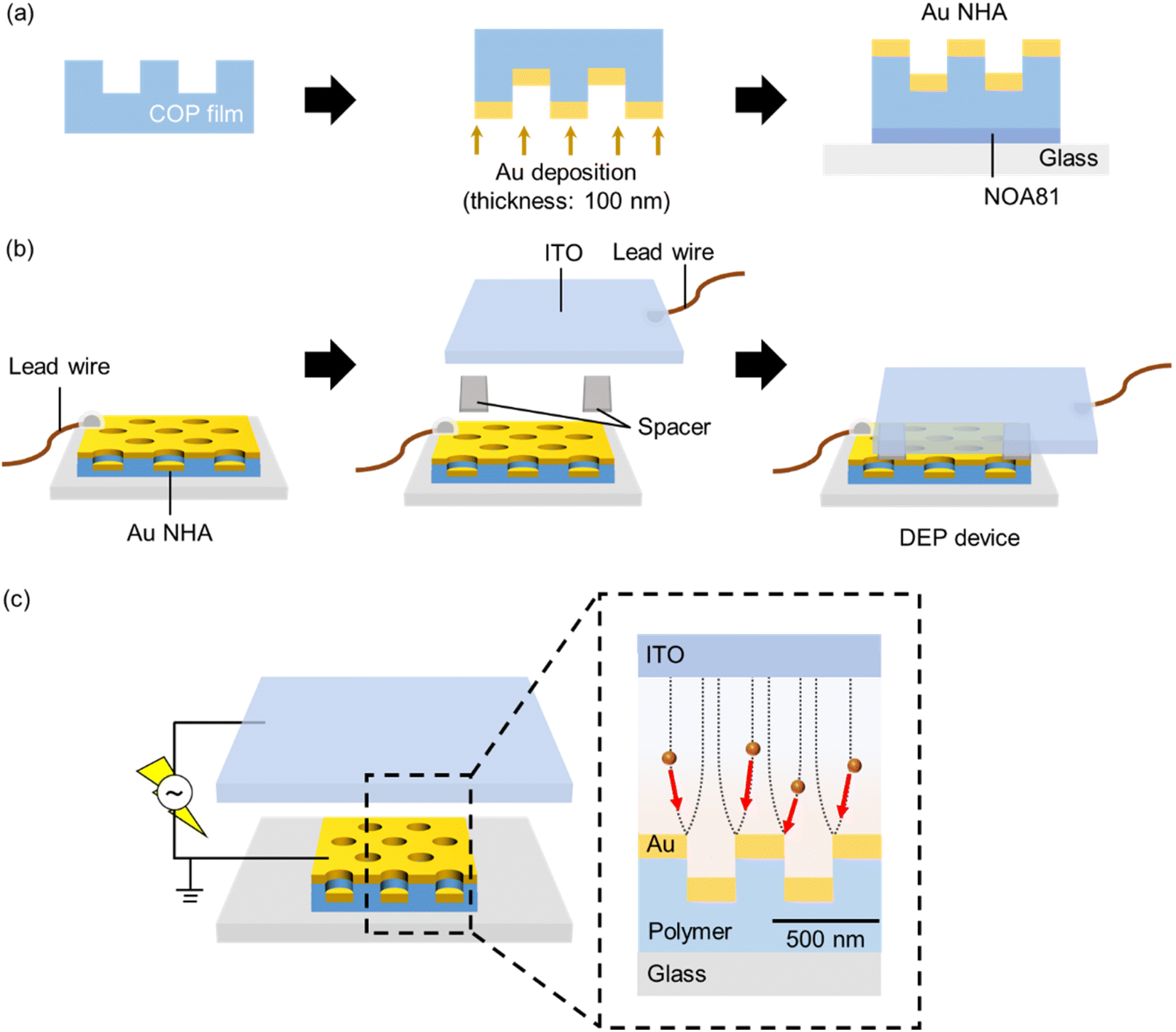 | ||
| Fig. 1 Schematic of the fabrication procedure of (a) Au NHA and (b) DEP device. (c) Schematic of the DEP experimental setup used in this study. | ||
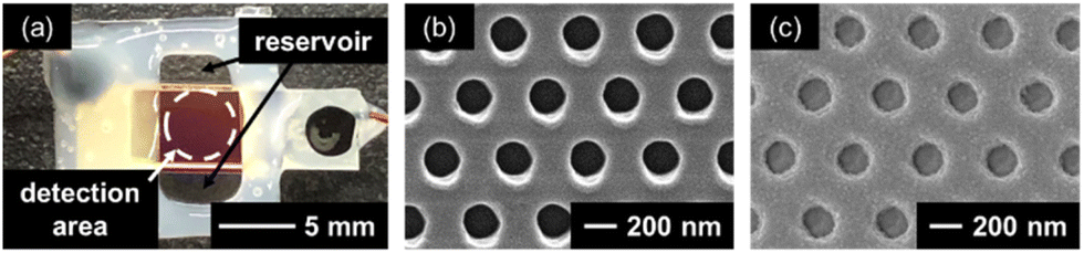 | ||
| Fig. 2 Images of (a) the fabricated Au NHA-based DEP device, (b) nanohole-imprinted COP film, and (c) fabricated Au NHA observed using a field-emission scanning electron microscope. | ||
2.2. Structural observation
The nanohole-imprinted COP film and Au NHA structures were observed using a field-emission scanning electron microscope (FE-SEM) (SU8010, Hitachi, Ibaraki, Japan) at an acceleration voltage of 10 keV, and an atomic force microscopy (AFM) (AFM5000II, Hitachi, Tokyo, Japan) in tapping mode using a silicon tip cantilever (SI-DF20) with a nominal spring constant of 15 N m−1.2.3. Optical characterization
Microspectroscopy was performed using an optical microscope (BX-53, Olympus Corp., Tokyo, Japan) to measure all optical spectra. The setup consisted of a tungsten–halogen white light source (380–780 nm), an Au NHA-based DEP device, an objective lens (OL) (magnification: ×10, numerical aperture: 0.30), an optical fiber probe (R400-7, UV-VIS, Ocean Optics, Tokyo, Japan), a handheld spectrophotometer (USB4000, Ocean Insight), and a software program (Ocean View, Ocean Insight), as shown in Fig. S1a.† The transmission spectra and normalized intensity (T) of the Au NHA, which were calculated using the transmission intensity of the white light source as a reference, were obtained using this optical setup. Thereafter, the subtracted spectrum (1 − T) was obtained. The responsivity to the refractive index (RI) was also evaluated using the same setup. Ultrapure water, ethanol, and 2-propanol (RI = 1.3332, 1.3594, and 1.3752, respectively) were added to the DEP device in sequence. Optical measurements were performed in triplicate using three independent Au NHAs (N = 3). The finite-difference time-domain (FDTD) method (ANSYS Inc., Vancouver, Canada) was used for the optical simulations (Fig. S1b, c, and S2†).2.4. Dielectrophoretic manipulations
![[thin space (1/6-em)]](https://www.rsc.org/images/entities/char_2009.gif) 000g, time: 10 min, number of times: triplicate). Each PS NP dispersion having a different concentration was introduced into the DEP device from the reservoir and left in the detection area (Fig. 2a, volume: <1 μL). Subsequently, a sinusoidal signal (1 kHz, 10 Vp–p) was applied between the ITO and Au NHA using a function generator (FGX-2220, TEXIO Technol. Corp., Yokohama, Japan). During dielectrophoretic manipulations, the fluorescence images were obtained using a scientific complementary metal oxide semiconductor (sCMOS) camera (Dhyana400D, Visualix Co., Ltd., Hyogo, Japan) and an optical microscope (BX-53, OL magnification: ×20, numerical aperture: 0.30), and the transmission spectra were measured using the same setup described in Section 2.3 (Fig. S1†).
000g, time: 10 min, number of times: triplicate). Each PS NP dispersion having a different concentration was introduced into the DEP device from the reservoir and left in the detection area (Fig. 2a, volume: <1 μL). Subsequently, a sinusoidal signal (1 kHz, 10 Vp–p) was applied between the ITO and Au NHA using a function generator (FGX-2220, TEXIO Technol. Corp., Yokohama, Japan). During dielectrophoretic manipulations, the fluorescence images were obtained using a scientific complementary metal oxide semiconductor (sCMOS) camera (Dhyana400D, Visualix Co., Ltd., Hyogo, Japan) and an optical microscope (BX-53, OL magnification: ×20, numerical aperture: 0.30), and the transmission spectra were measured using the same setup described in Section 2.3 (Fig. S1†).3. Results and discussion
3.1. Evaluation of the fabricated Au NHA-based DEP devices
A typical example of the fabricated Au NHA-based DEP device is shown in Fig. 2a. A specific red color resulting from the SP can be visually observed with the naked eye, confirming the successful fabrication of the device. The structures of the nanohole-imprinted COP film and fabricated Au NHA obtained by FE-SEM are shown in Fig. 2b and c, respectively. The diameters of the COP film and the fabricated Au NHA were 225.3 ± 4.5 and 222.3 ± 4.6 nm, respectively. The corresponding lattice constants were 461.0 ± 2.6 and 459.2 ± 2.9 nm, respectively. Also, Fig. S4† showed that the Au layers deposited via direct deposition inside the nanohole and on the nanohole surface is almost same thickness. These results show that the Au NHA, which exhibited a similar shape to the nanohole-imprinted COP film, was simply obtained via the direct Au deposition method.The absorption spectra of the fabricated Au NHA in the DEP device for different RI solutions and FDTD simulations are shown in Fig. 3a. The simulated model was constructed based on the SEM image shown in Fig. 2c. When surrounded by water (RI = 1.3332), the fabricated Au NHA (Exp.) exhibited a maximum absorption peak at ∼581 nm. However, in the FDTD simulation (Sim.), the Au NHA demonstrated two absorption peaks at 561 and 592 nm and an absorption dip at 578 nm, which were related to the LSPR and SPP modes. In Fig. 3b, these peak and dip wavelengths were red-shifted as the RI increased and exhibited similar responsivity: 277.83 nm/RI (Exp.), 254.88 nm/RI (Sim., at 561 nm), 217.95/RI (Sim., at 578 nm) and 291.52 nm/RI (Sim., at 592 nm). In addition, two absorption peak wavelengths (561 and 592 nm) and a dip wavelength (578 nm) showed common EM fields at the edges of the nanoholes, and the spaces between the nanoholes below the Au layer in the simulation (Fig. 3c). These results suggest that the maximum absorption peak (581 nm) of the fabricated Au NHA was observed by merging the two peaks (561 and 592 nm) and the dip wavelength (578 nm) in the simulation. Also, the slight structure difference in the simulation and experiment may lead the spectra merging. These confirm that the maximum absorption peak (581 nm) observed in the fabricated Au NHA, where the EM field was at the edges of the nanoholes and in the spaces between the nanoholes, can be useful for detecting the RI and substances manipulated by DEP onto the surface of the Au NHA. In contrast, the wavelengths (776 and 788 nm) observed in the simulation may be related to the EOT modes from the EM fields (Fig. S2a†). These EOT modes have approximately twice higher responsivity to RI (532.12 nm/RI at 776 nm and 549.32 nm/RI at 788 nm) due to the stronger and wider EM fields at the edges of the nanoholes (Fig. S2a and b†); thus, they are more valuable. However, the simple optical setup used in this study does not allow the measurement and tracking of these EOT modes, as mentioned in Section 2.3 and subsequent sections. Furthermore, the Au disk at the bottom of the nanoholes may reduce the transmitted light intensity passing through the Au NHA, making it difficult to observe the transmitted light related to the EOT more precisely compared with the two peaks at 561 and 592 nm. The Au disk also plays a role in pushing the EM fields to the top of the Au surface,60 and therefore, the Au NHA with the Au disk may exhibit a higher sensitivity in the visible region than that without the Au disk. These estimations suggest that at the maximum absorption peak (∼581 nm), where the EM fields are similar to the EOT, it may be worth measuring the other SPP modes or LSPR as alternatives to the EOT.
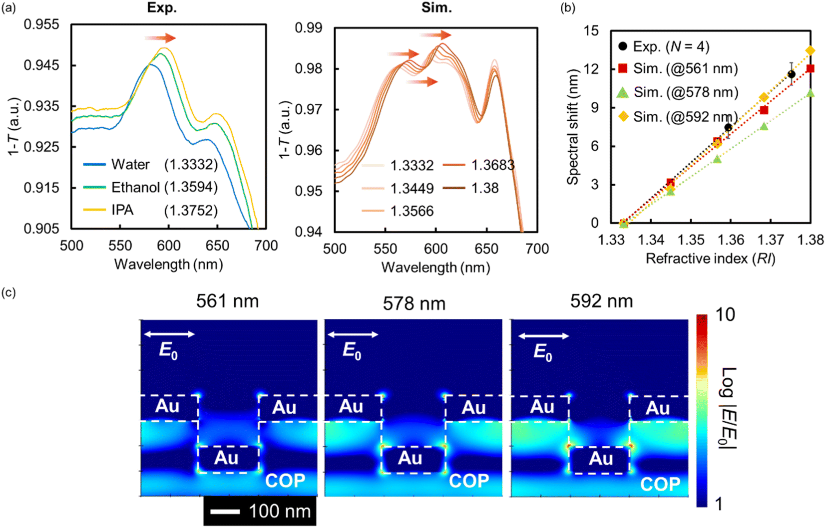 | ||
| Fig. 3 (a) Absorption spectra and (b) peak or dip shift with respect to the RI of the fabricated (Exp.) and simulated (Sim.) Au NHAs. (c) The EM fields of the two absorption peaks at 561 and 592 nm and a dip at 578 nm were obtained from the FDTD simulations. | ||
3.2. Dielectrophoretic manipulations of the fabricated Au NHA-based DEP devices
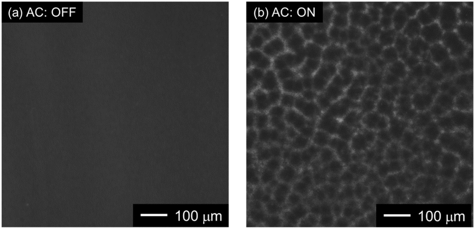 | ||
| Fig. 4 Fluorescence images (a) before and (b) after AC voltage was applied. | ||
As shown in Fig. 4b, a mesh pattern composed of many polygons (such as triangles, diamonds, and hexagons) was made by the trapped PS NPs. This indicates that the PS NPs were trapped onto the edges of the nanoholes, which had a triangular alignment.
The FEM simulations (Fig. 5) and SEM images (Fig. S6†) support this experimental result. As shown in Fig. 5, the edges of the nanoholes exhibited high ES field strength, while the spaces between the nanoholes exhibited moderate ES field strength. Fig. S6,† which shows the SEM images after drying the PS NP dispersion, also proves that the PS NPs were trapped onto both the edges of the nanoholes. These results experimentally and theoretically clarify the trapping spots by DEP. Furthermore, the locations of the EM fields at the maximum absorption peak wavelength of the Au NHAs were similar to the trapping spots simulated by the FDTD method and FEM (Fig. 3c and 5a). Therefore, changes in the maximum absorption peak of the fabricated Au NHAs can be used to properly evaluate the amount of substances trapped by DEP onto both the edges of the nanoholes.
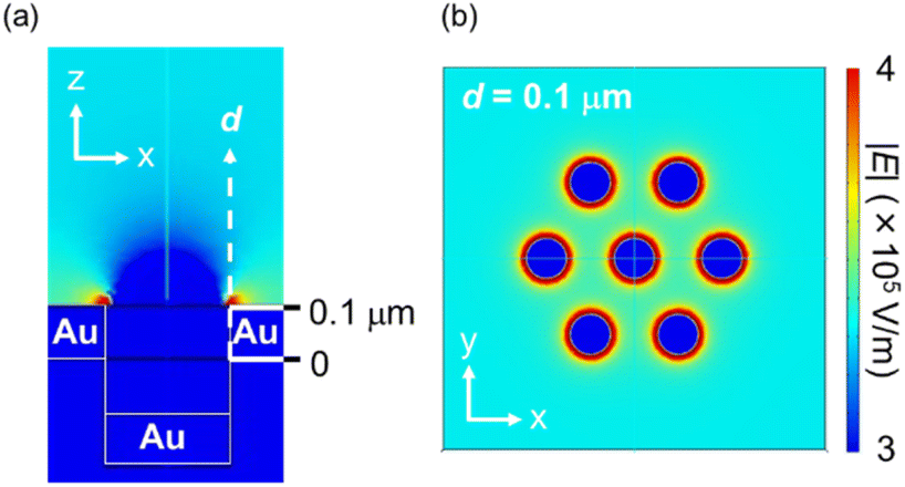 | ||
| Fig. 5 ES fields of the Au NHA obtained from FEM simulations: (a) x–z view and (b) x–y view at d = 0.1 μm when the AC condition was 1 kHz and 10 Vp–p. | ||
Following this, the amount of PS NPs trapped onto the Au NHAs via p-DEP and AC-EOF was quantitatively evaluated based on optical characterization. As shown in Fig. 6, the maximum peak of the Au NHAs rapidly red-shifted owing to PS NP trapping as soon as the AC voltage was applied, regardless of molecular diffusion. The change in the peak shift increased with an increase in the PS NP concentration as the RI on the Au NHA surface increased and reached saturation for ∼50 s for each PS NP concentration. These results strongly support those observed in the fluorescence and SEM images.
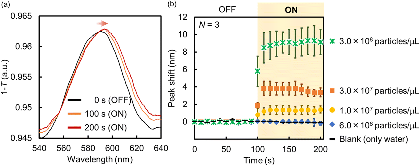 | ||
| Fig. 6 (a) Absorption spectra and (b) peak shift change of the Au NHAs before and after the application of AC voltage (samples: PS NP dispersions). | ||
Although the PS NPs could be trapped by DEP, the peak shift could not be changed when the PS NP concentration was less than 7.0 × 10⁶ particles per μL. This result is attributed to two limitations. The first one is the dielectrophoretic ability of the Au NHAs. In Fig. S3† and 5a, the strongest ES fields at the edges of the nanoholes extended only up to a height of 50 nm (d), even under AC-EOF conditions. This probably implies that the Au NHAs could only trap a significantly lesser amount of PS NPs compared with the amount of introduced PS NPs. The second limitation is the optical setup. In this study, the white light was illuminated from below the Au NHAs, and the transmission spectra were acquired using an OL and spectrophotometer. Therefore, it is not possible to use OLs with a high numerical aperture for low-light intensity detection due to the focal distance of the OLs. Moreover, the minimum resolution of the spectrophotometer was ∼0.3 nm. This was also reflected in the calculation of the limit of detection (LOD) (Fig. S7†).
In summary, the fabricated Au NHA-based DEP devices allow the simple, rapid, label-free trapping of PS NPs onto certain positions of the Au NHA as well as detection in the visible region. Thus, we expect that the Au NHA-based DEP devices can be used for the trapping and detection of various substances in solutions.
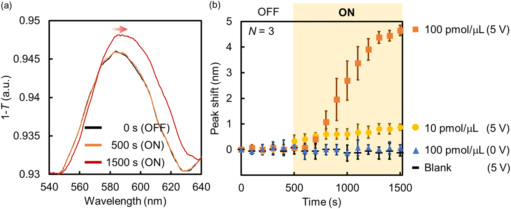 | ||
| Fig. 7 (a) Absorption spectra and (b) peak shift change of the Au NHAs before and after the application of AC voltage (samples: BSA solutions). | ||
In summary, the fabricated Au NHA-based DEP devices can enrich BSA from the solution via p-DEP and AC-EOF, and the BSA trapping and enrichment can be evaluated using the SPP modes and LSPR in the visible region. The DEP devices can also detect lower BSA concentrations compared with previous reports;63–65 however, the DEP devices cannot enough detect fewer BSA molecules compared with previous reports using nanohole arrays even though they can enrich some BSA molecules on the surface.44,45 This is likely because of the lower sensitivity of the DEP devices that use LSPR and SPP modes in the visible region compared with those that use EOT in the NIR or IR region. However, it is expected that nanohole sensing using SPP modes and (L)SPR, including those in this study, will have more diverse applications. Various materials (e.g., metal NPs, quantum dots, metal oxides or nitrides, and antimonene) can be used to adjust the plasmonic resonance, photoluminescence, and absorption for light harvesting or high-resolution imaging in the visible region.28,66–68 For example, we have shown that the incorporation of functional nanomaterials into nanohole polymers fabricated by nanoimprint lithography (NIL) allowed the adjustment and control of the plasmonic property.69 Also, the sensitivity will be much better improved by tuning of the structures of Au NHAs such as the length of hole diameters and lattice constant in the future. Furthermore, we expect that our Au NHA-based DEP devices can be transformed into more powerful platforms for single-biomolecule detection (e.g., digital bioimaging,28 surface-enhanced Raman scattering,70 and Raman imaging71) in the near future because some nanomaterials can be controlled and assembled at certain positions of the Au NHA from the solution by DEP, as presented in this study.
4. Conclusions
In this study, polymer-based Au NHAs were successfully fabricated using a simple process and combined with ITO electrodes to fabricate Au NHA-based DEP devices. The FDTD simulation and the experimental results confirmed that the maximum absorption peak of the Au NHA was in the visible region and there were EM fields at the edges of the nanoholes and the surfaces between the nanoholes, which were related to SPP modes and LSPR, and red-shifted by RI change. Furthermore, the FEM simulations showed that the ES fields of the Au NHA appeared at locations similar to those of the EM fields. The fluorescence and SEM images strongly support the results of the FEM simulations. The spatial spread of the narrow EM field at the edge of nanoholes emerged by LSPR and SPP is very similar to the ES field. The SEM images after DEP trapping also supported this fact strongly. In this study, for the first time, where PS NP/BSA was trapped by DEP could be demonstrated both experimentally and theoretically. The Au NHA-based DEP devices developed in this study achieved simple, label-free, rapid, cost-effective PS NP/BSA trapping and enrichment by overcoming molecular diffusion via p-DEP and AC-EOF. Also, performing detection in the visible light region could evaluate DEP while suppressing the effects of heat compared to NIR or IR regions as much as possible. The experimental results indicate that the Au NHA-based DEP devices can evaluate and trap various micro/nanosized (bio)molecules and/or particles in solution. Although the sensitivity of the Au NHAs was lower than those of other plasmonic nanohole arrays owing to the use of SPP modes and LSPR instead of the EOT, the SPP modes and LSPR in the visible region exhibit extensive possibilities compared with the EOT, and this is achieved by combining various available functional materials. Also, the sensitivity will be much better improved by tuning of the structures of Au NHAs such as the length of hole diameters and lattice constant in the future. Furthermore, DEP helps the Au NHAs to attain higher sensitivity and allows the advanced application of digital and Raman bioimaging, owing to the manipulation and positioning of nanomaterials. We believe that our Au-NHA-based DEP devices are facile, inexpensive, and useful tools for real-time biomarker manipulation and monitoring.Author contributions
S. Fujiwara conceptualized and planned this work, performed all the experiments and simulations (FDTD and FEM), and analyzed the data. S. Fujiwara, M. Hata, I. Onohara, M. Suzuki, and T. Yasukawa designed the experiments. M. Hata, I. Onohara, M. Suzuki, T. Yasukawa, and T. Endo contributed to the FEM simulations. D. Kawasaki and T. Endo contributed to the FDTD simulations and assembled the optical setup. S. Fujiwara wrote the original draft and D. Kawasaki, M. Suzuki, T. Yasukawa, K. Sueyoshi, H. Hisamoto, and T. Endo edited the draft to improve the manuscript. All authors contributed to the discussion of this study and reviewed the manuscript.Conflicts of interest
There are no conflicts to declare.Acknowledgements
We would like to thank Prof. Yasushi Takahashi from Osaka Metropolitan University for the use of the field-emission scanning electron microscope (FE-SEM) system. We also thank Nayuko Wada, a graduate student from Osaka Metropolitan University, for providing support for the DLS measurements. This work was supported by the Japan Society for the Promotion of Science (JSPS) KAKENHI (grant numbers: 22H03941, 22K18760, 22J14065 and 22KJ2615).References
- J. Homola, S. S. Yee and G. Gauglitz, Sens. Actuators, B, 1999, 54, 3–15 CrossRef CAS.
- J. Homola, Chem. Rev., 2008, 108, 462–493 CrossRef CAS PubMed.
- X. Fan, I. M. White, S. I. Shopova, H. Zhu, J. D. Suter and Y. Sun, Anal. Chim. Acta, 2008, 620, 8–26 CrossRef CAS PubMed.
- K. A. Peterlinz and R. Georgiadis, Langmuir, 1996, 12, 4731–4740 CrossRef CAS.
- U. Schroter and D. Heitmann, Phys. Rev. B: Condens. Matter Mater. Phys., 1999, 60, 4992–4999 CrossRef CAS.
- S. D. Mazumdara, M. Hartman, P. Kampfer and M. Keusgen, Biosens. Bioelectron., 2007, 22, 2040–2046 CrossRef PubMed.
- X. Du, Y. Li, Y.-L. Xia, S.-M. Ai, J. Liang, P. Sang, X.-L. Ji and S.-Q. Liu, Int. J. Mol. Sci., 2016, 17, 144 CrossRef PubMed.
- Y. Song, V. Madahar and J. Liao, Ann. Biomed. Eng., 2010, 39, 1224–1234 CrossRef PubMed.
- S. Cai, J. Yan, H. Xiong, Y. Liu, D. Peng and Z. Liu, Analyst, 2018, 143, 5317–5338 RSC.
- J. Ferreira, M. J. L. Santos, M. M. Rahman, A. G. Brolo, R. Gordon, D. Sinton and E. M. Girotto, J. Am. Chem. Soc., 2009, 131, 436–437 CrossRef CAS PubMed.
- T. Sannomiya, O. Scholder, K. Jefimovs, C. Hafner and A. B. Dahlin, Small, 2011, 7, 1653–1663 CrossRef CAS.
- J. Martinez-Perdiguero, A. Retolaza, D. Otaduy, A. Juarros and S. Merino, Sensors, 2013, 13, 13960–13968 CrossRef CAS PubMed.
- A. E. Cetin, D. Etezadi, B. C. Galarreta, M. P. Busson, Y. Eksioglu and H. Altug, ACS Photonics, 2015, 2, 1167–1174 CrossRef CAS.
- N. Asai, T. Shimizu, S. Shingubara and T. Ito, Sens. Actuators, B, 2018, 276, 534–539 CrossRef CAS.
- C. Escobedo, A. G. Brolo, R. Gordon and D. Sinton, Anal. Chem., 2010, 82, 10015–10020 CrossRef CAS PubMed.
- C. Escobedo, Y.-W. Chou, M. Rahman, X. Duan, R. Gordon, D. Sinton, A. G. Brolob and J. Ferreira, Analyst, 2013, 138, 1450–1458 RSC.
- H. Im, H. Shao, Y. I. Park, V. M. Peterson, C. M. Castro, R. Weissleder and H. Lee, Nat. Nanotechnol., 2014, 32, 490–494 CAS.
- M. Soler, A. Belushkin, A. Cavallini, C. Kebbi-Beghdadi, G. Greub and H. Altug, Biosens. Bioelectron., 2017, 94, 560–567 CrossRef CAS PubMed.
- X. Li, M. Soler, C. I. Özdemir, A. Belushkin, F. Yesilköy and H. Altug, Lab Chip, 2017, 17, 2208–2217 RSC.
- J. A. Jackman, A. R. Ferhan and N.-J. Cho, Chem. Soc. Rev., 2017, 46, 3615–3660 RSC.
- A. G. Brolo, E. Arctander, R. Gordon, B. Leathem and K. L. Kavanagh, Nano Lett., 2004, 4, 2015–2018 CrossRef CAS.
- A. G. Brolo, S. C. Kwok, M. G. Moffitt, R. Gordon, J. Riordon and K. L. Kavanag, J. Am. Chem. Soc., 2005, 127, 14936–14941 CrossRef CAS PubMed.
- M. Saboktakin, X. Ye, U. K. Chettiar, N. Engheta, C. B. Murray and C. R. Kagan, ACS Nano, 2013, 7, 7186–7192 CrossRef CAS PubMed.
- S. Jeon, S. Lee, K.-H. Han, H. Shin, K.-H. Kim, J.-H. Jeong and J.-J. Kim, Adv. Opt. Mater., 2018, 6, 1701349 CrossRef.
- A. E. Cetin and H. Altug, ACS Nano, 2012, 6, 9989–9995 CrossRef CAS PubMed.
- C. Escobedo, A. G. Brolo, R. Gordon and D. Sinton, Nano Lett., 2012, 12, 1592–1596 CrossRef CAS PubMed.
- L. Feuz, P. Jonsson, M. P. Jonsson and F. Hook, ACS Nano, 2010, 4, 2167–2177 CrossRef CAS.
- A. Belushkin, F. Yesilkoy and H. Altug, ACS Nano, 2018, 12, 4453–4461 CrossRef CAS PubMed.
- D. Conteduca, I. Barth, G. Pitruzzello, C. P. Reardon, E. R. Martins and T. F. Krauss, Nat. Commun., 2021, 12, 3293 CrossRef CAS PubMed.
- Y. Zhu and P. J. Reece, ACS Appl. Nano Mater., 2021, 4, 10657–10664 CrossRef CAS.
- B. Krause, M. T. Pham, H. M. Luong, T. D. Nguyen and T. B. Hoang, ACS Appl. Nano Mater., 2022, 5, 1185–1191 CrossRef CAS.
- R. Krishnan, B. D. Sullivan, R. L. Mifflin, S. C. Esener and M. J. Heller, Electrophoresis, 2008, 29, 1765–1774 CrossRef CAS PubMed.
- A. Sonnenberg, J. Y. Marciniak, R. Krishnan and M. J. Heller, Electrophoresis, 2012, 33, 2482–2490 CrossRef CAS PubMed.
- M. Oh, V. Jayasooriya, S. O. Woo, D. Nawarathna and Y. Choi, ACS Appl. Nano Mater., 2020, 3, 797–805 CrossRef CAS PubMed.
- E.-M. Laux, X. Knigge, F. F. Bier, C. Wenger and R. Hölzel, Small, 2016, 12, 1514–1520 CrossRef CAS PubMed.
- S. D. Ibsen, J. Wright, J. M. Lewis, S. Kim, S.-Y. Ko, J. Ong, S. Manouchehri, A. Vyas, J. Akers, C. C. Chen, B. S. Carter, S. C. Esener and M. J. Heller, ACS Nano, 2017, 11, 6641–6651 CrossRef CAS PubMed.
- L. Shi, D. Kuhnell, V. J. Borra, S. M. Langevin, T. Nakamura and L. Esfandiari, Lab Chip, 2019, 19, 3726–3734 RSC.
- W. Zhao, L. Zhang, Y. Ye, Y. Li, X. Luan, J. Liu, J. Cheng, Y. Zhao, M. Li and C. Huang, Analyst, 2021, 146, 5962–5972 RSC.
- S. H. Kim, T. Yamamoto, D. Fourmy and T. Fujii, Small, 2011, 7, 3239–3247 CrossRef CAS PubMed.
- K. Mogi, C. Shirataki, K. Kihara, H. Kuwahara, Y. Hongoh and T. Yamamoto, RSC Adv., 2016, 6, 113000–113006 RSC.
- I. Onohara, M. Suzuki, Y. Isozaki, K. Tsumoto, M. Tomita and T. Yasukawa, Anal. Sci., 2022, 38, 235–239 CrossRef CAS.
- M. Hata, M. Suzuki and T. Yasukawa, Biosens. Bioelectron., 2022, 209, 114250 CrossRef CAS PubMed.
- M. Suzuki, S. Kawai, C. F. Shee, R. Yamada, S. Uchida and T. Yasukawa, Lab Chip, 2023, 23, 692–701 RSC.
- A. Barik, L. M. Otto, D. Yoo, J. Jose, T. W. Johnson and S.-H. Oh, Nano Lett., 2014, 14, 2006–2012 CrossRef CAS.
- L. Tu, L. Huang and W. Wang, Biosens. Bioelectron., 2019, 127, 19–24 CrossRef CAS PubMed.
- C. Schäfer, D. P. Kern and M. Fleischer, Lab Chip, 2015, 15, 1066–1071 RSC.
- M. A. Zaman, P. Padhy, P. C. Hansen and L. Hesselink, Phys. Rev. A, 2017, 95, 023840 CrossRef.
- K. J. Freedman, C. R. Crick, P. Albella, A. Barik, A. P. Ivanov, S. A. Maier, S.-H. Oh and J. B. Edel, ACS Photonics, 2016, 3, 1036–1044 CrossRef CAS.
- E. Babaei, D. Wright and R. Gordon, Nano Lett., 2023, 23, 2877–2882 CrossRef CAS PubMed.
- L. Liu, K. Chen, N. Xiang and Z. Ni, Electrophoresis, 2019, 40, 873–889 CrossRef CAS PubMed.
- S. Tanaka, M. Tsutsui, H. Theodore, H. Yuhui, A. Arima, T. Tsuji, K. Doi, S. Kawano, M. Taniguchi and T. Kawai, Sci. Rep., 2016, 6, 31670 CrossRef CAS PubMed.
- X. Knigge, C. Wenger, F. F. Bier and R. Hölzel, J. Phys. D: Appl. Phys., 2018, 51, 065308 CrossRef.
- M. Chinappi, M. Yamaji, R. Kawano and F. Cecconi, ACS Nano, 2020, 14, 15816–15828 CrossRef CAS PubMed.
- J. Bravo-Abad, A. I. Fernández-Domínguez, F. García-Vidal and L. Martín-Moreno, Phys. Rev. Lett., 2007, 99, 203905 CrossRef CAS PubMed.
- D. Pacifici, H. J. Lezec, L. A. Sweatlock, R. J. Walters and H. A. Atwater, Opt. Express, 2008, 16, 9222–9238 CrossRef.
- F. Przybilla, C. Genet and T. W. Ebbesen, Opt. Express, 2012, 20, 4697–4709 CrossRef.
- J. P. Monteiro, L. B. Carneiro, M. M. Rahman, A. G. Brolo, M. J. L. Santos, J. Ferreira and E. M. Girotto, Sens. Actuators, B, 2013, 178, 366–370 CrossRef CAS.
- T. Ohno, C. Wadell, S. Inagaki, J. Shi, Y. Nakamura, S. Matsushita and T. Sannomiya, Opt. Express, 2016, 6, 1594–1603 CrossRef CAS.
- S. Fujiwara, D. Kawasaki, K. Sueyoshi, H. Hisamoto and T. Endo, Micromachines, 2022, 13, 1182 CrossRef.
- K. Nakamoto, R. Kurita, O. Niwa, T. Fujii and M. Nishida, Nanoscale, 2011, 3, 5067–5075 RSC.
- S.-H. Huang, S.-K. Wang, H. S. Khoo and F.-G. Tseng, Sens. Actuators, B, 2007, 125, 326–336 CrossRef CAS.
- N. Sasaki, T. Kitamori and H.-B. Kim, Electrophoresis, 2012, 33, 2668–2673 CrossRef CAS PubMed.
- T. Yamamoto and T. Fujii, Nanotechnology, 2007, 18, 495503 CrossRef PubMed.
- B. H. Lapizco-Encinas, S. Ozuna-Chacón and M. Rito-Palomares, J. Chromatogr. A, 2008, 1206, 45–51 CrossRef CAS PubMed.
- E.-M. Laux, X. Knigge, F. F. Bier, C. Wenger and R. Holzel, Electrophoresis, 2015, 36, 2094–2101 CrossRef CAS.
- T. Xue, W. Liang, Y. Li, Y. Sun, Y. Xiang, Y. Zhang, Z. Dai, Y. Duo, L. Wu, K. Qi, B. N. Shivananju, L. Zhang, X. Cui, H. Zhang and Q. Bao, Nat. Commun., 2019, 10, 28 CrossRef CAS.
- X. Wang, X. Ma, E. Shi, P. Lu, L. Dou, X. Zhang and H. Wang, Small, 2020, 16, 1906459 CrossRef CAS PubMed.
- Y. Yang, A. Dev, I. Sychugov, C. Hägglund and S.-L. Zhang, J. Phys. Chem. Lett., 2023, 14, 2339–2346 CrossRef CAS PubMed.
- D. Kawasaki, K. Maeno, H. Yamada, K. Sueyoshi, H. Hisamoto and T. Endo, Sens. Actuators, B, 2019, 299, 126932 CrossRef CAS.
- A. Barik, S. Cherukulappurath, N. J. Wittenberg, T. W. Johnson and S.-H. Oh, Anal. Chem., 2016, 88, 1704–1710 CrossRef CAS PubMed.
- C. T. Ertsgaard, N. J. Wittenberg, D. J. Klemme, A. Barik, W. Shih and S.-H. Oh, Nano Lett., 2018, 18, 5946–5953 CrossRef CAS PubMed.
Footnote |
| † Electronic supplementary information (ESI) available. See DOI: https://doi.org/10.1039/d3ra03245k |
| This journal is © The Royal Society of Chemistry 2023 |