
 Open Access Article
 This Open Access Article is licensed under a
 Creative Commons Attribution 3.0 Unported Licence
A new melilite-type rare-earth borate CdTbGaB2O7 and multicolor tunable emission in the CdTb1−xSmxGaB2O7 (0 ≤ x ≤ 0.2) phosphors†
Xuean Chen *a,
Jinyuan Zhanga,
Weiqiang Xiaob and
Xiaoyan Songa
*a,
Jinyuan Zhanga,
Weiqiang Xiaob and
Xiaoyan Songa
aFaculty of Materials and Manufacturing, Key Laboratory of Advanced Functional Materials, Ministry of Education of China, Beijing University of Technology, 100124 Beijing, China. E-mail: xueanchen@bjut.edu.cn
bBeijing Key Laboratory of Microstructure and Property of Solids, Beijing University of Technology, 100124 Beijing, China
First published on 1st June 2023
Abstract
A new mixed metal borate, CdTbGaB2O7, was successfully synthesized using the high-temperature solution method and its crystal structure was determined by single-crystal X-ray diffraction with the following unit-cell data: P![[4 with combining macron]](https://www.rsc.org/images/entities/char_0034_0304.gif) 21m, a = b = 7.3487(1) Å, c = 4.7247(1) Å, V = 255.150(9) Å3, and Z = 2. It belongs to a new member of the melilite family, which features a 3D framework consisting of alternately stacked [Ga(B2O7)]n5n− tetrahedral layers and (Cd2+/Tb3+) cationic layers that are interconnected via B(Ga)–O–(Cd/Tb) bridges. In addition, the solid solutions of CdTb1−xSmxGaB2O7 (0 ≤ x ≤ 0.2) were prepared via the solid-state reaction method. The combined techniques of XRD, SEM, IR/Raman, XPS and PLE/PL were employed to characterize the products. It was found that the CdTb1−xSmxGaB2O7 phosphors simultaneously showed green emission of Tb3+ at 545 nm and orange emission of Sm3+ at 603 nm under excitation at 370 nm. The emission color can be adjusted from green to orange-red by varying the Sm3+ doped content via an energy transfer mechanism. For CdTb0.995Sm0.005GaB2O7, a QY of 13.22% was obtained, and its emission intensity at 423 K was 94% of that at 303 K. These results show that the prepared materials can act as potential color-tunable phosphors for UV w-LEDs.
21m, a = b = 7.3487(1) Å, c = 4.7247(1) Å, V = 255.150(9) Å3, and Z = 2. It belongs to a new member of the melilite family, which features a 3D framework consisting of alternately stacked [Ga(B2O7)]n5n− tetrahedral layers and (Cd2+/Tb3+) cationic layers that are interconnected via B(Ga)–O–(Cd/Tb) bridges. In addition, the solid solutions of CdTb1−xSmxGaB2O7 (0 ≤ x ≤ 0.2) were prepared via the solid-state reaction method. The combined techniques of XRD, SEM, IR/Raman, XPS and PLE/PL were employed to characterize the products. It was found that the CdTb1−xSmxGaB2O7 phosphors simultaneously showed green emission of Tb3+ at 545 nm and orange emission of Sm3+ at 603 nm under excitation at 370 nm. The emission color can be adjusted from green to orange-red by varying the Sm3+ doped content via an energy transfer mechanism. For CdTb0.995Sm0.005GaB2O7, a QY of 13.22% was obtained, and its emission intensity at 423 K was 94% of that at 303 K. These results show that the prepared materials can act as potential color-tunable phosphors for UV w-LEDs.
1. Introduction
Melilites include a large class of natural and synthetic compounds, whose general formula is A2XZ2O7, where A cations (A = Na, Ca, Sr, Ba, Cd, Pb, Y, Ln) are sandwiched between XZ2O7 tetrahedral layers (X = Be, Mg, Co, Fe, Mn, Cu, Zn, Cd, Al, Ga; Z = Be, B, Al, Ga, Si, Ge).1 The melilite-like compounds have been extensively investigated in the past due to their crystal chemical properties and potential applications. For example, crystallographic studies indicated that the stability of the melilite structure depends strongly on the degree of the size misfit between the tetrahedral layers and the interlayer cations.2 As far as their application prospects are concerned, some Si (or Ge)-based melilites may act as potential microwave dielectric materials.3 Doped with Nd3+, crystals of the melilite family, e.g. Ca2Ga2SiO7, Ba2MgGe2O7 and Ba2ZnGe2O7, were successfully used in high-power lasers, both with Xe-flash lamp pumping and with laser-diode pumping.4–6The mineral okayamalite, Ca2SiB2O7, was first discovered by Giuli et al. in 2000, which is the only melilite borate known at early times.7 Subsequently, Barbier et al. conducted a systematic survey of several MO–Bi2O3 (and Ga2O3)–B2O3 systems and found three new diborate members of this family, including Bi2ZnB2O7, CaBiGaB2O7, and CdBiGaB2O7 (only unit-cell data were provided for the last borate).8 Among them, two Ga-containing compounds crystallize with the normal tetragonal melilite structure, whereas the Zn-containing phase adopts a unique orthorhombic superstructure of melilite. The attempted solid-state syntheses of the other melilites, such as Bi2MB2O7 (M = Be, Mg, Co), MBiGaB2O7 (M = Mg, Sr, Ba), CaBiMB2O7 (M = B, Al, In), and MBiZnB2O7 (M = Y, Nd, Yb), were unsuccessful. The preliminary measurements of second-harmonic generation (SHG) efficiencies (deff) on powder samples yielded values of 4.0 (Bi2ZnB2O7) and 1.6 (CaBiGaB2O7) relative to a KH2PO4 (KDP) standard. The larger efficiency of Bi2ZnB2O7 was ascribed to the presence of planar BO3 groups and a higher concentration of the heavy and polarizable Bi3+ cations in its crystal structure. Soon after, relatively large single crystals of Bi2ZnB2O7 were successfully grown from a high-temperature melt by the top-seeded method, which reveals that this borate is a promising candidate for nonlinear optical (NLO) materials.9 This Zn-containing melilite diborate is still of current interest due to its potential value as a host to prepare different kinds of luminescent materials. For instance, Tb3+, Sm3+, Eu3+ and Dy3+-doped Bi2ZnB2O7 phosphors were synthesized and their luminescent properties were investigated.10–12 When active laser medium (such as Er3+, Nd3+ or Pr3+ ions) are doped into this crystal structure, the obtained crystals may show both luminescence and NLO properties, which makes them very attractive for the new generation of laser frequency converters, the representative crystals including Bi2ZnOB2O6:Yb3+/Er3+, Bi2ZnOB2O6:Nd3+ and Bi2ZnOB2O6:Pr3+.13–15 In addition, not long ago, two new melilite-type borogermanates, Ca2GeB2O7 and Ca1.78Cd0.22GeB2O7, were also reported, among which Ca2GeB2O7 has a short UV cutoff edge (<200 nm), indicating its potential as an optical material in the UV or DUV region.16 The compounds mentioned above are the only borates with melilite structure reported so far. In contrast to many investigations on Bi2ZnB2O7, there are no studies of CaBiGaB2O7 and CdBiGaB2O7 as promising hosts for luminescence applications, and also, there are no reports on rare-earth analogues of these borates in the literature.
It is well known that Tb3+ ions usually generate green emission arising from the 5D4 → 7FJ (J = 6, 5, 4, 3) transitions, while Sm3+ ions emit orange-red light due to the 4G5/2 → 6HJ (J = 5/2, 7/2, 9/2, 11/2) transitions.17 In Tb3+/Sm3+ co-doped systems, terbium plays the role of a sensitizer, and samarium is an activator. The energy transfer from Tb3+ to Sm3+ occurs, which makes it possible to achieve the multicolor tunable luminescence from green to orange-red by simply adjusting the ratio of these two ions. With these materials, it will be more convenient to control the color output according to the practical application requirements. Therefore, the study of Tb3+/Sm3+ co-doped phosphors is not only of theoretical but also of practical significance, and some previously reported examples are KBaY(MoO4)3:Ln3+ (Ln3+ = Tb3+, Eu3+, Sm3+, Tb3+/Eu3+, Tb3+/Sm3+), CaLa2(MoO4)4![[thin space (1/6-em)]](https://www.rsc.org/images/entities/char_2009.gif) :Tb3+/Sm3+, and Ba3La(PO4)3:Tb3+/Sm3+.18–20
:Tb3+/Sm3+, and Ba3La(PO4)3:Tb3+/Sm3+.18–20
In the process of exploring new borate materials to study their structure–property relationships, we found that Bi3+ in CdBiGaB2O7 can be completely replaced by Tb3+, resulting in a new melilite diborate, CdTbGaB2O7. Insofar as we know, it represents the first quaternary compound within CdO–Ln2O3–Ga2O3–B2O3 (Ln = trivalent rare-earth cations) system, and it is also the only rare-earth borate of the melilite family known to date. In this work, we first performed the synthesis and characterization of CdTbGaB2O7, then introduced Sm3+ into CdTbGaB2O7 to prepare CdTb1−xSmxGaB2O7 solid solutions (x = 0–0.2), and further studied the luminescence properties and energy transfer of Sm3+ doped CdTbGaB2O7. The obtained results suggest that this type of novel phosphors could serve as a multi-color component in UV w-LEDs.
2. Experimental section
2.1. Materials and methods
All chemicals, including CdCO3 (A.R.), Tb4O7 (99.99%), Tb(NO3)3·6H2O (A.R.), Sm2O3 (99.99%), Ga2O3 (99.99%) and H3BO3 (A.R.), were commercially available from Sinopharm Chemical Reagent Co. Ltd and used without further purification. The XRD plots were recorded on a Bruker AXS D8 ADVANCE diffractometer equipped with Cu Kα1 radiation (λ = 1.5406 Å) operating at 40 kV and 40 mA. Surface morphology and element compositions of the synthetic product were characterized by a Hitachi SU8020 field emission scanning electron microscope (FE-SEM) equipped with an energy dispersive X-ray spectrometer (EDX). The Infrared (IR) spectra were measured with a Bruker VERTEX70 FT-IR spectrometer using the KBr pellet method. The Raman studies were carried out using a Renishaw InVia Raman spectrometer equipped with a confocal DM 2500 Leica optical microscope, a thermoelectrically cooled CCD as a detector, and He/Ne laser as an exciting source working at 633 nm. The X-ray photoelectron spectroscopy (XPS) measurements were done by a Thermo ESCALAB 250xi spectrometer equipped with Al Kα (hν = 1486.6 eV) as an excitation source. The UV-vis absorption spectra were monitored using a Hitachi UH4150 spectrophotometer equipped with an integrating sphere attachment. The excitation and emission spectra as well as decay kinetics were investigated using an Edinburgh FLS 1000 system equipped with a 450 W Xe lamp and a 60 W μF flash lamp. Quantum yield (QY) and temperature-dependent emission spectra were determined by the same spectrometer with a BaSO4-coated integrating sphere and a temperature controlling system, respectively.2.2. Synthetic procedures
Single crystals of CdTbGaB2O7 were grown by the high-temperature solution method. In a typical procedure, a powder mixture of 0.5464 g CdCO3, 0.1974g Tb4O7, 0.4950 g Ga2O3 and 0.2612 g H3BO3 (molar ratio 12:1:10:16) was thoroughly ground and placed in a Pt crucible. The mixture was slowly heated to 950 °C in a muffle furnace, and maintained at this temperature for 6 h to ensure that the raw materials are completely melted and uniformly mixed. Subsequently, the solution temperature was decreased, first to 700 °C at a rate of 1.5 °C h−1, then to 400 °C at 5.0 °C h−1, and finally to room temperature at 20 °C h−1. Many colorless, transparent, block-shaped crystals were obtained. Energy-dispersive X-ray analysis in a scanning electron microscope confirmed that the crystal contains the elements Cd, Tb, Ga, and O with an approximate atomic ratio of 10.44:8.25:6.65:74.66, which is close to its ideal composition of 1:1:1:7 (B is too light to be detected, see Fig. S1†).
The powder samples of CdTb1−xSmxGaB2O7 (x = 0, 0.001, 0.002, 0.005, 0.01, 0.05, 0.1, 0.2, and 1) were obtained through solid-state reactions of the calculated amounts of CdCO3, Tb(NO3)3·6H2O, Sm2O3, Ga2O3, and H3BO3. The well-ground samples were first preheated at 500 °C for 12 h and then sintered at 800 °C for 120 h with several intermediate re-mixings. Finally, the as-synthesized samples were ground into fine powder and their phase purity was checked by powder X-ray diffraction.
2.3. Single-crystal X-ray diffraction
Single-crystal diffraction data were collected at room temperature on an Agilent Super Nova diffractometer equipped with a Mo X-ray source (λ = 0.71073 Å). The data collection and reduction were performed with the CrysAlisPro software, and absorption corrections were made by the multi-scan method.21 The crystal structure was established by Direct Methods and subsequently refined by the full-matrix least-squares method on F2 on the basis of SHELX-2018.22 All atoms were refined anisotropically and the final difference Fourier synthesis did not reveal any significant residual peaks.Refinements of atomic occupancy parameters indicated that Cd and Tb atoms reside in the same atomic site (Wyckoff 4e) with the composition Cd0.5Tb0.5, which is not surprising since Cd2+ and Tb3+ have similar cationic radii (1.10 Å for Cd2+ vs. 1.04 Å for Tb3+, CN = 8) and coordination geometries.23 For this (Cd/Tb) site, no abnormally large displacement parameters were observed, and the largest principal anisotropic displacement parameter [U11 = U22 = 0.01079(11) Å2] was only about 1.3 times of the smallest one [U33 = 0.00832(13) Å2] (Table S2†). Therefore, it is not necessary to split (Cd/Tb) into two positions. In addition, the single-crystal XRD data did not show a symmetry lower than tetragonal or a larger unit cell that would allow the ordering of Cd2+/Tb3+. Finally, the disorder model was adopted. The flack parameter of this compound was refined to be −0.12(4). The program PLATON was used to check the positional parameters,24 and no higher symmetries were found. Details of unit-cell parameters, data collection and structure refinements are summarized in Table 1. Atomic coordinates and equivalent isotropic and anisotropic displacement parameters are given in Tables S1 and S2† and selected bond lengths and angles in Table S3.†
| Formula | CdTbGaB2O7 |
|---|---|
| a R1 = Σ||Fo| − |Fc||/Σ|Fo| and wR2 = [Σw(Fo2 − Fc2)2/ΣwFo4]1/2 for Fo2 > 2σ(Fo2). | |
| Formula weight | 474.66 |
| Space group | P21m (No. 113) |
| a (Å) | 7.3487(1) |
| c (Å) | 4.7247(1) |
| V (Å3) | 255.150(9) |
| Z | 2 |
| dcalc (g cm−3) | 6.178 |
| μ (mm−1) | 23.062 |
| 2θmax (°) | 69.94 |
| Unique reflections | 620 |
| Observed [I ≥ 2σ(I)] | 598 |
| No. of variables | 35 |
| GOF on Fo2 | 1.092 |
| R1/wR2 [I ≥ 2σ(I)] | 0.0221/0.0443 |
| R1/wR2 (all data) | 0.0236/0.0449 |
| Δρmax, Δρmin (e Å−3) | 1.528, −1.379 |
3. Results and discussion
3.1. Crystal structure description
CdTbGaB2O7 is a new member of the melilite series, and it is also the only rare-earth borate of this family known so far. In this structure, two BO4 tetrahedra first share a corner to form a diborate group, [B2O7]8−. Each [B2O7]8− dimer is linked to four different GaO4 tetrahedra, and, likewise, each GaO4 tetrahedron is connected to four neighboring [B2O7]8− groups via common O atoms to form a 2D infinite [Ga(B2O7)]n5n− layer extending in the (001) plane [see Fig. 1(b)]. These gallium borate anionic layers are stacked along the crystallographic c-axis direction, and (Cd2+/Tb3+) cations are placed in the square antiprismatic cavities between the layers to hold them together via (Cd/Tb)–O bonds, thus obtaining a 3D [CdTbGa(B2O7)]n framework [Fig. 1(a)].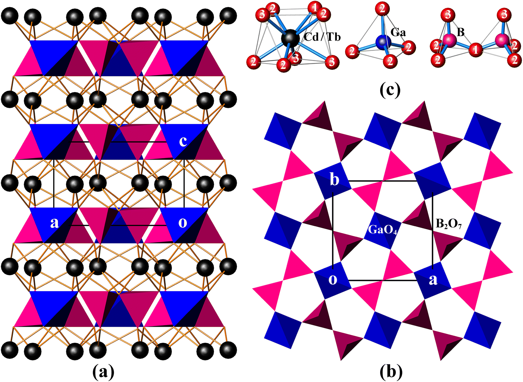 | ||
| Fig. 1 The unit cell of CdTbGaB2O7 projected along [010] (a), the [Ga(B2O7)]n5n− layer viewed along [001] (b), and the coordination environment of each cation site (the numbers correspond to the oxygen atom designations) (c). (Cd/Tb): black spheres; GaO4: blue tetrahedra; BO4: magenta tetrahedra. | ||
As shown in Table S1,† the asymmetric unit of CdTbGaB2O7 contains one disordered (Cd/Tb), one Ga, one B and three O sites. Among them, each (Cd/Tb) has eight O nearest-neighbors arranged into a distorted square antiprism [Fig. 1(c)]. The (Cd/Tb)–O distances fall in the range of 2.305(4)–2.547(3) Å, with an average of 2.430 Å (Table S3†), which lies between 2.42 and 2.48 Å computed from crystal radii sums of Tb3+ and O2− as well as Cd2+ and O2− for 8-fold coordination, respectively.23 These distances also correspond to those found in α-CdUO4, CdPd3O4 and Ba2CdTb2(BO3)4, where 8-coordinated Cd2+ or Tb3+ exist.25–27 Both Ga and B atoms adopt a tetrahedral coordination configuration. However, the Ga atom is located on the axis, thereby resulting in four equal Ga–O bond lengths of 1.824(3) Å and two groups of O–Ga–O bond angles of 107.90(10)° and 112.7(2)°, while the B atom lies on a mirror plane, giving three groups of B–O distances of 1.419(7), 1.492(7) and 1.525(5) Å and four groups of O–B–O angles of 114.6(5)°, 116.1(3)°, 102.6(3)° and 102.9(4)°. The average O–Ga–O and O–B–O angles are 109.5° and 109.15°, respectively, indicating that the GaO4 tetrahedron is rather regular, while the BO4 is somewhat deformed (Table S3†). Similar GaO4 and BO4 groups have already been identified in K2Ga2O(BO3)2 and In4O2B2O7, respectively.28,29 Furthermore, the calculated bond valence sums are 3.10 for Ga3+ and 2.92 for B3+, respectively, close to their expected values, indicating the validity of the structure.30
In the literature, several compounds with the chemical formula containing “B2O7” are known, which have various structure types from extended 2D layers to 3D frameworks. For example, all Bi2CaB2O7, Bi2SrB2O7 and Bi1.48Eu0.52Pb0.5Sr0.5B2O7 contain topologically identical 2D [A2MO(BO3)2] [A = Bi, (Bi/Eu); M = Ca, Sr, (Pb/Sr)] layers built of corner-sharing [BO3]3− triangles and [MO6]10− trigonal prisms with [A2O]4+ groups accommodated within six-membered rings. However, the Ca and Sr compounds take an acentric structure with space groups Pna21 and P63, respectively, while the (Pb/Sr) phase crystallizes in the centrosymmetric R![[3 with combining macron]](https://www.rsc.org/images/entities/char_0033_0304.gif) c group.31,32 BaAl2B2O7 also has a layered structure, but being built up from [BO3]3− triangles and [Al2O7]8− groups, and the latter consists of two corner-sharing AlO4 tetrahedra.33 Bi2ZnB2O7 contains both tetrahedral [B2O7]8− and triangular [B2O5]4− diborate groups, which are alternately arranged in the a and b directions, and further bridged by tetrahedral Zn2+ centers through sharing three O atoms of each ZnO4 tetrahedron to generate a 2D [Zn2O2(B2O7)(B2O5)]n12n− layer. These zinc borate anionic layers are held together by the octahedrally coordinated Bi3+ cations to create a 3D framework.8 This is different from the case of CdTbGaB2O7, where the 3D network is only composed of [B2O7]8− tetrahedral dimers, GaO4 tetrahedra, and 8-coordinated (Cd2+/Tb3+) cations, and each GaO4 corner-shares with four [B2O7]8− units. It is the differences in the fundamental building blocks and their connection modes that make these structures significantly different, which enriches the structural chemistry of borates.
c group.31,32 BaAl2B2O7 also has a layered structure, but being built up from [BO3]3− triangles and [Al2O7]8− groups, and the latter consists of two corner-sharing AlO4 tetrahedra.33 Bi2ZnB2O7 contains both tetrahedral [B2O7]8− and triangular [B2O5]4− diborate groups, which are alternately arranged in the a and b directions, and further bridged by tetrahedral Zn2+ centers through sharing three O atoms of each ZnO4 tetrahedron to generate a 2D [Zn2O2(B2O7)(B2O5)]n12n− layer. These zinc borate anionic layers are held together by the octahedrally coordinated Bi3+ cations to create a 3D framework.8 This is different from the case of CdTbGaB2O7, where the 3D network is only composed of [B2O7]8− tetrahedral dimers, GaO4 tetrahedra, and 8-coordinated (Cd2+/Tb3+) cations, and each GaO4 corner-shares with four [B2O7]8− units. It is the differences in the fundamental building blocks and their connection modes that make these structures significantly different, which enriches the structural chemistry of borates.
3.2. IR and Raman spectra
CdLnGaB2O7 (Ln = Tb, Sm) crystallizes in the tetragonal space group P21m (D2d3, No. 113), and its primitive cell comprises two B2O7 “pyro” units. A free B2O7 group is composed of two corner-shared BO4 tetrahedra, which can be described as two BO3 groups connected by a bent BOB bridge, as shown in Fig. 1(c). In analogy with pyrophosphate and pyrogermanate groups (P2O7 and Ge2O7),34–36 the 21 internal modes of the free B2O7 group with C2v symmetry can be subdivided into: A1 + B1 symmetric and A1 + A2 + B1 + B2 antisymmetric stretching modes of the BO3 groups [νs(BO3) and νas(BO3), respectively]; A1 symmetric and B1 antisymmetric stretching modes of the BOB bridge [νs(BOB) and νas(BOB), respectively]: A1 bending mode of the BOB bridge [δ(BOB)]; A2 + B2 rocking modes of the BO3 groups [ρ(BO3)]; and 3A1 + 2A2 + 3B1 + 2B2 O–B–O bending modes [δ(BO3)] (see the correlation diagram presented in Table S4†). In the crystal, these modes will give rise to 7A1 + 4A2 + 4B1 + 7B2 + 10E internal modes. Translational (T′) and librational (L) modes of free B2O7, i.e. A1 + B1 + B2 and A2 + B1 + B2, transform in crystal into A1 + B2 + 2E and A2 + B1 + 2E external modes, respectively. In addition, the disordered (Cd/Tb) atoms occupy the 4e Wyckoff positions of Cs symmetry and Ga atoms the 2a positions of S4 symmetry (Table S1†). These atoms contribute totally with 2A1 + A2 + 2B1 + 3B2 + 5E translational modes. By adding all these modes and subtracting three acoustic modes (B2 + E), the following optical vibrational modes of the crystal can be obtained: Γoptic = 10A1 + 6A2 + 7B1 + 10B2 + 18E, in which E modes are twofold degenerated and often observed as one frequency. Among these modes, B2 and E are both IR- and Raman-active, A1 and B1 are Raman-active only, and A2 is silent. This analysis shows that 63 modes in the Raman spectrum (10A1 + 7B1 + 10B2 + 18E) and 46 modes in the IR spectrum (10B2 + 18E) are expected to be observed, resulting in 45 Raman and 28 IR frequencies, respectively. Due to the large number of modes and the overlap of some modes, a precise assignment of the individual bands to specific vibrational modes is difficult, but a rough assignment of groups is possible for both IR and Raman spectra.
Fig. S2† shows the room-temperature IR and Raman spectra of the CdLnGaB2O7 (Ln = Tb, Sm) samples. Due to experimental limitations, IR characterization below 500 cm−1 is not possible. Two compounds exhibit similar spectral profiles, reflecting their isostructural features. The tentative band assignments are based on literature data,29,37–39 and the frequencies of the B2O7 group are assigned according to the characteristic vibrations of the BOB bridge and the terminal BO3 groups. The bands due to the antisymmetric BO3 terminal stretching vibrations of the B2O7 group [νas(BO3)] and the antisymmetric BOB bridge stretching modes [νas(BOB)] are observed in the high-frequency region of 1250–900 cm−1. The intensities of these bands are generally greater in infrared than in Raman spectra.38 The strong Raman bands at about 787 (795) cm− 1 are assigned to the symmetric stretching of the terminal BO3 groups [νs(BO3)], while in infrared spectra, these vibrations are clearly observed in the region of 800–840 cm−1. The IR bands near 704 (719) cm−1 can be attributed to the stretching vibrations of GaO4 tetrahedra,40,41 which matches with the peaks at 668 (676) cm−1 in the Raman spectra. The absorption bands at 600–300 cm−1 correspond to the δ(BOB) and δ(BO3) bending modes, and the bending vibrations of the GaO4 tetrahedra also appear in this area, making it difficult to assign the bands below 600 cm−1.39,42 Thus, the IR and Raman spectra confirm the presence of B2O7 tetrahedral dimers and four-coordinated Ga3+ ions, in accordance with the results obtained from the single-crystal XRD analyses.
3.3. UV-vis absorption spectra
Fig. S3† shows the UV-visible absorption spectra of CdLnGaB2O7 (Ln = Tb, Sm) (converted from diffuse reflectance data). The spectrum of the Tb compound shows a wide absorption band superimposed with several weak absorption peaks below 500 nm, which are mainly attributed to the inter-configurational 4f–5d transitions and intra-configurational 4f–4f transitions of the Tb3+ ions, i. e. 7F6 → 5L8 at 352 nm, 7F6 → 5L10 at 370 nm, 7F6 → 5D3 at 377 nm and 7F6 → 5D4 at 489 nm, respectively.43 For CdSmGaB2O7, there is a strong absorption band below 300 nm with maxima at about 224 nm, which is mainly ascribed to the ligand (O2−) to metal charge transfer (CT) transition. In the region between 300 and 500 nm, a series of sharp absorption peaks were observed at about 317, 346, 363, 377, 405, 418, 444, 465, 472, and 483 nm, which can be assigned to the 6H5/2 → 4F11/2, 6H5/2 → 3H7/2, 6H5/2 → 4F9/2, 6H5/2 → 4D5/2, 6H5/2 → 4K11/2, 6H5/2 → 4M19/2, 6H5/2 → 4G9/2 + 4I15/2, 6H5/2 → 4F5/2, 6H5/2 → 4I11/2, 6H5/2 → 4M15/2 transitions, respectively, as found in the PLE spectrum [Fig. 4(b)].44,45The optical band gap (Eg) can be estimated with the help of Tauc's relation:46
| αhν = A(hν − Eg)n |
3.4. Phase purity and morphology
In order to check the correctness of the single-crystal structure, additional Rietveld refinements of powder XRD data from CdTb1−xSmxGaB2O7 (x = 0 and 1) were carried out using TOPAS software.49 In the refining process, the single-crystal data of the Tb phase were employed as the initial model, a total of 51 parameters were refined, including 47 profile and 4 structure ones. The final refinement patterns are depicted in Fig. 2(a) and (b), where the low R-factors and the small differences between the measured and calculated data were obtained, indicating good fitting quality and high phase purity. Although the cell dimensions of CdTbGaB2O7 from Rietveld refinements [a = b = 7.3437(1) Å, c = 4.7201(1) Å, and V = 254.558(8) Å3] are somewhat smaller than the single-crystal data [Table 1], their relative deviations are less than 0.5%, revealing that the determined structure should be quite credible. | ||
| Fig. 2 (a and b) Rietveld refinements of the XRD files for CdTb1−xSmxGaB2O7 (x = 0 and 1). (c) XRD patterns of the CdTb1−xSmxGaB2O7 (0 ≤ x ≤ 1) phosphors. (d) The cell parameters (a, c, and V) obtained by Rietveld refinements against the Sm3+ concentration (x). | ||
Powder XRD patterns of the as-prepared CdTb1−xSmxGaB2O7 (0 ≤ x ≤ 1) samples are presented in Fig. 2(c). All experimental diagrams agree well with the simulated pattern of CdTbGaB2O7, indicating that doping of Sm3+ ions did not generate any distinct impurity or induce significant changes in the host structure. In addition, the enlargement of the reflections in the range of 2θ = 32.8°–33.4° is shown in the right part of Fig. 2(c), where a continuous left-shift of the representative peak (121) can be clearly observed with increasing Sm3+ content in CdTb1−xSmxGaB2O7. In fact, as we discussed earlier, Cd and Tb atoms in CdTbGaB2O7 are statistically distributed over one atomic site, and each (Cd/Tb) is surrounded by eight oxygen atoms, forming a distorted (Cd/Tb)O8 polyhedron, while Ga and B atoms are completely ordered and tetrahedrally coordinated with oxygen atoms. Considering the ionic radii and coordination number (CN) of Cd2+ (1.10 Å, CN = 8), Tb3+ (1.040 Å, CN = 8), Sm3+ (1.079 Å, CN = 8), Ga3+ (0.47 Å, CN = 4) and B3+ (0.11 Å, CN = 4),23 it is reasonable to believe that the doped Sm3+ ions will replace Tb3+ and occupy (Cd/Tb) sites randomly in the host, which will lead to lattice expansion, thus shifting the diffraction peaks to smaller 2θ values according to the Bragg equation.
The ionic radii for eightfold coordinated Tb3+ and Sm3+ differ only by 3.75% and both fully concentrated Tb3+ and Sm3+ compounds are isostructural. Therefore, it is expected that there is a solid solution series whose lattice constants are linearly related to the Sm3+/Tb3+ ratio. In order to confirm this point, Rietveld refinements of powder XRD profiles were also performed on CdTb1−xSmxGaB2O7 (x = 0.001, 0.002, 0.005, 0.01, 0.05, 0.1 and 0.2), as shown in Fig. S4.† For these refinements, the atomic coordinates of Ga, B and O sites, atomic occupancies, and isotropic thermal displacement factors were fixed, while the atomic coordinates of the (Cd/Tb/Sm) site and cell parameters were refined along with other parameters. The lattice parameters and atomic coordinates of all species obtained from Rietveld fitting are summarized in Tables S5 and S6,† while the lattice parameters for 0 ≤ x ≤ 0.2 were plotted as a function of the dopant Sm3+ concentration (x) in Fig. 2(d). Obviously, cell parameters, including axis lengths (a and c) and volume (V), increase linearly with the incorporation of Sm3+, as predicted by Vegard law. This phenomenon can be explained by the larger ionic radius of Sm3+ compared to that of Tb3+, which is strong evidence of the successful cationic substitution.
The SEM images of the representative phosphor CdTb0.995Sm0.005GaB2O7 are illustrated in Fig. 3. The particles exhibit irregular shapes in the agglomerated form with several microns in size. They are typical products prepared by the high-temperature solid state reaction. Besides, the EDX spectrum reveals that in addition to Au as a coating element, there are expected elements in the studied sample, including Cd, Tb, Sm, Ga and O (B is too light to be detected). The elemental mappings demonstrate that all constituent elements are evenly distributed among the selected particle. Hence, the successful doping of Sm3+ into the CdTbGaB2O7 matrix to form a homogenous phase can be verified based on the XRD and EDX results.
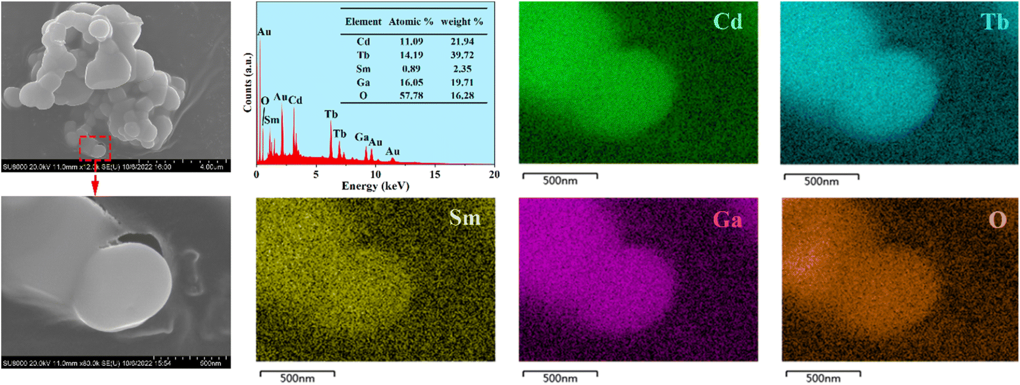 | ||
| Fig. 3 FE-SEM images, typical EDS results, and elemental mapping of the CdTb0.995Sm0.005GaB2O7 phosphor. Note that a thin layer of Au was evaporated on the sample surface to provide conductivity prior to SEM inspection. | ||
3.5. XPS spectra
XPS was performed to determine the surface chemical components of the phosphor CdTb0.995Sm0.005GaB2O7. Fig. S5(a)† depicts a typical survey scan in the range of 1350–0 eV, which contains Cd 3p, 3d, 4d, Tb 3d, 4d, Ga 2p, 3d, B 1s, O 1s and C 1s core levels along with Ga and O Auger peaks, confirming the sample composition. The presence of C can be ascribed to the expected adsorption of adventitious carbon from XPS instrument itself, and the C 1s peak of 284.6 eV was used as a standard to adjust other peaks. To further inspect the chemical state of each element, narrow scan XPS measurements were done, and the results are shown in Fig. S5(b)–(g).† One can see that there are two distinct peaks at 411.62 and 404.79 eV in Fig. S5(b),† which are assigned to Cd 3d3/2 and 3d5/2 core levels, and can be used as a fingerprint to identify the existence of Cd2+.50 The Tb 3d XPS spectrum is depicted in Fig. S5(c),† where two strong peaks associated with Tb 3d3/2 and 3d5/2 were clearly observed at 1278.71 and 1243.76 eV. These binding energies and their differences confirm the +3 valence state of Tb in the doped system.51 In Fig. S5(d),† although the Sm 4d XPS signal is relatively weak because of the very low dopant concentration in the phosphor, it can be deconvoluted into three components, corresponding to Sm 4d3/2 (∼134.29 eV), 4d5/2 (∼130.98 eV) and a satellite peak (127.87 eV), respectively, similar to the earlier results obtained for β-RbSm(MoO4)2.52 This indicates that the doped Sm element predominantly maintains the state of Sm3+ in the CdTbGaB2O7 matrix. Furthermore, the Ga 3p spectrum is composed of doublet components at 108.58 eV (Ga 3p1/2) and 104.96 eV (Ga 3p3/2) with the spin–orbit splitting of ∼3.62 eV, indicating that Ga appears as +3 valence.53 The B 1s spectrum was fitted to a single peak, which is attributed to the B atoms bonded to oxygen atoms (B–O) in borates, and its binding energy of 191.57 eV is in good accord with the literature report.54 The O 1s spectrum can be resolved into two components, of which the main peak at 530.95 eV usually denotes the presence of structural oxide (O2−), while the shoulder peak at 532.77 eV corresponds to the oxygen in adsorbed water (H2O) at the sample surface.55 No other impurity peaks have been identified from the XPS spectra, supporting the aforementioned XRD and EDX analyses. All these observations ensure the successful cationic substitution, after which a systematic investigation of the photoluminescence properties of the CdTb1−xSmxGaB2O7 phosphors was conducted.3.6. PLE and PL spectra
Fig. 4(a) shows the typical photoluminescence excitation (PLE) and emission (PL) spectra of the CdTbGaB2O7 phosphor. The PLE spectrum obtained by monitoring 545 nm emission (Tb3+: 5D4 → 7F5) consists of two strong broad bands below 300 nm, along with many sharp peaks in the higher wavelength region. The strong broadband centered at ∼248 and 286 nm can be attributed to the spin-allowed (7F6–7DJ) and spin-forbidden (7F6–9DJ) 4f8 → 4f75d1 inter-configurational Tb3+ transitions, respectively.56 The other excitation peaks appearing at 318, 343, 352, 370, 377, and 485 nm correspond to the parity- and spin-forbidden 4f–4f transitions of the Tb3+ ion, that is, from the 7F6 ground state to the excited states of 5D0, 5L6, 5L8, 5L10, 5D3, and 5D4 levels, as labelled in Fig. 4(a).43 The PL spectrum recorded under the excitation of 370 nm gives four sets of characteristic optical transitions of Tb3+, namely 5D4 → 7FJ (J = 6, 5, 4, and 3) at approximately 491, 545, 587 and 623 nm, respectively. The transition of 5D4 → 7F5 at ∼545 nm is the most prominent, which explains the strong green emission of CdTbGaB2O7. As expected, no emission coming from 5D3 level has been observed due to the fast cross relaxation processes [Tb3+ (5D3) + Tb3+ (7F6) → Tb3+ (5D4) + Tb3+ (7F0)] present in fully concentrated terbium materials.57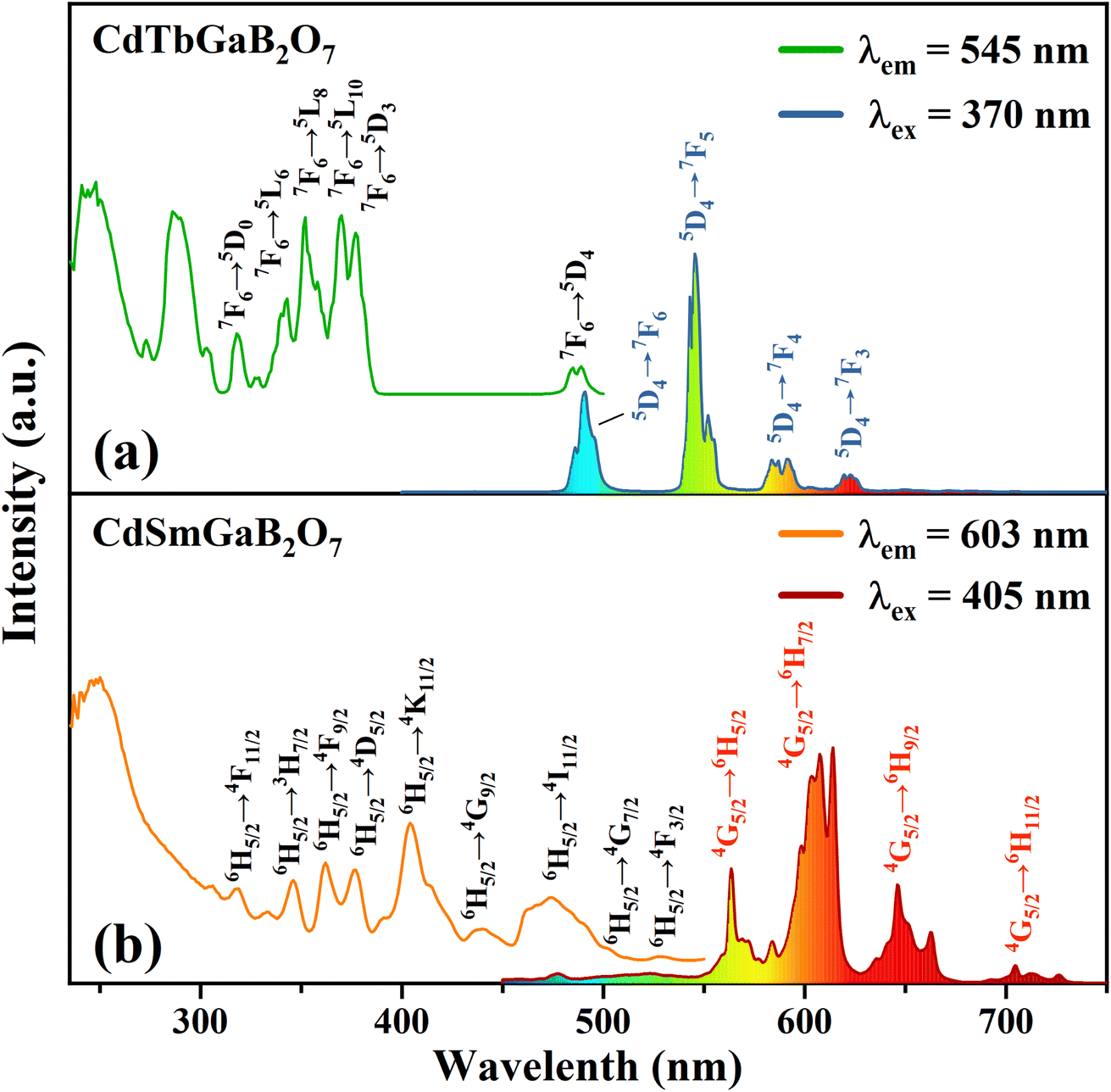 | ||
| Fig. 4 The PLE and PL spectra of CdTbGaB2O7 (a) and CdSmGaB2O7 (b). | ||
The PLE and PL spectra of the CdSmGaB2O7 phosphor are presented in Fig. 4(b). The PLE spectrum monitored with 603 nm emission exhibits a broadband near 250 nm together with multiple sharp peaks at 319, 346, 362, 377, 405, 440, 474, 502 and 528 nm, which are associated with the O2− → Sm3+ charge–transfer transition and the characteristic Sm3+ f–f transitions: 6H5/2 → 4F11/2, 6H5/2 → 3H7/2, 6H5/2 → 4F9/2, 6H5/2 → 4D5/2, 6H5/2 → 4K11/2, 6H5/2 → 4G9/2, 6H5/2 → 4I11/2, 6H5/2 → 4G7/2 and 6H5/2 → 4F3/2, respectively.44,45 The presence of the intense absorption bands from 350 to 490 nm suggests that CdSmGaB2O7 can be used as a potential phosphor for UV/NUV LED lighting. When the phosphor is exposed to 405 nm radiation, it emits luminescence at about 564, 603, 646, and 705 nm, assigned to the 4G5/2 → 6HJ (J = 5/2, 7/2, 9/2, 11/2) transitions of Sm3+, respectively. Among them, 4G5/2 → 6H5/2 and 4G5/2 → 6H9/2 are purely magnetic dipole (MD) and electric dipole (ED) allowed transitions, respectively, while 4G5/2 → 6H7/2 is a MD allowed one but also ED dominated. Generally speaking, the integral intensity ratio of the ED/MD transitions [R = I(4G5/2 → 6H9/2)/I(4G5/2 → 6H5/2)] is used to assess the symmetry nature of trivalent 4f ions. In this work, the R value was calculated as 1.45 (>1), implying that Sm3+ ions are located in the low symmetry sites. In fact, our structural analysis reveals that Sm3+ will replace Tb3+ and share the Wyckoff 4e site with Cd2+, which is on a mirror plane without inversion center, as shown in Table S1† and Fig. 1(c).
The PLE spectra of the CdTb1−xSmxGaB2O7 phosphors with different Sm3+ concentrations are shown in Fig. 5(a) and (b). By monitoring the Tb3+ emission at 545 nm (5D4 → 7F5), the PLE spectra show the f–d and f–f transitions of Tb3+ and the excitation intensity decreases remarkably and steadily towards a higher Sm3+ content and finally becomes negligible at x = 0.2, suggesting the presence of efficient Tb3+ → Sm3+ energy transfer. It is noteworthy that Sm3+ excitation peaks were undetectable in each case, which ascertains the fact that there was no possibility of energy transfer from Sm3+ to Tb3+. On the other hand, the PLE spectra monitored with the 603 nm emission (Sm3+: 4G5/2 → 6H7/2) contain not only the characteristic excitation peak of Sm3+ at 405 nm, but also those of Tb3+ originated from f–d and f–f transitions, with the latter dominating the PLE spectra, which further confirms the efficient Tb3+ → Sm3+ energy transfer. Besides, the intensities of the Tb3+ excitation transitions (e.g., 7F6–5L10 at 370 nm) successively increase with increasing Sm3+ concentration up to x = 0.005 and then decrease, implying the occurrence of concentration quenching at x > 0.005.
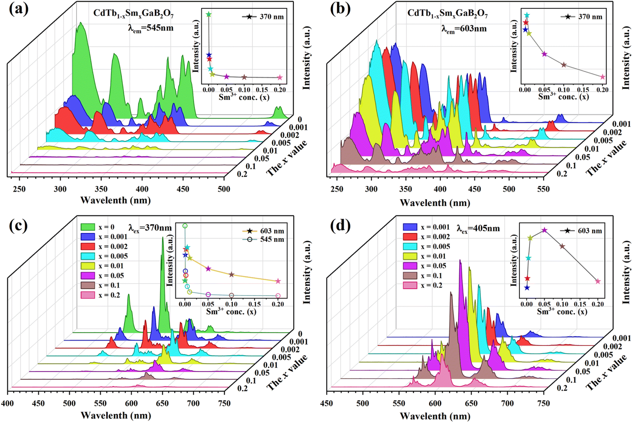 | ||
| Fig. 5 The concentration dependent PLE [(a) λem = 545 nm; (b) λem = 603 nm] and PL [(c) λex = 370 nm; (d) λex = 405 nm] spectra of the CdTb1−xSmxGaB2O7 fluorescent powders. | ||
The influence of Sm3+ content on the PL spectra of CdTb1−xSmxGaB2O7 were also studied, as shown in Fig. 5(c) and (d). As expected, upon excitation at 370 nm (Tb3+: 7F6 → 5L10), CdTbGaB2O7 displays only the characteristic emissions of Tb3+. With the doping of Sm3+ ions, besides Tb3+ emissions at 491 (5D4 → 7F6) and 545 nm (5D4 → 7F5), the characteristic emissions of Sm3+ at 603 nm (4G5/2 → 6H7/2) and 646 nm (4G5/2 → 6H9/2) can also be observed. Furthermore, as the Sm3+ concentration increases, the emission intensity of Tb3+ at 545 nm first decreases rapidly, and then remains at a relative low value with little difference, as illustrated in the inset of Fig. 5(c). At the same time, the emission intensity of Sm3+ at 603 nm increases initially until the Sm3+ concentration reaches x = 0.005, reflecting the result of energy transfer from Tb3+ to Sm3+. However, once the Sm3+ content is further increased to beyond x = 0.005, the concentration quenching occurs between Sm3+ ions, resulting in a decrease in the emission intensity. In addition, the PL spectra under direct excitation of the Sm3+ 4f levels at 405 nm (Sm3+: 6H5/2 → 4K11/2) yield only the emission peaks of Sm3+ and not those of Tb3+, further confirming the absence of energy transfer from Sm3+ to Tb3+. In this case, the emission intensity of Sm3+ first increases until x = 0.05 and then appears a downfall, which is consistent with the trend of Sm3+ characteristic excitation peak at 405 nm in the PLE spectra monitored at 603 nm emission of Sm3+ [Fig. 5(b)]. However, it is different from the situation observed in the 370 nm indirect excitation via the energy transfer from Tb3+ to Sm3+, where the optimal Sm3+ doped content is x = 0.005. As everyone knows, the PL spectrum is strongly affected by the excitation wavelength.58 The fact that indirect and direct excitation leads to different quenching concentrations has already been reported in some other phosphors, such as Ba3BiPbY1−xEuxO(BO3)4, CeO2:Eu3+ and SnO2:Eu3+.59–61
3.7. Fluorescence lifetime and energy transfer mechanism
To further illustrate the Tb3+ → Sm3+ energy transfer process, the Tb3+ luminescence decay curves of the CdTb1−xSmxGaB2O7 phosphors (λex = 370 nm, λem = 545 nm) were recorded, as shown in Fig. 6. All curves show a second-order exponential decay, which can be fitted by the following equation:where I0 and It are the luminescence intensities corresponding to time 0 and t, B1 and B2 are fitting parameters, and τ1 and τ2 are lifetimes for rapid and slow decays, respectively. The double-exponential behavior indicates a heterogeneous distribution of Tb3+ ions in the CdTb1−xSmxGaB2O7 phosphors. In fact, when the excitation energy is transferred from the donor (Tb3+) to acceptor (Sm3+), a double-exponential decay behavior of the activator is usually observed.17 The decay process is characterized by an average lifetime (τavg), which can be calculated as follows:

 | ||
| Fig. 6 Tb3+ decay curves of the CdTb1−xSmxGaB2O7 (0 ≤ x ≤ 0.2) phosphors monitoring 545 nm emission. | ||
The τavg values determined for different Sm3+ concentrations are also shown in Fig. 6. Apparently, the luminescence lifetime of Tb3+ in CdTb1−xSmxGaB2O7 decreases successively with the increase of Sm3+ concentration, which offers clear evidence for the energy transfer from Tb3+ to Sm3+. The energy transfer efficiency (η) from sensitizer to activator can be evaluated with the following expression:
| CdTb1−xSmxGaB2O7 | λex (nm) | CIE (x, y) | CCT (K) | η (%) |
|---|---|---|---|---|
| 1 x = 0 | 370 | (0.3134, 0.5750) | 5854 | — |
| 2 x = 0.001 | 370 | (0.4384, 0.4957) | 3574 | 52.85 |
| 3 x = 0.002 | 370 | (0.4656, 0.4779) | 3093 | 71.84 |
| 4 x = 0.005 | 370 | (0.5213, 0.4430) | 2227 | 82.44 |
| 5 x = 0.01 | 370 | (0.5539, 0.4202) | 1838 | 84.49 |
| 6 x = 0.05 | 370 | (0.5739, 0.4044) | 1677 | 86.39 |
| 7 x = 0.1 | 370 | (0.5746, 0.3979) | 1655 | 93.35 |
| 8 x = 0.2 | 370 | (0.5391, 0.3798) | 1706 | 96.20 |
Fig. 7 shows the energy level diagrams of Tb3+ and Sm3+ ions illustrating the energy migration processes in CdTb1−xSmxGaB2O7. Upon excitation at 370 nm, the electrons on Tb3+ ions can jump from the 7F6 ground state to the 5L10 excited state. Afterwards, the nonradiative transition (NR) took place, leading to the population of the 5D4 level. While some of the excited electrons return to the 7F6,5,4,3 ground state level in a radiative manner, generating the typical Tb3+ emissions. The remaining electrons at the 5D4 level of Tb3+ can move to the 4G7/2 excited level of Sm3+ due to energy level matching, followed by nonradiative relaxation to the 4G5/2 excited state and then radiative relaxation to the 6HJ (J = 5/2, 7/2, 9/2, 11/2) ground states to produce the observed Sm3+ emissions. This process enhances the characteristic emission of Sm3+ and simultaneously reduces the fluorescence emission intensity of Tb3+. In addition, it can be seen from Fig. 4(a) and (b) that there is a significant spectral overlap between the emission band of Tb3+ and the excitation band of Sm3+ in the range of 475–525 nm, which indicates that the energy transfer from Tb3+ to Sm3+ can be anticipated in CdTb1−xSmxGaB2O7 via 5D4 channel: 5D4 (Tb3+) + 6H5/2 (Sm3+) → 7F6 (Tb3+) + 4I11/2 (Sm3+).62 The Tb3+ → Sm3+ energy transfer is almost irreversible because the 5D4 level of Tb3+ is slightly higher than the 4G7/2 level of Sm3+, which also explains the observation that Tb3+ cannot be excited by 405 nm (Sm3+:6H5/2 → 4K11/2 transition) in this system.
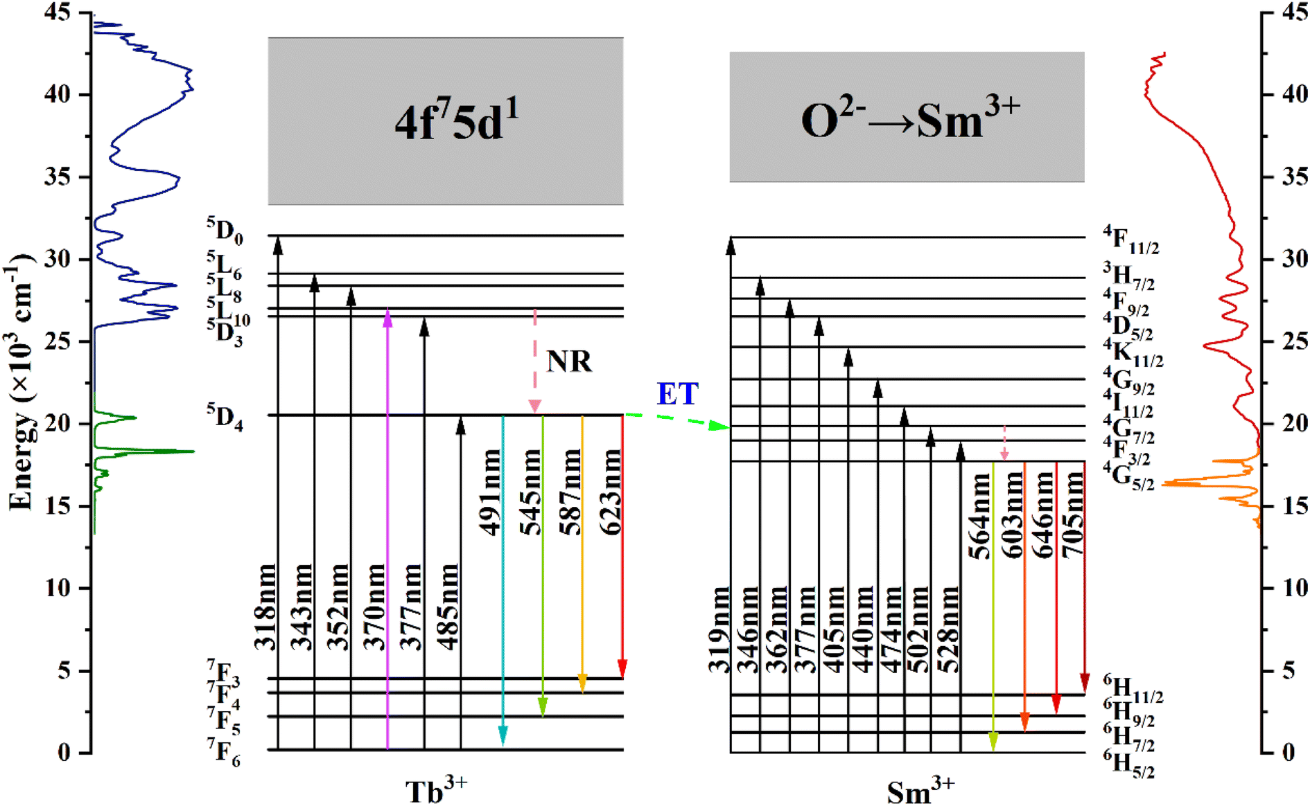 | ||
| Fig. 7 Schematic energy-level diagrams of Tb3+ and Sm3+ in CdTb1−xSmxGaB2O7, showing energy-transfer process (ET: energy transfer; NR: nonradiative). | ||
3.8. Emitting light color analysis
The CIE coordinates and CIE chromaticity diagram for the samples CdTb1−xSmxGaB2O7 (0 ≤ x ≤ 0.2) were measured, as shown in Table 2 and Fig. 8. The inset of Fig. 8 also shows the digital photos of the selected phosphors under a 370 nm UV lamp. One can see that the CdTbGaB2O7 host emits green light when excited at 370 nm. Once Sm3+ ions were doped into this host and the Sm3+ content changed from x = 0 to 0.1, the CIE coordinates of CdTb1−xSmxGaB2O7 would vary almost linearly from (0.3134, 0.5750) to (0.5746, 0.3979), which means that the emitting color changes continuously from green to orange-red. In addition, as seen from Fig. 5(c), when the Sm3+ content was further increased from x = 0.1 to 0.2, the characteristic blue and green emissions of Tb3+ remained basically unchanged, while the orange and red emissions of Sm3+ were significantly reduced due to the concentration quenching effect. Therefore, the chromaticity coordinates of the x = 0.2 sample are shifted toward the blue direction with respect to the x = 0.1 sample. A similar phenomenon was found in some previously reported Tb3+ and Sm3+ codoped phosphors, such as Y3Al2Ga3O12:0.5Tb3+, ySm3+, Na3Bi(PO4)2:0.1Tb3+, xSm3+ and LaAl2.03B4O10.54:0.1Tb3+, ySm3+.62–64 Next is the CCT (the Correlated Color Temperature), which is a measure of how cool or warm the appearance of a light source will be.65 The CCT can be calculated by the analytical equation proposed by McCamy:66| CCT = −449n3 + 3525n2 − 6823.3n + 5520.33 |
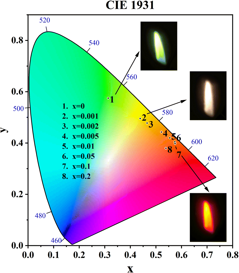 | ||
| Fig. 8 CIE chromaticity coordinates of the CdTb1−xSmxGaB2O7 (x = 0, 0.001, 0.002, 0.005, 0.01, 0.05, 0.1, 0.2) phosphors and digital photographs of the selected samples (x = 0, 0.001 and 0.1) (λex = 370 nm). | ||
3.9. Quantum yield and thermal stability
Quantum yield (QY) serves as a critical parameter to evaluate the luminescence properties of phosphors, which can be measured based on the following equation:where ∫LS is the integrated emission profile of the sample, ∫ER and ∫ES represent the integrated excitation profile without and with the sample in the integrating sphere, respectively. The excitation and emission spectra of the phosphor CdTb0.995Sm0.005GaB2O7 and the reference sample collected in an integrating sphere (λex = 370 nm) are displayed in Fig. S6,† which shows a QY of ∼13.22%. The relatively low QY may be due to the severe aggregation of phosphor particles. We believe that higher QY could be obtained by controlling the particle size, size distribution, morphology and crystalline defects via optimization of the preparation conditions or exploration of alternative synthetic routes. This will be investigated in our future work.

Thermal stability is one of the most important prerequisites for the synthesized phosphor to be used in a LED, as temperature greatly affects the brightness and color output. Fig. 9(a) exhibits the temperature-dependent PL spectra of the CdTb0.995Sm0.005GaB2O7 sample upon 370 nm excitation. Obviously, the position and shape of emission peaks remain almost unchanged, while the emission intensity diminishes with increasing temperature due to thermal quenching caused by non-radiative transitions. Furthermore, the emission intensities are integrated over the spectral range of 450–750 nm, and are normalized as compared to the case of 303 K. The results in the inset of Fig. 9(a) show that the relative emission intensity of CdTb0.995Sm0.005GaB2O7 at 423 K (the temperature at which LEDs typically operate) remains about 94% of that at 303 K. Compared with some previously reported phosphors, such as Ba3BiPbEuO(BO3)4 (37%), Ba2Lu4.48Eu0.5La0.02B5O17 (38.2%) and LaMgAl11O19:0.05Sm3+, 0.2Eu3+ (<60%),59,67,68 the thermal stability of CdTb0.995Sm0.005GaB2O7 seems to be better. For further understanding the influence of temperature on luminescence, the activation energy of thermal quenching (ΔE) was measured on the basis of the modified Arrhenius equation69:


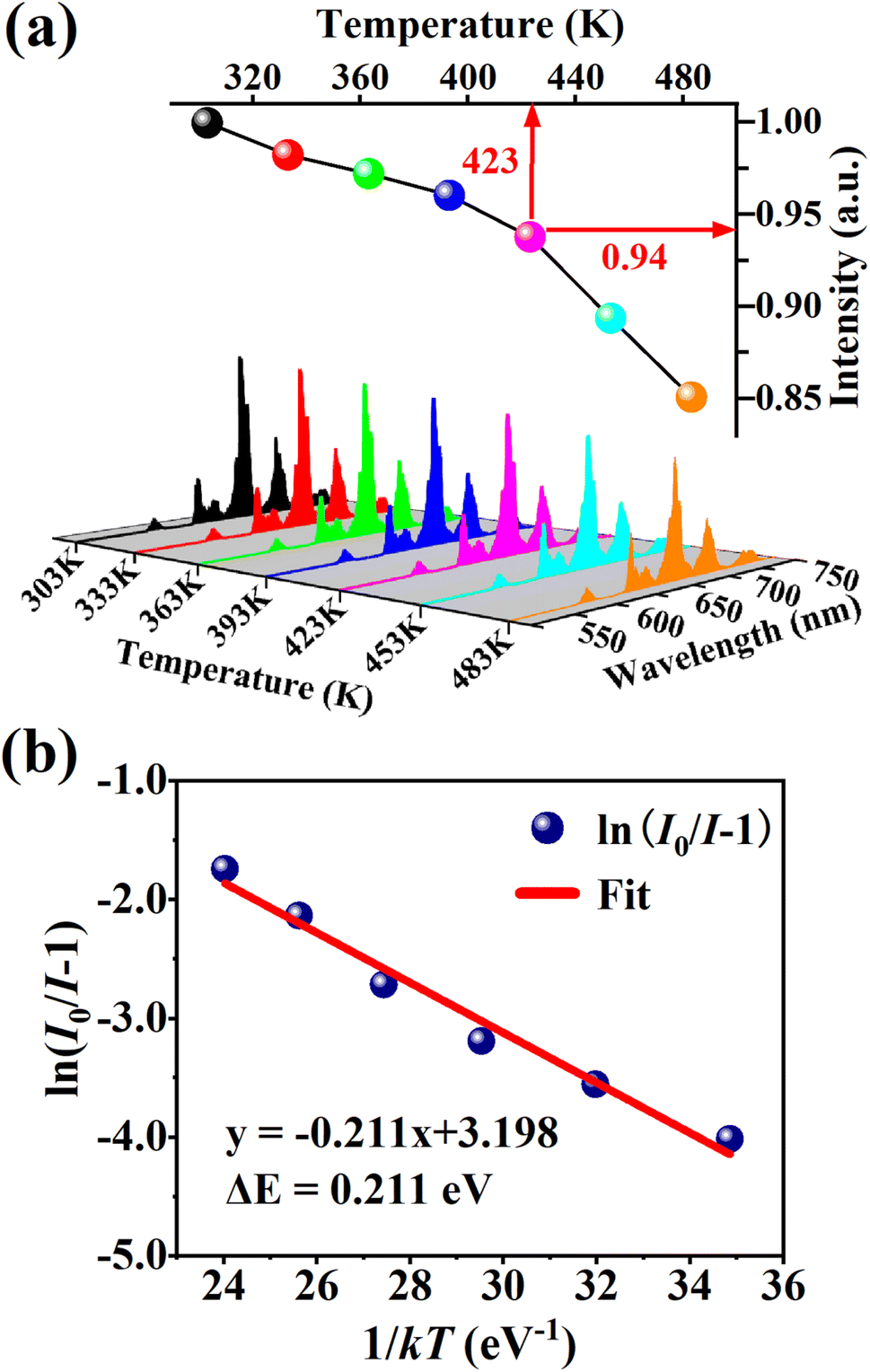 | ||
| Fig. 9 (a) PL spectra and normalized PL intensities of CdTb0.995Sm0.005GaB2O7 under different temperatures within 303–483 K (λex = 370 nm). (b) Relationship of ln(I0/I − 1) versus 1/kT for this phosphor. | ||
Fig. 9(b) shows the relationship between ln[(I0/I) − 1] and 1/kT of the phosphor. It can be seen that the plot can be well fitted to a straight line with the correlation coefficient R2 = 0.972 and the slope of −0.211, so the activation energy ΔE is 0.211 eV. The relatively high activation energy obtained in this work indicates that this phosphor possesses good color thermal stability and can be recommended as a suitable candidate for high-power LED applications.
4. Conclusions
CdTbGaB2O7 is the first quaternary compound found in the CdO–Ln2O3–Ga2O3–B2O3 (Ln = rare-earth metals) system. It has a melilite-type structure, in which [B2O7]8− tetrahedral dimers and [GaO4]5− tetrahedra share corners to generate 2D [Ga(B2O7)]n5n− layers that are further bridged by 8-coordinated (Cd2+/Tb3+) cations giving rise to a 3D framework. The IR and Raman studies supported the presence of B2O7 tetrahedral dimers and GaO4 groups. The UV-vis absorption measurement of CdTbGaB2O7 showed the typical Tb3+ absorption peaks and the band gaps of 4.10 and 4.33 eV for indirect and direct transitions, respectively. Furthermore, a series of CdTb1−xSmxGaB2O7 (0 ≤ x ≤ 0.2) phosphors was synthesized at 800 °C. Under the irradiation of 370 nm, the emission lines of Tb3+: 5D4 → 7F6,5,4,3 and Sm3+: 4G5/2 → 6H5/2,7/2,9/2,11/2 appeared simultaneously in the PL spectra of CdTb1−xSmxGaB2O7. The emission intensity of Tb3+ at 545 nm decreased monotonously, while that of Sm3+ at 603 nm first increased and then declined with increasing Sm3+ content, showing the Tb3+ → Eu3+ energy transfer and the concentration quenching between Sm3+ ions. The optimized CdTb0.995Sm0.005GaB2O7 phosphor exhibited a QY of 13.22% and good thermal stability with ΔE of 0.211 eV. The luminescence color can be tuned from green to orange-red by changing the Sm3+ doping concentration, and these types of materials have potential as tunable luminescence materials to meet the application requirements for n-UV LEDs.Conflicts of interest
There are no conflicts to declare.Acknowledgements
This work was supported by the National Key R&D Program of China (2021YFB3501502) and the National Natural Science Foundation of China (92163107).References
- L. P. Ogorodova, Y. D. Gritsenko, M. F. Vigasina, A. Y. Bychkov, D. A. Ksenofontov and L. V. Melchakova, Am. Mineral., 2018, 103, 1945–1952 CrossRef.
- F. Rothlisberger, F. Seifert and M. Czank, Eur. J. Mineral., 1990, 2, 585–594 CrossRef.
- C. Yin, Z. Yu, L. Shu, L. Liu, Y. Chen and C. Li, J. Adv. Ceram., 2021, 10, 108–119 CrossRef CAS.
- A. A. Kaminskii, H. R. Verdun and B. V. Mill, Phys. Status Solidi A, 1992, 129, K125–K130 CrossRef CAS.
- M. Alam, K. H. Gooen, B. Di Bartolo, A. Linz, E. Sharp, L. Gillespie and G. Janney, J. Appl. Phys., 1968, 39, 4728–4730 CrossRef CAS.
- D. J. Horowitz, L. F. Gillespie, J. E. Miller and E. J. Sharp, J. Appl. Phys., 1972, 43, 3527–3530 CrossRef CAS.
- G. Giuli, L. Bindi and P. Bonazzi, Am. Mineral., 2000, 85, 1512–1515 CrossRef CAS.
- J. Barbier, N. Penin and L. M. Cranswick, Chem. Mater., 2005, 17, 3130–3136 CrossRef CAS.
- N. Li, P. Fu, Y. Wu and J. Zhang, J. Cryst. Growth, 2009, 311, 3476–3478 CrossRef CAS.
- E. Erdoğmuş and E. Korkmaz, Optik, 2014, 125, 4098–4101 CrossRef.
- Q. Zhang, J. Wang, M. Zhang, W. Ding and Q. Su, J. Rare Earths, 2006, 24, 392–395 CrossRef.
- Q. Zhang, J. Wang, H. Ni and L. Wang, Rare Met., 2012, 31, 35–38 CrossRef CAS.
- D. Kasprowicz, K. Jaroszewski, P. Głuchowski, E. Michalski and A. Majchrowski, J. Alloys Compd., 2021, 873, 159772 CrossRef CAS.
- K. Jaroszewski, P. Gluchowski, M. G. Brik, T. Pedzinski, A. Majchrowski, M. Chrunik, E. Michalski and D. Kasprowicz, Cryst. Growth Des., 2017, 17, 3656–3664 CrossRef CAS.
- D. Kasprowicz, M. G. Brik, K. Jaroszewski, T. Pedzinski, B. Bursa, P. Głuchowski, A. Majchrowski and E. Michalski, Opt. Mater., 2015, 47, 428–434 CrossRef CAS.
- R. L. Tang, C. L. Hu, B. L. Wu, Y. Chen and J. G. Mao, Inorg. Chem. Front., 2019, 6, 2304–2310 RSC.
- K. P. Mani, G. Vimal, P. R. Biju, C. Joseph, N. V. Unnikrishnan and M. A. Ittyachen, Opt. Mater., 2015, 42, 237–244 CrossRef.
- K. Li and R. V. Deun, Dalton Trans., 2018, 47, 6995–7004 RSC.
- W. Xie, G. Liu, X. Dong, J. Wang and W. Yu, RSC Adv., 2015, 5, 77866–77872 RSC.
- W. Zhou, M. Gu, Y. Ou, C. Zhang, X. Zhang, L. Zhou and H. Liang, Inorg. Chem., 2017, 56(13), 7433–7442 CrossRef CAS PubMed.
- T. Skarzynski, M. Meyer and P. Stec, Acta Crystallogr., Sect. A: Found. Crystallogr., 2011, 67, C660–C661 Search PubMed.
- G. M. Sheldrick, Acta Crystallogr., Sect. C: Struct. Chem., 2015, 71, 3–8 Search PubMed.
- R. D. Shannon, Acta Crystallogr., Sect. A: Cryst. Phys., Diffr., Theor. Gen. Crystallogr., 1976, 32, 751–767 CrossRef.
- A. L. Spek, J. Appl. Crystallogr., 2003, 36, 7–13 CrossRef CAS.
- T. Yamashita, T. Fujino, N. Masaki and H. Tagawa, J. Solid State Chem., 1981, 37, 133–139 CrossRef CAS.
- O. Muller and R. Roy, Adv. Chem. Ser., 1971, 98, 28–38 CrossRef.
- R. R. Bian, X. A. Chen, W. Q. Xiao and X. Y. Song, J. Lumin., 2022, 242, 118545 CrossRef CAS.
- R. W. Smith, M. A. Kennard and M. J. Dudik, Mater. Res. Bull., 1997, 32, 649–656 CrossRef CAS.
- T. S. Ortner, D. Vitzthum, G. Heymann and H. Huppertz, Z. Anorg. Allg. Chem., 2017, 643, 2103–2109 CrossRef CAS.
- I. D. Brown and D. Altermatt, Acta Crystallogr., Sect. B: Struct. Sci., 1985, 41, 244–247 CrossRef.
- J. Barbier and L. M. D. Cranswick, J. Solid State Chem., 2006, 179, 3958–3964 CrossRef CAS.
- X. A. Chen, Y. An and W. Q. Xiao, J. Lumin., 2021, 237, 118137 CrossRef CAS.
- N. Ye, W. R. Zeng, B. C. Wu, X. Y. Huang and C. T. Chen, Z. Krist. - New Cryst. Struct., 1998, 213, 452 CAS.
- B. C. Cornilsen and R. A. Condrate sr, J. Phys. Chem. Solids, 1977, 38, 1327–1332 CrossRef CAS.
- J. Hanuza, M. Maczka, M. Ptak, J. Lorenc, K. Hermanowicz, P. Becker, L. Bohaty and A. A. Kaminskii, J. Raman Spectrosc., 2011, 42, 782–789 CrossRef CAS.
- S. N. Achary, D. Errandonea, D. Santamaria-Perez, O. Gomis, S. J. Patwe, F. J. Manjón, P. R. Hernandez, A. Muñoz and A. K. Tyagi, Inorg. Chem., 2015, 54(13), 6594–6605 CrossRef CAS PubMed.
- S. Filatov, Y. Shepelev, R. Bubnova, N. Sennova, A. V. Egorysheva and Y. F. Kargin, J. Solid State Chem., 2004, 177, 515–522 CrossRef CAS.
- V. V. Atuchin, A. K. Subanakov, A. S. Aleksandrovsky, B. G. Bazarov, J. G. Bazarova, T. A. Gavrilova, A. S. Krylov, M. S. Molokeev, A. S. Oreshonkov and S. Y. Stefanovich, Mater. Des., 2018, 140, 488–494 CrossRef CAS.
- J. Li, S. P. Xia and S. Y. Gao, Spectrochim. Acta, Part A, 1995, 51(4), 519–532 CrossRef.
- H. Fan, G. Wang and L. Hu, Solid State Sci., 2009, 11, 2065–2070 CrossRef CAS.
- G. Whichard and D. E. Day, J. Non-Cryst. Solids, 1984, 66, 477–487 CrossRef CAS.
- J. Ma, J. Chen, H. Xiang, J. Li, Y. Tang and L. Fang, Ceram. Int., 2022, 48, 6218–6224 CrossRef CAS.
- F. Baur, F. Glocker and T. Jüstel, J. Mater. Chem. C, 2015, 3, 2054–2064 RSC.
- X. Y. Chen, M. P. Jensen and G. K. Liu, J. Phys. Chem. B, 2005, 109, 13991–13999 CrossRef CAS PubMed.
- Y. C. Li, Y. H. Chang, Y. F. Lin, Y. S. Chang and Y. J. Lin, J. Alloys Compd., 2007, 439, 367–375 CrossRef CAS.
- J. Tauc, R. Grigorovici and A. Vancu, Phys. Status Solidi, 1966, 15, 627–637 CrossRef CAS.
- P. Y. Chen and G. Wang, Solid State Sci., 2020, 108, 106442 CrossRef CAS.
- P. Chen, M. M. Murshed and T. M. Gesing, J. Mater. Sci., 2021, 56, 3639–3652 CrossRef CAS.
- A. A. Coelho, J. Appl. Crystallogr., 2018, 51, 210–218 CrossRef CAS.
- Y. Purusothaman, N. R. Alluri, A. Chandrasekhar and S. J. Kim, J. Mater. Chem. C, 2017, 5, 415–426 RSC.
- N. X. Ca, N. D. Vinh, S. Bharti, P. M. Tan, N. T. Hien, V. X. Hoa, Y. Peng and P. V. Do, J. Alloys Compd., 2021, 883, 160764 CrossRef CAS.
- V. V. Atuchin, A. S. Aleksandrovsky, O. D. Chimitova, C. P. Diao, T. A. Gavrilova, V. G. Kesler, M. S. Molokeev, A. S. Krylov, B. G. Bazarov, J. G. Bazarova and Z. Lin, Dalton Trans., 2015, 44, 1805–1815 RSC.
- R. T. Haasch, E. Breckenfeld and L. W. Martin, Surf. Sci. Spectra, 2014, 21, 122–130 CrossRef CAS.
- V. V. Atuchin, S. V. Adichtchev, B. G. Bazarov, Zh. G. Bazarova, T. A. Gavrilova, V. G. Grossman, V. G. Kesler, G. S. Meng, Z. S. Lin and N. V. Surovtsev, Mater. Res. Bull., 2013, 48, 929–934 CrossRef CAS.
- S. Gu, W. Li, Y. Bian, F. Wang, H. Li and X. Liu, J. Phys. Chem. C, 2016, 120, 19242–19251 CrossRef CAS.
- X. Zhang and H. J. Seo, Mater. Res. Bull., 2012, 47, 2012–2015 CrossRef CAS.
- D. Qin and W. Tang, RSC Adv., 2017, 7, 2494–2502 RSC.
- Q. Cheng, Y. Dong, M. Kang and P. Zhang, J. Lumin., 2014, 156, 91–96 CrossRef CAS.
- X. A. Chen, R. R. Bian, W. Q. Xiao and X. Y. Song, Dalton Trans., 2022, 51, 9454–9466 RSC.
- X. Liu, S. Chen and X. Wang, J. Lumin., 2007, 127, 650–654 CrossRef CAS.
- J. Chen, J. Wang, F. Zhang, D. Yan, G. Zhang, R. Zhuo and P. Yan, J. Phys. D: Appl. Phys., 2008, 41, 105306 CrossRef.
- Z. Li, B. Zhong, Y. Cao, S. Zhang, Y. Lv, Z. Mu, Z. Hu and Y. Hu, J. Mater. Sci.: Mater. Electron., 2019, 30, 10491–10498 CrossRef CAS.
- Z. Zhu, G. Fu, Y. Yang, Z. Yang and P. Li, J. Mater. Sci., 2016, 51, 6944–6954 CrossRef CAS.
- Q. Ren, Y. Zhao, X. Wu and O. Hai, Polyhedron, 2020, 192, 114862 CrossRef CAS.
- R. Shrivastava, J. Kaur and V. Dubey, J. Fluoresc., 2016, 26, 105–111 CrossRef CAS PubMed.
- C. S. McCamy, Color Res. Appl., 1992, 17, 142–144 CrossRef.
- G. Annadurai, B. Devakumar, H. Guo, B. Li, L. Sun and X. Huang, RSC Adv., 2018, 8, 30396–30403 RSC.
- X. Min, Z. Huang, M. Fang, Y. G. Liu, C. Tang and X. Wu, Inorg. Chem., 2014, 53, 6060–6065 CrossRef CAS PubMed.
- F. Jensen, Qual. Reliab. Eng. Int., 1985, 1, 13–17 CrossRef.
Footnote |
| † Electronic supplementary information (ESI) available: The X-ray crystallographic file for CdTbGaB2O7 in CIF format; atomic coordinates, equivalent isotropic and anisotropic displacement parameters; selected bond distances and angles; correlation table of B2O7 between the site group of the molecule (C2ν) and the factor group of the crystal (D2d); Rietveld refinement results of CdTb1−xSmxGaB2O7 (0 ≤ x ≤ 1); the SEM image and EDX results of the CdTbGaB2O7 single-crystal; Rietveld refinements of powder X-ray diffractograms of CdTb1−xSmxGaB2O7 (0.001 ≤ x ≤ 0.2); IR, Raman, XPS and UV-vis absorption spectra; the excitation line of BaSO4 and the PL spectrum of the CdTb0.995Sm0.005GaB2O7 phosphor. CCDC 2253832. For ESI and crystallographic data in CIF or other electronic format see DOI: https://doi.org/10.1039/d3ra03002d |
| This journal is © The Royal Society of Chemistry 2023 |