
 Open Access Article
 This Open Access Article is licensed under a Creative Commons Attribution-Non Commercial 3.0 Unported Licence
Lead-free double perovskite Cs2MBiCl6 (M = Ag, Cu): insights into the optical, dielectric, and charge transfer properties
Mohamed Ben Bechir *a and
Mohamed Houcine Dhaoub
*a and
Mohamed Houcine Dhaoub
aLaboratory of Spectroscopic and Optical Characterization of Materials (LaSCOM), Faculty of Sciences, University of Sfax, BP1171 – 3000 Sfax, Tunisia. E-mail: mohamedbenbechir@hotmail.com
bDepartment of Physics, College of Science, Qassim University, P.O. Box: 6644, Almolaydah: 51452, Buraydah, Saudi Arabia
First published on 13th June 2023
Abstract
Recently, double perovskites have shown excellent potential considering the instability and toxicity problems of lead halide perovskites in optoelectronic devices. Here, the double perovskites Cs2MBiCl6 (M = Ag, Cu) were successfully synthesized via the slow evaporation solution growth technique. The cubic phase of these double perovskite materials was verified through the X-ray diffraction pattern. The investigation of Cs2CuBiCl6 and Cs2AgBiCl6 utilizing optical analysis showed that their respective indirect band-gap values were 1.31 and 2.92 eV, respectively. These materials, which are double perovskites, were examined using the impedance spectroscopy technique within the 10−1 to 106 Hz frequency and 300–400 K temperature ranges. Jonncher's power law was utilized to describe AC conductivity. The outcomes of the study on charge transportation in Cs2MBiCl6 (where M = Ag, Cu) suggest that the non-overlapping small polaron tunneling mechanism was present in Cs2CuBiCl6, whereas the overlapping large polaron tunneling mechanism was present in Cs2AgBiCl6.
1. Introduction
Thanks to their excellent optoelectronic properties, the well-known all-inorganic lead halides CsPbX3 (X = Br, Cl, and I) have been considered to be amongst the most potential optoelectronic materials.1–6 Different devices such as lasers, photodetectors, solar cells, and light-emitting diodes (LED)7–9 on the basis of lead-based perovskite compounds have been widely investigated. However, the toxic nature of lead and the instability of halide perovskite compounds under light conditions, high temperature, and moisture restrict the use of lead-halide perovskites in the future.10–12 Consequently, due to these problems, searching for non-toxic and stable lead-free perovskite candidates with good optoelectronic characteristics is among the most current research topics in the optoelectronics area.Current research has proved that the replacement of two divalent Pb2+ ions by a couple of trivalent and monovalent metal ions is a good way to resolve the stability and toxicity problems,13 in which the double perovskite compounds are developed with the well-known family A2MM′X6 (A = Rb+, Cs+, etc.; M = Ag+, K+, Li+; M′ = Sb3+, In3+ or Bi3+ and X = I−, Br− or Cl−).14,15 Especially, these families have drawn special consideration owing to their great moisture, thermal and light stability, and hence have been predicted as excellent replacements for lead-halide perovskites.14 Nevertheless, as compared to lead-halide perovskite, the majority of double perovskite materials show either the indirect bandgap with parity-forbidden transitions, which cause the weak photoluminescence behavior, or the wide indirect bandgap.15
Several investigations have focused on the synthesis and optical/optoelectronic studies of double perovskite materials,16 in which charge transport plays a significant role in the efficiency of electrical and optoelectronic devices. Nonetheless, a comprehensive comprehension of the electrical transport mechanism and dielectric properties of A2MM′X6 remains elusive.
The investigation of dielectric relaxation and AC conduction mechanisms across a broad range of temperatures and frequencies is typically conducted using dielectric spectroscopy.17 By analyzing multiple parameters such as AC conductivity, electrical modulus, dielectric permittivity, and complex impedance, the dielectric properties of a material can be studied, providing a qualitative representation that yields valuable insights. For example, the presence or absence of a relaxation peak in the imaginary modulus plots can indicate whether a material exhibits localized conduction (dielectric relaxation) or non-localized (long-range conductivity) processes. Furthermore, the relaxation time and activation energy for Cs2MBiCl6 (M = Ag, Cu) can be used to define specific transport mechanisms.18 The dielectric behavior has been studied in various materials such as conducting glasses, ionically conducting polymers, amorphous transition metal oxide semiconductors, and perovskite oxide materials.19
This paper presents the synthesis, optical, and structural characterizations of Cs2MBiCl6 (M = Ag, Cu). As these perovskites have not been extensively studied, this study provides a comprehensive investigation of their electrical and dielectric properties. To study the dielectric properties, impedance spectroscopy was used, which is a practical tool to analyze these properties. The dielectric study of the material as a function of frequency and temperature can provide detailed information on the conduction mechanism, loss factor, permittivity, and localized charge carriers. There is limited literature available on the research conducted on the AC conductivity and dielectric relaxation of Cs2MBiCl6 (M = Ag, Cu). In this work, the study of dielectric relaxation was conducted carefully as a function of temperature and frequency along with the conductivity of Cs2MBiCl6 (M = Ag, Cu), electrical modulus, and impedance spectroscopy. The results of the dielectric research were analyzed using various theoretical models. Additionally, detailed discussions on the dielectric constant, dielectric loss, AC and DC conductivity, as well as the electrical modulus and impedance study of these double perovskite materials are reported in this paper.
2. Experimental section
2.1. Materials
Silver chloride (Sigma-Aldrich, 99%), bismuth(III) chloride (Sigma-Aldrich, ≥98%), copper(I) chloride (Sigma-Aldrich, ≥99%), and cesium chloride (Sigma-Aldrich, ≥98%) were utilized without any additional purification treatment.2.2. Synthesis
The single crystals of Cs2MBiCl6 (M = Cu, Ag) were prepared using the slow solvent evaporation method as follows: a mixture of bismuth(III) chloride (0.839 g, 0.0026 mol/0.792 g, 0.0025 mol), cesium chloride (0.896 g, 0.0053 mol/0.846 g, 0.0050 mol), and copper(I)/silver chloride (0.263 g, 0.0026 mol/0.360 g, 0.0025 mol) was combined in 50 mL of deionized water at room temperature. Over several days, the solvent in the resulting solution, which contained the precursors for the double perovskite, gradually evaporated, resulting in the formation of single crystals of Cs2MBiCl6 (M = Cu, Ag). The utilization of the evaporation method offers numerous benefits, including advantages such as homogeneity and cost-effectiveness, among others.182.3. Characterization
To obtain fine powders for powder X-ray diffraction (PXRD) analysis, a small amount of Cs2MBiCl6 (M = Ag, Cu) crystals was ground using an agate mortar and pestle. PXRD analysis was conducted at room temperature using a Rigaku MiniFlex 600 benchtop diffractometer, with a Cu Kα line radiation (λ = 1.54 Å) in the 2θ range of 10–50° and a step size of 0.04°.A PerkinElmer Pyris 6 instrument was used to conduct thermogravimetric (TG) analysis on the powders obtained from Cs2MBiCl6 (M = Ag, Cu) crystals. The analysis was performed at different heating rates, from 0 to 1200 °C, in a closed perforated aluminum pan.
A PerkinElmer Lambda 950 UV-Vis spectrophotometer was used to measure the diffuse reflectance in the ultraviolet-visible region. The UV-Vis absorption spectrum was obtained at room temperature using a single crystal of Cs2MBiCl6 (M = Ag, Cu).
A small quantity of Cs2MBiCl6 (M = Ag, Cu) crystals was ground into fine powders using a pestle and agate mortar for complex impedance measurement. Pellets of Cs2MBiCl6 (M = Ag, Cu) with a thickness of approximately 1 mm were formed under a 50 Torr pressure and room temperature using an 8 mm hydraulic press. To ensure good electrical contact, silver paint was applied to the samples and they were placed between two copper electrodes. The AC conductivity and dielectric relaxation were measured using a TH2828A impedance analyzer at a frequency range of 10−1 to 106 Hz and a 2 K min−1 heating rate connected to a temperature controller (TP94, Linkam, Surrey, UK) at temperatures ranging from 300 to 400 K. The applied AC voltage was 0.5 V.
3. Results and discussion
The crystal structures of Cs2MBiCl6 (M = Ag, Cu) were obtained at ambient temperature through powder X-ray diffraction. Fig. 1(a) illustrates the diffractograms. Celeref3 software was used to index all reflection peaks via the least squares method utilizing the powder data. The PXRD analysis confirmed that Cs2MBiCl6 (M = Ag, Cu) adopted a cubic double perovskite structure with Fm![[3 with combining macron]](https://www.rsc.org/images/entities/char_0033_0304.gif) m space group symmetry. The unit cell parameters are a = 10.775 (8) Å and a = 10.364 (6) Å (α = β = γ = 90.00°) for Cs2AgBiCl6 and Cs2CuBiCl6, respectively. The parameters obtained for both compounds align with the information found in the bibliography.20,21 The photophysical properties of a material are intricately tied to its crystal structure. The literature suggests that double perovskites feature a three-dimensional arrangement of interconnected octahedra, where the cuboctahedral voids in the structure are filled with Cs+ ions.22 The structure of double perovskites is composed of octahedra centered on Cu+/Ag+ and Bi3+ ions, which alternate in all three directions, forming a superstructure commonly known as rock salt ordering. The crystal structure of Cs2MBiCl6 (M = Cu, Ag) exhibits a rock salt order structure, where alternating octahedral units of [BiCl6]3− and [MCl]5− are present. At the center of the cuboctahedra, there is a Cs+ ion, as depicted in Fig. 1(b).
m space group symmetry. The unit cell parameters are a = 10.775 (8) Å and a = 10.364 (6) Å (α = β = γ = 90.00°) for Cs2AgBiCl6 and Cs2CuBiCl6, respectively. The parameters obtained for both compounds align with the information found in the bibliography.20,21 The photophysical properties of a material are intricately tied to its crystal structure. The literature suggests that double perovskites feature a three-dimensional arrangement of interconnected octahedra, where the cuboctahedral voids in the structure are filled with Cs+ ions.22 The structure of double perovskites is composed of octahedra centered on Cu+/Ag+ and Bi3+ ions, which alternate in all three directions, forming a superstructure commonly known as rock salt ordering. The crystal structure of Cs2MBiCl6 (M = Cu, Ag) exhibits a rock salt order structure, where alternating octahedral units of [BiCl6]3− and [MCl]5− are present. At the center of the cuboctahedra, there is a Cs+ ion, as depicted in Fig. 1(b).
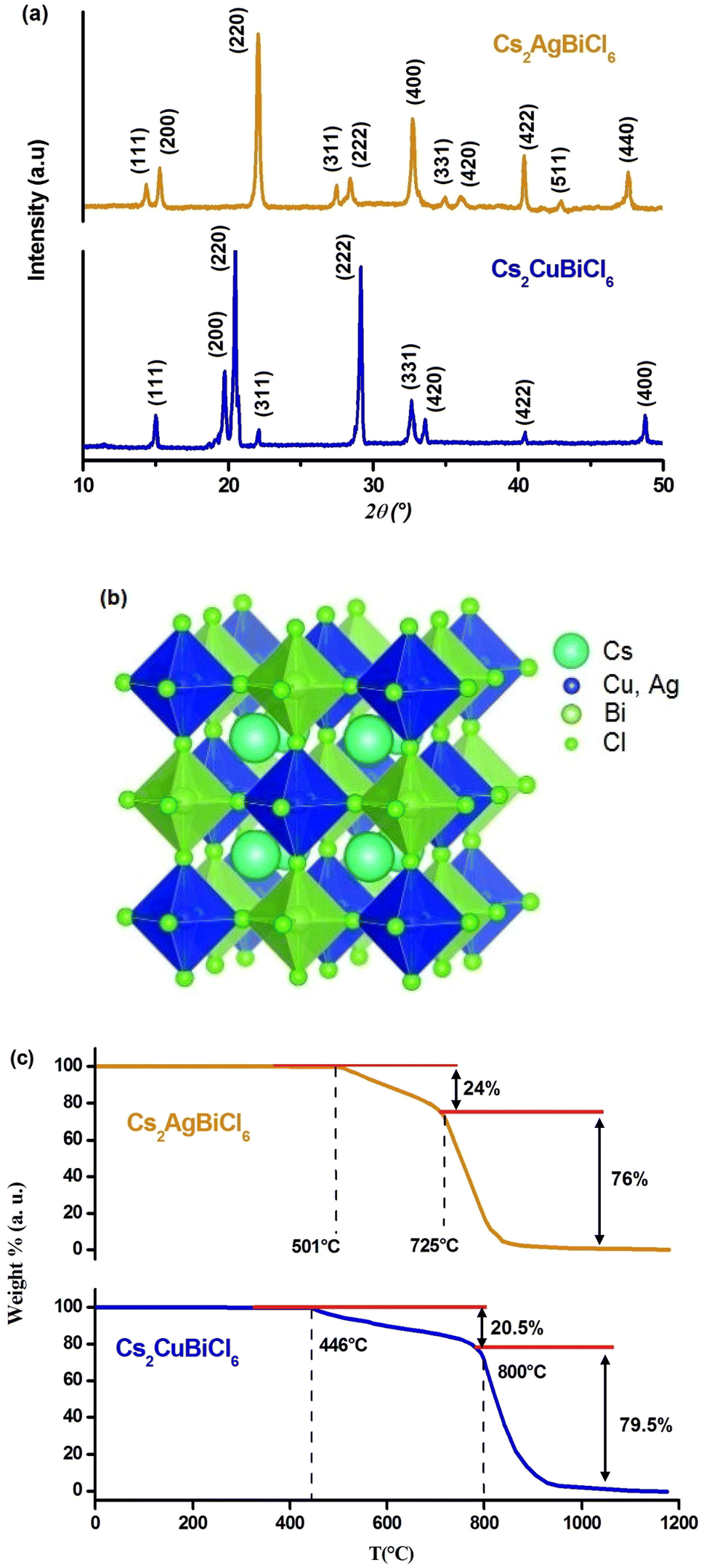 | ||
| Fig. 1 (a) Powder X-ray diffractogram of Cs2MBiCl6 (M = Cu, Ag) at room temperature in the 2θ range 10–50°. (b) Constructed cubic crystal structure of Cs2MBiCl6 (M = Cu, Ag). (c) TG data of Cs2MBiCl6 (M = Cu, Ag) in the temperature range of 100–1190 K. | ||
The perovskites under consideration have been characterized with an electronic dimensionality of 0D due to the spatial separation observed between the [MCl6]5− and [BiCl6]3− octahedra. This 0D electronic dimensionality leads to the confinement of photoexcited charge carriers, resulting in high effective masses of charge carriers.23
In light of the significance of thermal stability as a crucial property for future applications of halide perovskites, we conducted thermogravimetric analysis on Cs2MBiCl6 (M = Cu, Ag) powder samples prepared for this study (Fig. 1(c)). Our analysis revealed a noticeable weight loss occurring in two distinct stages.
The initial stage weight loss was observed in the temperature range of 446/501 to 800/725 °C and can be attributed to the evaporation of CsMCl2 (M = Cu, Ag).24 Hence, the decomposition process can be described as follows: Cs2MBiCl6 (M = Cu, Ag) CsMCl2 + CsBiCl4. The subsequent weight loss of 76/79.5 wt% at 800/725 °C is associated with the evaporation of CsCl and MCl (M = Cu, Ag).24 The decomposition reaction can be represented by the following scheme: CsBiCl4 CsCl + BiCl3.
The findings presented above suggest that Cs2MBiCl6 (M = Cu, Ag) exhibits a notable level of stability up to approximately 446/501 °C, which holds significant implications for its extensive applications in optoelectronic and photochemical fields.25 However, beyond this temperature, noticeable decomposition reactions take place, leading to the complete loss of material functionality.
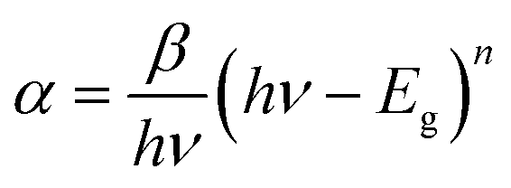
The optical absorption of Cs2MBiCl6 compounds (where M = Ag, Cu) was estimated within a wavelength range of 300–800 nm using a UV-Vis spectrophotometer (Fig. 2(a) and (b)). We have determined an indirect bandgap (Eg) of 1.31 eV and 2.91 eV for Cs2CuBiCl6 and Cs2AgBiCl6 (inset in Fig. 2(a) and (b)) by Tauc relation, which is expressed as:26–30
 | (1) |
 | ||
| Fig. 2 Absorption spectra of (a) Cs2CuBiCl6 and (b) Cs2AgBiCl6. The inset shows the Tauc plot. | ||
The significant absorption observed in the visible region indicates that Cs2MBiCl6 (where M = Ag, Cu) materials have the ability to effectively harness solar energy, enabling the generation of an ample number of photoinduced electron–hole pairs.25 This characteristic promotes photoactivity by facilitating the desired reactions.25
Based on the Tauc formula presented below, it is possible to estimate the optical bandgap Eg:
| (αhν)1/n = β(hν − Eg) | (2) |
When n = 2, the best plots are obtained by plotting (αhν)2 and (αhν)1/2 against photon energy (hν), leading to the most satisfactory results. In accordance with the Tauc equation, the indirect transition was then chosen:
| (αhν)2 = β(hν − Eg) | (3) |
The bandgap Eg value can be determined by extrapolating the linear portion to α = 0,31 as demonstrated in the inset of Fig. 2(a) and (b) with Eg values of 1.31 eV and 2.91 eV for Cs2CuBiCl6 and Cs2AgBiCl6, respectively, these materials are promising candidates for optoelectronics.
The following equation can be used to determine the optical bandgap transition mode of our compound:32
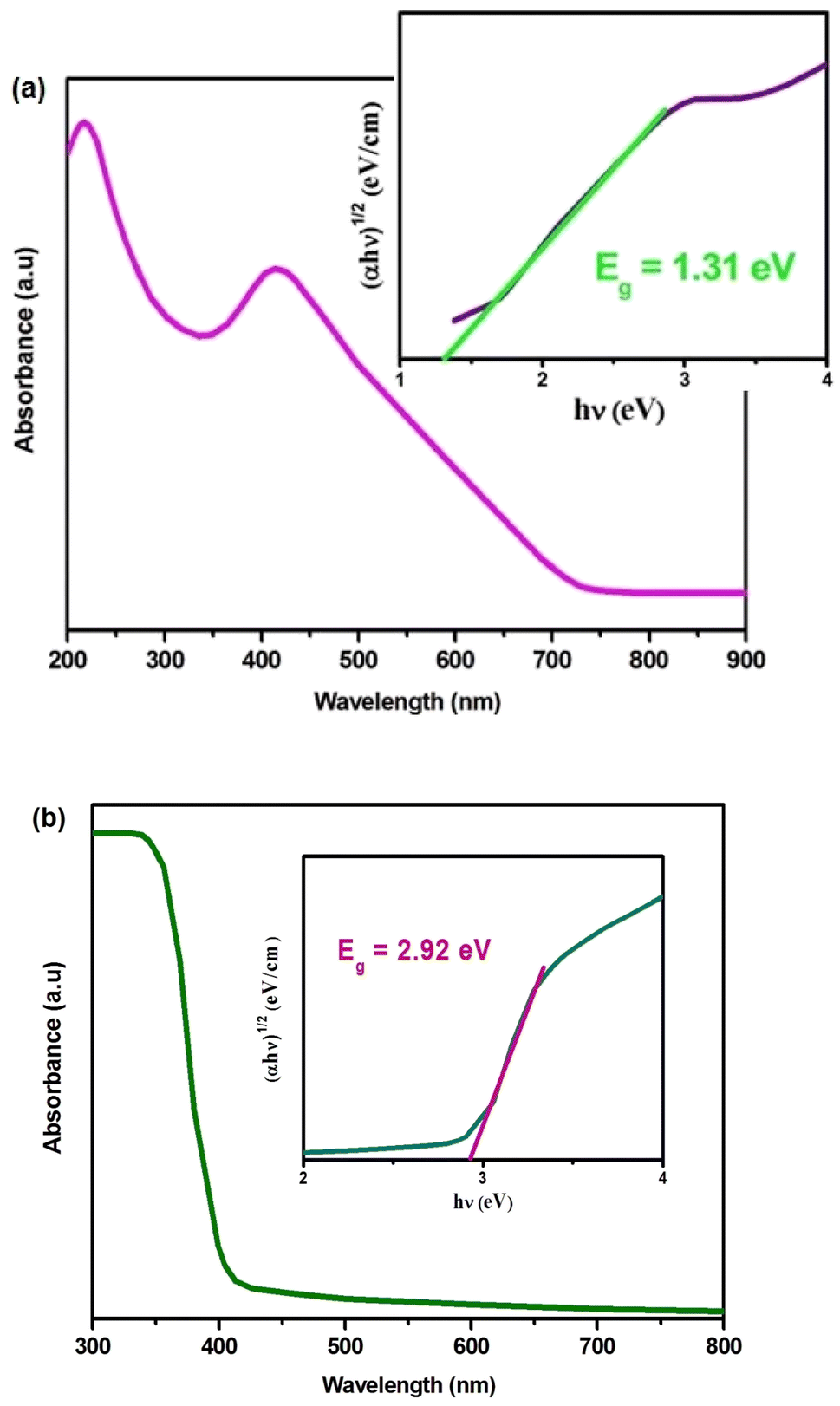
ln(αhν) = ln(β) + n![[thin space (1/6-em)]](https://www.rsc.org/images/entities/char_2009.gif) ln(hν − Eg) ln(hν − Eg)
| (4) |
The plots of ln(αhν) vs. ln(hν − Eg) are shown in Fig. 3(a) and (b). The slope of the resulting straight line indicates the power factor (n), which identifies the type of optical transition mode.32 Using eqn (5) and the data from Fig. 3(a) and (b), we obtained the following linear relationships:
|
ln(αhν) = 16.69 + 1.98ln(hν − 1.31); (n ≈ 2) (Cs2CuBiCl6)
| (5) |
|
ln(αhν) = 14.07 + 1.92ln(hν − 2.92); (n ≈ 2) (Cs2AgBiCl6)
| (6) |
 | ||
| Fig. 3 Curves of ln(αhν) vs. ln(hν − Eg) for (a) Cs2CuBiCl6 and (b) Cs2AgBiCl6. | ||
Thus, the indirect transition modes of the optical band of Cs2CuBiCl6 and Cs2AgBiCl6 were confirmed, as shown by the calculated transition power factor (n) values, which were found to be close to 2, in agreement with the expected modes.
The temperature-dependent behavior of the real part (Z′) of the complex impedance with varying frequencies is depicted in Fig. 4(a) and (b) for different temperatures. As temperature and frequency increase, Z′ decreases, indicating the negative temperature coefficient of resistance (NTCR) behavior in both Cs2MbiCl6 (M = Ag, Cu) materials.33,34 This behavior suggests that the AC conductivity may increase due to a decrease in the trapped charge density and an increase in the mobility of charge carriers within the material. At high frequencies, the temperature-independent behavior of Z′ indicates the presence of space charge in both materials. The reduction in the relaxation time of the space charge at higher frequencies results in the merging of curves due to the collapse of space charge polarization.35 The graphs in Fig. 5(a) and (b) illustrate the variation of the loss factor (Z′′) in both double perovskite materials across the frequency range and various temperatures. These variations provide insight into the relaxation process and the fundamental charge transport mechanism of the materials. At high temperatures, the relaxation process is caused by defects or vacancies, while at low temperatures, it is due to immobile species or electrons. Each spectrum shows a distinct characteristic peak known as the “relaxation frequency.” The broadness of the peak suggests a deviation from the ideal Debye nature. The charge carrier motion over a long range is the main cause of transportation below the loss peak frequency, while above the relaxation frequency, the movement of the localized carriers is promoted. The relaxation peak shifts towards the high-frequency range with an increase in temperature, indicating a thermally dependent relaxation mechanism. The peak height decreases with temperature, suggesting a decline in grain and grain boundary resistance with temperature.36
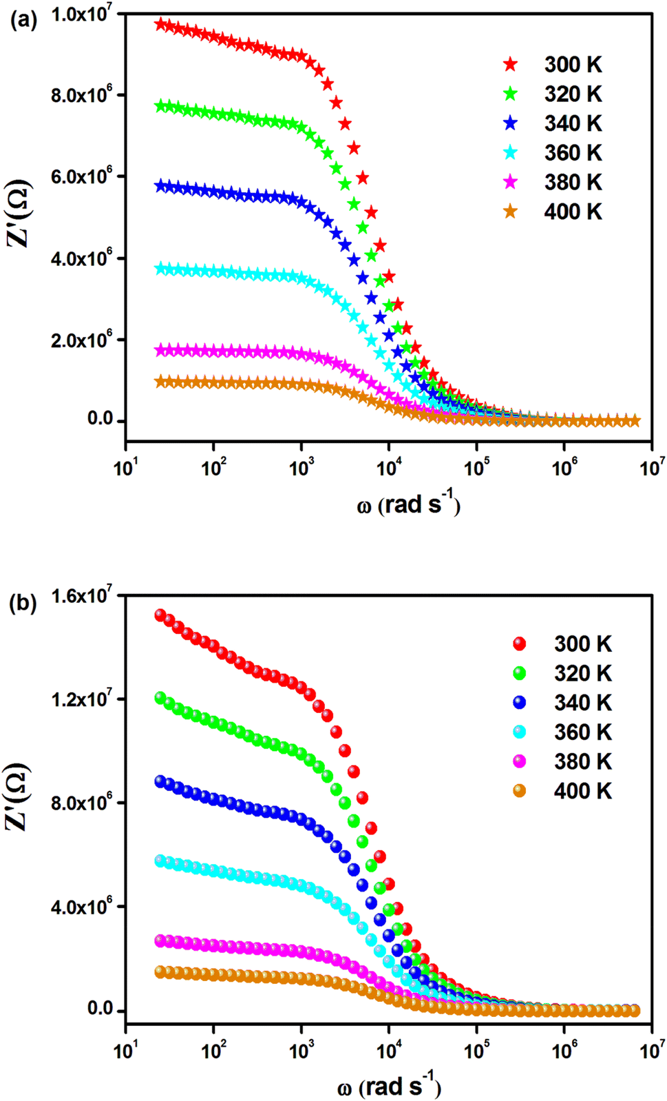 | ||
| Fig. 4 Frequency dependence of Z′(ω) for (a) Cs2CuBiCl6 and (b) Cs2AgBiCl6 at various temperatures. | ||
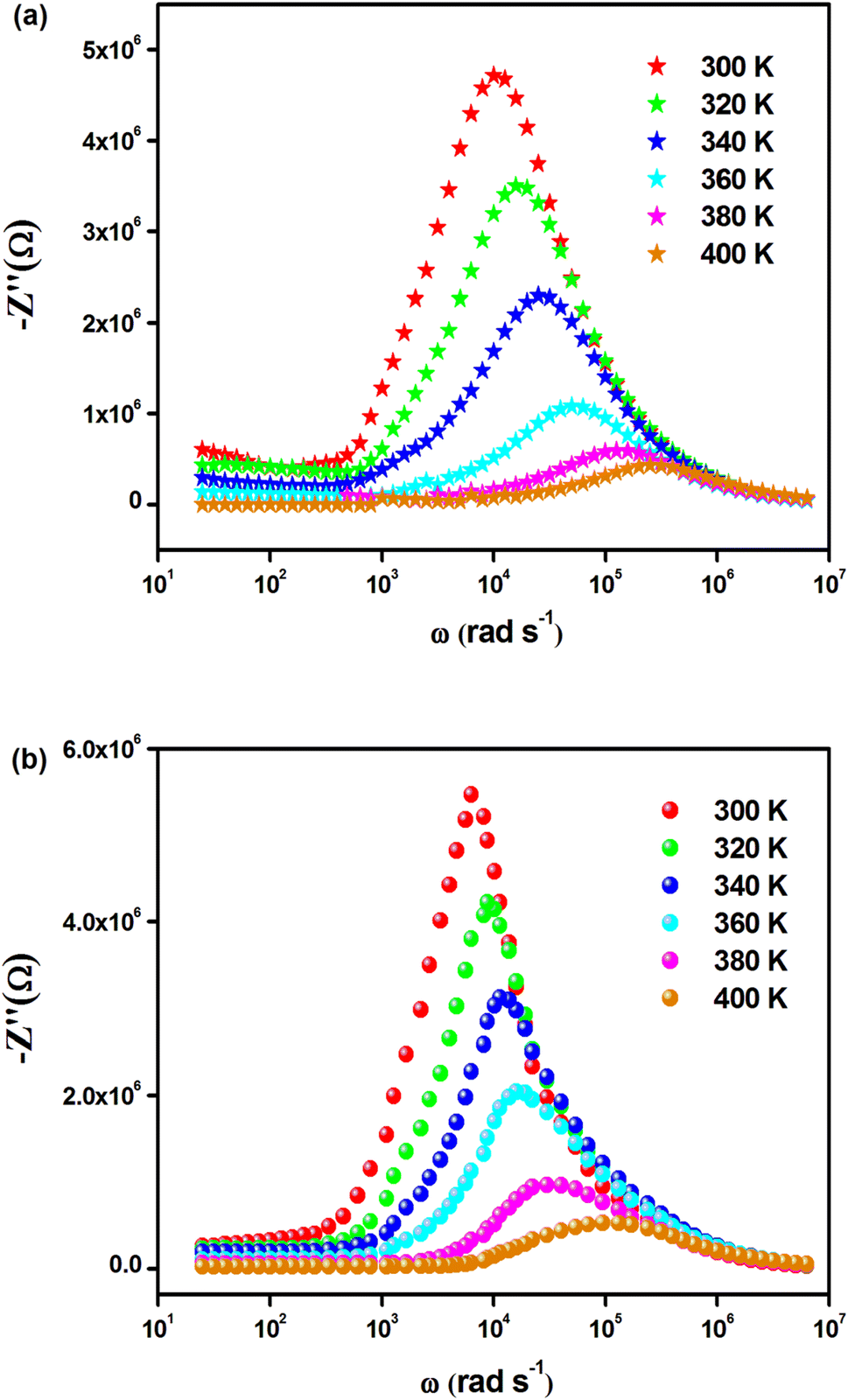 | ||
| Fig. 5 Frequency dependence of Z′′(ω) for (a) Cs2CuBiCl6 and (b) Cs2AgBiCl6 at various temperatures. | ||
Fig. 6(a) and (b) depict the Cole–Cole plot between 300 and 400 K. It is worth noting that the centers of the depressed semicircles lie below the real axis, indicating that both materials exhibit non-Debye behavior. Additionally, as the temperature increases in the Cole–Cole plot, the radii of the semicircles decrease, providing further evidence of the NTCR behavior of Cs2MBiCl6 (M = Ag, Cu).36,37 This suggests that these compounds exhibit properties of semiconductors and that the conduction mechanism is thermally activated. The Nyquist plot ideally displays three separate semicircles that represent the contribution of the grains, grain boundaries, and electrode-material interface. The semicircle observed in the high-frequency region corresponds to the contribution of the grains, while the semicircle in the low-frequency region corresponds to the contribution of the grain boundaries. Additionally, the semicircle in the ultra-low-frequency region confirms the contribution of the electrode-material interface. Distinguishing the contribution of grains and grain boundaries from a single depressed semicircle is difficult. To solve this problem, researchers have used the Maxwell–Wagner equivalent circuit model, which is made up of a parallel combination of resistors (R) and capacitors (C). To obtain the desired circuit model for Cs2MBiCl6 (M = Ag, Cu), two parallel RC elements are connected in series. The ZView software is used to fit the impedance spectra of all temperatures. In addition, a constant phase element (CPE) is used to interpret the straight line that follows the semicircle, which depends on the double layer capacity of an inhomogeneous electrode surface (see the insets in Fig. 6(a) and (b)). Fig. 6(a) and (b) depict a significant decrease in the diameter of the semicircle and its intersection point on the real axis with an increase in temperature, indicating an enhancement in DC conductivity of Cs2MBiCl6 (M = Ag, Cu).38 A schematic representation of the grains and grain boundaries is depicted in Fig. 6(c). To evaluate these parameters, the experimental data were fitted using the ZView software. Table 1 shows that Rgb values are higher than Rg values at all temperatures, implying that grain boundaries have a greater contribution to the total resistance. This difference between the resistive values causes an increase in the number of space charges at the grain boundaries due to polarization, leading to the Maxwell–Wagner effect.39 It is well known that grain boundaries are more resistive than grains in perovskite materials.17
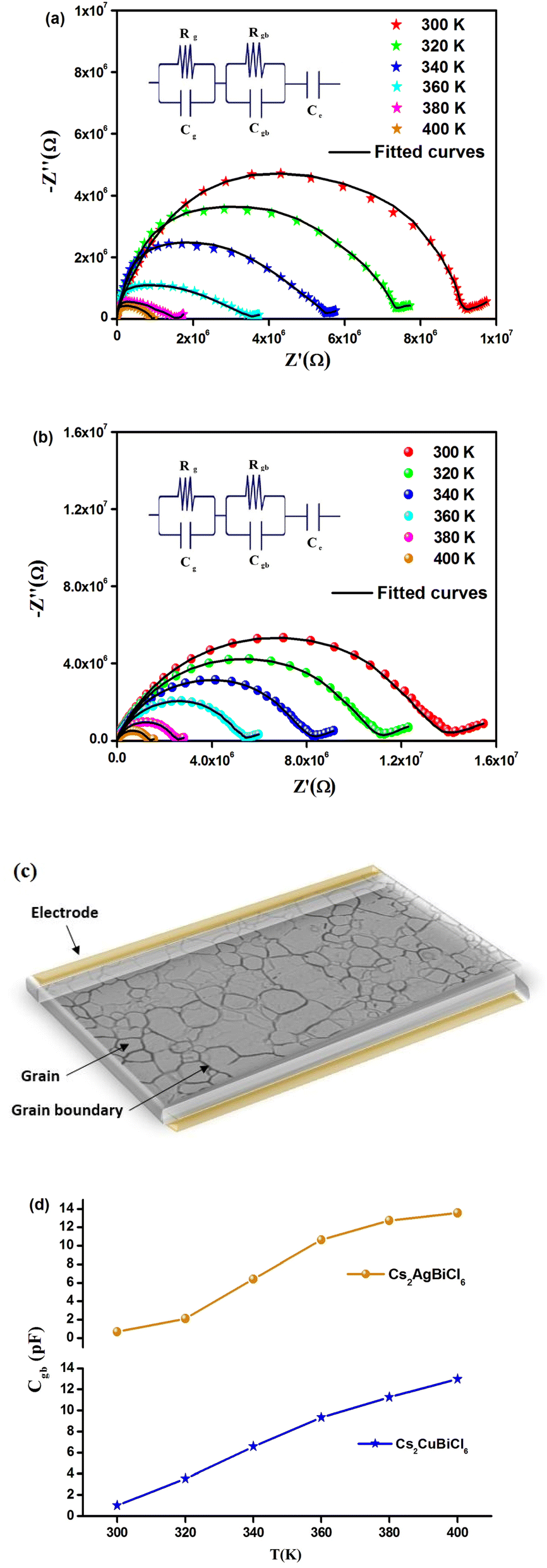 | ||
| Fig. 6 Fitted Cole–Cole plots of (a) Cs2CuBiCl6 and (b) Cs2AgBiCl6 at different temperature, (the equivalent circuits have shown in inset). (c) Representation of grain and grain boundary within material. (d) The variation of Cgb of Cs2MBiCl6 (M = Cu, Ag) at different temperatures. | ||
| Temperature (K) | Rg (kΩ) | Cg (nF) | Rgb (kΩ) | Cgb (pF) | CPEe (μF) | αe |
|---|---|---|---|---|---|---|
| Cs2CuBiCl6 | ||||||
| 300 | 402 | 1.32 | 8904 | 1.00 | 0.98 | 0.575 |
| 320 | 302 | 1.45 | 7012 | 3.54 | 1.12 | 0.478 |
| 340 | 198 | 1.94 | 5786 | 6.57 | 1.47 | 0.486 |
| 360 | 87 | 2.12 | 4258 | 9.33 | 1.70 | 0.502 |
| 380 | 12 | 2.64 | 3112 | 11.25 | 1.96 | 0.511 |
| 400 | 0.77 | 2.80 | 1254 | 12.99 | 2.08 | 0.562 |
|
||||||
| Cs2AgBiCl6 | ||||||
| 300 | 756 | 1.05 | 11355 |
0.68 | 0.47 | 0.685 |
| 320 | 541 | 1.65 | 9012 | 2.11 | 0.82 | 0.625 |
| 340 | 356 | 2.05 | 7452 | 6.39 | 1.05 | 0.574 |
| 360 | 105 | 2.97 | 5214 | 10.62 | 1.18 | 0.623 |
| 380 | 74 | 3.44 | 3879 | 12.73 | 1.25 | 0.542 |
| 400 | 3.56 | 4.61 | 2652 | 13.54 | 1.31 | 0.598 |
The trends in grain boundary capacitance (Cgb) with temperature are shown in Fig. 6(d) for both materials. The expression for Cgb is given by Cgb = (εgbA)/d, where εgb represents the intrinsic dielectric constant at the grain boundary, A is the area of the grain boundary, and d is the barrier-layer width. The barrier-layer width is proportional to the ratio of the trapped charge carriers to free carrier density.17 As temperature increases, trapped charge carriers decrease, resulting in a smaller barrier-layer width. Consequently, the grain boundary capacitance increases with temperature due to this behavior.
The investigation of the dielectric constants within the temperature range of 300 to 400 K and as a function of frequency is demonstrated in Fig. 7(a)–(d). It is shown that the dielectric constant in the low-frequency region is significant at a specific temperature and declines gradually with an increase in frequency for both materials. The ionic conduction process is influenced by both ε′(ω) and ε′′(ω) and is driven by four types of polarization; namely, interfacial, orientational, electronic, and ionic polarization. Interfacial and orientational polarizations refer to the relaxation component of polarizability, whereas electronic and ionic polarizations represent the deformational component of polarizability.40 The changes in the real part of permittivity with frequency are influenced by Maxwell–Wagner interfacial polarization, which is consistent with Koop's phenomenological theory.41 This theory suggests that the material contains conducting grains separated by poorly conducting grain boundaries, resulting in trapped charge carriers at the interfaces of grain boundaries and hindering their flow.41,42 The interfacial polarization process involves the exchange of electrons between the ions of the same molecules. Imperfections and deformities within the material result in changes in the position and distribution of positive and negative space charges. Under the influence of the applied electric field, positive charges move towards the negative poles, while negative charges move towards the positive poles.43 It is observed that in the low-frequency range, these materials permit electrons to reach the grain boundary regime via hopping (Fig. 7(a) and (b)). However, due to the high resistance at the grain boundary, the electrons are accumulated at the grain boundary and induce polarization. On the other hand, at high frequencies, the electrons are unable to follow the changes in the applied field and as a result, they cannot accumulate further, even though they move in the opposite direction. Therefore, with decreasing polarization thickness, there is a reduction in the likelihood of electrons reaching the grain boundary as the frequency increases.18 In the mid-frequency region, the variation in ε′(ω) may exhibit a hump due to the relaxation process. A temperature-dependent dielectric response is brought about by the shift of the hump position to the low-frequency region as the temperature increases. However, the value of ε′(ω) at high frequency remains relatively unchanged. The “unrelaxed” value of permittivity indicates the contribution of atomic and electronic polarization. In the double perovskite material Cs2MBiCl6, polarization is primarily determined by the presence of Cs+, [MCl6]5−, and [BiCl6]3− ions. As the temperature decreased, the real part of the dielectric constant ε′(ω) also decreased. This could be attributed to the reduced mobility of conducting electrons and participating ions at lower temperatures.
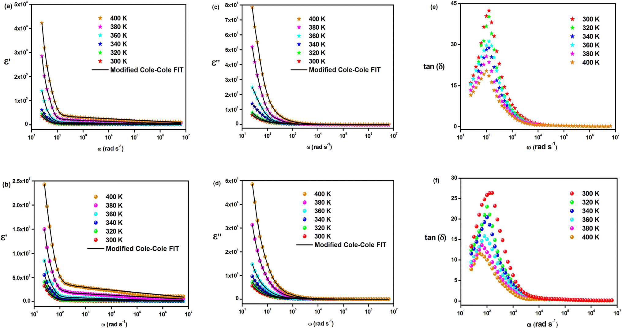 | ||
| Fig. 7 Variation of ε′(ω) of (a) Cs2CuBiCl6 and (b) Cs2AgBiCl6 at different temperatures. Variation of ε′′(ω) of (c) Cs2CuBiCl6 and (d) Cs2AgBiCl6 at various temperatures. Frequency-dependent dielectric loss (tanδ) of (e) Cs2CuBiCl6 and (f) Cs2AgBiCl6. | ||
One of the popular theoretical models, the modified Cole–Cole model, has been utilized along with DC conductivity to study the change in dielectric constant and dielectric loss with frequency for different temperatures. The complex permittivity can be expressed using the modified Cole–Cole model, as shown below:17
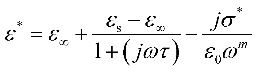 | (7) |
 | (8) |
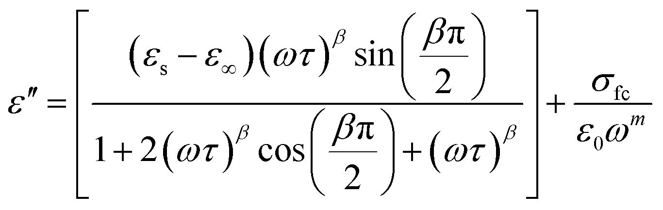
The symbol σ* denotes the combination of the conductivities of free charge carriers (σfc) and space charge carriers (σsp). The limit of permittivity at high frequency is represented by ε∞, while εs refers to the limit of permittivity at low frequency. The relaxation time is indicated by τ, and the frequency exponent is denoted by m. The modified Cole–Cole parameter, β, ranges from 0 to 1. Eqn (9) and (10) demonstrate the real (ε′) and imaginary (ε′′) components of the dielectric constant.44,45
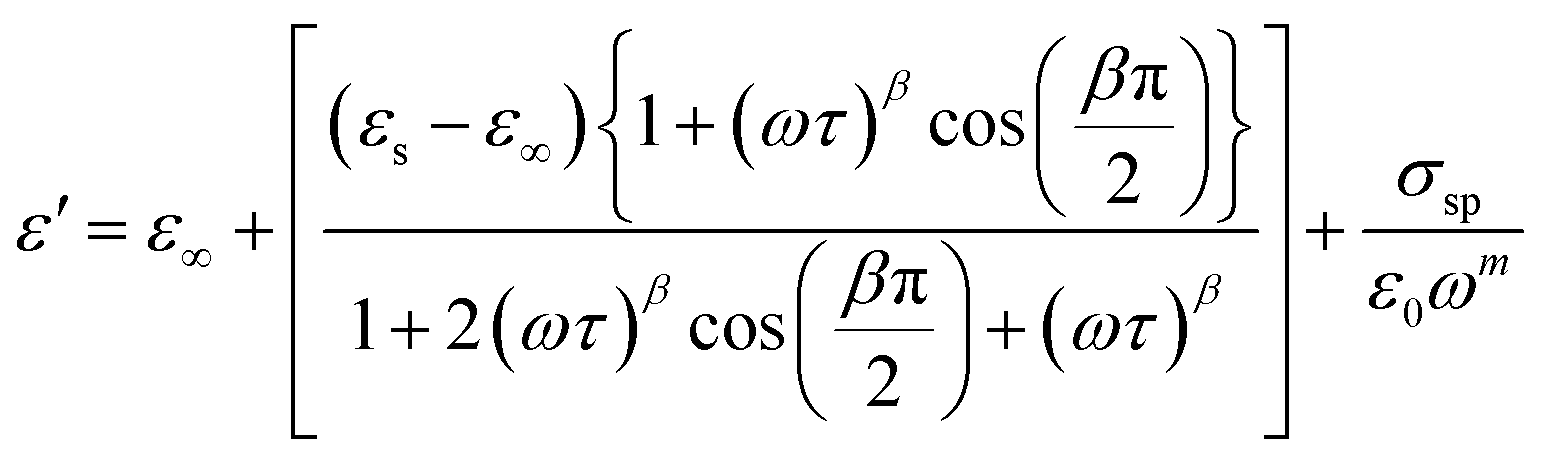 | (9) |
 | (10) |
The modified Cole–Cole equation was used to fit the experimental data of ε′ and ε′′. The obtained values for various parameters such as β, m, σsp, σfc, and τ are presented in Table 2. It is evident from the table that the values of free charge conductivity (σfc) and space charge conductivity (σsp) for Cs2MBiCl6 (M = Ag, Cu) increase as the temperature rises. The value of β, which ranges between 0 and 1, indicates the non-Debye nature. As the temperature increases, the relaxation time decreases.
| Parameter | Temperature | |||||
|---|---|---|---|---|---|---|
| 300 K | 320 K | 340 K | 360 K | 380 K | 400 K | |
| Cs2CuBiCl6 | ||||||
| τ | 9.65 × 10⁻³ | 5.32 × 10⁻³ | 2.17 × 10⁻³ | 7.91 × 10⁻⁴ | 3.46 × 10⁻⁴ | 8.87 × 10⁻⁵ |
| β | 0.786 | 0.684 | 0.725 | 0.805 | 0.632 | 0.854 |
| m | 0.785 | 0.799 | 0.805 | 0.823 | 0.841 | 0.878 |
| σsp | 1.58 × 10⁻⁵ | 4.74 × 10⁻⁵ | 7.99 × 10⁻⁵ | 2.66 × 10⁻⁴ | 6.79 × 10⁻⁴ | 1.41 × 10⁻³ |
| σfc | 7.56 × 10⁻³ | 5.69 × 10⁻³ | 1.90 × 10⁻³ | 8.57 × 10⁻² | 3.38 × 10⁻² | 9.85 × 10⁻¹ |
|
||||||
| Cs2AgBiCl6 | ||||||
| τ | 1.15 × 10⁻² | 6.08 × 10⁻³ | 2.79 × 10⁻³ | 9.53 × 10⁻⁴ | 7.25 × 10⁻⁴ | 4.67 × 10⁻⁴ |
| β | 0.966 | 0.644 | 0.715 | 0.734 | 0.879 | 0.654 |
| m | 0.844 | 0.859 | 0.870 | 0.896 | 0.903 | 0.911 |
| σsp | 9.87 × 10⁻⁵ | 3.54 × 10⁻⁴ | 8.81 × 10⁻⁴ | 2.07 × 10⁻³ | 9.44 × 10⁻³ | 2.79 × 10⁻² |
| σfc | 6.69 × 10⁻³ | 1.73 × 10⁻³ | 4.87 × 10⁻² | 8.45 × 10⁻¹ | 5.55 × 10⁻¹ | 2.13 × 10⁻¹ |
The loss tangent refers to the ratio of the dielectric loss to the real part of the dielectric constant. Fig. 7(e) and (f) show the variation in the loss tangent with frequency for a specific temperature range (tan(δ) = ε′(ω)/ε′′(ω)). Cs2MBiCl6 (M = Ag, Cu) exhibits a decrease in the loss tangent with increasing frequency, which ultimately becomes constant at a certain temperature in the high-frequency region. At low frequencies, the observed peaks are likely a result of dominant dipolar polarization. As the loss tangent values increase, the peaks shift with increasing temperature, providing evidence that dipolar polarization is influenced by temperature. The loss peak eventually appears when the hopping frequency corresponds to the frequency of an applied external AC field. Additionally, the hopping mechanism implies that as the temperature increases, the electrical conductivity also increases, leading to the activation of charge carriers through thermal means.
Fig. 8(a) and (b) demonstrate the frequency dependence of the real part of the electric modulus spectra for different temperatures. As shown in these figures, M′ is nearly zero at low frequencies for all temperatures. This behavior can be attributed to the long-range mobility of charge carriers in the conduction mechanism and the neglect of electrode polarization. In addition, the sigmoidal nature of M′ is evident. The peak of M′ shows a slight shift towards higher frequencies as the temperature increases in the high-frequency region.
 | ||
Fig. 8 Variation of M′(ω) of (a) Cs2CuBiCl6 and (b) Cs2AgBiCl6 at different temperatures. Variation of M′′(ω) of (c) Cs2CuBiCl6 and (d) Cs2AgBiCl6 at various temperatures. (e) Arrhenius plots of Cs2MBiCl6 (M = Cu, Ag). Normalized imaginary modulus  vs. f/fmax of (f) Cs2CuBiCl6 and (g) Cs2AgBiCl6 at various temperatures. vs. f/fmax of (f) Cs2CuBiCl6 and (g) Cs2AgBiCl6 at various temperatures. | ||
The variation in the imaginary part of the electric modulus spectra (M*) with frequency at different temperatures is depicted in Fig. 8(c) and (d). A peak occurs in M* at a frequency that corresponds to the relaxation frequency, and at a certain temperature, M* reaches its maximum value. There is no peak in the low-frequency region, while there is a significant peak in the high-frequency region. The charge carriers show successful hopping from one site to another, which enables them to move over a long distance in the low-frequency region. At high frequencies, the mobility of charge carriers is limited as they are confined within their potential well, causing them to move in a controlled manner. Hence, the appearance of peaks in the complex modulus spectra indicates the transition from long-range to short-range mobility of charge carriers. The shift of the peaks in the imaginary part of the electric modulus to higher frequencies with increasing temperature indicates the hopping mechanism. The non-Debye response of the sample is demonstrated by the asymmetric nature of the peaks in M′′. The asymmetric nature of the peaks is explained using the KWW equation, as shown in eqn (11):44,45
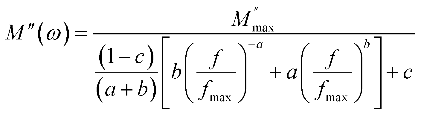 | (11) |
The frequency at which M′′ reaches its maximum value is denoted as fmax, while the maximum value of M′′ is represented by 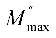 . The two distinct parameters that shape the low-frequency and high-frequency sides are a and b, respectively. Additionally, c denotes the smoothing parameter. If a = b = 1 and c = 0, eqn (11) reduces to eqn (12), which corresponds to the ideal Debye behavior and displays the symmetrical nature of M′′ spectra with respect to frequency. Fig. 8(c) and (d) demonstrate that the modified KWW function fits well, as indicated by the solid line. Table 3 provides the respective parameter values. The data show that, as the temperature rises, both a and b values increase, indicating that M′′(ω) approaches an ideal Debye-type response at higher temperatures.
 | (12) |
| Temperature (K) | a | b |
|---|---|---|
| Cs2CuBiCl6 | ||
| 300 | 0.478 | 0.347 |
| 320 | 0.529 | 0.388 |
| 340 | 0.593 | 0.437 |
| 360 | 0.614 | 0.530 |
| 380 | 0.687 | 0.627 |
| 400 | 0.770 | 0.701 |
|
||
| Cs2AgBiCl6 | ||
| 300 | 0.547 | 0.572 |
| 320 | 0.653 | 0.602 |
| 340 | 0.741 | 0.640 |
| 360 | 0.798 | 0.681 |
| 380 | 0.802 | 0.704 |
| 400 | 0.825 | 0.712 |
Eqn (13) is utilized to determine the relaxation time (τ).
 | (13) |
The Arrhenius formula below is employed to calculate the average activation energies of the charge carriers:
 | (14) |
The activation energies of the charge carriers in Cs2AgBiCl6 and Cs2CuBiCl6 were determined using the Arrhenius equation (eqn (14)) and the ln(τ) vs. 1000/T curves are shown in Fig. 8(e). The calculated activation energies were 0.222 eV and 0.338 eV, respectively. This suggests that the conduction mechanism in both materials is attributable to the thermally-stimulated charge carriers.46
Fig. 8(f) and (g) depict the changes in the normalized imaginary part of the electric modulus and the normalized frequency of the samples at different temperatures. The peak positions in the normalized spectrum indicate a shift from long-range to short-range mobility of the charge carriers, as well as the hopping method of charge carriers, which was previously described in detail in the case of M′′ spectra.47 The peak coincidences at all temperatures suggest that the dynamic processes occurring in Cs2MBiCl6 (M = Ag, Cu) are independent of temperature.
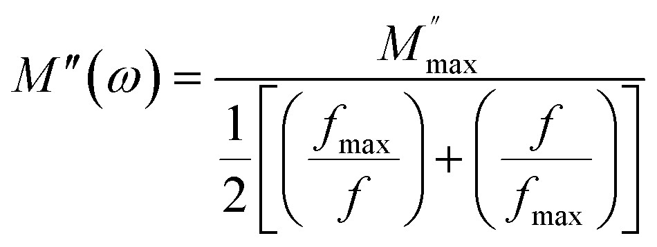
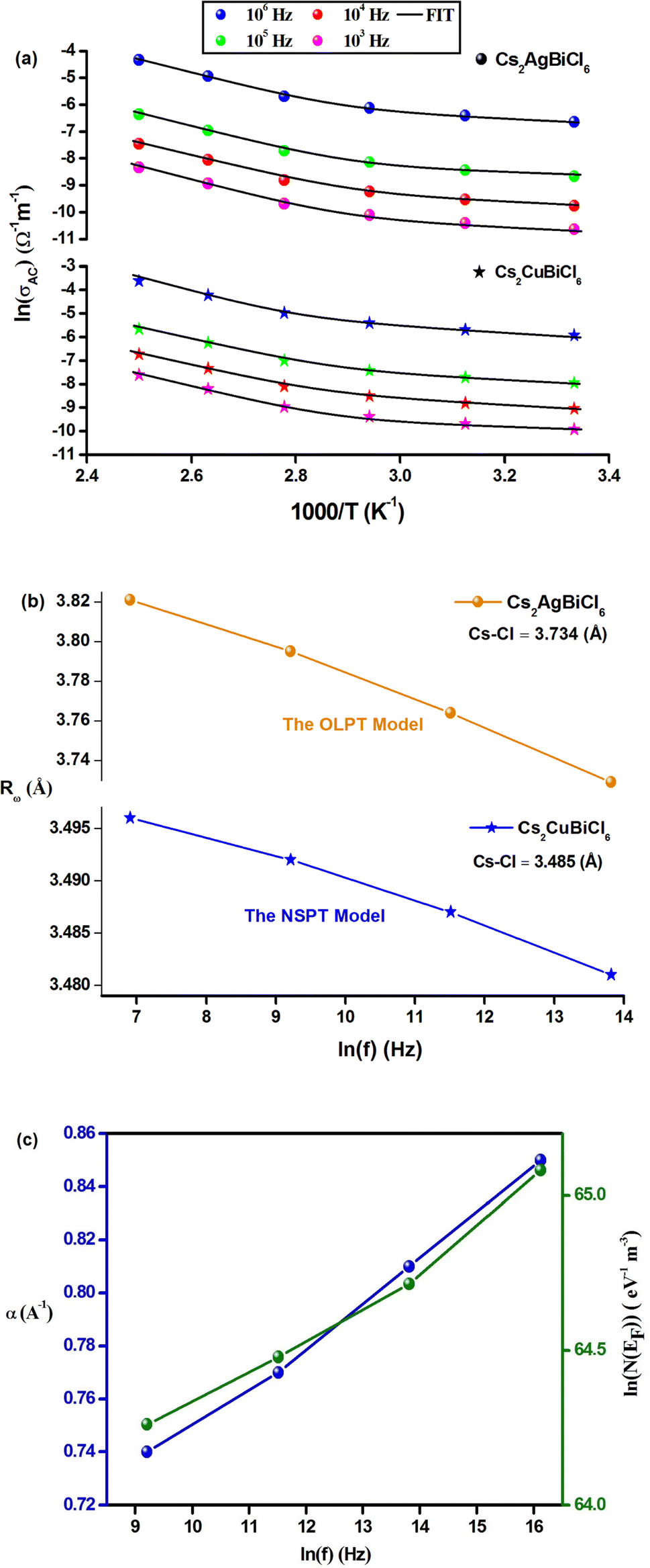
Fig. 9(a) and (b) demonstrate the temperature-dependent changes in AC conductivity versus frequency. The AC electrical conductivity is estimated using the following formula: σac = ωε′ε0tanδ, where ε0 represents the permittivity of free space. AC conductivity contributes to the overall conductivity in the high-frequency range, while DC conductivity accounts for the calculated conductivity in the low-frequency range. The curves appear to flatten in this range due to the temperature-dependent and frequency-independent DC conductivity. However, the electrical conductivity curves increase significantly and exhibit significant frequency dispersion with increasing frequency, owing to the contribution of AC conductivity. The frequency at which the conductivity transition occurs in this type of behavior is referred to as “frequency hopping” (ωP). As the temperature increases, ωP shifts to the high-frequency range. Funke's jump relaxation model (JRM) can explain the observed frequency-dependent AC conductivity and frequency-independent DC conductivity.48 According to JRM, at low frequencies, ions can hop to adjacent sites, resulting in long-range translational motion that contributes to DC conductivity, which is sustained over a long period. However, in the high-frequency range, hopping can result in either successful or unsuccessful outcomes.
 | ||
| Fig. 9 The variation of σac with frequency at different temperatures for (a) Cs2CuBiCl6 and (b) Cs2AgBiCl6. (c) Arrhenius plots of dc conductivity for Cs2MBiCl6 (M = Cu, Ag). (d) Temperature dependence of s and 1 − s for Cs2MBiCl6 (M = Cu, Ag). | ||
In unsuccessful hopping, the hopping ion can move back and forth before returning to its initial position, whereas in successful hopping, the excited hopping ion jumps to a new site and remains stationary, causing the surrounding ions to relax. At high frequencies, the proportion of unsuccessful to successful hopping increases, resulting in dispersive conductivity. The measured electrical conductivity is attributed to Jonscher's power law and the universal dielectric response (UDR) model developed by Jonscher:49
| σAC(ω) = σDC + σ0fs | (15) |
The total conductivity comprises DC and AC contributions denoted by σDC and σAC, respectively, while σ0 is a constant and the frequency exponent is represented by the parameters. The parameter “s” reflects the extent to which charge carriers interact with the lattice of Cs2MBiCl6 (M = Ag, Cu) and falls within the range of 0 to 1.
The experimental data of the σAC(ω) variation (Fig. 9(a) and (b)) were fitted using the UDR approach to determine the σDC values at all temperatures for both materials. Based on Fig. 9(c) (ln(σDC) vs. 1000/T), the average activation energies of Cs2MBiCl6 (M = Ag, Cu) can be calculated using the following Arrhenius equation:
 | (16) |
The activation energy values for Cs2AgBiCl6 and Cs2CuBiCl6 are 0.236 eV and 0.359 eV, respectively. It should be noted that these values are similar to those obtained from the modulus analysis.
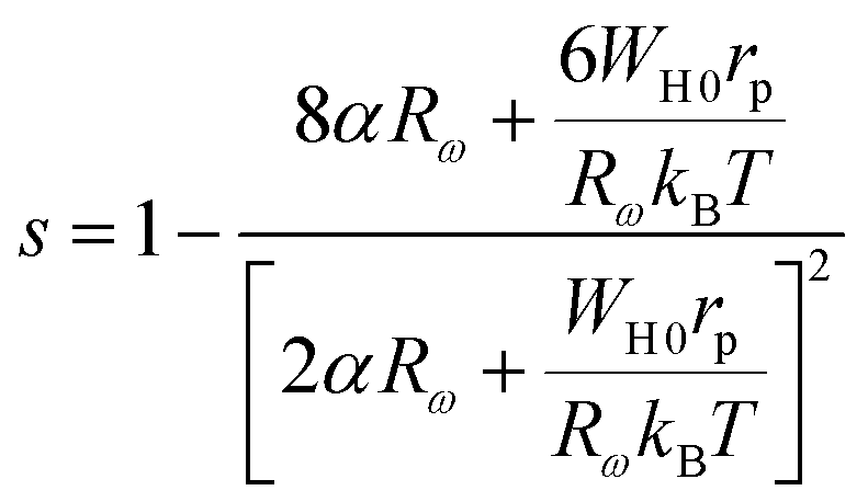
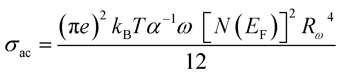
A proposed pattern for understanding the charge transfer mechanism in Cs2MBiCl6 (M = Ag, Cu) can be developed by considering various theoretical approaches related to the evolution of s(T). In the literature, several models have been suggested based on different methods, such as quantum mechanical tunneling, typical barrier hopping, or a combination of the two, which are consistent with the data. Furthermore, it is hypothesized that there are different types of carriers, such as electrons (or polarons) or atoms. Various theoretical approaches are proposed based on quantum mechanical tunneling, typical barrier hopping, or a combination of the two, which include overlapping large polaron tunneling (OLPT), non-overlapping small-polaron tunneling (NSPT), correlated barrier hopping (CBH), and quantum mechanical tunneling (QMT).50–53 Fig. 9(d) displays the temperature-dependent variation of the exponent ‘s’ for Cs2MBiCl6 (M = Ag, Cu) double perovskite materials:
• For Cs2AgBiCl6, as the parameter ‘s’ decreases with increasing temperature to a minimum value and then slightly increases, it suggests that the OLPT approach is suitable.
• For Cs2CuBiCl6, since the parameter ‘s’ increases with temperature, the NSPT approach is deemed appropriate.
When a localized charge approaches the material, polarons are formed and they move to the nearest adjacent positions. Once a polaron reaches a new configuration, it can remain stable in that position after a successful hop, or it can shift back to its original position after an unsuccessful hop. The non-dispersive behavior of AC conductivity in the low-frequency region is due to successful polaron hopping. However, at higher frequencies, an increasing number of hops become unsuccessful, leading to dispersive (AC) conductivity. It is suggested that in many perovskite compounds, the formation of a polaron occurs via lattice deformation,27 which is not accounted for in electron tunneling models. Creating polarons can cause a significant distortion in the local lattice, due to the high degree of charge transport at a site. This distortion can be so significant that it prevents the overlapping of polaron clouds. At higher temperatures, the (AC) conductivity is attributed to confined polarons at structural defects or carrier tunneling.18
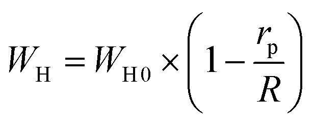
The OLPT approach interprets the (AC) conductivity as the process of polaron tunneling, which occurs when the polaron distortion clouds overlap. In the case of large polarons, the interatomic spacing is smaller than the spatial extent of the polaron. In some instances, the long-range Coulomb interaction results in the overlap of the potential wells at nearby sites, reducing the polaron hopping energy. As a result, the loss is affected by the frequency, and the activation energy associated with the motion of charge carriers between different sites decreases, as shown in eqn (17):50
 | (17) |
The energy required for polaron hopping is denoted by WH, while rp indicates the radius of the large polaron. It should be noted that WH represents the polaron hopping energy.
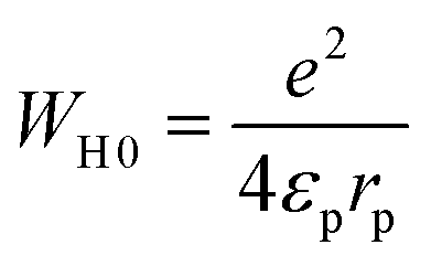
Eqn (18) demonstrates the expression for the energy WH0:51
 | (18) |
The effective dielectric constant is denoted by the parameter εp. Within this model, the variable intersite separation R is considered, while the energy WH0 remains constant across all sites.
The expression for the AC conductivity is presented below:52
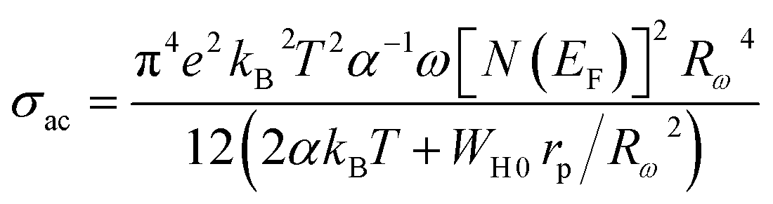 | (19) |
The equation below defines the hopping length Rω:
 | (20) |
The inverse localization length is denoted by the parameter α,  , β = 1/kBT and
  .
.
The following expression defines the parameter s within this approach:53
 | (21) |
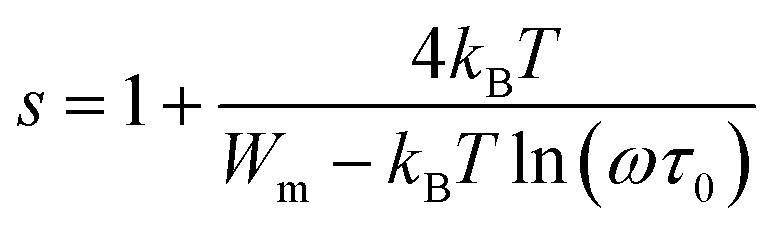
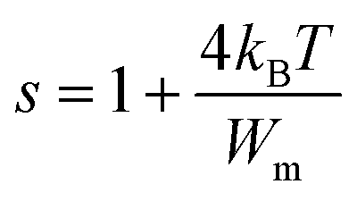
According to eqn (19), the theoretical calculations based on the OLPT model (shown in Fig. 10(a)) are consistent with the experimental measurements. The OLPT model parameters obtained from eqn (17) and (18) are listed in Tables 4 and 5. The values of parameter α fall within the same range as reported by Murawski et al.54 Moreover, the N(EF) values are reasonable for localized states. The frequency dependence of the parameter Rω (Cs2AgBiCl6) is shown in Fig. 10(b). It is interesting to note that the tunneling distances Rω (3.729–3.821 Å) are in close proximity to the interatomic distances Cs–Cl (3.810 Å) within Cs2AgBiCl6. These findings may indicate that the mobility of Cs+ cations facilitates AC conductivity through large polaron motion.55
 | ||
| Fig. 10 (a) Temperature dependence of the ln(σAC) at different frequencies. (b) Frequency-dependent of the parameter Rω (Å) for Cs2MBiCl6 (M = Cu, Ag). (c) Frequency-dependent of the parameters α (Å−1), N(EF) (eV−1 cm−3). | ||
| Frequency (Hz) | α (Å−1) | WHO (eV) | N (cm−3) | rp (Å) | Rω (Å) |
|---|---|---|---|---|---|
| 103 | 0.71 | 0.654 | 2.24 × 1025 | 1.309 | 3.821 |
| 104 | 0.80 | 0.606 | 3.78 × 1025 | 1.293 | 3.795 |
| 105 | 0.84 | 0.572 | 5.99 × 1025 | 1.276 | 3.764 |
| 106 | 0.86 | 0.511 | 8.36 × 1025 | 1.247 | 3.729 |
| Frequency (Hz) | εp (F m−1) | WH (eV) |
|---|---|---|
| 103 | 6.28 × 10⁻⁹ | 0.367 |
| 104 | 7.06 × 10⁻⁹ | 0.335 |
| 105 | 7.77 × 10⁻⁹ | 0.318 |
| 106 | 8.45 × 10⁻⁹ | 0.300 |
The parameter s is expressed as follows within the NSPT approach:54
 | (22) |
The activation energy for polaron transfer is denoted by Wm. KB represents the Boltzmann constant, and τ0 represents the characteristic relaxation time (approximately 10−13 s).
The following equation expresses the parameter s for large values of Wm/kBT:
 | (23) |
The value of Wm (corresponding to 0.146 eV) was obtained by curve fitting for Cs2CuBiCl6 (as shown in Fig. 9(d)). It should be noted that, in this approach, the value of Wm is independent of the intersite separation since the small polarons are confined in such a way that their cloud distortions do not interfere.17
The following equation expresses the AC conductivity within the NSPT approach.18
 | (24) |
 | (25) |
The AC conductivity is determined by the following equation in the NSPT approach, where N(EF) represents the density of states near the Fermi level, α−1 denotes the spatial extension of the polaron, and Rω refers to the tunneling distance. The variation of ln(σAC) with temperature is shown in Fig. 10(a). It is evident from this figure that the fit is in good agreement with the experimental measurements (Cs2CuBiCl6). Table 6 shows all NSPT model parameters, which were obtained from the fitting of the data points. It should be noted that the N(EF) values are reasonable for localized states.17 The frequency dependence of the parameters N(EF) and α are shown in Fig. 10(c), where it is observed that both parameters decrease as the frequency increases. This trend is consistent with previous reports.25 The corresponding values of the tunneling distance ‘Rω’ obtained from eqn (25) are presented in Table 6.
| Frequency (Hz) | α (Å−1) | N(EF) (eV−1 cm−3) | Rω (Å) |
|---|---|---|---|
| 103 | 0.74 | 8.09 × 1027 | 3.912 |
| 104 | 0.77 | 1.00 × 1028 | 3.909 |
| 105 | 0.81 | 1.27 × 1028 | 3.906 |
| 106 | 0.85 | 1.84 × 1028 | 3.903 |
Fig. 10(b) demonstrates the frequency dependence of Rω (Cs2CuBiCl6), indicating a decrease in the hopping distance with increasing frequency. This trend suggests that charge carriers move from long-distance to short-distance tunneling, which could account for the observed increase in N(EF) (∼1028 eV−1 cm−3) with frequency.18 It is noteworthy that the tunneling distances Rω (3.903–3.912 Å) are similar to the interatomic distances Cs–Cl (3.910 Å) within Cs2CuBiCl6. This observation implies that the mobility of Cs+ cations facilitates AC conductivity via a small polaron motion.55
As a part of this work, we investigated the electrical and optical characteristics of Cs2MBiCl6 (M = Ag, Cu). Based on the available literature,56,57 it has been observed that the CBM (conduction band minimum) in the Cs2AgBiCl6 compound primarily originated from the Cl-3p, Bi-6p, and Ag-5s orbitals, with a minor contribution from the Ag-4d orbital. Conversely, the VBM (valence band maximum) mainly consists of Ag-4d and Cl-3p orbitals, with a minimal contribution from the Bi-6s orbitals. In the case of Cs2CuBiCl6, which contains copper instead of silver, a significantly smaller indirect bandgap of 1.31 eV has been reported, with the CBM located at the Γ symmetry point and the VBM at the X point. According to the literature, the CBM in Cs2CuBiCl6 is predominantly composed of Cl-3p, Bi-6p, Cu-4s, and Cu-3d orbitals, while the VBM consists mainly of Cu-3d, Cl-3p, and Bi-6s orbitals. It is worth noting that despite both compounds having a cubic double perovskite phase, Cs2AgBiCl6 exhibits a considerably larger indirect bandgap energy of 2.92 eV compared to Cs2CuBiCl6 (1.31 eV). This variation in the bandgap energy between Cs2MBiCl6 (where M = Ag, Cu) can be attributed to the change in the metal component, as the semiconductor characteristics are closely linked to the structural arrangement.
Furthermore, the Nyquist plots and the frequency-variation (AC) conductivity of Cs2MBiCl6 (M = Ag, Cu) at 340 K, shown in Fig. 11, show that the larger conductivity is noted in Cs2CuBiCl6. The electrical and optical (bandgap) characteristics are related to the structure of [BiCl6]3− and [MCl6]5− (M = Ag, Cu) octahedra and their coupling. This can be explained by the structural difference between these two compounds, precisely at the level of the anion [MCl6]5− (M = Ag, Cu). Due to the Jahn–Teller effect, the copper coordination octahedra in Cs2CuBiCl6 are usually distorted, thus changing the energetics of the different bonds in the crystal structure. We can then think that the delocalization of charge carriers within the Cs2CuBiCl6 compound is easier, which favors the increase in their AC conductivity.
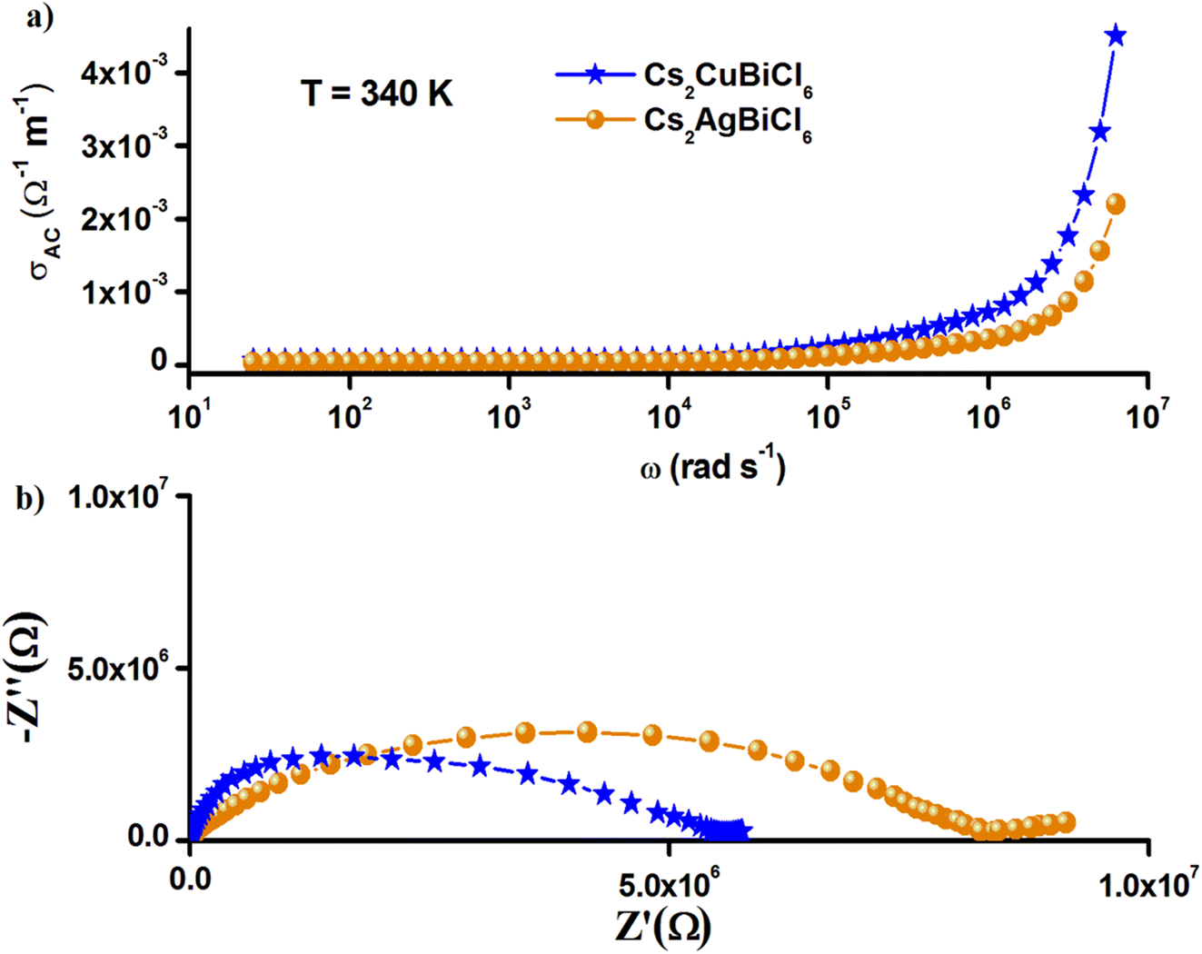 | ||
| Fig. 11 (a) Nyquist diagram and (b) AC conductivity of Cs2MBiCl6 (M = Cu, Ag) at 340 K. | ||
4. Conclusions
To summarize, the slow evaporation solution growth method was used to synthesize Cs2MBiCl6 (M = Ag, Cu) double perovskites. The X-ray diffraction pattern confirmed that the compounds have a cubic symmetry. The indirect bandgap energies were determined to be 1.31 eV and 2.92 eV for Cs2CuBiCl6 and Cs2AgBiCl6, respectively. The double-layer Maxwell–Wagner effect has been proposed as the explanation for the significant change in relative permittivity in Cs2MBiCl6 (M = Ag, Cu). The free charge and space-charge conductivity were evaluated using the modified Cole–Cole plot and were found to increase as the temperature increased. The analysis of the Nyquist curves supported the presence of grain, grain boundaries, and electrode processes. The KWW model was used to evaluate the asymmetric plots of the modulus formalism for both materials. The non-Debye behavior of M′′(ω) decreased with increasing temperature. The activation energy was calculated from DC conductivity and the modulus spectra for each material, which showed similar values. This suggests that the conduction mechanism and the relaxation behavior are similar in Cs2MBiCl6 (M = Ag, Cu). The AC conductivity of Cs2MBiCl6 (M = Ag, Cu) was investigated using Jonscher's power law. The OLPT and NSPT models were used to interpret the conduction mechanisms for Cs2AgBiCl6 and Cs2CuBiCl6, respectively, based on Elliot's theory. The results from these models suggest that the AC conductivity in Cs2MBiCl6 (M = Ag, Cu) is facilitated by the mobility of Cs+ cations through the tunneling mechanism. The favorable energy band gap, conductivity, relaxation time, and dielectric constant of Cs2MBiCl6 (M = Ag, Cu) make it a promising material for energy-harvesting systems.Conflicts of interest
There are no conflicts to declare.Acknowledgements
We are thankful for the financial support provided by the Ministry of Higher Education and Scientific Research of Tunisia.References
- E. Akman, T. Ozturk, W. Xiang, F. Sadegh, D. Prochowicz, M. M. Tavakoli, P. Yadav, M. Yilmaz and S. Akin, Energy Environ. Sci., 2023, 16(2), 372 RSC.
- T. Öztürk, E. Akman, A. E. Shalan and S. Akin, Nano Energy, 2021, 87, 106157 CrossRef.
- W. Xiang, Z. Wang, D. J. Kubicki, W. Tress, J. Luo, D. Prochowicz, S. Akin, L. Emsley, J. Zhou, G. Dietler, M. Grätzel and A. Hagfeldt, Joule, 2019, 3(1), 205 CrossRef CAS.
- X. Luo, R. Lai, Y. Li, Y. Han, G. Liang, X. Liu, T. Ding, J. Wang and K. Wu, J. Am. Chem. Soc., 2019, 141, 4186 CrossRef CAS PubMed.
- K. R. Pradeep and R. Viswanatha, Mater. Res. Bull., 2021, 141, 5 CrossRef.
- Y. Wang, Y. Teng, P. Lu, X. Shen, P. Jia, M. Lu, Z. Shi, B. Dong, W. W. Yu and Y. Zhang, Adv. Funct. Mater., 2020, 30, 1910140 CrossRef CAS.
- J. Ghosh and P. K. Giri, Mater. Res. Bull., 2021, 139, 10 CrossRef.
- Rahul, P. K. Singh, R. Singh, V. Singh, B. Bhattacharya and Z. H. Khan, Mater. Res. Bull., 2018, 97, 572 CrossRef CAS.
- F. Liu, C. Ding, Y. Zhang, T. S. Ripolles, T. Kamisaka, T. Toyoda, S. Hayase, T. Minemoto, K. Yoshino, S. Dai, M. Yanagida, H. Noguchi and Q. Shen, J. Am. Chem. Soc., 2017, 139, 16708 CrossRef CAS PubMed.
- C. Wang, Y. Liu, Y. Guo, L. Ma, Y. Liu, C. Zhou, X. Yu and G. Zhao, Chem. Eng. J., 2020, 397, 125367 CrossRef CAS.
- J. Luo, X. Wang, S. Li, J. Liu, Y. Guo, G. Niu, L. Yao, Y. Fu, L. Gao, Q. Dong, C. Zhao, M. Leng, F. Ma, W. Liang, L. Wang, S. Jin, J. Han, L. Zhang, J. Etheridge, J. Wang, Y. Yan, E. H. Sargent and J. Tang, Nature, 2018, 563, 541 CrossRef CAS PubMed.
- K. Kundu, P. Dutta, P. Acharyya and K. Biswas, Mater. Res. Bull., 2021, 140, 10 CrossRef.
- N. Daem, J. Dewalque, F. Lang, A. Maho, G. Spronck, C. Henrist, P. Colson, S. D. Stranks and R. Cloots, Sol. RRL, 2021, 5(9), 2100422 CrossRef CAS.
- N. Chen, T. Cai, W. Li, K. Hills-Kimball, H. Yang, M. Que, Y. Nagaoka, Z. Liu, D. Yang, A. Dong, C. Y. Xu, R. Zia and O. Chen, ACS Appl. Mater. Interfaces, 2019, 11, 16855 CrossRef CAS PubMed.
- L. Li, H. Shao, X. Wu, W. Chen, J. Zhu, B. Dong, L. Xu, W. Xu, J. Hu, M. Zhou, Y. Ji, H. Song and X. Bai, Mater. Res. Bull., 2022, 147, 111645 CrossRef CAS.
- J. Wu, Z. Zhao and Y. Zhou, Sci. Rep., 2022, 12, 935 CrossRef CAS PubMed.
- M. Ben bechir and M. H. Dhaou, RSC Adv., 2021, 11, 21767 RSC.
- M. Ben bechir and M. H. Dhaou, Mater. Res. Bull., 2021, 114, 111473 CrossRef.
- T. Paul and A. Ghosh, J. Appl. Phys., 2017, 121, 135106 CrossRef.
- E. T. McClure, M. R. Ball, W. Windl and P. M. Woodward, Chem. Mater., 2016, 28, 1348 CrossRef CAS.
- H.-J. Feng, W. Deng, K. Yang, J. Huang and X. C. Zeng, J. Phys. Chem. C, 2017, 121, 4471 CrossRef CAS.
- M. Wang, P. Zeng, Z. Wang and M. Liu, Adv. Sci., 2020, 7(11), 1903662 CrossRef CAS PubMed.
- N. K. Tailor, J. Ghosh, M. A. Afroz, S. L. Bennett, M. Chatterjee, P. J. Sellin and S. Satapathi, ACS Appl. Electron. Mater., 2022, 4(9), 4530 CrossRef CAS.
- J. Zhou, Z. Xia, M. S. Molokeev, X. Zhang, D. Peng and Q. Liu, J. Mater. Chem. A, 2017, 5(29), 15031 RSC.
- D. Wu, Y. Tao, Y. Huang, B. Huo, X. Zhao, J. Yang, X. Jiang, M. Ceccarelli, F. Dong and X. Tasng, J. Catal., 2021, 397, 27 CrossRef CAS.
- R. Kalthoum, M. Ben Bechir and A. Ben Rhaiem, Phys. E, 2020, 124, 114235 CrossRef CAS.
- I. Romdhane, M. Ben Bechir and M. H. Dhaou, Phys. E, 2022, 136, 115008 CrossRef CAS.
- S. M. H. Qaid, B. A. Al-Asbahi, H. M. Ghaithan, M. S. AlSalhi and A. S. Al dwayyan, J. Colloid Interface Sci., 2020, 563, 426 CrossRef CAS PubMed.
- J. Tauc, in Amorphous and Liquid Semiconductors, ed. J. Tauc, Plenum Press, London and New York, 1974 Search PubMed.
- S. K. Gagandeep, B. S. Lark and H. S. Sahota, Nucl. Sci. Eng., 2000, 134, 208 CrossRef.
- G. S. Shahane, B. M. More, C. B. Rotti and L. P. Deshmukh, Mater. Chem. Phys., 1997, 47, 263 CrossRef CAS.
- D. Bhattacharya, S. Chaudhuri and A. K. Pal, Vacuum, 1992, 43, 313 CrossRef.
- D. K. Pattanayak, R. K. Parida, N. C. Nayak, A. B. Panda and B. N. Parida, J. Mater. Sci.: Mater. Electron., 2018, 29, 6215 CrossRef CAS.
- P. Maji, S. Chatterjee and S. Das, Ceram. Int., 2015, 45, 6012 CrossRef.
- D. K. Pradhan, P. Misra, V. S. Puli, S. Sahoo, D. K. Pradhan and R. S. Katiyar, J. Appl. Phys., 2014, 115, 243904 CrossRef.
- A. Ray, A. Roy, S. De, S. Chatterjee and S. Das, J. Appl. Phys., 2018, 123, 104102 CrossRef.
- Y. Mateyshina, A. Slobodyuk, V. Kavun and N. Uvarov, Solid State Ionics, 2018, 324, 196 CrossRef CAS.
- A. Dhara, S. Sain, S. Das and S. K. Pradhan, Mater. Res. Bull., 2018, 97, 169 CrossRef CAS.
- T. Wang, J. Hu, H. Yang, L. Jin, X. Wei, C. Li, F. Yan and Y. Lin, J. Appl. Phys., 2017, 121, 084103 CrossRef.
- C. R. Cena, A. K. Behera and B. Behera, J. Adv. Ceram., 2016, 5, 84 CrossRef CAS.
- C. G. Koops, Phys. Rev., 1951, 83, 121 CrossRef CAS.
- M. Ahmad, M. A. Rafiq, K. Rasool, Z. Imran and M. M. Hasan, J. Appl. Phys., 2013, 113, 043704 CrossRef.
- P. Thongbai, S. Tangwancharoen, T. Yamwong and S. Maensiri, J. Phys.: Condens. Matter, 2008, 20, 395227 CrossRef.
- M. Ben Bechir, K. Karoui, M. Tabellout, K. Guidara and A. Ben Rhaiem, Phase Transitions, 2018, 91(8), 901 CrossRef CAS.
- D. K. Rana, S. K. Singh, S. K. Kundu, S. Roy, S. Angappane and S. Basu, New J. Chem., 2019, 43, 3128 RSC.
- P. Sengupta, P. Sadhukhan, A. Ray, R. Ray, S. Bhattacharyya and S. Das, Appl. Phys., 2020, 127, 204103 CAS.
- B. E. Jun, H. K. Kim, Y. H. Hwang, B. C. Choi, J. H. Jeong, J. S. Bae and C. H. Kim, J. Korean Phys. Soc., 2006, 49, 2408 CAS.
- D. K. Pradhan, P. Misra, V. S. Puli, S. Sahoo, D. K. Pradhan and R. S. Katiyar, J. Appl. Phys., 2014, 115, 243904 CrossRef.
- N. Vol, Nature, 1977, 267, 673 CrossRef.
- M. Ben bechir and A. Ben Rhaiem, Phys. E, 2020, 120, 114032 CrossRef CAS.
- M. Ben bechir and A. Ben Rhaiem, Phys. E, 2021, 130, 114686 CrossRef CAS.
- M. Ben Bechir, K. Karoui, M. Tabellout, K. Guidara and A. Ben Rhaiem, J. Appl. Phys., 2014, 115, 203712 CrossRef.
- M. Ben bechir and A. Ben Rhaiem, J. Solid State Chem., 2021, 296, 122021 CrossRef CAS.
- M. Ben Bechir, K. Karoui, M. Tabellout, K. Guidara and A. Ben Rhaiem, J. Appl. Phys., 2014, 115, 153708 CrossRef.
- The Materials Project, Materials Data on Cs2CuBiCl6 by Materials Project, United States, 2020, DOI:10.17188/1757355.
- M. R. Filip, S. a. J. Hillman, A. A. Haghighirad, H. J. Snaith and F. Giustino, J. Phys. Chem. Lett., 2016, 7(13), 2579–2585 CrossRef CAS PubMed.
- W. Shi, T. Cai, Z. Wang and O. Chen, J. Chem. Phys., 2020, 153(14), 141101 CrossRef CAS PubMed.
| This journal is © The Royal Society of Chemistry 2023 |