
 Open Access Article
 This Open Access Article is licensed under a Creative Commons Attribution-Non Commercial 3.0 Unported Licence
Harnessing the potential of CsPbBr3-based perovskite solar cells using efficient charge transport materials and global optimization
M. Khalid Hossain *a,
Sagar Bhattaraib,
A. A. Arnabc,
Mustafa K. A. Mohammedd,
Rahul Pandeye,
Md Hasan Alif,
Md. Ferdous Rahmanf,
Md. Rasidul Islamg,
D. P. Samajdarh,
Jaya Madane,
H. Bencherifi,
D. K. Dwivedij and
Mongi Amamik
*a,
Sagar Bhattaraib,
A. A. Arnabc,
Mustafa K. A. Mohammedd,
Rahul Pandeye,
Md Hasan Alif,
Md. Ferdous Rahmanf,
Md. Rasidul Islamg,
D. P. Samajdarh,
Jaya Madane,
H. Bencherifi,
D. K. Dwivedij and
Mongi Amamik
aInstitute of Electronics, Atomic Energy Research Establishment, Bangladesh Atomic Energy Commission, Dhaka 1349, Bangladesh. E-mail: khalid.baec@gmail.com; khalid@kyudai.jp
bDepartment of Physics, Arunachal University of Studies, Namsai, 792103, Arunachal Pradesh, India
cDepartment of Electrical & Electronic Engineering, Ahsanullah University of Science and Technology, Dhaka 1208, Bangladesh
dUniversity of Warith Al-Anbiyaa, 56001 Karbala, Iraq
eVLSI Centre of Excellence, Chitkara University Institute of Engineering and Technology, Chitkara University, Punjab 140401, India
fAdvanced Energy Materials and Solar Cell Research Laboratory, Department of Electrical and Electronic Engineering, Begum Rokeya University, Rangpur 5400, Bangladesh
gDepartment of Electrical and Electronic Engineering, Bangamata Sheikh Fojilatunnesa Mujib Science & Technology University, Jamalpur 2012, Bangladesh
hDepartment of ECE, Indian Institute of Information Technology, Design & Manufacturing, Madhya Pradesh 482005, India
iLEREESI, Higher National School of Renewable Energies, Environment and Sustainable Development, Batna 05078, Algeria
jDepartment of Physics and Material Science, Madan Mohan Malaviya University of Technology, Gorakhpur-273010, U.P., India
kDepartment of Chemistry, College of Sciences, King Khalid University, P.O. Box 9004, Abha, Saudi Arabia
First published on 12th July 2023
Abstract
Perovskite solar cells (PSCs) have become a possible alternative to traditional photovoltaic devices for their high performance, low cost, and ease of fabrication. Here in this study, the SCAPS-1D simulator numerically simulates and optimizes CsPbBr3-based PSCs under the optimum illumination situation. We explore the impact of different back metal contacts (BMCs), including Cu, Ag, Fe, C, Au, W, Pt, Se, Ni, and Pd combined with the TiO2 electron transport layer (ETL) and CFTS hole transport layer (HTL), on the performance of the devices. After optimization, the ITO/TiO2/CsPbBr3/CFTS/Ni structure showed a maximum power conversion efficiency (PCE or η) of 13.86%, with Ni as a more cost-effective alternative to Au. After the optimization of the BMC the rest of the investigation is conducted both with and without HTL mode. We investigate the impact of changing the thickness and the comparison with acceptor and defect densities (with and without HTL) of the CsPbBr3 perovskite absorber layer on the PSC performance. Finally, we optimized the thickness, charge carrier densities, and defect densities of the absorber, ETL, and HTL, along with the interfacial defect densities at HTL/absorber and absorber/ETL interfaces to improve the PCE of the device; and the effect of variation of these parameters is also investigated both with and without HTL connected. The final optimized configuration achieved a VOC of 0.87 V, JSC of 27.57 mA cm−2, FF of 85.93%, and PCE of 20.73%. To further investigate the performance of the optimized device, we explore the impact of the temperature, shunt resistance, series resistance, capacitance, generation rate, recombination rate, Mott–Schottky, JV, and QE features of both with and without HTL connected. The optimized device offers the best thermal stability at a temperature of 300 K. Our study highlights the potential of CsPbBr3-based PSCs and provides valuable insights for their optimization and future development.
1 Introduction
In recent years, the exponential increase in demand for conventional energy sources, coupled with the rapid depletion of fossil fuels due to extensive industrialization, has led to serious environmental and economic concerns.1–5 In response, photovoltaic (PV) solar cells appear to be one of the most promising solutions for sustainable energy production, offering both environmental benefits and cost-effectiveness.6–8 Among the various types of PV solar cells, thin film solar cells (TFSCs) have gained widespread consideration due to their fast growth and potential for high performance.9–14 However, the efficiency of TFSCs is strongly influenced by the choice of semiconductor materials and growth methods employed. Despite incremental gains in efficiency since the invention of the first modern silicon solar cell in 1954, significant progress has been made, with modules developed by 2010 capable of converting up to 18% of solar energy into electricity.15The TFSCs have gained significant consideration in recent years, particularly organic-inorganic metal halide perovskite solar cells, owing to their remarkable optoelectronic features, such as improved absorption coefficients, customizable band gaps, longer electron and hole diffusion lengths, low cost, efficient charge separation, and solution processability.16–19 Perovskite compounds with the chemical formula PQX3 (XIIP2+VIQ4+X32−), consisting of an organic cation P (e.g., methylammonium or formamidinium), a divalent metal B (e.g., Pb or Sn), and a halide X (e.g., Br or I),20 are of particular interest for the lower cost and easier manufacturing.21,22 The efficiency of PSCs has increased dramatically, from an initial maximum PCE or η of 3.8% in 2009 to a remarkable PCE of 25.2% in 2019,23,24 with current overall PCE on PSCs reaching up to 23%,25 similar to CIGS based solar cells and commercialized silicon-based solar cells.26 Regardless of their superior performance, the instability of PSCs, caused by the presence of organic elements, has been a major concern. To address this issue, researchers have investigated the use of alternative inorganic ions (such as Cs+) with organic ions. In 2012, the very first Cs-based perovskite i.e. CsSnI3 with Schottky solar cells was reported, with a PCE of 0.88 percent.27 There onwards extensive work has been going on to enhance the performance of the CsPbI3-based PSC device. Although CsPbI3 has an appropriate energy band gap of 1.73 eV and an efficiency of 13.21%,28 its phase stability at ambient temperature is poor, degrading rapidly to a non-perovskite yellow phase δ-CsPbI3.28,29 Recently, researchers have focused on developing dual-halide inorganic perovskite CsPbIxBr3−x to enhance the stability as well as the efficiency of all-inorganic perovskite. The best efficiency of any inorganic perovskite solar cell recorded so far is achieved by the SnO2/ZnO bi-layer electron transport layer-based CsPbI2Br PSC with a high PCE of 14.6%.30,31 However, the overall sustainability of the dual-halide perovskite remains inadequate. Although most efficient CsPbBr3 PSC described are mesostructured, requiring a high-temperature treatment for the electron transport layers,32 Liang et al. have produced a hole-conductor-free PSC with a compact TiO2/m-TiO2/CsPbBr3/carbon structure, that achieved a PCE of 6.7%.33
In the field of PSCs, carrier transport materials, or electron transport layers (ETLs), play a crucial role in achieving high efficiency.34–38 Titanium dioxide (TiO2) is one of the most commonly used ETLs due to its popularity and ease of processing.39 However, it's high resistance and limited carrier mobility compared to the perovskite layer can limit the device's performance.40 To address this, TiO2 must be doped to increase its energy bands and conductivity.41 Additionally, while high efficiency has been achieved, there is still a need to develop PSCs using earth-abundant, nontoxic, and affordable materials. Several compounds, including FeS2, Bi2S3, Cu2S, and SnS, have been studied in this regard.42–44 Quaternary chalcogenides, specifically Cu2ZnSn(S, Se)4 known as CZTSSe, have shown promise in this area.45 Various vacuum and non-vacuum-based techniques for producing Cu2FeSnS4 (CFTS), a p-type material with an acceptable band gap (1.28–1.50 eV) and high optical absorption coefficients (>104 cm−1), have also been established.46,47 CFTS is composed of abundant and affordable elements that are relatively non-toxic. Replacing Zn with Fe in CZTS thin films further lowers its optical energy band gap and enhances conductivity, leading to improved solar-to-electrical conversion efficiency.48
This research is the extension of our previous study49 where we studied about nine HTLs and six ETL-associated 54 combinations of PSCs configuration where the best six structures performance studies are conducted. In this study, we optimized the optoelectronic parameters of CsPbBr3-based PSCs utilizing SCAPS-1D simulation software. This paper is divided into four different sections, 1–4. Introduction Section 1 is followed by device modeling Section 2 where a detailed description of simulation methodology is provided along with the device and material parameters considered during simulations. Results are reported in Section 3, which is started by optimizing the BMC of the ITO/TiO2/CsPbBr3/CFTS/Au solar cell device structure. We further investigated the impact of absorber layer thickness, charge carrier density, as well as defect density with and without HTL-connected conditions. Additionally, we optimized the thickness of the ETL and HTL, charge carrier density, and interface defect density in both with and without HTL-connected modes. Finally, we observed the optimized device's quantum efficiency, J–V characteristics, generation recombination rate, capacitance, and Mott–Schottky characteristics in both HTL and non-HTL modes. The results of the finding are concluded in the conclusion Section 4. Our study provides a cost-effective and unique approach to designing and constructing high-performance PSCs.
2 Device modeling
2.1 Simulation
In the present study, SCAPS-1D simulation software50–59 is used to study the CsPbBr3-based solar cell configuration. The simulator program employs 3-coupled differential equations: i.e. Poisson's equation (eqn (1)), the equation of continuity for electrons (eqn (2)), and the equation of continuity for holes (eqn (3)). These equations are shown below.60
 | (1) |
 | (2) |
 | (3) |
2.2 Device structure
In this research optimization of optoelectronic parameters of CsPbBr3-based PSC is mainly conducted where TiO2 is taken as ETL, CFTS is taken as HTL, and Au as BMC initially. Whereas, the optoelectronic parameters of different materials are taken from previous studies which are listed in Tables 1 and 2. To find out the optimized structure for different combinations of ETL and HTL is performed through SCAPS-1D to determine the most efficient structure. From Table 1, it is seen that TiO2 is taken as ETL and their optoelectronic parameters are also included in Table 1. Also from Table 1, it is seen that CFTS is taken as HTL and their optoelectronic parameters are also included. In Table 2, the interface layer's parameters are listed. In addition, CsPbBr3 absorber layer optoelectronic parameters are also included in Table 1 and sequentially simulate different structure configurations and evaluate the photovoltaic features like open-circuit voltage (VOC), short circuit current density (JSC), fill Factor (FF), and PCE to find out the primarily optimized PSC's configuration before the variation of parameters. After many trials and errors, ITO/TiO2/CsPbBr3/CFTS/Au structure finds out to be an efficient primary structure. To increase the efficiency, many variations of optoelectronic parameters are also done. Fig. 1(a) gives an illustrative observation of the working strategy of this study. Here in Fig. 1(a), it is seen in the middle there is light-absorbing material as CsPbBr3 and it is sandwiched between TiO2 ETL and CFTS HTL. Fig. 1(b) gives an idea about the energy band diagram of the proposed solar cell structure. Where on the x-axis is the thickness and on the y-axis energy (eV), HTL's valence band Fermi-level is higher than that of the CsPbBr3 absorber layer.| Parameters | TCO | TiO2 | CFTS | CsPbBr3 |
|---|---|---|---|---|
| a In this study CsPbBr3 absorber layer's thickness makes a constant of 800 nm primarily also the constant defect density of 1 × 1015 cm−3 at the initial condition. After the optimization process begins then variation will perform. | ||||
| Thickness (μm) | 0.5 | 0.03 | 0.1 | 0.8a |
| Band gap, Eg (eV) | 3.5 | 3.2 | 1.3 | 2.3 |
| Electron affinity, χ (eV) | 4 | 3.9 | 3.3 | 3.6 |
| Dielectric permittivity (relative), εr | 9 | 9 | 9 | 6.5 |
| CB effective density of states, NC (cm−3) | 2.2 × 10¹⁸ | 2 × 10¹⁸ | 2.2 × 10¹⁸ | 4.94 × 10¹⁷ |
| VB effective density of states, NV (cm−3) | 1.8 × 10¹⁹ | 1.8 × 10¹⁹ | 1.8 × 10¹⁹ | 8.47 × 10¹⁸ |
| Electron mobility, μn (cm2 V−1 s−1) | 20 | 20 | 21.98 | 4500 |
| Hole mobility, μh (cm2 V−1 s−1) | 10 | 10 | 21.98 | 4500 |
| Shallow uniform acceptor density, NA (cm−3) | 0 | 0 | 1 × 10¹⁸ | 0 |
| Shallow uniform donor density, ND (cm−3) | 1 × 10²¹ | 9 × 10¹⁶ | 0 | 1 × 10¹⁵ |
| Defect density, Nt (cm−3) | 1 × 10¹⁵a | 1 × 10¹⁵a | 1 × 10¹⁵a | 1 × 10¹⁵a |
| Interface | Defect type | Capture cross section: electrons/holes (cm2) | Energetic distribution | Reference for defect energy level | Total density (cm−2) (integrated over all energies) |
|---|---|---|---|---|---|
| ETL/CsPbBr3 | Neutral | 1.0 × 10⁻¹⁷ | Single | Above the VB maximum | 1.0 × 10¹⁰ |
| 1.0 × 10⁻¹⁸ | |||||
| CsPbBr3/HTL | Neutral | 1.0 × 10⁻¹⁸ | Single | Above the VB maximum | 1.0 × 10¹⁰ |
| 1.0 × 10⁻¹⁹ |
 | ||
| Fig. 1 (a) Schematic structure, and (b) energy band diagram of CsPbBr3-based PSC. | ||
3 Result and discussion
3.1 BMC optimization
In this section, we emphasized the optimization of the BMC of the ITO/TiO2/CsPbBr3/CFTS/BMC solar cell structure. To increase the output parameters of the PSC, various BMC's work function variation is also done. Metals are arranged according to their work function values. It is widely known that when the work-function of the contact metal declines, the devices' shunt resistance and performance also fall. Specifically, when using Ag as BMC the performance is lower compared to the rest of the metals. Besides the low work function, Ag present also has a serious stability problem. The use of Cu and Fe as BMCs with high work function leads to favorable band bending at the perovskite-HTM-BMC interfaces, providing an efficient barrier to electron transfer from perovskite to metal and to high RSH which reduces the alternative current path created previously by the low RSH value. Besides, these metals form low interfacial resistance with the HTM. However, the solar cell performance remains almost constant with back contact work function higher than that of the aforementioned BMCs. This is due to the fact that a further rise in the work function enhances RSH and remove completely the alternate current route for the light-generated current. The decline of reverse saturation current causes a higher value of FF for a low work function. Finally, Ni, as a back contact seems to be more efficient because it is cost-effective, and using Ni as a back contact, the solar cell configuration seems to be more efficient than the others. Finally, the optimized solar cell structure is ITO/TiO2/CsPbBr3/CFTS/Ni, whose performance parameters are VOC nearly 0.890 V, JSC nearly 17.98 mA cm−2, FF nearly 86.59%, while an improved PCE of 13.86% (Table 3).| BMC | Work function61 (eV) | VOC (V) | JSC (mA cm−2) | FF (%) | PCE (%) |
|---|---|---|---|---|---|
| Ag | 4.26 | 0.85 | 13.11 | 85.95 | 9.57 |
| Cu | 4.65 | 0.87 | 16.25 | 86.27 | 12.22 |
| Fe | 4.81 | 0.89 | 17.97 | 86.59 | 13.85 |
| C | 5 | 0.89 | 17.98 | 86.59 | 13.86 |
| Au | 5.1 | 0.89 | 17.98 | 86.59 | 13.86 |
| W | 5.22 | 0.89 | 17.98 | 86.59 | 13.86 |
| Ni | 5.5 | 0.89 | 17.98 | 86.59 | 13.86 |
| Pd | 5.6 | 0.89 | 17.98 | 86.59 | 13.86 |
| Pt | 5.7 | 0.89 | 17.98 | 86.59 | 13.86 |
| Se | 5.9 | 0.89 | 17.98 | 86.59 | 13.86 |
For the proper collection of holes via the rear contact, an ohmic contact must be created.62 The simulation is firstly done with Au as a back contact, but due to the adjustment of the back contact, there are some significant changes observed in performance parameters in the energy band diagram because there exists a Schottky barrier.
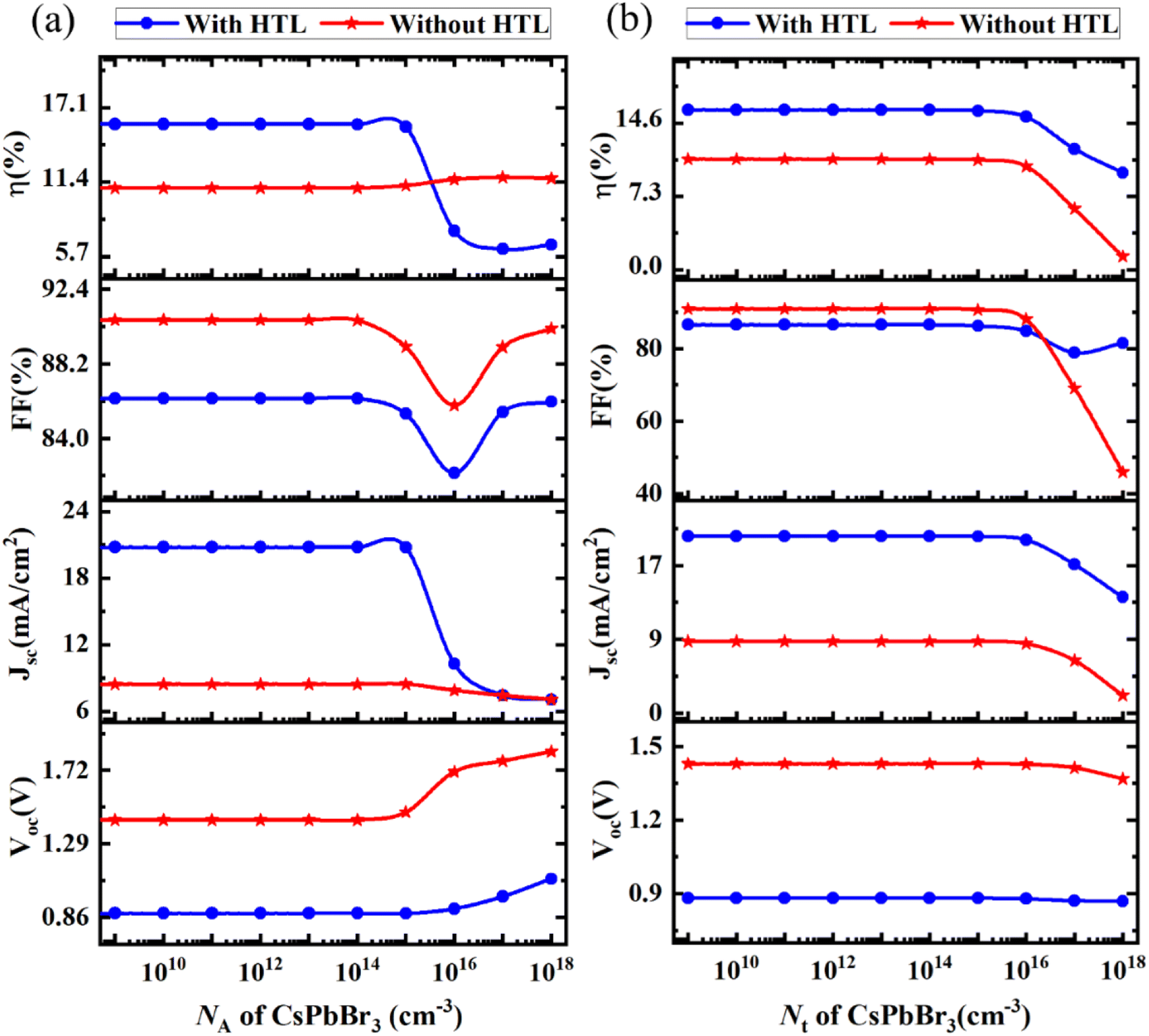
3.2 Combined influence of absorber thickness and the acceptor density
In this section, the impact of changing absorber layer thickness with absorber acceptor density variation simultaneously on TiO2 as ETL and CFTS as HTL and CsPbBr3 as absorber-based PSC's performance is observed through contour mapping in both HTL and without HTL connected mode. According to Fig. 2, the case without HTL connected structure shows the highest VOC which is 1.82 V. This increase is mainly attributed to both HTL-related series resistance and eliminated interface traps. Similarly, in the case of higher NA conditions and also absorber thickness increasing may increase the VOC. However, JSC shows differences, as compared to VOC, here with HTL connected structure, shows the highest JSC of 18.20 mA cm−2 in case of both high value of absorber thickness and NA condition, but NA has limitation up to 7 × 1017 cm−3 FF shows a 90.9% value in the case of without HTL connected mode and the parameters nature is exactly as similar as JSC's. However, the case of PCE with HTL connected structure shows the highest PCE which is 14% when the absorber thickness varies from 0.3 μm to 1.3 μm.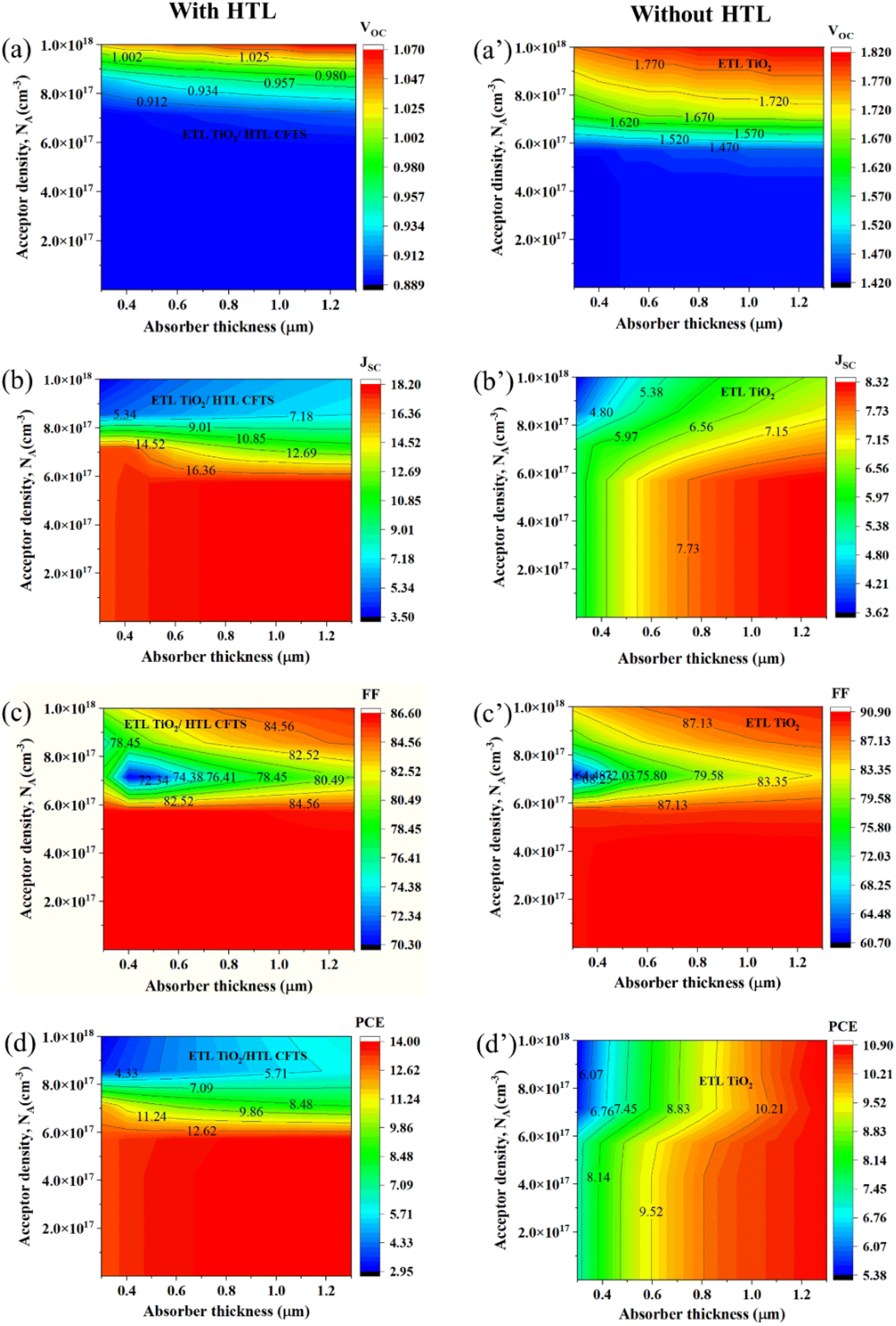 | ||
| Fig. 2 Contour mapping of performance parameters when ETL as TiO2. (a)–(d) with HTL, and (a′)–(d′) without HTL. | ||
The presence of HTL and the associated HTL/absorber interface can be a source of charge carrier recombination, which can reduce the VOC. In HTL-free devices, the charge carriers are transported directly from the perovskite layer to the anode, which reduces the opportunity for recombination. In addition, the carrier mobility in the HTL is typically lower than the carrier mobility in the perovskite layer. This means that the holes in the HTL can move more slowly, which can reduce the VOC. In HTL-free devices, the holes can move more quickly through the perovskite layer, which increases the VOC.
3.3 Combined impact of absorber thickness with defect density
The impact of changing the thickness of the absorber and defect density on solar cell outputs is discussed in this section. Where TiO2 is taken as well as the performance associated with ETL and CFTS as HTL. Both HTL and without HTL-Associated Mode (HTL-AM) performance are evaluated in this section. Fig. 3 shows the optimized solar cell performances where a higher VOC of 0.886 V is achieved in the case of HTL-AM when the thickness of the absorber ranges from 0.3 μm to 1.3 μm, and Nt ranges from 1 × 1011 cm−3 to 1 × 1018 cm−3. Where without HTL-AM shows a VOC of 1.43 V when the thickness of the absorber ranges from 0.3 μm to 1.3 μm regardless of Nt. The case of JSC with HTL-AM shows a JSC of 18.10 mA cm2; whereas without HTL-AM shows 8.31 mA cm−2 of JSC. But with HTL-AM shows 86.30% of FF when Nt ranges from 1 × 10¹¹ to 1 × 1018 cm−3, respectively. Whereas without HTL-AM shows 90.8% of FF when the thickness of the absorber ranges from 0.5 μm to 0.9 μm. Finally, HTL-AM shows 13.60% of PCE while the thickness of the absorber ranges from 0.8 to 1.2 μm whereas without HTL-AM shows 10.63% of PCE when the thickness of the absorber is greater than 1 μm as depicted in Fig. 3.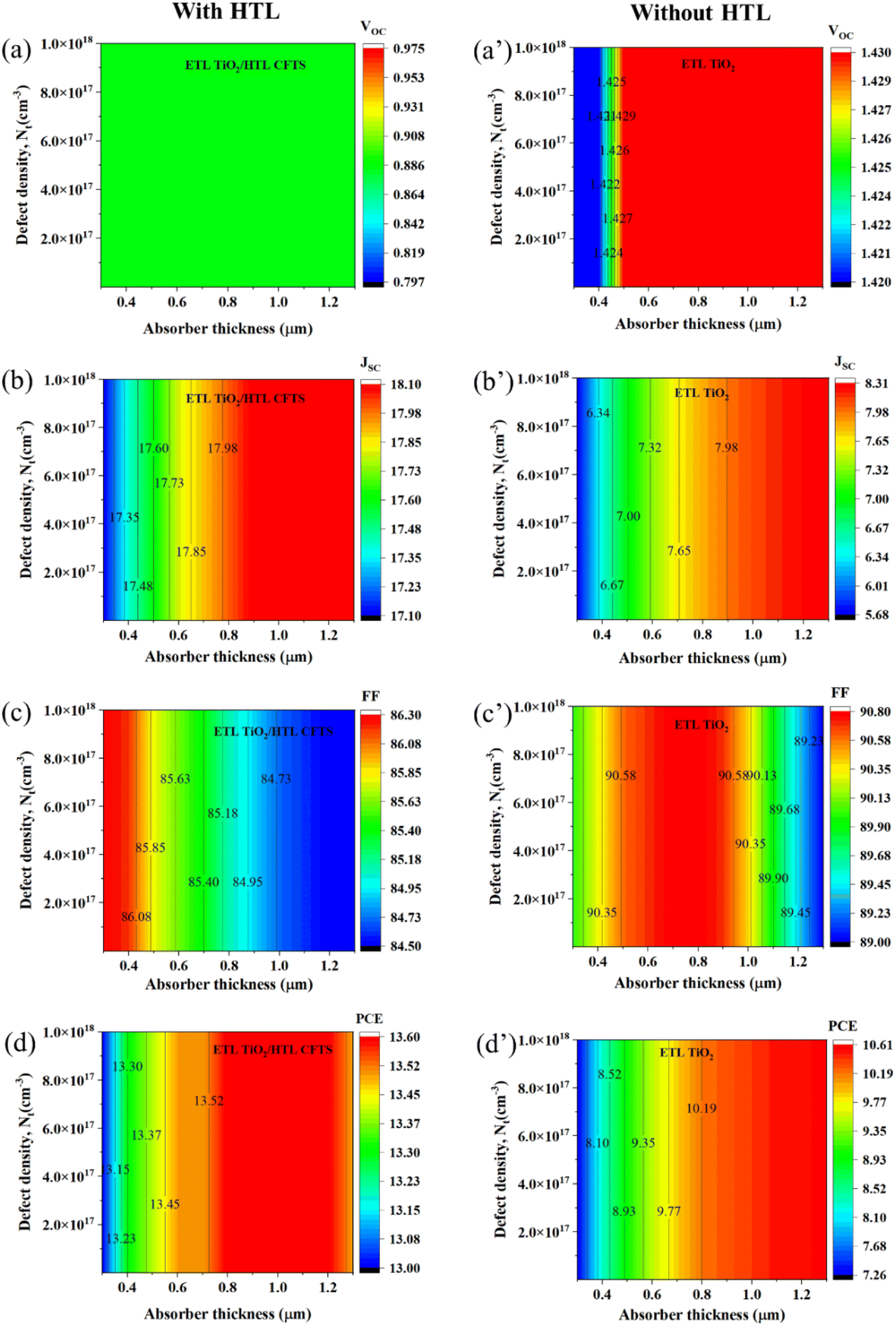 | ||
| Fig. 3 Contour mapping of performance parameters using TiO2 as ETL. (a)–(d) with HTL, and (a′)–(d′) without HTL. | ||
3.4 Optimization of absorber, ETL and HTL thickness
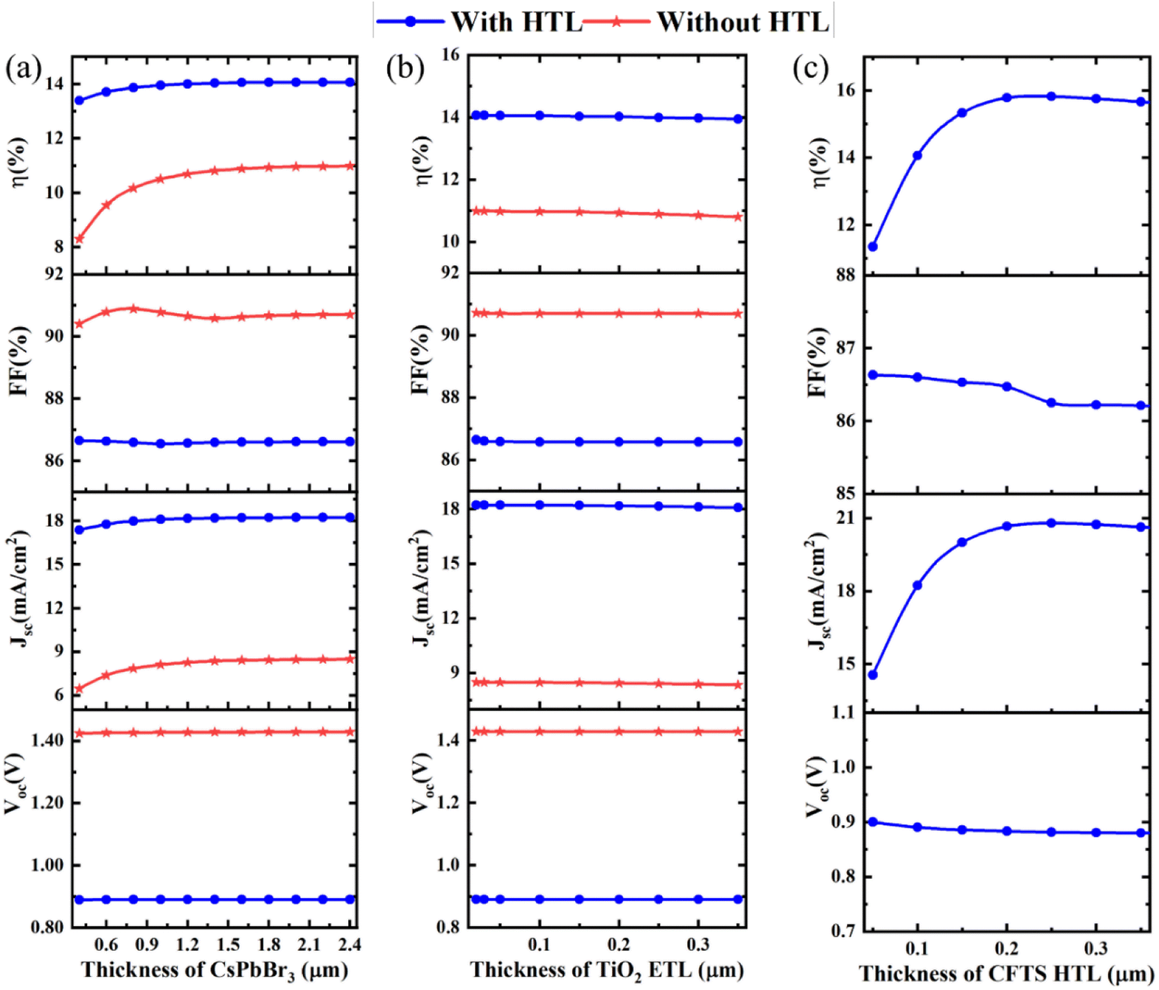 | ||
| Fig. 4 Thickness variation of (a) CsPbBr3, (b) TiO2, (c) CFTS. | ||
As the photon collection capacity rises with the enhancement of the absorber layer thickness, the rate of charge carrier creation also increases that's why VOC increases.46 Also from Fig. 4(a), it can be seen that JSC also enhances with the increase of thickness of the absorber. Because the spectral sensitivity at higher wavelengths increases with an increase in the thickness of the absorber.63 The series resistance (Rs) increases with increasing the thickness of the cell, so FF suddenly drops after a certain thickness of the absorber.64 Because of the supremacy of carrier recombination and the prevalence of parasitic resistance losses, this might be the case.65 The PCE grew with thickness at first, peaking at 14.06% at 1.8 μm, which was determined to be the ultimate optimal absorber thickness. Then it started to go down with a thickening of the absorber. The enhancement in the creation of electron–hole pairs with higher thickness can be linked to the first rise in PCE. The decrease in PCE as absorber thickness increases are due to increased charge route resistance as well as radiative recombination.
In this section, at 1.8 μm absorber layer thickness, the optimum PCE is found. So, the next evaluation is conducted by adjusting the absorber layer thickness to 1.8 μm.
Charge transport layer characteristics should be carefully selected when developing highly efficient PSCs. In PSCs, a good ETL can assist reduce recombination currents and boost transmittance.66 In this work, after finding the optimum thickness (1.8 μm) of the absorber, the thickness variation of ETL is conducted and the optimum thickness of ETL is 0.03 μm find out which is the same as earlier.67 Although with the thickness variation of TiO2, the value of VOC, FF, JSC, and PCE stayed nearly constant. The little drop in JSC and PCE might be attributed to partial light absorption by a thicker ETL, resulting in a slower rate of charge creation and collection.60 According to,60 the performance loss is caused by increased ETL thickness as the transmittance decreases.60 Eqn (4) depicts the relationship between thickness and transmittance.68
 | (4) |
Here ETL optimum thickness is 0.03 μm for the best PCE. Further evaluation of other parameters is done after fixing the ETL thickness as 0.03 μm.
Here we used CFTS as HTL, which has a bandgap (Eg) of 1.3 eV (Table 1). This bandgap value falls within the appropriate range for an absorber layer in a solar cell.46 It should be noted that CsPbBr3 (Eg = 2.3 eV) exhibits a cut-off wavelength of λCsPbBr3 = 1.24/Eg (539 nm), while CFTS has a cut-off wavelength of λCFTS = 1.24/Eg (954 nm) for photon absorption. Thus, the perovskite layer absorbs photons with wavelengths shorter than 539 nm, while longer wavelengths are transmitted through the perovskite and utilized by the CFTS layer. Consequently, the absorption of photons leads to the generation of electron–hole pairs in both the perovskite and CFTS layers, contributing to the overall JSC. Increasing the thickness of the CFTS layer results in a higher generation of electron–hole pairs and an increased JSC, leading to improved PCE. However, a slight reduction in FF is observed with a higher thickness of the HTL due to increased series resistance.
In the earlier section, it can be seen that with the increment in the ETL thickness, there is less effect on the overall performance of PSCs. From Fig. 4(c), it can be observed that the thickness increment of the CFTS HTL layer slightly increases its PCE but slightly reduced the FF. At a certain thickness of about 0.25 μm, it shows the optimized performance. According to the available literature, the PCE rose as the HTL thickness grew.69 HTL should have a thickness that is more than ETL thickness (0.03 μm). As a result, the optimal depth of HTL was chosen to be 0.25 μm, as the PCE improvement beyond that was negligible. The absorption of photons upon that light-harvesting layer is reinforced by the increasing thickness of HTL. In general, an n-type layer is ought to be thinner than a p-type layer for reducing the odds of recombination. As it allows an equal amount of electric charge to be transported to the terminal at the same time.70
After study and simulation in this section, the minimum HTL thickness is found 0.25 μm. Also, further evaluation is conducted after setting up the HTL thickness as 0.25 μm.
3.5 Optimization of perovskite layers properties
 | ||
| Fig. 5 (a) The effect of acceptor density, and (b) defect density variation of the absorber layer. | ||
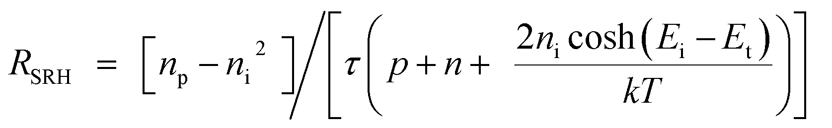 | (5) |
| τ = 1/[σ × Nt × Vth] | (6) |
Here 1014 cm−3 is the Nt of the perovskite layer is the reason for showing the best PCE in the evaluating process. So, by setting up this as defect density of absorber then further evaluating process is done so far.
3.6 Optimization of ETL's features
 | ||
| Fig. 6 The effect of the (a) donor, and (b) defect density variation of ETL. | ||
In this section, the ND of the ETL (TiO2) layer is varied from 9 × 1010 cm−3 to 9 × 1020 cm−3, and also observed the output parameters, i.e. JSC, VOC, FF, and PCE of PSC are to find the optimum performance. At an ND of 9 × 1016 cm−3, the PSC shows the best performance. By setting the ND of ETL as 9 × 1016 cm−3 next evaluation process is conducted. Also from Fig. 6(a), it is identified that in the variation of ND of ETL, there is no significant change of VOC, JSC. Also, the FF and PCE are almost significantly increased to it show the optimum performance. Because a larger ETL's ND value makes carrier extraction and transmission easier at the ETL/perovskite interface. The recombination rate is unaffected because VOC is constant and independent of doping density. This indicates that recombination has remained constant.75 The electric behavior of a layer, which may be changed by adding a dopant, has a big impact on the PV performance of solar cells. ETL and HTL doping increases the performance by increasing the electric field of the interface which enhances the separation mechanism.76 The interface electric field is created by the difference in the Fermi levels of the ETL/absorber and absorber/HTL materials. When the ETL and HTL are doped, the Fermi levels of the materials are shifted and create a higher built-in potential at the interface. This creates a larger electric field at the interface, which helps to drive the charge carriers away from the interface and prevent recombination. The doping of the ETL and HTL increases the concentration of charge carriers in the materials and creates a larger difference in the Fermi levels of the materials, which in turn creates a larger electric field at the interface. The doping of the ETL and HTL can also change the band alignment at the interface. This can further increase the electric field at the interface.
3.7 Optimization of properties of the HTL
 | ||
| Fig. 7 Effect of (a) acceptor density and (b) defect density variation of HTL. | ||
The ETL and HTL doping can be performed in one of two ways. Firstly, it can be done using minority carriers, but the photovoltaic characteristics are substantially reduced. On the other hand, the majority of carriers may achieve this greatly by increasing the PV parameters. The PSCs will perform better if doping density is kept at a moderate level.63 As the NA of HTL increases, the VOC also increases. The greater value of VOC at greater NA can be attributed to an enhancement in the built-in voltages at the HTL/perovskite interface77 which results in increasing electric potential. This improves the PCE of the PSC by reinforcing charge carrier separation with lower recombination.78
Finally, 1013 cm−3 is the Nt of HTL, which was the optimized one for the best PCE and set up for the next evaluation purpose.
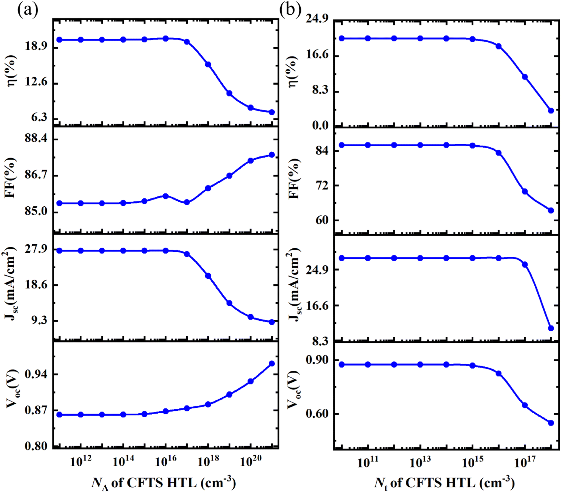
3.8 Optimization of the interface layer's defect density
 | ||
| Fig. 8 Effect of (a) CFTS/CsPbBr3, and (b) CsPbBr3/TiO2 interface defect density variation. | ||
 | (7) |
3.9 Impact of shunt resistance, series resistance, and temperature
 | ||
| Fig. 9 Impact of (a) series resistance, (b) shunt resistance, and (c) temperature variation. | ||
 | (8) |
The ideality factor is denoted by A1, while the thermal voltage is denoted by  . Furthermore, when the temperature rises, the flaws defect increases, resulting in a reduction in VOC. However, when the temperature rises, the FF and PCE values decrease, possibly due to a decrease in shunt resistance.82 Also from Fig. 9(c), it is depicted that the optimum PCE is finding out at 300 K temperature which is room temperature. This optimal temperature was similar to those found in prior studies.86
3.10 Effect of capacitance, Mott–Schottky, generation and recombination rates
In the case of capacitance and the Mott–Schottky effect Fig. 10(a) and (b) show the pattern whenever voltage is changed from −0.5 to 0.8 V in the case of both optimized with HTL and without HTL anointed devices. In both cases, the frequency is considered as 1 MHz. From Fig. 10(a) it is clearly visible that with HTL connected device shows an exponentially increasing capacitance pattern, after 0.4 V it shows drastically increasing capacitance and at the terminating point it shows 200 nF cm−2. Whereas, without HTL connected mode shows almost constant capacitance as depicted in Fig. 10. | ||
| Fig. 10 (a) Capacitance, (b) Mott–Schottky plot, (c) generation rate, (d) recombination rate for PSC. | ||
Fig. 10(c) and (d) show the generation and recombination rate of TiO2 as ETL, and CFTS as HTL-associated CsPbBr3-based solar cell structure. Fig. 10(c) with HTL-connected structure shows the highest generation rate. Whereas in the case of recombination rate according to Fig. 10(d) without HTL connected mode shows the highest recombination rate.
3.11 Output parameters of the simulated final PSC
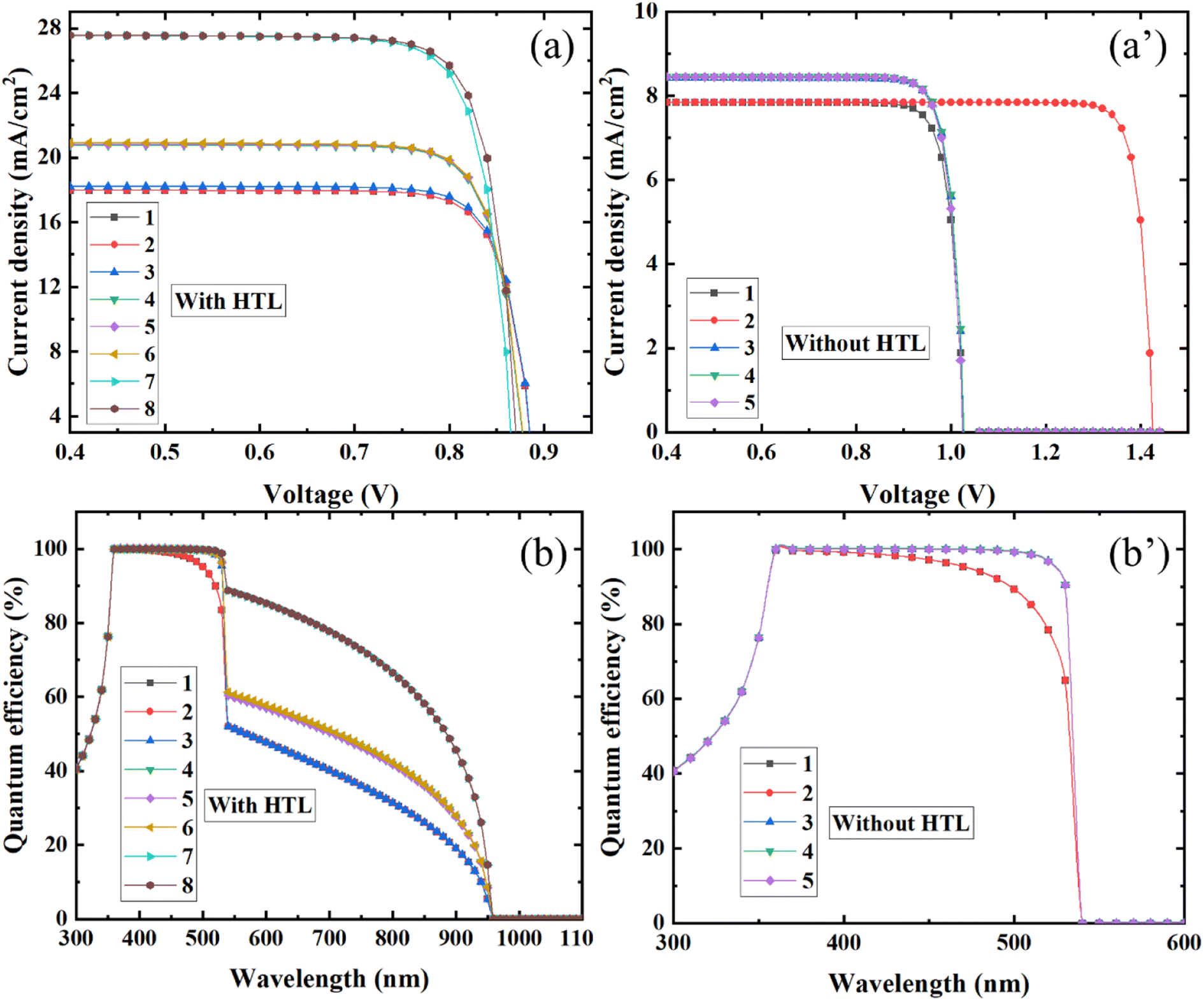 | ||
| Fig. 11 (a, a′) J–V characteristics curve for with and without HTL, and (b, b′) quantum efficiency curve for with and without HTL. | ||
Because the photoelectrons are generated in the layers and the recombination of the electron–hole can become dominant in describing the PV performance of the device. The quantity of defects in perovskite films plays a substantial role in deciding the PSCs output. The J–V curve and VOC in a perovskite film are plotted in Fig. 11(a) and a′, as a function of bulk trap density and so on. The presence of defect states in the perovskite layer is lower than all PV metrics significantly. This is in line with the finding that perovskites' strong crystalline helps to reduce recombination of the charge and so allows for great performance.87
3.12 Assessment of SCAPS-1D results with earlier work
A comparison of optimized solar cell structures is conducted in this section. Here, in Table 4 improved parameters of the PSC's HTL, the absorber layer, and ETL data are given. After many trials and errors, the optimized solar cell structure is found to be ITO/TiO2/CsPbBr3/CFTS/Ni, which shows the best performance. The VOC of 0.875 V, JSC of 27.57 mA cm−2, FF of 85.93%, and PCE of 20.73%, respectively, for the proposed cell.| Parameters | CFTS | CsPbBr3 | TiO2 |
|---|---|---|---|
| Thickness (μm) | 0.25 | 1.8 | 0.03 |
| Eg (eV) | 1.3 | 2.3 | 3.2 |
| χ (eV) | 3.3 | 3.6 | 3.9 |
| εr | 9 | 6.5 | 9 |
| NC (cm−3) | 2.2 × 10¹⁸ | 4.94 × 10¹⁷ | 2 × 10¹⁸ |
| NV (cm−3) | 1.8 × 10¹⁹ | 8.47 × 10¹⁸ | 1.8 × 10¹⁹ |
| μn (cm2 V−1 s−1) | 21.98 | 4500 | 20 |
| μh (cm2 V−1 s−1) | 21.98 | 4500 | 10 |
| NA (cm−3) | 1 × 10¹⁶ | 0 | 0 |
| ND (cm−3) | 0 | 1 × 10¹⁶ | 9 × 10¹⁶ |
| Nt (cm−3) | 1.0 × 10¹³ | 1.0 × 10¹⁴ | 1.0 × 10¹⁵ |
Several CsPbBr3 absorber layer-based devices published during the year 2016–2023 are compared and listed in Table 5. Experimental and theoretical works are categorized as types 1 and 2, respectively. Table 5 shows that different device architectures based on distinct ETL and HTL materials are proposed and investigated but the conversion efficiency remained below 12% due to low JSC values as shown in Table 5. Lower JSC values are attributed to the wide bandgap of CsPbBr3 resulting in low cutoff wavelength and inefficient spectrum utilization. However, the addition of CFTS significantly increased the spectrum utilization which resulted in improved JSC (17.98 mA cm−2) and PCE (13.86%).49 Further optimization reported in this work improved the performance of the CFTS-based device by delivering JSC (27.57 mA cm−2) and PCE (20.73%) as shown in Table 5.
| Typea | Device structure | VOC (V) | JSC (mA cm−2) | FF (%) | PCE (%) | Year | Ref. |
|---|---|---|---|---|---|---|---|
| a 1 - experimental, 2 - theoretical.b This work. | |||||||
| 1 | m-TiO2/CsPbBr3/carbon | 1.24 | 7.4 | 73.0 | 6.70 | 2016 | 33 |
| 1 | m-TiO2/CQD/CsPbBr3 IO/spiro/Ag | 1.06 | 11.34 | 69.0 | 8.29 | 2017 | 88 |
| 1 | FTO/TiO2/CsPbBr3/MoS2 QDs | 1.31 | 6.55 | 79.4 | 6.80 | 2018 | 89 |
| 1 | FTO/c-TiO2/m-TiO2/CsPbBr3/NiOx/C | 1.40 | 6.84 | 76.1 | 7.29 | 2018 | 90 |
| 1 | TiO2/CsPbBr3/CuPc/carbon | 1.26 | 6.62 | 74.0 | 6.21 | 2018 | 91 |
| 1 | m-TiO2/GQDs/CsPbBr3/CISZ-QDs/C | 1.52 | 7.35 | 84.0 | 9.43 | 2018 | 92 |
| 1 | m-TiO2/GQDs/CsPbBr3/C | 1.46 | 8.12 | 82.0 | 9.72 | 2018 | 93 |
| 1 | FTO/GQDs/CsPbBr3/PQDs/carbon | 5.08 | 1.21 | 66.7 | 4.10 | 2018 | 94 |
| 2 | FTO/TiO2/CsPbBr3/NiO/Au | 1.11 | 8.65 | 42.0 | 4.04 | 2019 | 95 |
| 1 | FTO/TiO2/I-CsPbBr3/carbon | 1.29 | 7.07 | 59.0 | 5.38 | 2019 | 96 |
| 1 | FTO/a-Nb2O5/CsPbBr3/CuPc/carbon | 1.45 | 5.64 | 70.0 | 5.74 | 2019 | 97 |
| 1 | FTO/TiO2/CsPbBr3/spiro-MeOTAD/Ag | 1.12 | 7.04 | 68.1 | 5.36 | 2019 | 98 |
| 1 | m-TiO2/CsPbBr3/PTAA/Au | 1.28 | 6.24 | 74.0 | 5.95 | 2020 | 99 |
| 1 | FTO/mp-TiO2/CsPbBr3 | 1.27 | 6.13 | 56.7 | 4.43 | 2020 | 100 |
| 1 | FTO/TiO2/CsPbBr3 + 3% L-lysine/carbon | 1.56 | 7.64 | 81.0 | 9.68 | 2020 | 101 |
| 1 | FTO/c-TiO2/Sn doped CsPbBr3/carbon | 1.36 | 9.27 | 71.0 | 8.95 | 2021 | 102 |
| 2 | FTO/TiO2/CsPbBr3/spiro-MeOTAD | 1.68 | 8.17 | 84.4 | 11.58 | 2020 | 103 |
| 2 | ITO/GO/CsPbBr3/PEDOT:PSS/Au | 1.57 | 8.50 | 77.4 | 10.34 | 2021 | 104 |
| 2 | ITO/TiO2/CsPbBr3/CFTS/Ni | 0.89 | 17.98 | 87.0 | 13.86 | 2023 | 49 |
| 2 | ITO/TiO2/CsPbBr3/CFTS/Ni | 0.87 | 27.57 | 85.9 | 20.73 | 2023 | b |
This concludes that the TiO2 as ETL, CFTS as HTL, and Finally CsPbBr3 as the light-absorbing layer offers the best possible output parameters. This combination of solar cells makes the highly efficient than the other solar cell structures. The light-absorbing layer plays a crucial role in solar cell efficiency. Many other researchers are also working on the CsPbBr3 light absorber layer. But in this work by trial and error choosing appropriate ETL, HTL and their optoelectronic parameters make the solar cell structure more effective and efficient than the other with a PCE of 20.73%.
4 Conclusion
In summary, we have demonstrated a comprehensive simulation approach for optimizing the performance of CsPbBr3-based PSCs. We first optimized the BMC with HTL connected mode and then optimized the CsPbBr3, TiO2, and CFTS layers thickness, charge carrier density, defect density, and interface defect densities as well in both additions of HTL and deduction of the HTL connected conditions. Our optimization process led to the following results:1. The ITO/TiO2/CsPbBr3/CFTS/Ni structure with optimized BMC showed a PCE of 13.86% with HTL-connected condition.
2. We evaluated the impact of absorber thickness concerning absorber defect density and acceptor density on the ITO/TiO2/CsPbBr3/CFTS/Ni structure and achieved a maximum PCE of 14%.
3. The optimized final thickness of the CsPbBr3 absorber, TiO2 ETL, and CFTS HTL were found to be 1.8, 0.03, and 0.25 μm, respectively, in both with and without HTL-connected conditions.
4. We determined the optimized absorber acceptor, defect, and donor densities, as well as the optimized defect density and doping density of the ETL and HTL layers. The final optimized device showed a PCE of 20.73%, with the optimized HTL/absorber and absorber/ETL interface defect densities at 1 × 1010 cm−2. Here, in most cases, with HTL-connected mode shows the best performance.
5. Interfacial defect density remained unchanged during the optimization process and showed the best performance with the initial condition.
Moreover, we investigated the impact of temperature, series and shunt resistance, capacitance, Mott–Schottky, recombination and generation rates, J–V and QE features of the optimized devices both with and without HTL connected conditions. Our study provides valuable insights for designing and constructing high-performance PSCs.
Data availability
The raw/processed data required to reproduce these findings cannot be shared at this time as the data also forms part of an ongoing study.Author contributions
M. K. Hossain: conceptualization, data curation, formal analysis, funding acquisition, investigation, methodology, project administration, resources, software, supervision, validation, visualization, writing – original draft, and writing – review & editing; S. Bhattarai, A. A. Arnab, M. K. A. Mohammed, and R. Pandey: data curation, formal analysis, investigation, software, validation, visualization, and writing – original draft; M. H. Ali, M. F. Rahman, M. R. Islam, D. P. Samajdar, J. Madan, and H. Bencherif, D. K. Dwivedi, and Mongi Amami: data curation, formal analysis, investigation, validation, visualization, and writing – review & editing.Conflicts of interest
The authors declare that they have no known competing financial interests or personal relationships that could have appeared to influence the work reported in this paper.Acknowledgements
The authors have extend their appreciation to the Deanship of Scientific Research at King Khalid University, Saudi Arabia for funding this work through Research Groups Program under grant number R.G.P.2: 200/44. The SCAPS-1D program was kindly provided by Dr M. Burgelman of the University of Gent in Belgium. The authors would like to express their gratitude to him.References
- M. Asif and T. Muneer, Renewable Sustainable Energy Rev., 2007, 11, 1388–1413 CrossRef.
- M. H. K. Rubel, S. K. Mitro, M. K. Hossain, K. M. Hossain, M. M. Rahaman, J. Hossain, B. K. Mondal, A. Akter, M. F. Rahman, I. Ahmed and A. K. M. A. Islam, Mater. Today Commun., 2022, 33, 104302 CrossRef CAS.
- S. Saurabh, M. K. Hossain, S. Singh, S. K. Agnihotri and D. P. Samajdar, RSC Adv., 2023, 13, 9878–9891 RSC.
- M. Shahbaz, A. Siddiqui, M. Siddiqui, Z. Jiao and P. Kautish, Sustain. Energy Technol. Assessments, 2023, 57, 103157 CrossRef.
- M. R. Islam, M. S. Islam, M. Y. Zamil, N. Ferdous, C. Stampfl, J. Park and M. K. Hossain, J. Phys. Chem. Solids, 2023, 176, 111263 CrossRef CAS.
- M. F. Rahman, M. M. Alam Moon, M. K. Hossain, M. H. Ali, M. D. Haque, A. Kuddus, J. Hossain and A. B. Md. Ismail, Heliyon, 2022, 8, e12034 CrossRef CAS PubMed.
- M. E. Islam, M. R. Islam, S. Ahmmed, M. K. Hossain and M. F. Rahman, Phys. Scr., 2023, 98, 065501 CrossRef.
- M. Hasan Ali, A. T. M. Saiful Islam, M. D. Haque, M. Ferdous Rahman, M. Khalid Hossain, N. Sultana and A. Z. M. Touhidul Islam, Mater. Today Commun., 2023, 34, 105387 CrossRef CAS.
- M. K. A. Mohammed, A. K. Al-Mousoi, S. Singh, A. Kumar, M. K. Hossain, S. Q. Salih, P. Sasikumar, R. Pandey, A. A. Yadav and Z. M. Yaseen, Opt. Mater., 2023, 138, 113702 CrossRef.
- S.-C. Yang, T.-Y. Lin, M. Ochoa, H. Lai, R. Kothandaraman, F. Fu, A. N. Tiwari and R. Carron, Nat. Energy, 2022, 8, 40–51 CrossRef.
- N. Shrivastav, S. Kashyap, J. Madan, A. K. Al-Mousoi, M. K. A. Mohammed, M. K. Hossain, R. Pandey and J. Ramanujam, Energy Fuels, 2023, 37, 3083–3090 CrossRef CAS.
- A. K. Al-Mousoi, M. K. A. Mohammed, A. Kumar, R. Pandey, J. Madan, D. Dastan, M. K. Hossain, P. Sakthivel, G. Anandha babu and Z. M. Yaseen, Phys. Chem. Chem. Phys., 2023, 25, 16459–16468 RSC.
- Y. Luo, G. Chen, S. Chen, N. Ahmad, M. Azam, Z. Zheng, Z. Su, M. Cathelinaud, H. Ma, Z. Chen, P. Fan, X. Zhang and G. Liang, Adv. Funct. Mater., 2023 DOI:10.1002/adfm.202213941.
- S. Kashyap, J. Madan, M. K. A. Mohammed, M. K. Hossain, S. Ponnusamy and R. Pandey, Mater. Lett., 2023, 339, 134096 CrossRef CAS.
- S. Heckeroth, (February–March 2010), The Promise of Thin-Film Solar, Mother Earth News, retrieved March 23, 2010, Mother Earth News.
- M. K. Hossain, A. A. Arnab, R. C. Das, K. M. Hossain, M. H. K. Rubel, M. F. Rahman, H. Bencherif, M. E. Emetere, M. K. A. Mohammed and R. Pandey, RSC Adv., 2022, 12, 34850–34873 RSC.
- Y.-H. Kim, H. Cho, J. H. Heo, T.-S. Kim, N. Myoung, C.-L. Lee, S. H. Im and T.-W. Lee, Adv. Mater., 2015, 27, 1248–1254 CrossRef CAS PubMed.
- L. Dou, Y. (Micheal) Yang, J. You, Z. Hong, W.-H. Chang, G. Li and Y. Yang, Nat. Commun., 2014, 5, 5404 CrossRef CAS PubMed.
- M. K. Hossain, M. H. K. Rubel, G. F. I. Toki, I. Alam, M. F. Rahman and H. Bencherif, ACS Omega, 2022, 7, 43210–43230 CrossRef CAS PubMed.
- N. Elumalai, M. Mahmud, D. Wang and A. Uddin, Energies, 2016, 9, 861 CrossRef.
- H. Bencherif, F. Meddour, M. H. Elshorbagy, M. K. Hossain, A. Cuadrado, M. A. Abdi, T. Bendib, S. Kouda and J. Alda, Micro Nanostruct., 2022, 171, 207403 CrossRef CAS.
- H. Bencherif and M. K. Hossain, Sol. Energy, 2022, 248, 137–148 CrossRef CAS.
- A. Kojima, K. Teshima, Y. Shirai and T. Miyasaka, J. Am. Chem. Soc., 2009, 131, 6050–6051 CrossRef CAS PubMed.
- Best Research-Cell Efficiency Chart, by National Renewable Energy Laboratory (NREL), USA, 2021, https://www.nrel.gov/pv/assets/pdfs/cell-pv-eff-emergingpv.pdf Search PubMed.
- N. J. Jeon, H. Na, E. H. Jung, T.-Y. Yang, Y. G. Lee, G. Kim, H.-W. Shin, S. Il Seok, J. Lee and J. Seo, Nat. Energy, 2018, 3, 682–689 CrossRef CAS.
- J. Liang, J. Liu and Z. Jin, Sol. RRL, 2017, 1, 1700086 CrossRef.
- Z. Chen, J. J. Wang, Y. Ren, C. Yu and K. Shum, Appl. Phys. Lett., 2012, 101, 093901 CrossRef.
- S. Z. Y. Hu, F. Bai, X. Liu, Q. Ji, X. Miao and T. Qiu, ACS Energy Lett., 2017, 2, 2219–2227 CrossRef.
- D. Bai, J. Zhang, Z. Jin, H. Bian, K. Wang, H. Wang, L. Liang, Q. Wang and S. F. Liu, ACS Energy Lett., 2018, 3, 970–978 CrossRef CAS.
- C. Liu, W. Li, C. Zhang, Y. Ma, J. Fan and Y. Mai, J. Am. Chem. Soc., 2018, 140, 3825–3828 CrossRef CAS PubMed.
- Y. Wang, T. Zhang, F. Xu, Y. Li and Y. Zhao, Sol. RRL, 2018, 2, 1700180 CrossRef.
- Y. Li, J. Duan, H. Yuan, Y. Zhao, B. He and Q. Tang, Sol. RRL, 2018, 2, 1800164 CrossRef.
- J. Liang, C. Wang, Y. Wang, Z. Xu, Z. Lu, Y. Ma, H. Zhu, Y. Hu, C. Xiao, X. Yi, G. Zhu, H. Lv, L. Ma, T. Chen, Z. Tie, Z. Jin and J. Liu, J. Am. Chem. Soc., 2016, 138, 15829–15832 CrossRef CAS PubMed.
- S. Bhattarai, M. K. Hossain, R. Pandey, J. Madan, D. P. Samajdar, M. F. Rahman, M. Z. Ansari and M. Amami, Energy Fuels, 2023 DOI:10.1021/acs.energyfuels.3c01659.
- A. Kumar, M. K. A. Mohammed, M. U. Khandaker, H. I. Elsaeedy, T. C. A. Kumar, G. B. Ramaiah and M. K. Hossain, J. Mater. Sci. Mater. Electron., 2023, 34, 1343 CrossRef CAS.
- M. K. Hossain, G. F. I. Toki, A. Kuddus, M. H. K. Rubel, M. M. Hossain, H. Bencherif, M. F. Rahman, M. R. Islam and M. Mushtaq, Sci. Rep., 2023, 13, 2521 CrossRef CAS PubMed.
- A. Isha, A. Kowsar, A. Kuddus, M. K. Hossain, M. H. Ali, M. D. Haque and M. F. Rahman, Heliyon, 2023, 9, e15716 CrossRef CAS PubMed.
- N. Shrivastav, S. Kashyap, J. Madan, M. K. A. Mohammed, M. K. Hossain and R. Pandey, Optik, 2023, 281, 170821 CrossRef CAS.
- D. Yang, R. Yang, K. Wang, C. Wu, X. Zhu, J. Feng, X. Ren, G. Fang, S. Priya and S. Liu, Nat. Commun., 2018, 9, 3239 CrossRef PubMed.
- X. Kang, S. Liu, Z. Dai, Y. He, X. Song and Z. Tan, Catalysts, 2019, 9, 191 CrossRef.
- H. Park and W. Choi, J. Phys. Chem. B, 2004, 108, 4086–4093 CrossRef CAS.
- A. B. Wong, S. Brittman, Y. Yu, N. P. Dasgupta and P. Yang, Nano Lett., 2015, 15, 4096–4101 CrossRef CAS PubMed.
- P. Sinsermsuksakul, L. Sun, S. W. Lee, H. H. Park, S. B. Kim, C. Yang and R. G. Gordon, Adv. Energy Mater., 2014, 4, 1400496 CrossRef.
- H. Song, X. Zhan, D. Li, Y. Zhou, B. Yang, K. Zeng, J. Zhong, X. Miao and J. Tang, Sol. Energy Mater. Sol. Cells, 2016, 146, 1–7 CrossRef CAS.
- H. Katagiri, K. Saitoh, T. Washio, H. Shinohara, T. Kurumadani and S. Miyajima, Sol. Energy Mater. Sol. Cells, 2001, 65, 141–148 CrossRef CAS.
- M. K. Hossain, G. F. I. Toki, J. Madan, R. Pandey, H. Bencherif, M. K. A. Mohammed, M. R. Islam, M. H. K. Rubel, M. F. Rahman, S. Bhattarai and D. P. Samajdar, New J. Chem., 2023, 47, 8602–8624 RSC.
- M. K. Hossain, G. F. I. Toki, D. P. Samajdar, M. Mushtaq, M. H. K. Rubel, R. Pandey, J. Madan, M. K. A. Mohammed, M. R. Islam, M. F. Rahman and H. Bencherif, ACS Omega, 2023, 8(25), 22466–22485 CrossRef CAS PubMed.
- P. Kevin, M. A. Malik and P. O'Brien, New J. Chem., 2015, 39, 7046–7053 RSC.
- M. K. Hossain, M. K. A. Mohammed, R. Pandey, A. A. Arnab, M. H. K. Rubel, K. M. Hossain, M. H. Ali, M. F. Rahman, H. Bencherif, J. Madan, M. R. Islam, D. P. Samajdar and S. Bhattarai, Energy Fuels, 2023, 37, 6078–6098 CrossRef CAS.
- T. Dureja, A. Garg, S. Bhalla, D. Bhutani and A. Khanna, Mater. Today: Proc., 2022, 71, 239–242 CAS.
- M. K. Hossain, D. P. Samajdar, R. C. Das, A. A. Arnab, M. F. Rahman, M. H. K. Rubel, M. R. Islam, H. Bencherif, R. Pandey, J. Madan and M. K. A. Mohammed, Energy Fuels, 2023, 37, 3957–3979 CrossRef CAS.
- M. F. Rahman, M. J. A. A. Habib, M. H. Ali, M. H. K. K. Rubel, M. R. Islam, A. B. Md. Ismail and M. K. Hossain, AIP Adv., 2022, 12, 105317 CrossRef CAS.
- D. Dastan, M. K. A. Mohammed, A. K. Al-Mousoi, A. Kumar, S. Q. Salih, P. S. JosephNg, D. S. Ahmed, R. Pandey, Z. M. Yaseen and M. K. Hossain, Sci. Rep., 2023, 13, 9076 CrossRef CAS PubMed.
- M. H. Ali, M. A. Al Mamun, M. D. Haque, M. F. Rahman, M. K. Hossain, A. Z. Md and T. Islam, ACS Omega, 2023, 8, 7017–7029 CrossRef CAS PubMed.
- R. Pandey, S. Bhattarai, K. Sharma, J. Madan, A. K. Al-Mousoi, M. K. A. Mohammed and M. K. Hossain, ACS Appl. Electron. Mater., 2023 DOI:10.1021/acsaelm.2c01574.
- M. F. Rahman, N. Mahmud, I. Alam, M. H. Ali, M. M. A. Moon, A. Kuddus, G. F. I. Toki, M. H. K. Rubel, M. A. Al Asad and M. K. Hossain, AIP Adv., 2023, 13, 045309 CrossRef CAS.
- M. K. Hossain, G. F. Ishraque Toki, D. P. Samajdar, M. H. K. Rubel, M. Mushtaq, M. R. Islam, M. F. Rahman, S. Bhattarai, H. Bencherif, M. K. A. Mohammed, R. Pandey and J. Madan, Energy Fuels, 2023, 37, 7380–7400 CrossRef CAS.
- M. K. A. Mohammed, A. K. Al-Mousoi, A. Kumar, M. M. Sabugaa, R. Seemaladinne, R. Pandey, J. Madan, M. K. Hossain, B. S. Goud and A. A. Al-Kahtani, J. Alloys Compd., 2023, 963, 171246 CrossRef CAS.
- A. Thakur, D. Singh and S. Kaur Gill, Mater. Today: Proc., 2022, 71, 195–201 CAS.
- Y. Raoui, H. Ez-Zahraouy, N. Tahiri, O. El Bounagui, S. Ahmad and S. Kazim, Sol. Energy, 2019, 193, 948–955 CrossRef CAS.
- F. Behrouznejad, S. Shahbazi, N. Taghavinia, H.-P. Wu and E. Wei-Guang Diau, J. Mater. Chem. A, 2016, 4, 13488–13498 RSC.
- N. Singh, A. Agarwal and M. Agarwal, Sol. Energy, 2020, 208, 399–410 CrossRef CAS.
- U. Mandadapu, S. V. Vedanayakam and K. Thyagarajan, Indian J. Sci. Technol., 2017, 10, 1–8 CrossRef.
- L. Lin, L. Jiang, P. Li, B. Fan and Y. Qiu, J. Phys. Chem. Solids, 2019, 124, 205–211 CrossRef CAS.
- M. Kumar, A. Raj, A. Kumar and A. Anshul, Opt. Mater., 2021, 111, 110565 CrossRef CAS.
- A. Tara, V. Bharti, S. Sharma and R. Gupta, Opt. Mater., 2021, 119, 111362 CrossRef CAS.
- S. Bhattarai and T. D. Das, Opt. Mater., 2021, 111, 110661 CrossRef CAS.
- A. Kumar, S. Maurya, S. Patwardhan and K. R. Balasubramaniam, J. Phys. D: Appl. Phys., 2021, 54, 185108 CrossRef CAS.
- J. Adeyemi Owolabi, M. Yusuf Onimisi, J. Amuchi Ukwenya, A. Bulus Bature, U. Raphael Ushiekpan, J. A. Owolabi, M. Y. Onimisi, J. A. Ukwenya, A. B. Bature and U. R. Ushiekpan, Am. J. Phys. Appl., 2020, 8, 8 Search PubMed.
- O. Ahmad, A. Rashid, M. W. Ahmed, M. F. Nasir and I. Qasim, Opt. Mater., 2021, 117, 111105 CrossRef CAS.
- K.-G. Lim, S. Ahn, H. Kim, M.-R. Choi, D. H. Huh and T.-W. Lee, Adv. Mater. Interfaces, 2016, 3, 1500678 CrossRef.
- S. Z. Haider, H. Anwar and M. Wang, Phys. Status Solidi, 2019, 216, 1900102 CrossRef.
- D. Chen, Y. Wang, Z. Lin, J. Huang, X. Chen, D. Pan and F. Huang, Cryst. Growth Des., 2010, 10, 2057–2060 CrossRef CAS.
- Y. Chen, H. Shen and P. P. Altermatt, Sol. Energy Mater. Sol. Cells, 2014, 120, 356–362 CrossRef CAS.
- R. Jeyakumar, A. Bag, R. Nekovei and R. Radhakrishnan, J. Electron. Mater., 2020, 49, 3533–3539 CrossRef CAS.
- P. Roy, N. K. Sinha, S. Tiwari and A. Khare, IOP Conf. Ser.: Mater. Sci. Eng., 2020, 798, 012020 CAS.
- Y. Cao, X. Zhu, H. Chen, X. Zhang, J. Zhouc, Z. Hu and J. Pang, Sol. Energy Mater. Sol. Cells, 2019, 200, 109945 CrossRef CAS.
- A. Mohandes, M. Moradi and H. Nadgaran, Opt. Quantum Electron., 2021, 53, 319 CrossRef CAS.
- F. Anwar, R. Mahbub, S. S. Satter and S. M. Ullah, Int. J. Photoenergy, 2017, 2017, 1–9 CrossRef.
- N. Jensen, R. M. Hausner, R. B. Bergmann, J. H. Werner and U. Rau, Prog. Photovolt.: Res. Appl., 2002, 10, 1–13 CrossRef CAS.
- R. Singh, S. Sandhu and J.-J. Lee, Sol. Energy, 2019, 193, 956–961 CrossRef CAS.
- N. Singh, A. Agarwal and M. Agarwal, Superlattices Microstruct., 2021, 149, 106750 CrossRef CAS.
- Z. Shi, S. Li, Y. Li, H. Ji, X. Li, D. Wu, T. Xu, Y. Chen, Y. Tian, Y. Zhang, C. Shan and G. Du, ACS Nano, 2018, 12, 1462–1472 CrossRef CAS PubMed.
- Z. Ma, Z. Shi, C. Qin, M. Cui, D. Yang, X. Wang, L. Wang, X. Ji, X. Chen, J. Sun, D. Wu, Y. Zhang, X. J. Li, L. Zhang and C. Shan, ACS Nano, 2020, 14, 4475–4486 CrossRef CAS PubMed.
- Y. Li, Z. Shi, L. Lei, F. Zhang, Z. Ma, D. Wu, T. Xu, Y. Tian, Y. Zhang, G. Du, C. Shan and X. Li, Chem. Mater., 2018, 30, 6744–6755 CrossRef CAS.
- M. K. Hossain, G. F. I. Toki, I. Alam, R. Pandey, D. P. Samajdar, M. F. Rahman, M. R. Islam, M. H. K. Rubel, H. Bencherif, J. Madan and M. K. A. Mohammed, New J. Chem., 2023, 47, 4801–4817 RSC.
- M. Liu, M. B. Johnston and H. J. Snaith, Nature, 2013, 501, 395–398 CrossRef CAS PubMed.
- S. Zhou, R. Tang and L. Yin, Adv. Mater., 2017, 29, 1703682 CrossRef PubMed.
- J. Duan, D. Dou, Y. Zhao, Y. Wang, X. Yang, H. Yuan, B. He and Q. Tang, Mater. Today Energy, 2018, 10, 146–152 CrossRef.
- H. Yuan, Y. Zhao, J. Duan, Y. Wang, X. Yang and Q. Tang, J. Mater. Chem. A, 2018, 6, 24324–24329 RSC.
- Z. Liu, B. Sun, X. Liu, J. Han, H. Ye, T. Shi, Z. Tang and G. Liao, Nano-Micro Lett., 2018, 10, 34 CrossRef PubMed.
- J. Duan, Y. Zhao, B. He and Q. Tang, Angew. Chemie, 2018, 130, 3849–3853 CrossRef.
- H. Xu, J. Duan, Y. Zhao, Z. Jiao, B. He and Q. Tang, J. Power Sources, 2018, 399, 76–82 CrossRef CAS.
- J. Duan, Y. Zhao, B. He and Q. Tang, Small, 2018, 14, 1704443 CrossRef PubMed.
- M. Mehrabian, S. Dalir, G. Mahmoudi, B. Miroslaw, M. G. Babashkina, A. V. Dektereva and D. A. Safin, Eur. J. Inorg. Chem., 2019, 2019, 3699–3703 CrossRef CAS.
- J. Liu, L. Zhu, S. Xiang, Y. Wei, M. Xie, H. Liu, W. Li and H. Chen, Sustain. Energy Fuels, 2019, 3, 184–194 RSC.
- F. Zhao, Y. Guo, X. Wang, J. Tao, J. Jiang, Z. Hu and J. Chu, Sol. Energy, 2019, 191, 263–271 CrossRef CAS.
- Z. Zhou, Y. Deng, P. Zhang, D. Kou, W. Zhou, Y. Meng, S. Yuan and S. Wu, Sol. RRL, 2019, 3, 1800354 CrossRef.
- M. Kulbak, D. Cahen and G. Hodes, J. Phys. Chem. Lett., 2015, 6, 2452–2456 CrossRef CAS PubMed.
- E. J. Lee, D.-H. Kim, R. P. H. Chang and D.-K. Hwang, ACS Appl. Energy Mater., 2020, 3, 10376–10383 CrossRef CAS.
- W. Zhang, X. Liu, B. He, J. Zhu, X. Li, K. Shen, H. Chen, Y. Duan and Q. Tang, ACS Appl. Mater. Interfaces, 2020, 12, 36092–36101 CrossRef CAS PubMed.
- M. H. Abib, J. Li, H. Yang, M. Wang, T. Chen, E. Xu and Y. Jiang, RSC Adv., 2021, 11, 3380–3389 RSC.
- S. Ullah, P. Liu, J. Wang, P. Yang, L. Liu, S.-E. Yang, H. Guo, T. Xia and Y. Chen, Sol. Energy, 2020, 209, 79–84 CrossRef CAS.
- M. Mehrabian, E. N. Afshar and S. A. Yousefzadeh, Mater. Res. Express, 2021, 8, 035509 CrossRef CAS.
| This journal is © The Royal Society of Chemistry 2023 |