DOI:
10.1039/D3RA02387G
(Paper)
RSC Adv., 2023,
13, 21852-21860
Annealing effect on the physical properties of TiO2 thin films deposited by spray pyrolysis
Received
11th April 2023
, Accepted 27th June 2023
First published on 19th July 2023
Abstract
Titanium dioxide (TiO2) thin films were deposited on glass substrates at 350 °C using the spray pyrolysis technique. As deposited and annealed thin films were characterized by X-ray diffraction, scanning electron microscopy, UV-VIS spectroscopy, and photodetection. Unlike the as deposited samples which were amorphous, annealed samples show an anatase phase. Films were absorbent in the UV region and the band gap energy decreases from 3.78 eV to 3.4 eV with annealing. The photoresponse of TiO2 photodetectors was recorded under UV (λ1 = 365 nm, λ2 = 254 nm) and visible light illumination by reversible switching (ON/OFF) cycles using DC electrical characterization. Photosensitive properties such as reproducible photosensitivity, responsivity, and detectivity were also studied.
1. Introduction
Photodetectors have attracted a lot of interest in recent decades. Indeed, the conversion of optical signals into electrical ones is a widely required process in many fields, such as optical communication, flame detection, missile guidance and monitoring of the hole in the ozone layer.1–8 Wide band gap semiconductor materials are more important for visible-blind ultra-violet (UV) photodetectors because of their higher optical transmittance in the visible region and superior UV photosensitivity, such as ZnO,9–11 SnO2,12 ZnS,13–15 In2S3,16,17 MoS2,18 and SnS.19 Among these wide bandgap materials TiO2 nanomaterials have great potential in the high-performance photodetector industry thanks to their numerous advantages including excellent chemical stability, abundant reserves, low cost, non-toxicity and their interesting optical and electronic properties.20–25
Furthermore, they are suitable for many applications such as solar cells, photocatalytic activity, and optoelectronic devices. TiO2 can exist as an amorphous structure and also in three crystalline phases: the anatase, the rutile, and the brookite crystal structures with band gap energies of about 3.4 eV, 3 eV and 3.14 eV respectively.26 The uniformity and quality of TiO2 thin films depend on the deposition technique. There are several well-established physical and chemical techniques listed in the literature to deposit TiO2 thin films such as RF sputtering,27 pulsed laser deposition (PLD),28 metal–organic chemical vapor deposition (MOCVD),29 spray pyrolysis30 and sol–gel.31
The aim of this work is to investigate the effect of the annealing on the physical, physiochemical and UV sensing properties of TiO2 thin films deposited by a simple, low cost and eco-friendly spray pyrolysis method. Generally, the UV sensing properties are tested on Si(substrate)/TiO2/Ag metal–semiconductor–metal (MSM) devices, where Ag is used as a contact electrode. In this paper, we use a glass/TiO2/Ag insulator–semiconductor–metal (ISM) device.
2. Experimental techniques
2.1. Preparation of thin films
TiO2 thin films were prepared using the spray pyrolysis technique. Microscope glass slides were used as a substrate for thin films. Prior to the deposition, the glass substrates were cleaned with acetone, ethanol, and distilled water using an ultrasonic bath cleaner. The cleaned substrates were dried for 10 min before use. The precursor solution was prepared by mixing 1 ml titanium(IV) isopropoxide Ti(OC3H7)4, dissolved with 8 ml of isopropanol, 10 ml of acetic acid (CH3COOH), 12 ml of ethanol, and 30 ml of distilled water. Solution was stirred with a magnetic stirrer at 50 °C for one hour. The spraying time was about 10 min at 350 °C and the nitrogen (N2) pressure was 0.5 bar. Annealing was performed for two hours at 500 °C.
2.2. Characterization techniques
Structural properties of the TiO2 films were studied using a Bruker D8 ADVANCE A25 X-ray diffraction system (XRD) equipped with a Cu source (wavelength λ = 1.5418 Å) in the range 2θ = 20–80°. Field Emission Scanning Electron Microscope (FESEM) SCIOS 2 FIB-SEM was used to observe the morphology of the TiO2 films. The FESEM microscope was endowed with an electron dispersive spectrometer (EDS) for chemical analyses. In order to investigate the optical properties (transmittance, gap energy, Urbach energy), the films were characterized by a Shimadzu UV-3101 PC spectrophotometer in the wavelength range of 300–2000 nm. Fig. 1 shows the principle of the photodetection measurements. The sample is subjected to an adjustable polarization and the current intensity through TiO2 thin films is measured using an HP4140B source/pico-ammeter interfaced to a personal computer via a GPIB card. The response versus time is measured by switching On and Off UV (λ1 = 365 nm, λ2 = 254 nm, from an He–Cd laser) and visible light illumination (from a halogen lamp) with 60 s intervals.
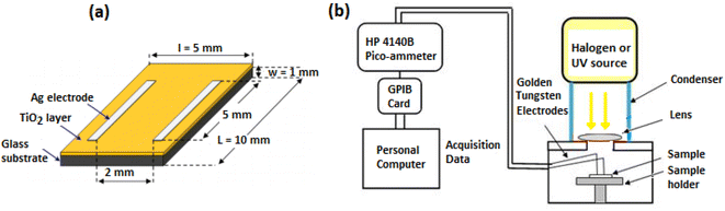 |
| | Fig. 1 (a) Shape of TiO2 sample, (b) photoconductivity experimental set-up. | |
3. Results and discussion
3.1. Structural properties
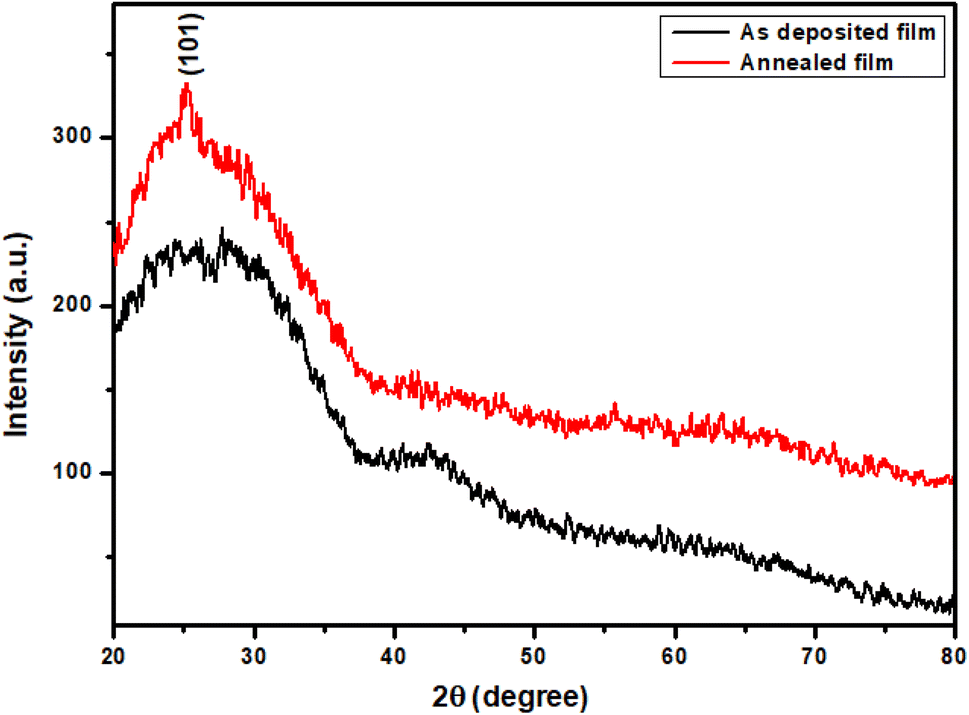
Fig. 2 shows the XRD patterns for TiO2 thin films as deposited at 350 °C and annealed at 500 °C. The diffraction pattern of unannealed TiO2 film does not exhibit clear peaks indicating that the film is amorphous. The presence of a small peak in the X-ray diffraction pattern of annealed film proves that the amorphous phase is partially crystallized. So, the film crystallinity is influenced by annealing.32–34 As seen, the peak situated at 25.30° can be assigned to the (101) plan of an anatase phase of TiO2 according to the JCPDS card no. 83-2243.32,35,36
 |
| | Fig. 2 X-ray diffraction patterns of TiO2 thin films before and after annealing at 500 °C. | |
The calculated value of crystallite size (D) of the films was evaluated using Debye–Scherrer's formula as expressed below:37
| |
 | (1) |
where
K = 0.9,
λ,
β, and
θ are the form factor, the X-ray wavelength, the full width at half maximum (FWHM) and the Bragg angle respectively.
In the same way, the microstrain of the annealed films was calculated by using the following relation:37
| |
 | (2) |
The dislocation density δ, defined as the length of the dislocation lines per unit surface of crystal, was computed using the Williamson–Smallman relation:38
| |
 | (3) |
The calculated values of crystallite size, microstrain and dislocation density of annealed film were evaluated from the (101) diffraction peak and found to be 10 nm, 0.016 and 1012 lines per cm2 respectively.
3.2. Morphological characterization
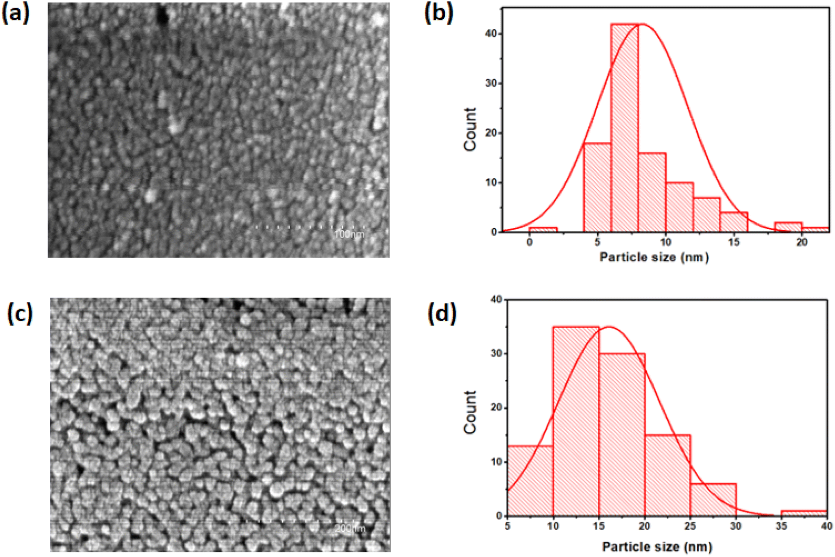
The surface morphology of the TiO2 thin films, investigated by FESEM microscopy, is shown in Fig. 3. On the macroscopic scale, the surface morphology of the films depends on the annealing temperature. As seen in Fig. 3(a), the film surface is rough and granular with small grains. The annealed film presents nearly circular-shaped grains that are distributed over the substrate surface as shown in Fig. 3(c). It is observed that the annealed film became denser with densely packed grains, due to the coalescence phenomenon. The samples are also free of pinholes and cracks. Moreover, the average particle size increases from 8 nm to 16 nm with annealing. These values were deduced from grain size distribution histograms presented in Fig. 3(b and d).
 |
| | Fig. 3 FESEM images and grain size distribution histograms of (a and b) as deposited and (c and d) annealed at 500 °C TiO2 films. | |
The elemental composition for as-deposited and annealed TiO2 films is studied using energy dispersive X-ray spectroscopy (EDX) as shown in Fig. 4. The elemental analysis spectra reveal clearly the presence of the main chemical elements: titanium and oxygen. Also, the spectra show peaks corresponding to Si, Mg, Na, K, Al, and Ca. These elements are coming from the soda–lime glass substrate.39 The obtained atomic percentage (at%) for each film has been listed in the tables in the inset of Fig. 4.
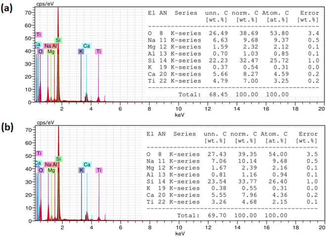 |
| | Fig. 4 EDX spectra and microstructure analysis tables of (a) as deposited and (b) annealed at 500 °C TiO2 films. | |
3.3. Optical properties
3.3.1. Transmittance and absorbance spectra. Transmittance spectra of TiO2 thin films were recorded using UV-visible spectrophotometer. Fig. 5 shows the optical transmittance (T) and absorbance (A) of TiO2 films in the wavelength region of 300–2000 nm. Spectra show the high transmittance and the absence of interference fringes indicating a fairly smooth surface and a relatively good homogeneity of the films. It exhibits a transmission between 65% and 95% in the visible and near infrared regions, which increases with annealing. On the other hand, the absorption spectra show a sharp drop in the UV region for both the films. In addition, the TiO2 films are completely absorbent in the UV region. Therefore, we can deduce that these films may be used as UV detectors and as optical windows in photovoltaic cells.
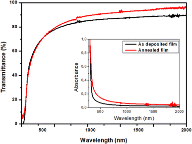 |
| | Fig. 5 Transmittance of TiO2 thin films, in inset, the absorbance spectra. | |
3.3.2. Band gap. The transparency of thin films is mainly influenced by the reflectivity and a combination of absorption coefficient and film thickness. It was determined using the following formula:40where T is the transmittance, R the reflectance and d the film thickness.From the optical transmittance measurements, we can calculate the absorption coefficient (α) of the films. To eliminate the effect of the reflectance, the transmittance (T) is usually related to the absorption coefficient α by using the following formula:41
| |
 | (5) |
The band gap energy (Eg) is deduced from the analysis of the absorption coefficient as a function of the photon energy (hν) in the high absorption region. The optical band gap of the films is estimated by:42
where
A is a constant,
hν is the photon energy,
Eg is the optical band gap energy and the exponent
n is a constant depending on the type of electronic transition. Indeed,
n = 1/2 and 2 correspond to direct allowed and indirect allowed transitions, respectively.
Fig. 6 shows the evolution of (
αdhν)
2 versus hν for TiO
2 films. For this, the nature of the plots suggests a direct interband transition. The band gap energy of the TiO
2 thin films decreases with annealing. For as-deposited films the
Eg was found to be 3.78 eV and a lower value of 3.47 eV was observed for the annealed sample. It is worth mentioning that previous studies have also reported a decrease in the optical band gap of TiO
2 films with the annealing temperature. Such behavior might be the result of the change in film density and the increase in grain size.
43,44 Ziliang Li
et al.45 reported that the usual band gap energy is in the range of 3.0–3.2 eV.
45 In the literature, direct optical band gap values for TiO
2 films vary between 3.20 and 3.90 eV.
46,47 In fact, the bandgap energy increases with the decrease of thickness (from the bulk material to thin film).
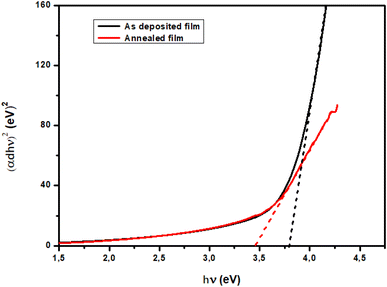 |
| | Fig. 6 (αdhν)2 versus photon energy curve of TiO2 thin films. | |
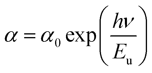
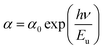
3.3.3. Urbach's energy. Generally, the most important parameter to characterize the disorder in the conduction or valence band or both conduction and valence bands is the Urbach energy. On the other hand, the Urbach energy tailing characterizing the variations of the optical properties, in particular the optical absorption for TiO2 thin film, was calculated by the formula:48–50| |
 | (7) |
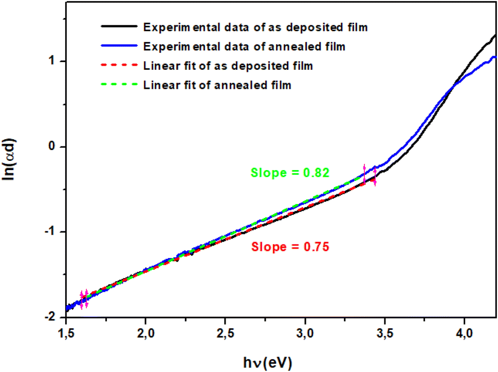
where α is absorption coefficient, α0 is a constant, hν is the photon energy and Eu is the Urbach energy, which is interpreted as the tail of localized states within the band gap. The Eu values were calculated from the inverse of the slope of ln(αd) versus photon energy hν.51 As shown in Fig. 7, Eu values were found to be 1.33 eV and 1.22 eV for the as-deposited and annealed films respectively. The Urbach energy decrease after annealing is due to the crystallinity improvement and the reduced defects and impurity levels. This effect is consistent with FESEM analysis, which shows an increase in grain size resulting from the coalescence phenomenon after the migration of atoms towards their stable equilibrium positions.
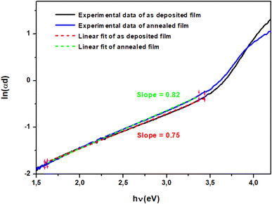 |
| | Fig. 7 ln(αd) versus photon energy curve of the as deposited TiO2 thin film. | |
3.4. Photoconductivity
The study of the TiO2 thin film photo-response has been done by the analysis of the photocurrent in dark and under UV or light illumination of reversible switching (On/Off).
3.4.1. Effect of light. Fig. 8 illustrates the type of the photoresponse for the current intensity through TiO2 films polarized by a voltage of 1 V. Upon UV light illumination at 254 nm, the samples exhibit an obvious photoresponse. In contrast, no photoresponse is observed neither upon white light nor UV 365 nm illumination. The excitation energy is required for electrons to move from the valence band to the conduction band and results in higher photoconductivity, therefore a lower number of electron–hole pairs generation takes place by the absorption of light and recombination is prominent. Also, the curves indicate that the current increases rapidly after illumination and remains constant until the illumination is subsequently turned Off.
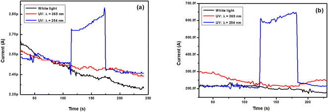 |
| | Fig. 8 Photo-response cycles of TiO2 film (a) as-deposited and (b) annealed at 500 °C, under different illuminations of white light and UV (λ1 = 365 nm, λ2 = 254 nm) with 1 V polarization voltage. | |
On the other hand, Fig. 8(a and b) shows that the dark baseline current of the as-deposited and annealed films are respectively 2.5 pA and 0.2 pA while the steady state current under UV irradiation (λ = 254 nm) for the same films are 2.9 pA and 0.6 pA respectively. Then, the current of the annealed sample is not as good as that of the as-deposited sample. This means that the conductivity of the unannealed film is higher than that of the other sample. In fact, the change in the conductivity σ is determined according to the following equation:
where,
q is the electron charge (
q = 1.6 × 10
−19 C),
μ is the electron mobility and
N is the free electron density which is related to the concentration of oxygen vacancies.
52–54 Liu
et al.55 have shown that there is a dynamic process of adsorption and desorption of oxygen atoms in the film when annealed in air. When the number of oxygen atoms adsorbed in the film is more than the number of oxygen atoms removed, the oxygen vacancies in the film decrease, resulting in a decrease in the density
N. Conversely, the
N increases. In the case of TiO
2, during annealing, the number of oxygen atoms in the air entering the film increases, resulting in a decrease in the concentration of oxygen vacancies. The conductivity decreases as consequence.
3.4.2. Effect of reproducibility. By switching ON the UV source, the measured current obtained for successive square pulses, with the same time length are shown in Fig. 9. After four cycles, no apparent deactivation of the photoconductivity was observed. Therefore, thin films exhibit excellent stability for UV light driven photoresponse.
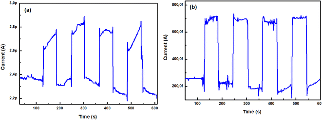 |
| | Fig. 9 Reproducibility for TiO2 layers, (a) as-deposited and (b) annealed at 500 °C, under UV light illumination (λ = 254 nm) switched ON and OFF alternately for 1 V polarization. | |
3.4.3. Effect of polarization voltage. Fig. 10(a and b) depicts the characteristics of photocurrent versus time for different polarizations (1 to 5 V). TiO2 film curves show the alternating current change in dark and under UV light (245 nm). We note that the photocurrent increases with increasing polarization. Fig. 10(c and d) indicates that the photocurrent follows a linear evolution as a function of the bias voltage.| | |
As deposited film: Iph (pA) = 0.27 V + 0.29
| (9) |
| | |
Annealed film: Iph (pA) = 0.19 V + 0.47
| (10) |
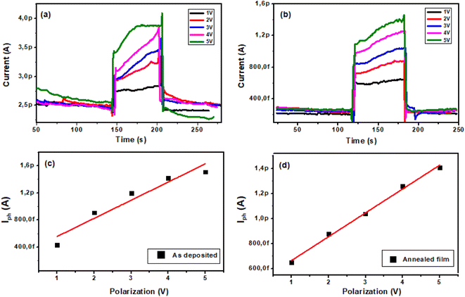 |
| | Fig. 10 Evolution of photocurrent vs. time under UV illumination at polarizations ranging from 1 V to 5 V of TiO2 films: (a) as-deposited film and (b) annealed film. Evolution of photocurrent vs. polarization: (c) as-deposited and (d) annealed film. | |
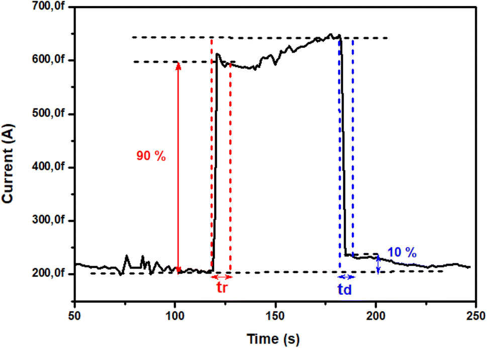
The photoresponse characteristics including the rise time (tr) and decay time (td) measured under 245 nm UV light are shown in Fig. 11, which are the crucial factors to demonstrate device performances. The tr (from 10% to 90% of the top value) is the time of the photogenerated carriers that have to be accumulated to offset the depletion region before achieving a saturation state of device response. Oppositely, the td (from 90% to 10% of the top value) is the time of the recovery of depleting effect and accelerated carrier recombination when converting from UV on to off.56
 |
| | Fig. 11 Rise and decay times of TiO2 under 0.15 mW cm−2 UV light illumination (λ = 254 nm) for 1 V bias. | |
Besides, the photocurrent intensity (Iph) is defined by the following relation:
| | |
Iph = Ilight − Idark
| (11) |
where,
Iph is the photocurrent difference between currents under the light and dark.
Photosensitivity (S) measures the current change of the photodetector upon illumination. It is calculated using the following equation:57
| |
 | (12) |
The photodetector photoresponsivity (R) is the amount of photocurrent generated when the films are illuminated by a light source and it is given by:58
| |
 | (13) |
where,
A = 0.1 cm
2 is the illumination area and
P = 0.15 mW cm
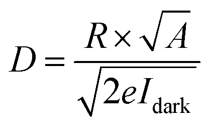
−2 is the light intensity. Detectivity (
D) represents the ability of a photodetector to detect weak optical signals, which can be calculated according to the following equation:
58,59| |
 | (14) |
where,
R is the responsivity and
e the charge of electron.
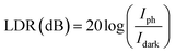
The linear dynamic range (LDR) describes the light intensity range in which the current response of a photodetector is linearly proportional to light intensity, which can be expressed by the following equation:45
| |
 | (15) |
All the analyses were calculated to describe photosensitive properties of TiO2 samples and they are regrouped in Table 1.
Table 1 UV light (λ = 254 nm) photosensitive properties of TiO2 films
| |
TiO2 (as deposited) |
TiO2 (annealed) |
| 1 V |
5 V |
1 V |
5 V |
| Idark (pA) |
2.46 |
2.55 |
0.21 |
0.27 |
| Ilight (pA) |
2.89 |
4.06 |
0.65 |
1.41 |
| Iph(pA) |
0.43 |
1.51 |
0.44 |
1.14 |
| tr (s) |
25.04 |
29.31 |
24.54 |
34.54 |
| td (s) |
5.17 |
4.54 |
2.01 |
2.99 |
| Sensitivity |
0.17 |
0.59 |
2.13 |
4.26 |
| Responsivity (10−8 A W−1) |
2.86 |
10 |
4.32 |
9.4 |
| Detectivity (107 jones) |
1.01 |
3.50 |
5.30 |
10.15 |
| LDR (dB) |
−15.39 |
−4.58 |
6.56 |
12.58 |
The analysis of these curves yields dark current (Id), rise time (tr), decay time (td), sensitivity (S), responsivity (R) and detectivity (D) of the samples which are regrouped in Table 1. We note an increase of all these parameters by raising the polarization. On the other hand, it is noted that annealing improves the photosensitive properties of TiO2 layers, that is, in the case of 1 V polarization, the sensitivity increases 13 times and the detectivity 5 times, while the response speed is not affected by annealing. We note also that the increase of polarization from 1 V to 5 V improves most often photosensitive properties. In fact, this behavior is due to the rise of electron mobility with electric field increase. Yang et al.60 reported that TiO2 thin films polarized at 5 V show under ultraviolet illumination (λ = 365 nm), a rise time tr = 1.13 s, a decay time td = 0.75 s and a sensitivity of 104. In our case, tr and td are in the order of 35 s and 5 s, respectively. In other studies, Chen et al.61 reported a sensitivity of 9 for the NiO/ZnO/Al2O3 structure. Similarly, Wang et al.62 found a value of 10 for the Cu2ZnSnS4/TiO2/Al2O3 structure. These values are comparable to those of our work.
4. Conclusion
In this study, titanium oxide thin films were deposited on glass substrates at 350 °C by the spray pyrolysis technique and then annealed in air at 500 °C. The annealing treatment has remarkably influenced the structural, morphological, optical, and photosensitive properties. XRD analysis reveals that as-deposited films are amorphous while with annealing the amorphous phase is partially crystallized into the anatase one with preserving their (101) preferential orientation. The SEM images show that the layer surfaces are homogeneous, well covered and the grain size rises with annealing. UV-VIS spectra reveal that band gap energy decreases from 3.78 eV to 3.47 eV with annealing. Hence, the photoconductivity study of TiO2 shows that these layers are sensitive to UV light at λ2 = 254 nm. Therefore, these results encourage the use of TiO2 thin films as UV detectors, optical windows in photovoltaic cells and photodiodes in various optoelectronic applications.
Data availability
The datasets generated during and/or analyzed during the current study are available from corresponding author on reasonable request.
Conflicts of interest
There are no conflicts to declare.
Acknowledgements
The authors declare that no funds, grants or other support were received during the preparation of this manuscript. We thank Prof. V. Muñoz-Sanjose and Prof. M.C. Martinez-Tomas from the University of Valencia for providing the use of technical equipment.
References
- D. Zhang, C. Liu, B. Yin, R. Xu, J. Zhou, X. Zhang and S. Ruan, Nanoscale, 2017, 9, 9095–9103 RSC.
- C. C. Ling, T. C. Guo, W. B. Lu, X. F. Li, L. Zhu, M. Ma and Q. Z. Xue, J. Mater. Chem. C, 2018, 6, 2319–2328 RSC.
- S. Sharma, R. Khosla, D. Deva, H. Shrimali and S. K. Sharma, Sens. Actuators, Ac, 2017, 261, 94–102 CrossRef CAS.
- T. Ji, Q. Liu, R. Zou, Y. Zhang, L. Wang, L. Sang, M. Liao and J. Hu, J. Mater. Chem. C, 2017, 5, 12848–12856 RSC.
- L. Zheng, K. Hu, F. Teng and X. Fang, Small, 2017, 13, 1602448 CrossRef.
- P. Deb and J. C. Dhar, Fast, IEEE Photonics Technol. Lett., 2019, 31, 571–574 CAS.
- M. Zhang, T. Kamale, H. Zhang and L. Li, Ultraviolet, Optoelectron. Lett., 2019, 15, 81–84 CrossRef.
- M. H. Zarifi, B. Wiltshire, N. Mahdi, P. Kar, K. Shankar and M. Daneshmand, Nanoscale, 2018, 10, 4882–4889 RSC.
- Y. Zhang, W. Xu, X. Xu, W. Yang, S. Li, J. Chen and X. Fang, Nanoscale Horiz., 2019, 4, 452–456 RSC.
- D. Chen, L. Wei, L. Meng, D. Wang, Y. Chen, Y. Tian, S. Yan, L. Mei and J. Jiao, J. Alloys Compd., 2018, 751, 56–61 CrossRef CAS.
- Y. Wang, J. Cheng, M. Shahid, Y. Xing, Y. Hu, T. Li, M. Zhang, H. Nishijima and W. Pan, Nanotechnology, 2019, 31, 015601 CrossRef PubMed.
- X. Wang, J. Li, X. Gao, Y. Shen and A. Xie, Appl. Surf. Sci., 2019, 463, 357–362 CrossRef CAS.
- W. Zhao, L. He, X. Feng, H. Xiao, C. Luan and J. Ma, Ceram. Int., 2018, 44, 21114–21119 CrossRef CAS.
- S. M. Kumbhar, S. K. Shaikh and K. Y. Rajpure, J. Electron. Mater., 2019, 49, 499–509 CrossRef.
- G. Rawat, D. Somvanshi, H. Kumar, Y. Kumar, C. Kumar and S. Jit, IEEE Trans. Nanotechnol., 2016, 15, 193–200 CAS.
- B. Bouricha, R. Souissi, N. Bouguila, D. Jlidi and A. Labidi, Mater. Res. Express, 2019, 6, 116456 CrossRef.
- M. Toumi, N. Bouguila, R. Souissi, B. Tiss, M. Kraini and S. Alaya, Optik, 2020, 217, 164896 CrossRef CAS.
- Y. H. Zhou, H. N. An, C. Gao, Z. Q. Zheng and B. Wang, Mater. Lett., 2019, 237, 298–302 CrossRef CAS.
- M. S. Mahdi, K. Ibrahim, N. M. Ahmed, A. Hmood, F. I. Mustafa, S. A. Azzez and M. Bououdina, J. Alloys Compd., 2018, 735, 2256–2262 CrossRef CAS.
- J. Chen, J. Xu, S. Shi, R. Cao, D. Liu, Y. Bu, P. Yang, J. Xu, X. Zhang and L. Li, ACS Appl. Mater. Interfaces, 2020, 12, 23145–23154 CrossRef CAS PubMed.
- Y. Gao, J. Xu, S. Shi, H. Dong, Y. Cheng, C. Wei, X. Zhang, S. Yin and L. Li, ACS Appl. Mater. Interfaces, 2018, 10, 11269–11279 CrossRef CAS.
- T. Ji, Y. Cao, X. Peng, Y. Zhang, L. Sun, L. Wang, R. Zou, Y. Sivalingam, W. Han and J. Hu, Appl. Surf. Sci., 2018, 449, 358–362 CrossRef CAS.
- R. Cao, J. Xu, S. Shi, J. Chen, D. Liu, Y. Bu, X. Zhang, S. Yin and L. Li, J. Mater. Chem. C, 2020, 8, 9646–9654 RSC.
- I. Camps, M. Borlaf, M. T. Colomer, R. Moreno, L. Duta, C. Nita, A. Perez del Pino, C. Logofatu, R. Serna and E. György, RSC Adv., 2017, 7, 37643–37653 RSC.
- J. Bai and B. Zhou, Chem. Rev., 2014, 114(19), 10131–10176 CrossRef CAS PubMed.
- T. Tsai, S. Chang, T. Hsueh, H. Hsueh, W. Weng, C. Hsu and B. Dai, Nanoscale Res. Lett., 2011, 6, 1 Search PubMed.
- A. M. Selman and Z. Hassan, Sens. Actuators, A, 2015, 221, 15 CrossRef CAS.
- S. N. Mazhir, G. H. Mohamed, A. A. Abdullah and M. D. Radhi, Int. J. Adv. Res., 2015, 3, 1060 CAS.
- F. Alema, B. Hertog, O. Ledyaev, D. Volovik, R. Miller, A. Osinsky, S. Bakhshi and W. V. Schoenfeld, Sens. Actuators, A, 2016, 249, 263 CrossRef CAS.
- P. S. Shinde, P. S. Patil, P. N. Bhosale, A. Brüger, G. Nauer, M. Neumann-Spallart and C. H. Bhosale, Appl. Catal., B, 2009, 89, 288 CrossRef CAS.
- Y. Xie, H. Huang, W. Yang and Z. Wu, J. Appl. Phys., 2011, 109, 023114 CrossRef.
- M. O. Abou-Helal and W. T. Seeber, Appl. Surf. Sci., 2002, 195, 53–62 CrossRef CAS.
- T. S. Senthil, N. Muthukumarasamy, S. Agilan, M. Thambidurai and R. Balasundaraprabhu, J. Mater. Sci. Eng. B, 2010, 174, 102–104 CrossRef CAS.
- Y. U. Ahn, E. J. Kim, H. T. Kim and S. H. Hanh, Mater. Lett., 2003, 57, 4660–4666 CrossRef CAS.
- F. Hanini, A. Bouabellou, Y. Bouachiba, F. Kermiche, A. Taabouche, M. Hemissi and D. Lakhdari, IOSR J. Eng., 2013, 21–28 Search PubMed.
- R. Kumar, N. Sharma and N. Arora, Adv. Appl. Sci. Res., 2016, 7, 142–147 CAS.
- B. Tiss, M. Erouel, N. Bouguila, M. Kraini and K. Khirouni, J. Alloys Compd., 2018, 771, 60–66 CrossRef.
- G. K. Williamson and R. E. Smallman, Philos. Mag., 1956, 1, 34 CrossRef CAS.
- M. S. Eluyemi, M. A. Eleruja, A. V. Adedeji, B. Olofinjana, O. Fasakin, O. O. Akinwunmi, O. O. Ilori, A. T. Famojuro, S. A. Ayinde and E. O. B. Ajayi, Graphene, 2016, 5, 143–154 CrossRef CAS.
- R. Caballero and C. Guillén, Thin Solid Films, 2003, 431, 200 CrossRef.
- E. Jose and M. C. S. Kumar, SPIE Nanoscience Engineering, 2016, 9929, 992917 Search PubMed.
- N. Pentyala, R. K. Guduru, E. M. Shnerpunas and P. S. Mohanty, Appl. Surf. Sci., 2011, 257, 6850–6857 CrossRef CAS.
- C. V. R. Vasanth Kumar and A. Mansingh, J. Appl. Phys., 1989, 65, 1270 CrossRef.
- F. Hanini, A. Bouabellou, Y. Bouachiba, F. Kermiche, A. Taabouche, M. Hemissi and D. Lakhdari, IOSR J. Eng., 2013, 3, 21–28 Search PubMed.
- Z. Li, Z. Li, C. Zuo and X. Fang, Adv. Mater., 2022, 34(28), 2109083 CrossRef CAS.
- V. N. Kruchinin, T. V. Perevalov, V. V. Atuchin, V. A. Gritsenko, A. I. Komonov, I. V. Korolkov, L. D. Pokrovsky, C. W. Shih and A. Chin, J. Electron. Mater., 2017, 46, 6089 CrossRef CAS.
- F. Atay and D. Durmaz, Structural, J. Electron. Mater., 2020, 49, 5542–5551 CrossRef CAS.
- S. Ilican, Y. Caglar and M. Caglar, J. Optoelectron. Adv. Mater., 2008, 10, 2578–2583 CAS.
- C. O. Ayieko, R. J. Musembi, S. M. Waita, B. O. Aduda and P. K. Jain, Int. J. Energy Eng., 2012, 2, 67–72 CrossRef.
- S. M. AL-Shomar, Mater. Res. Express, 2021, 8, 026402 CrossRef CAS.
- S. Ilican, Y. Caglar, M. Caglar, M. Kundakci and A. Ates, Int. J. Hydrogen Energy, 2009, 12, 5201–5207 CrossRef.
- K. Y. Chen, S. P. Chang and C. h. Lin, RSC Adv., 2019, 9, 87–90, 10.1039/c8ra08803a.
- W. Huang, J. Shi, Y. Liu, F. Meng and Z. Liu, J. Alloys Compd., 2020, 843, 155151 CrossRef CAS.
- J. Yu, J. Zhou, J. Bian, L. Zhang, Y. Liu, J. Shi, F. Meng, J. Liu and Z. Liu, Jpn. J. Appl. Phys., 2017, 56, 08MB09 CrossRef.
- H. Liu, Y. Gong, H. Diao, X. Jia, L. Zhao, W. Wang, W. Wang, J. Zong, J. Mater. Sci.: Mater. Electron., 2023, 34, 840 CrossRef.
- D. Zhang, C. Liu, B. Yin, R. Xu, J. Zhou, X. Zhang and S. Ruan, Nanoscale, 2017, 26, 365505 Search PubMed.
- M. S. Mahdi, K. Ibrahim, A. Hmood, N. M. Ahmed, S. A. Azzez and F. I. Mustafa, RSC Adv., 2016, 6, 114980–114988 RSC.
- K. S. Gour, O. P. Singh, B. Bhattacharyya, R. Parmar, S. Husale, T. D. Senguttuvan and V. N. Singh, J. Alloys Compd., 2017, 694, 119–123 CrossRef CAS.
- B. Hemanth Kumar and M. C. Santhosh Kumar, Sens. Actuators, A, 2019, 299, 111643 CrossRef.
- D. Yang, Y. Ren, F. Du, P. Hu, Y. Jiao, F. Teng and H. Fan, J. Alloys Compd., 2021, 867, 159053 CrossRef CAS.
- Z. Chen, B. Li, X. Mo, S. Li, J. Wen, H. Lei, Z. Zhu, G. Yang, P. Gui, F. Yao and G. Fang, Appl. Phys. Lett., 2017, 110, 123504 CrossRef.
- Z. Wang, N. Brodusch, R. Gauvin and G. P. Demopoulos, J. Mater. Chem. A, 2018, 6, 11507–11520 RSC.
|
| This journal is © The Royal Society of Chemistry 2023 |
Click here to see how this site uses Cookies. View our privacy policy here. 
 Open Access Article
 This Open Access Article is licensed under a Creative Commons Attribution-Non Commercial 3.0 Unported Licence
 b,
M. Toumia,
M. Madania,
L. El Mira,
N. Bouguila
b,
M. Toumia,
M. Madania,
L. El Mira,
N. Bouguila