
 Open Access Article
 This Open Access Article is licensed under a Creative Commons Attribution-Non Commercial 3.0 Unported Licence
Simultaneously enhancing the photovoltaic parameters of ternary organic solar cells by incorporating a fused ring electron acceptor†
Min Zhang‡
a,
Xiaoyuan Chen‡b,
Lei Wangb,
Xiong Dengb and
Songting Tan *b
*b
aModern Industry School of Advanced Ceramics, Hunan Provincial Key Laboratory of Fine Ceramics and Powder Materials, Hunan University of Humanities, Science and Technology, Lou'di, Hunan 417000, China
bKey Laboratory of Environmentally Friendly Chemistry and Applications of Ministry of Education, College of Chemistry, Xiangtan University, Xiangtan 411105, China. E-mail: tanst2008@163.com
First published on 9th June 2023
Abstract
The ternary strategy has been recognized as an effective method to improve the photovoltaic performance of organic solar cells (OSCs). In ternary OSCs, the complementary or broadened absorption spectrum, optimized morphology, and enhanced photovoltaic performance could be obtained by selecting a third rational component for the host system. In this work, a fused ring electron acceptor named BTMe-C8-2F, which possesses a high-lying lowest unoccupied molecular orbital (LUMO) energy level and a complementary absorption spectrum to PM6:Y6, was introduced to a PM6:Y6 binary system. The ternary blend film PM6:Y6:BTMe-C8-2F showed high and more balanced charge mobilities, and low charge recombination. Therefore, the OSC based on the PM6:Y6:BTMe-C8-2F (1![[thin space (1/6-em)]](https://www.rsc.org/images/entities/char_2009.gif) :1.2:0.3, w/w/w) blend film achieved the highest power conversion efficiency (PCE) of 17.68%, with an open-circuit voltage (VOC) of 0.87 V, a short-circuit current (JSC) of 27.32 mA cm−2, and a fill factor (FF) of 74.05%, which are much higher than the binary devices of PM6:Y6 (PCE = 15.86%) and PM6:BTMe-C8-2F (PCE = 11.98%). This work provides more insight into the role of introducing a fused ring electron acceptor with a high-lying LUMO energy level and complementary spectrum for simultaneously enhancing the VOC and JSC to promote the performance of ternary OSCs.
:1.2:0.3, w/w/w) blend film achieved the highest power conversion efficiency (PCE) of 17.68%, with an open-circuit voltage (VOC) of 0.87 V, a short-circuit current (JSC) of 27.32 mA cm−2, and a fill factor (FF) of 74.05%, which are much higher than the binary devices of PM6:Y6 (PCE = 15.86%) and PM6:BTMe-C8-2F (PCE = 11.98%). This work provides more insight into the role of introducing a fused ring electron acceptor with a high-lying LUMO energy level and complementary spectrum for simultaneously enhancing the VOC and JSC to promote the performance of ternary OSCs.
1. Introduction
As an urgently needed supplementary energy in the near future and the foundation of future energy structures, organic solar cells (OSCs) have huge potential due to the advantages of environmental protection, solution processing and low cost.1–5 With the innovation of donor and acceptor materials, the power conversion efficiency (PCE) has been increasing constantly.6–10 In 2019, Zou et al. synthesized a novel molecule acceptor Y6, which boosted the PCE to 15.7% when being matched with the classic polymer donor PM6.11 Since then, a boost of the efficiency has been triggered by the continuous innovation of the molecular structure and the improvement of device manufacturing.12–15The ternary strategy, which has been proven to have multiple virtues such as reduced energy loss and optimized morphology, is considered to be an efficient way to promote photovoltaic performance. In the strategy, a third component with a complementary absorption spectrum and suitable energy level, is demanded and incorporated into the binary systems to broaden the spectrum and improve the active layer morphology,16–22 further enhancing the JSC23,24 and VOC.25 Generally, the third component is a donor26 or an acceptor27,28 to fabricate OSCs with the active layers as D/A1/A2 or D1/D2/A, respectively.29 However, an extra donor incorporated into the binary system often leads to absorption overlap.30 Then ternary OSCs with D/A1/A2 active layer emerges gradually when an acceptor with appropriate energy level and spectrum introduced into a binary system.31–37 However, in some cases, a smaller bandgap acceptor with a low-lying LUMO energy level is incorporated into the binary system to better cover the NIR region and improve JSC, which often leads to a reduced VOC. For instance, a fused ring electron acceptor named IEICF-DMOT incorporated as the guest acceptor into the PBDB-T:IEICO-4F binary system, the obtained ternary device with the ratio of 1:1:0.1 showed a high PCE of 14.00% with a distinctly improved JSC of 23.31 mA cm−2 but a reduced VOC of 0.86 V.38 Hence, selecting an acceptor with complementary absorption and high-lying LUMO level as the third component introduces to the binary system will hopefully enhance the JSC and keep the VOC at a high level.
During cyclization in the small molecule acceptor synthesis, the isomerization usually generates by the multiple cyclization reaction sites on the benzene ring, which will cause the uncertainty of the molecular structure.39–41 In our previous work,42 a small molecule acceptor named BTMe-C8-2F with benzo[b]benzo[4,5]thieno[2,3-d]thiophene (BTBT) unit as the core was synthesized. The incorporation of the methyl group in the core worked as the positioning group prevented the isomerization and increased the cyclization yield effectively. Moreover, the material possesses a high-lying LUMO level of −4.03 eV and a suitable absorption in the range of 550–750 nm, which has great potential in constructing ternary OSCs based on the binary PM6:Y6. In this contribution, a series of ternary devices were fabricated by introducing BTMe-C8-2F into the host PM6:Y6 system, which was expected to bring a higher JSC and VOC simultaneously. When PM6:Y6:BTMe-C8-2F blended film with the ratio of 1:1.2:0.3 (w/w/w), the device showed an excellent PCE of 17.68% with a significantly enhanced a JSC of 27.32 mA cm−2, a VOC of 0.87 V and a FF of 74.03%.
2. Results and discussion
The chemical structures of PM6, Y6, and BTMe-C8-2F are shown in Fig. 1(a). The UV-vis absorption spectra of them in films are shown in Fig. 1(b), and the relevant parameters are shown in Table 1. In the host system, PM6 shows strong absorption in the range of 500–700 nm with an absorption peak at 617 nm, and Y6 shows strong absorption in the range of 700–900 nm with an absorption peak at 834 nm. As the third component BTMe-C8-2F, which exhibits the absorption in the range of 550–750 nm with peaks at 622 and 681 nm, achieving complementary absorption to the host materials. In addition, from the absorption spectra with different contents of BTMe-C8-2F shown in Fig. 1(c), the binary blend film of PM6:BTMe-C8-2F shows strong absorption in the range of 450–750 nm with two distinct peaks at 625 and 674 nm, which are derived from the absorption of PM6 and BTMe-C8-2F, respectively. In the binary blend film of PM6:Y6, a broad spectrum ranging from 450 to 900 nm is observed. The absorption peak in the long wavelength (812 nm) is attributed to Y6, while the absorption peak in the short wavelength (625 nm) assign to PM6. For the ternary films, the absorption spectra range from 450 nm to 900 nm. And with the increase of BTMe-C8-2F, the spectra exhibit an enhanced absorption in the medium wavelength range, which indicates that the introduction of an appropriate amount of BTMe-C8-2F could effectively complement the absorption spectrum.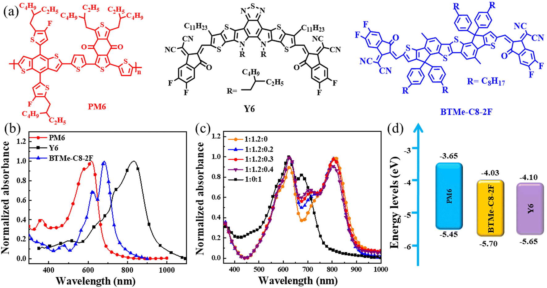 | ||
| Fig. 1 (a) Molecular structures; (b) absorption spectra of PM6, Y6 and BTMe-C8-2F in films; (c) absorption spectra of binary and ternary blends with different weight ratios of BTMe-C8-2F; (d) energy levels of PM6, BTMe-C8-2F and Y6. | ||
The LUMO and HOMO of PM6,43 BTMe-C8-2F and Y6 (ref. 11) are shown in Fig. 1(d). And more detailed parameters were listed in Table 1. The third component BTMe-C8-2F shows the intermediate LUMO level and the lowest HOMO level in three materials. Generally, the energy level offset between the HOMO and LUMO determines the dissociation of photoexcited charges at the D–A interface. However, since the not very discreet energy levels44 and the existence of energetic disorder,45 it is difficult to predict the energetic landscape. To understand the charge transfer between the donor and acceptors, photoluminescence (PL) spectra were performed. As shown in Fig. S1,† when excited at 560 nm, the pure film of PM6 shows a relatively strong emission peak, but when PM6 mixed with Y6 (binary) or with Y6 and BTMe-C8-2F (ternary), the emission peak intensity significantly reduced, suggesting that the donor has an effective charge transfer to the acceptors. To further explore the charge transfer between BTMe-C8-2F and Y6, PL spectra measured with an excitation wavelength of 623 nm. As shown in Fig. S2,† BTMe-C8-2F pure film shows a fluorescence peak at 724 nm. When BTMe-C8-2F and Y6 mixed at 0.7:0.3 (w/w), the fluorescence peak red-shifts to 829 nm with a quenching efficiency of about 68%. And the fluorescence peak almost disappeared and the quenching efficiency reached 93% when the content of Y6 increased to 70%. These results show that the excited electrons are efficiently transferred from BTMe-C8-2F to Y6.
The compatibility of the guest acceptor and host materials was investigated by contact angle test. And the contact angles (CA) of PM6, Y6, and BTMe-C8-2F pure films with water and ethylene glycol (EG) were measured and shown in Fig. 2 and Table S1.† When water drops upon the pure films, the contact angles of PM6, Y6 and BTMe-C8-2F pure films are 100.50°, 91.25° and 92.50°, respectively. When EG drops upon the pure films, the contact angles of PM6, Y6 and BTMe-C8-2F pure films are 70.25°, 65.50° and 66.00°, respectively. Therefore, according to Owens–Wendt–Kaelble's model,46 the surface energy of PM6, Y6 and BTMe-C8-2F pure films are calculated as 30.82, 26.89 and 27.37 mN m−1, respectively. Then the Flory–Huggins interaction parameters (χ), which can reflect the miscibility of the two materials, could be further obtained. Generally, the smaller the χ value, the better miscibility of the materials.47,48 As a result, the χ values for PM6:Y6 and PM6:BTMe-C8-2F are assessed as 0.134 K and 0.102 K, respectively. And the corresponding parameter of Y6:BTMe-C8-2F is only 0.002 K. The relatively small χ of the blend film suggests that Y6 and BTMe-C8-2F could form a well-mixed acceptor phase in the ternary blend films, which would facilitated the separation and transportation of the charges.49
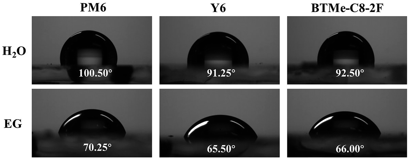 | ||
| Fig. 2 The images of water and EG drops upon PM6, Y6 and BTMe-C8-2F pure films. | ||
To further explore the compatibility of BTMe-C8-2F and Y6, the differential scanning calorimetry (DSC) was used to perform for the melting and crystallization behaviors (Fig. S3†). For the neat Y6, a phase transformation peak at 257.5 °C (ΔH = 4.05 J g−1) and a melting peak at 299.8 °C (ΔH = 23.7 J g−1) are observed in the heating process. And a weak crystallization peak at 204.9 °C (ΔH = 3.5 J g−1) also appeared in the cooling process. In terms of BTMe-C8-2F, there are no significant signals of melting and crystallization points, which suggest the low crystallinity. While for Y6:BTMe-C8-2F blend, the melting point move to the lower temperature of 296.0 °C (ΔH = 17.2 J g−1), which indicates the excellent miscibility and a well-mixed acceptor phase of BTMe-C8-2F and Y6 is formed.50
The morphologies of the ternary blend film with the ratio of 1:1.2:0.2, 1:1.2:0.3, 1:1.2:0.4 were analyzed by atomic force microscopy (AFM).51–53 As shown in Fig. 3, all ternary blend films display smooth surfaces with the root mean square (RMS) roughness values are 1.44 nm for 1:1.2:0.2, 1.31 nm for 1:1.2:0.3, and 1.25 nm for 1:1.2:0.4. The small RMS roughness values (<2 nm) of them suggest the excellent compatibility among the donor and acceptors, which conform to the result of the contact angle test. While in the image of the ternary blend film with the ratio of 1:1.2:0.3, a clear and well-proportioned bicontinuous nanophase separation could be observed, which indicates an efficient charge transport could occur.
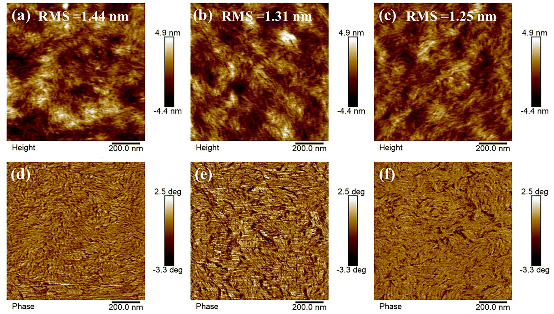 | ||
| Fig. 3 AFM height and phase images of (a and d) 1:1.2:0.2, (b and e) 1:1.2:0.3, and (c and f) 1:1.2:0.4 for PM6:Y6:BTMe-C8-2F blend films. | ||
Grazing incidence wide-angle X-ray scattering (GIWAXS) was used to explore the molecular orientation and packing of the blend films.54 The 2D diagrams and the profiles and the more detailed data of 1:1.2:0.2, 1:1.2:0.3 and 1:1.2:0.4 are displayed in Fig. 4 and Table S2,† respectively. Referring to the result of the binary PM6:Y6 (ref. 11) blend film, since to the π–π stacking of Y6 and the lamellar stacking of PM6 and Y6, a face-on orientation with (010) peak at 1.76 Å−1 (d = 3.57 Å) and a (100) peak at 0.297 Å−1 (d = 21.09 Å) is formed in the out of plane (OOP) and in-plane (IP) direction, respectively. And the other binary film of PM6:BTMe-C8-2F42 also preferred to form a face-on orientation with a (010) peak at 1.79 Å−1 (d = 3.5 Å) and a (100) peak at 0.32 Å−1 (d = 19.6 Å) in the OOP and IP direction, respectively. As for the ternary blend films, strong (010) peaks in the OOP direction at 1.80, 1.76, and 1.78 Å−1 can be seen in the film of 1:1.2:0.2, 1:1.2:0.3 and 1:1.2:0.4, respectively, with the π–π stacking distances are 3.50, 3.57 and 3.53 Å. At the same time, the distinct (100) peaks in the IP direction at 0.305, 0.295 and 0.295 Å−1, also can be observed with the packing distances are 20.6, 21.3 and 21.3 Å, respectively. These results indicate that all ternary blend films tend to form the molecular orientation of face-on, which is conducive to the transport of charge carriers. In addition, the crystalline coherent length (CCL) of 1:1.2:0.2 is 25.45 Å for the (010) peak and 74.83 Å for the (100) peak. And the corresponding values of 1:1.2:0.4 is 24.62 Å for the (010) peak and 72.69 Å for the (100) peak. It is notable that the blend film of 1:1.2:0.3 exhibit the largest CCL with a value of 25.93 Å for the (010) peak and 78.24 Å for the (100) peak, possessing the stronger and more orderly molecular packing and orientation. This result could contribute to a superior JSC, FF and PCE in the corresponding devices.
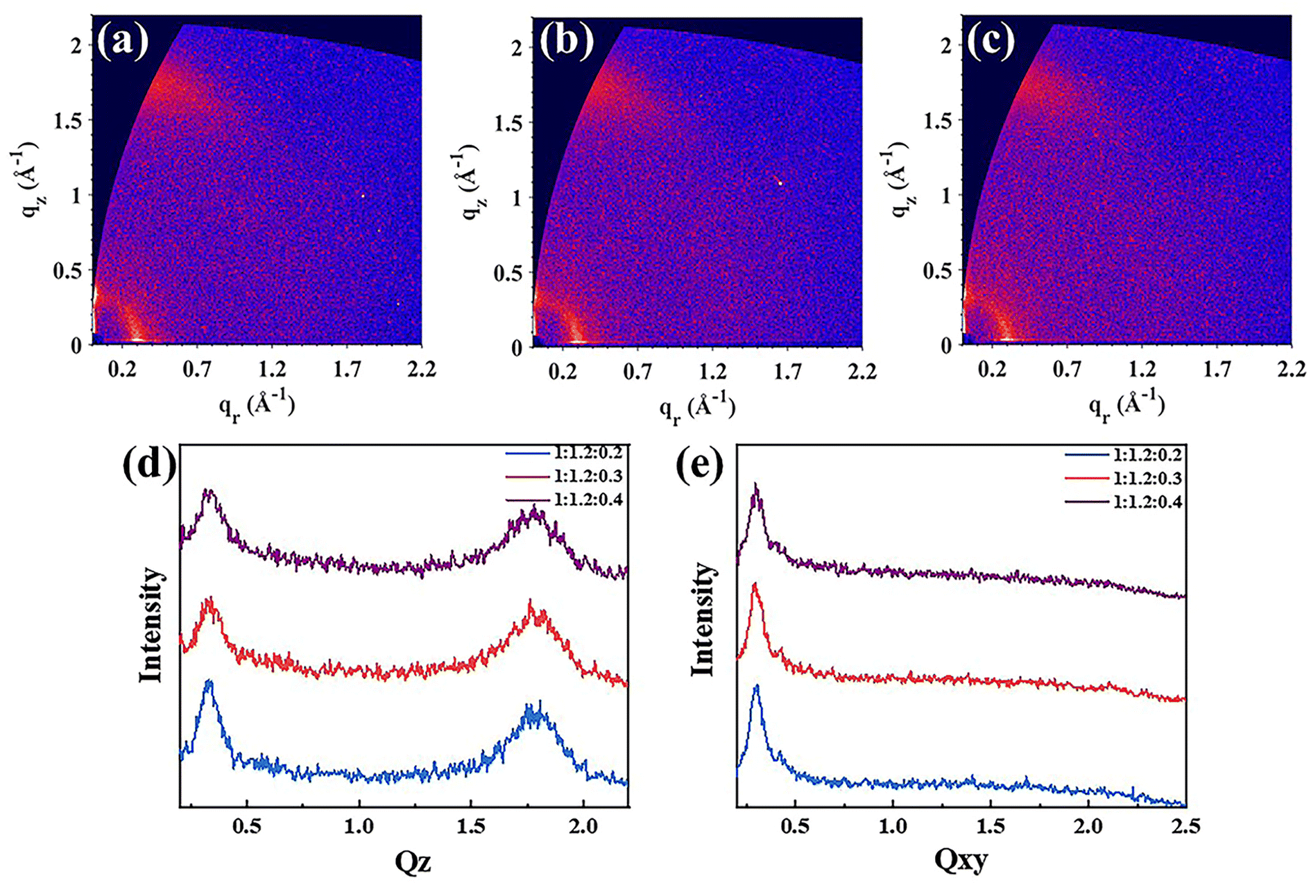 | ||
| Fig. 4 2D GIWAXS images of (a) 1:1.2:0.2, (b) 1:1.2:0.3, (c) 1:1.2:0.4 blend films; (d) the OOP profiles and (e) the IP profiles of the thin films. | ||
To explore the effect of BTMe-C8-2F on the photovoltaic performances of devices, a series of devices were manufactured using the conventional structure of ITO/PEDOT:PSS/active layer/PFN-Br/Ag with an active area of 0.038 cm−2. The J–V curves for the optimized devices are shown in Fig. 5(a), and the detailed performances are shown in Table 2. According to the optimal conditions of the inverted binary device,42 the conventional binary devices based on PM6:BTMe-C8-2F (1:1, w/w) were also manufactured. However, a relatively inferior PCE of 11.98% was obtained with a preferable FF of 71.93% but a slightly lower VOC (0.96 V) and JSC (17.34 mA cm−2) than that of the inverted binary device.42 For the binary PM6:Y6 (1:1.2, w/w) based device, a maximum PCE of 15.86% (JSC = 26.07 mA cm−2, VOC = 0.84 V, FF = 72.76%) was achieved with the postprocessing of the addition of 0.5% (v/v) 1-CN and thermal annealing (TA) treatment at 100 °C for 10 minutes. Under the same condition, the ternary OSCs were prepared with PM6:Y6 kept at 1:1.2 (w/w). By introducing different ratios of BTMe-C8-2F into the active layer, the ternary devices show different photovoltaic performances. With the content of BTMe-C8-2F gradually increase in the ternary system, the VOC enhanced accordingly from 0.84 V to 0.88 V, which illustrates that the guest acceptor with higher LUMO will increase the VOC of the ternary device. The tunable VOC of the devices also suggests that the two acceptors tended to form a homogenous mixed-phase with a gradually elevated LUMO energy level dependent on the BTMe-C8-2F content. At the same time, the JSC also improved from 26.07 mA cm−2 to 27.32 mA cm−2 with the ratio of 1:1.2:0 increasing to 1:1.2:0.3, which can ascribe to the enhancement absorption in medium wavelength by adding BTMe-C8-2F to the system. And the parameter FF, which greatly affected by the morphology and molecular accumulation, exhibits the optimal value of 74.05% in 1:1.2:0.3 based blend film. Owing to the outstanding VOC, JSC and FF, the ternary devices with the ratio of 1:1.2:0.3 displays an optimum PCE of 17.68%, with a VOC of 0.87 V, a JSC of 27.32 mA cm−2, and FF of 74.05%. In addition, the integrated photocurrent from the EQE spectra (Fig. 5(c)) matches well the JSCs measured from the J–V curves. All ternary devices present high response in the wavelength of 300–900 nm. And the incorporation of BTMe-C8-2F obviously increased the EQE spectra from the wavelength range from 450–850 nm in comparison with the binary PM6:Y6, which should do favor to the enhancement the JSC in the ternary devices.
 | ||
| Fig. 5 (a) J–V curves of the devices; (b) histogram of the efficiency with different content of BTMe-C8-2F; (c) EQE spectra of the devices; (d) dependence of VOC on the Plight for devices; (e) dependence of JSC on the Plight for devices; (f) histogram of charge mobility with different content of BTMe-C8-2F. | ||
| PM6:Y6:BTMe-C8-2F |
VOC (V) | JSC (mA cm−2) | FF (%) | PCE (PCEavga) (%) | Jcalc. (mA cm−2) |
|---|---|---|---|---|---|
| a The PCEavg was calculated from 10 devices. The active area of devices is 0.038 cm−2. | |||||
| 1:1.2:0 |
0.84 | 26.07 (25.86 ± 0.67) | 72.76 (72.45 ± 0.40) | 15.86 (15.70 ± 0.20) | 25.56 |
| 1:1.2:0.2 |
0.86 | 26.96 ((26.90 ± 0.38) | 73.53 (73.14 ± 0.54) | 17.00 (16.57 ± 0.36) | 26.07 |
| 1:1.2:0.3 |
0.87 | 27.32 (27.10 ± 0.33) | 74.05 (73.87 ± 0.65) | 17.68 (17.43 ± 0.34) | 26.51 |
| 1:1.2:0.4 |
0.88 | 27.00 (26.90 ± 0.14) | 73.76 (73.45 ± 0.48) | 17.48 (17.33 ± 0.20) | 26.21 |
| 1:0:1 |
0.96 | 17.34 (17.08 ± 0.24) | 71.93 (71.82 ± 0.31) | 11.98 (11.73 ± 0.25) | 17.07 |
To better understand the differences in photovoltaic performance, we evaluate the dependence of VOC, JSC on light intensity (Plight),55–57 respectively, with the curves displayed in Fig. 5(d) and (e). The relationship between VOC and light intensity is described as VOC ∝ ln(P). And the slopes of the fitting lines based on the films with the ratios of 1:1.2:0, 1:1.2:0.2, 1:1.2:0.3, 1:1.2:0.4, 1:0:1 is 1.24, 1.22, 1.12, 1.14 and 1.50KT/q, respectively. Therefore, the slightest slope of 1:1.2:0.3 based blend film shows the lowest monomolecular recombination. Synchronously, the dependence of JSC and light intensity is described as JSC ∝ Plightα (Fig. 5(e)), where the exponential factor α represents the extent of the bimolecular recombination. When the α value is closer to 1, weaker bimolecular recombination is manifested.58,59 Since the α values of the devices of 1:1.2:0, 1:1.2:0.2, 1:1.2:0.3, 1:1.2:0.4, 1:0:1 is 0.990, 0.992, 0.997, 0.993 and 0.969, respectively, the bimolecular recombination in 1:2:0.3 based film is more effectively suppressed, which is beneficial to obtain the higher JSC and FF.
To further understand the effect of the incorporated BTMe-C8-2F on the charge transport properties, the charge transport ability of blend films was characterized by space-charge-limited current (SCLC) method with the J0.5–V curves of hole-only and electron-only devices are shown in Fig. S5.† The more detailed data and the corresponding diagrammatic drawing are provided in Table S3† and Fig. 5(f). In the binary system of PM6:Y6, the hole mobility (μh) and electron mobility (μe) are 6.52 × 10⁻⁴ cm2 V−1 s−1 and 5.52 × 10⁻⁴ cm2 V−1 s−1, respectively, along with the μh/μe ratio of 1.18. For the ternary system, when the weight ratio is 1:1.2:0.2, the μh and μe increased to 7.07 × 10⁻⁴ cm2 V−1 s−1 and 6.27 × 10⁻⁴ cm2 V−1 s−1, respectively, with the μh/μe ratio decreased to 1.13. And when the ratio increased to 1:1.2:0.3, the μh and μe sequentially raised to 9.62 × 10⁻⁴ cm2 V−1 s−1 and 9.20 × 10⁻⁴ cm2 V−1 s−1, respectively, with the μh/μe ratio continue to decrease to 1.04. And the μh and μe turn to inferior in the blend film of 1:1.2:0.4. Therefore, the electron and hole transport channels can be finely optimized. The blend film of 1:1.2:0.3, which exhibits the most appropriate phase separation, possesses the most elevated and more balanced charge mobilities, which is beneficial to obtain higher JSC and FF.60
3. Conclusion
In conclusion, a fused ring electron acceptor BTMe-C8-2F was incorporated into the PM6:Y6 (1:1.2, w/w) binary host system to fabricate ternary OSCs. The complementary light absorption and relatively high-lying LUMO energy level of BTMe-C8-2F are beneficial to enhancing the JSC and VOC of ternary OSCs. Moreover, the blend film with the ratio of 1:1.2:0.3 possesses weaker bimolecular recombination, better morphology, more appropriate molecular stacking and higher charge mobilities. Thus, compared with the binary OSCs based on PM6:Y6 (PCE = 15.86%, VOC = 0.84 V, JSC = 26.07 mA cm−2, and FF = 72.76%), the ternary OSCs based on 1:1.2:0.3 exhibits the highest PCE of 17.68% with synchronously improved JSC of 27.32 mA cm−2, VOC of 0.87 V and FF of 74.05%. The results demonstrate that ternary OSCs can simultaneously enhance the JSC, VOC and FF values by introducing BTMe-C8-2F. This work provides a new perspective on incorporating a fused ring electron acceptor to tune the absorption spectrum and the molecular packing for constructing high-performance ternary OSCs.
Conflicts of interest
The authors declare no conflict of interest.Acknowledgements
The work was funded by the National Natural Science Foundation of China (21875204). The authors thanks Dr Heng Liu and Prof. Xinfei Lu (Department of physics, Chinese University of Hong Kong) for GIWAXS measurements.References
- Q. Yue, W. Liu and X. Zhu, J. Am. Chem. Soc., 2020, 142, 11613–11628 CrossRef CAS PubMed.
- P. Cheng, G. Li, X. Zhan and Y. Yang, Nat. Photonics, 2018, 12, 131–142 CrossRef CAS.
- L.-W. Feng, J. Chen, S. Mukherjee, V. K. Sangwan, W. Huang, Y. Chen, D. Zheng, J. W. Strzalka, G. Wang and M. C. Hersam, ACS Energy Lett., 2020, 5, 1780–1787 CrossRef CAS.
- G. Yu, J. Gao, J. C. Hummelen, F. Wudl and A. J. Heeger, Science, 1995, 270, 1789–1791 CrossRef CAS.
- N. S. Sariciftci, L. Smilowitz, A. J. Heeger and F. Wudl, Science, 1992, 258, 1474–1476 CrossRef CAS PubMed.
- Y. Liu, Z. Zhang, S. Feng, M. Li, L. Wu, R. Hou, X. Xu, X. Chen and Z. Bo, J. Am. Chem. Soc., 2017, 139, 3356–3359 CrossRef CAS PubMed.
- W. Zhao, D. Qian, S. Zhang, S. Li, O. Inganäs, F. Gao and J. Hou, Adv. Mater., 2016, 28, 4734–4739 CrossRef CAS PubMed.
- W. Zhao, S. Li, H. Yao, S. Zhang, Y. Zhang, B. Yang and J. Hou, J. Am. Chem. Soc., 2017, 139, 7148–7151 CrossRef CAS PubMed.
- S. Dey, Small, 2019, 15, 1900134 CrossRef PubMed.
- W. Peng, G. Zhang, L. Shao, C. Ma, B. Zhang, W. Chi, Q. Peng and W. Zhu, J. Mater. Chem. A, 2018, 6, 24267–24276 RSC.
- J. Yuan, Y. Zhang, L. Zhou, G. Zhang, H.-L. Yip, T.-K. Lau, X. Lu, C. Zhu, H. Peng, P. A. Johnson, M. Leclerc, Y. Cao, J. Ulanski, Y. Li and Y. Zou, Joule, 2019, 3, 1140–1151 CrossRef CAS.
- L. Zhu, M. Zhang, J. Xu, C. Li, J. Yan, G. Zhou, W. Zhong, T. Hao, J. Song and X. Xue, Nat. Mater., 2022, 21, 656–663 CrossRef CAS PubMed.
- X. Xu, L. Yu, H. Meng, L. Dai, H. Yan, R. Li and Q. Peng, Adv. Funct. Mater., 2022, 32, 2108797 CrossRef CAS.
- C. Li, J. Zhou, J. Song, J. Xu, H. Zhang, X. Zhang, J. Guo, L. Zhu, D. Wei and G. Han, Nat. Energy, 2021, 6, 605–613 CrossRef CAS.
- K. Chong, X. Xu, H. Meng, J. Xue, L. Yu, W. Ma and Q. Peng, Adv. Mater., 2022, 34, 2109516 CrossRef CAS PubMed.
- L. Zhan, S. Li, Y. Li, R. Sun, J. Min, Z. Bi, W. Ma, Z. Chen, G. Zhou and H. Zhu, Joule, 2022, 6, 662–675 CrossRef CAS.
- Y. Zhu, A. Gadisa, Z. Peng, M. Ghasemi, L. Ye, Z. Xu, S. Zhao and H. Ade, Adv. Energy Mater., 2019, 9, 1900376 CrossRef.
- T. Yan, W. Song, J. Huang, R. Peng, L. Huang and Z. Ge, Adv. Mater., 2019, 31, 1902210 CrossRef PubMed.
- Q. An, J. Wang, W. Gao, X. Ma, Z. Hu, J. Gao, C. Xu, M. Hao, X. Zhang and C. Yang, Sci. Bull., 2020, 65, 538–545 CrossRef CAS PubMed.
- N. Gasparini, A. Salleo, I. McCulloch and D. Baran, Nat. Rev. Mater., 2019, 4, 229–242 CrossRef.
- R. Yu, H. Yao, Y. Cui, L. Hong, C. He and J. Hou, Adv. Mater., 2019, 31, 1902302 CrossRef PubMed.
- Q. Zhao, Z. Xiao, J. Qu, L. Liu, H. Richter, W. Chen, L. Han, M. Wang, J. Zheng, Z. Xie, L. Ding and F. He, ACS Energy Lett., 2019, 4, 1106–1114 CrossRef CAS.
- X. Ma, Y. Mi, F. Zhang, Q. An, M. Zhang, Z. Hu, X. Liu, J. Zhang and W. Tang, Adv. Energy Mater., 2018, 8, 1702854 CrossRef.
- D. Su, M.-A. Pan, Z. Liu, T.-K. Lau, X. Li, F. Shen, S. Huo, X. Lu, A. Xu and H. Yan, Chem. Mater., 2019, 31, 8908–8917 CrossRef CAS.
- P. Bi, S. Zhang, Z. Chen, Y. Xu, Y. Cui, T. Zhang, J. Ren, J. Qin, L. Hong and X. Hao, Joule, 2021, 5, 2408–2419 CrossRef CAS.
- P. Bi, J. Wang, Y. Cui, J. Zhang, T. Zhang, Z. Chen, J. Qiao, J. Dai, S. Zhang, X. Hao, Z. Wei and J. Hou, Adv. Mater., 2023, 35, 2210865 CrossRef CAS PubMed.
- H.-R. Bai, Q. An, M. Jiang, H. S. Ryu, J. Yang, X.-J. Zhou, H.-F. Zhi, C. Yang, X. Li, H. Y. Woo and J.-L. Wang, Adv. Funct. Mater., 2022, 32, 2200807 CrossRef CAS.
- M. Jiang, H.-F. Zhi, B. Zhang, C. Yang, A. Mahmood, M. Zhang, H. Y. Woo, F. Zhang, J.-L. Wang and Q. An, ACS Energy Lett., 2023, 8, 1058–1067 CrossRef CAS.
- Y. D. Nutifafa, Y. Lili and R. Federico, Nano Energy, 2022, 94, 106915 CrossRef.
- J. Ge, Q. Wei, R. Peng, E. Zhou, T. Yan, W. Song, W. Zhang, X. Zhang, S. Jiang and Z. Ge, ACS Appl. Mater. Interfaces, 2019, 11, 44528–44535 CrossRef CAS PubMed.
- X. Wang, Q. Sun, J. Gao, X. Ma, J. H. Son, S. Y. Jeong, Z. Hu, L. Niu, H. Y. Woo and J. Zhang, Sol. RRL, 2021, 5, 2100007 CrossRef CAS.
- Y. Yin, L. Zhan, M. Liu, C. Yang, F. Guo, Y. Liu, S. Gao, L. Zhao, H. Chen and Y. Zhang, Nano Energy, 2021, 90, 106538 CrossRef CAS.
- L. Xiao, X. Wu, G. Ren, M. A. Kolaczkowski, G. Huang, W. Tan, L. Ma, Y. Liu, X. Peng and Y. Min, Adv. Funct. Mater., 2021, 31, 2105304 CrossRef CAS.
- J. Song, C. Li, L. Zhu, J. Guo, J. Xu, X. Zhang, K. Weng, K. Zhang, J. Min, X. Hao, Y. Zhang, F. Liu and Y. Sun, Adv. Mater., 2019, 31, 1905645 CrossRef CAS PubMed.
- M. Zhang, Z. Xiao, W. Gao, Q. Liu, K. Jin, W. Wang, Y. Mi, Q. An, X. Ma and X. Liu, Adv. Energy Mater., 2018, 8, 1801968 CrossRef.
- X. Du, Y. Yuan, L. Zhou, H. Lin, C. Zheng, J. Luo, Z. Chen, S. Tao and L. S. Liao, Adv. Funct. Mater., 2020, 30, 1909837 CrossRef CAS.
- X. Duan, W. Song, J. Qiao, X. Li, Y. Cai, H. Wu, J. Zhang, X. Hao, Z. Tang, Z. Ge, F. Huang and Y. Sun, Energy Environ. Sci., 2022, 15, 1563–1572 RSC.
- Y. Chang, X. Zhang, Y. Tang, M. Gupta, D. Su, J. Liang, D. Yan, K. Li, X. Guo, W. Ma, H. Yan and C. Zhan, Nano Energy, 2019, 64, 103934 CrossRef CAS.
- W. Hu, X. Du, W. Zhuang, W. Su, J. Cao, A. M. Pourrahimi, N. Li, X. Shen, M. Zhang and D. Yu, ACS Appl. Energy Mater., 2020, 3, 5734–5744 CrossRef CAS.
- T. Li, Y. Wu, J. Zhou, M. Li, J. Wu, Q. Hu, B. Jia, X. Pan, M. Zhang and Z. Tang, J. Am. Chem. Soc., 2020, 142, 20124–20133 CrossRef CAS PubMed.
- Z. Zhou, J. Duan, L. Ye, G. Wang, B. Zhao, S. Tan, P. Shen, H. S. Ryu, H. Y. Woo and Y. Sun, J. Mater. Chem. A, 2020, 8, 9684–9692 RSC.
- X. Deng, M. Zi, R. Hao, Y. Qi, P. Yue, P. Shen, B. Zhao and S. Tan, J. Mater. Chem. C, 2021, 9, 13357–13365 RSC.
- M. Zhang, X. Guo, W. Ma, H. Ade and J. Hou, Adv. Mater., 2015, 27, 4655–4660 CrossRef CAS PubMed.
- J. Bertrandie, J. Han, C. S. P. De Castro, E. Yengel, J. Gorenflot, T. Anthopoulos, F. Laquai, A. Sharma and D. Baran, Adv. Mater., 2022, 34, 2202575 CrossRef CAS PubMed.
- S.-U.-Z. Khan, J. Bertrandie, M. Gui, A. Sharma, W. Alsufyani, J. F. Gorenflot, F. Laquai, D. Baran and B. P. Rand, Joule, 2022, 6, 2821–2834 CrossRef CAS.
- A. Lan, Y. Lv, J. Zhu, H. Lu, H. Do, Z.-K. Chen, J. Zhou, H. Wang, F. Chen and E. Zhou, ACS Energy Lett., 2022, 7, 2845–2855 CrossRef CAS.
- D. K. Owens and R. Wendt, J. Appl. Polym. Sci., 1969, 13, 1741–1747 CrossRef CAS.
- J. Comyn, Int. J. Adhes. Adhes., 1992, 12, 145–149 CrossRef CAS.
- X. Xu, C. Sun, J. Jing, T. Niu, X. Wu, K. Zhang, F. Huang, Q. Xu, J. Yuan, X. Lu, Y. Zhou and Y. Zou, ACS Appl. Mater. Interfaces, 2022, 14, 36582–36591 CrossRef CAS PubMed.
- Y. Cai, Y. Li, R. Wang, H. Wu, Z. Chen, J. Zhang, Z. Ma, X. Hao, Y. Zhao and C. Zhang, Adv. Mater., 2021, 33, 2101733 CrossRef CAS PubMed.
- F. Zhao, C. Wang and X. Zhan, Adv. Energy Mater., 2018, 8, 1703147 CrossRef.
- K. H. Hendriks, G. H. Heintges, V. S. Gevaerts, M. M. Wienk and R. A. Janssen, Angew. Chem., 2013, 125, 8499–8502 CrossRef.
- G. Fang, J. Liu, Y. Fu, B. Meng, B. Zhang, Z. Xie and L. Wang, Org. Electron., 2012, 13, 2733–2740 CrossRef CAS.
- P. Müller-Buschbaum, Adv. Mater., 2014, 26, 7692–7709 CrossRef PubMed.
- P. Schilinsky, C. Waldauf and C. J. Brabec, Appl. Phys. Lett., 2002, 81, 3885–3887 CrossRef CAS.
- L. J. A. Koster, V. D. Mihailetchi, R. Ramaker and P. W. Blom, Appl. Phys. Lett., 2005, 86, 123509 CrossRef.
- N. K. Elumalai and A. Uddin, Energy Environ. Sci., 2016, 9, 391–410 RSC.
- C. He, Y. Pan, Y. Ouyang, Q. Shen, Y. Gao, K. Yan, J. Fang, Y. Chen, C.-Q. Ma, J. Min, C. Zhang, L. Zuo and H. Chen, Energy Environ. Sci., 2022, 15, 2537–2544 RSC.
- M. Jiang, H. Bai, H. Zhi, L. Yan, H. Y. Woo, L. Tong, J. Wang, F. Zhang and Q. An, Energy Environ. Sci., 2021, 14, 3945–3953 RSC.
- Q. An, J. Wang, X. Ma, J. Gao, Z. Hu, B. Liu, H. Sun, X. Guo, X. Zhang and F. Zhang, Energy Environ. Sci., 2020, 13, 5039–5047 RSC.
Footnotes |
| † Electronic supplementary information (ESI) available: Appendix A: Supplementary data. See DOI: https://doi.org/10.1039/d3ra02225k |
| ‡ M. Zhang and X. Chen contribute equally to this work. |
| This journal is © The Royal Society of Chemistry 2023 |