
 Open Access Article
 This Open Access Article is licensed under a Creative Commons Attribution-Non Commercial 3.0 Unported Licence
In situ growth of TiO2/Ti3C2 MXene Schottky heterojunction as a highly sensitive photoelectrochemical biosensor for DNA detection†
Caiyan Laia,
Bingdong Yana,
Run Yuana,
Delun Chena,
Xiaohong Wangab,
Mingyu Wang*ab,
Heyu He*cd and
Jinchun Tu *a
*a
aKey Laboratory of Advanced Materials of Tropical Island Resources, Ministry of Education, Hainan University, Haikou 570228, P. R. China. E-mail: tujinchun@hainanu.edu.cn
bSchool of Science, Hainan University, Haikou 570228, P. R. China. E-mail: wangmy@hainanu.edu.cn
cDepartment of Joint Surgery, The Second Affiliated Hospital, Hainan Medical University, Haikou 570311, P. R. China. E-mail: heheyu0898@163.com
dKey Laboratory of Emergency and Trauma of Ministry of Education, Research Unit of Island Emergency Medicine, Chinese Academy of Medical Sciences (No. 2019RU013), Hainan Medical University, Haikou 571199, P. R. China
First published on 31st May 2023
Abstract
In this work, a heterojunction composed of a TiO2 nanosheet and layered Ti3C2 was synthesized by directly growing TiO2 in Ti3C2 MXene. Compared with pure TiO2, TiO2/Ti3C2 composites had increased surface area, and a light absorption range that extended from ultraviolet to visible light, which greatly extended the life of photogenerated carriers. A photoelectrochemical biosensor for DNA detection was constructed based on the TiO2/Ti3C2 heterogeneous structure, which was comprehensively studied based on photocurrent responses. In the absence of the target, the CdSe QDs were close to the surface of the electrode, resulting in enhanced sensitization and increased photocurrent. In the presence of the target, the photocurrent decreases due to the formation of rigid double strands with the probe DNA, which caused the CdSe QDs to be far away from the electrode surface. The sensor had stability and sensitivity for DNA detection in the range of 10 nM–10 fM, and the lower detection limit was 6 fM. Its outstanding characteristics also provided ideas for detecting various other target DNA for early diagnosis of various diseases.
1 Introduction
Gene diagnosis plays an important role in clinical diagnosis.1,2 An ultra-sensitive detection method is necessary for the early diagnosis and prevention and treatment of diseases.3 Therefore, the development of efficient specific DNA sequence detection technology has caused extensive discussion and research.4,5 Many strategies have been used by researchers to enhance the performance of DNA detection, including fluorescent biosensors,6 impedance biosensors,7 amperometric biosensors,8,9 electrogenerated chemiluminescence,10 colorimetry,11 electrochemistry,12,13 and chemiluminescence.14,15 Despite these advancements, various limitations still prevent the widespread use of these techniques. These shortcomings include the high cost of the equipment, the unsatisfactory sensitivity, and the complexity of the operation, which leads to wasted time. In view of this situation, finding a plain, convenient, fast, high performance/price ratio, sensitive and specific DNA test technique is meaningful.Photoelectrochemical (PEC) biosensors have attracted an increasing attention and comprehensive research due to their good sensitivity, simple operation of equipment, low background signal, and analytical performance.16,17 The basic PEC process refers to photoelectric conversion.18,19 PEC biosensor is an analytical tool that combines PEC principle and biosensor technology.20 When light is excited to the surface of the electrode, photons will be transferred between the electrode and the photoelectric active material; the generated photocurrent is also used as the detection signal, which allows the photocurrent signal to be observed.21 The background signal generated is low because of the separation of light and electricity, and this feature is also the reason why the PEC-based biosensors are widely used. In PEC platform, the PEC response is mainly determined by the photoelectric characteristics of the photoelectric active materials used.22 Photoelectric active materials bear irreplaceable responsibilities in this procedure. Thus, selecting stable and efficient materials is important.
Nowadays, TiO2 is widely used in various PEC sensors because of several advantages, including stable chemical properties, negligible toxicity, and low cost; it is considered as one of the most charming photoactive materials.17,23 However, TiO2 has a wide band gap, which can only be excited by ultraviolet (UV) light; thus, so its conversion efficiency is very low.24 At the same time, its photoelectron–hole pair recombination speed is fast, and the light absorption range is narrow, which seriously limits the practical application of TiO2.25 Therefore, TiO2 needs to be modified to overcome these shortcomings for guaranteeing its best performance. For this reason, people have also conducted continuous exploration and made great efforts, such as forming heterojunction by hybridization with narrow bandgap photoactive materials,26 coupling with semiconductors27 or carbon materials,28 and effectively separating the electron–hole pairs generated by light, to improve the photoelectric response and prolong the carrier life. Among these materials, two-dimensional carbon materials, such as graphene, have attracted an increasing attention due to their excellent electrical conductivity, which has been verified to effectively inhibit the recombination of electron–hole pairs.29 However, problems still exist such as lack of hydrophilic function and poor long-term stability.
MXenes, which is a two-dimensional material, has attracted wide interest due to its fine conductivity, unique layered structure, good stability, fine hydrophilicity, and other excellent characteristics; it has been a focus of research on energy storage.30 Currently, the most studied MXene is Ti3C2 nanoflake. Ti3C2 has many potential applications in the photoelectric field. For example, superficial area of Ti3C2 is sufficiently wide and has exposed metal sites; this condition naturally provides more active sites for the growth of TiO2 and is conducive to the subsequent photoelectric response.31,32 Ti3C2 can be obtained by HF selective etching and stripping of Ti3AlC2; thus it acquires a unique layered structure with large surface area.33 Ti3C2 can form a surface heterojunction by exposing the anatase surface due to its narrow band gap.34 The titanium atom on Ti3C2 may also serve as a nucleation site, which is supposed to be an effective way to decrease the defect-induced recombination. Moreover, the heterojunction between TiO2 and Ti3C2 extends the light absorption range from UV to visible light. The Schottky barrier easily grows up at the interface between semiconductor and MXene, which improves the carrier separation efficiency.35 Ti3C2, as the first synthetic MXenes, has been widely studied as a photocatalyst. However, its application in the preparation of PEC sensors is still scarce, and a large research gap needs to be filled.
There, a PEC biosensor for detecting DNA sequence was constructed based on TiO2/Ti3C2 heterojunction structure. The preparation process of TiO2/Ti3C2 is shown in Scheme 1(A), which was achieved through hydrothermal oxidation treatment. The good PEC performance was obtained because of the sufficiently wide area range and plentiful active positions, the re-integration of photogenerated electron–hole pairs was greatly restrained, and the charge transfer to the surface of composite was accelerated. The detection process of the DNA sensor is illustrated in Scheme 1(B). TiO2/Ti3C2 was used as the sensing substrate material. After hybridization between probe DNA and target DNA, the configuration of probe DNA changed, forming rigid DNA double strand, which weakened the sensitization of CdSe QDs. DNA was analyzed by the recording changes in current signals before and after hybridization. The prepared PEC DNA biosensor exhibited satisfactory performances, stability, sensitivity and low detection limit, providing a flexible DNA detection platform.
 | ||
| Scheme 1 Schematic of (A) TiO2/Ti3C2 composite preparation, and (B) DNA photoelectrochemical detection process. | ||
2 Experimental
2.1 Preparation of Ti3C2
Ti3C2 was prepared from Ti3AlC2 using HF as an etchant.36 All experiments were conducted with pure analytical chemical reagents. First, 2 g Ti3AlC2 dust was slightly added into 40 mL of 49 wt% HF etchant at 25 °C for 24 h under magnetic stirring. Thereafter, substantial multilayer Ti3C2 was obtained after centrifugation (4000 rpm, 10 min). To absolutely remove the reaction impurities, the obtained product was redispersed several times and reaggregated in deionized (DI) by centrifugation when the pH value of the liquids was greater than 6. Finally, the final product two-dimensional Ti3C2 black powder was acquired by freeze-drying for 24 h.2.2 Synthesis of TiO2/Ti3C2
In a typical synthesis, TiO2/Ti3C2 was synthesized through hydrothermal technique.37 Briefly, 200 mg of layered Ti3C2 powder was added into a liner with a small hole containing a mixture of 30 mL 1 M HCl and 330 mg of NaBF4. On this basis, the resultant was agitated completely by magnetic stirring about half an hour, followed by ultrasonication for 10 min. Then, the resulting solution was transferred to a 100 mL stainless steel high-pressure autoclave for subsequent hydrothermal treatment at 160 °C for 12 h. Later, the temperature was naturally cooled down to room temperature. Subsequently, the resultant was washed with ultra-pure water and absolute ethanol several times, at 60 °C to dry for 24 h to obtain the two-dimensional composite TiO2/Ti3C2.2.3 Fabrication of FTO/TiO2/Ti3C2/AuNPs electrode
FTO conducting glass was ultrasonically cleaned with glass cleaner and DI for several times for 20 min each time, and it was dried at 60 °C. Then, 10 mg of TiO2/Ti3C2 dust was evenly decentralized in 1 mL of DI with ultrasonication for 30 min. Thereafter, 40 μL of this homogeneous mixture (10 mg mL−1) was dropped onto FTO as a working electrode. Thereafter, the resultant was dried in a baking box at 60 °C for 6 h to form a stable and uniform modified film. After dropping to the natural temperature, the modified FTO was placed into a muffle furnace for annealing at 250 °C for 1 h in the natural environment. Then the modified electrode was immersed in 0.01 wt% HAuCl4, which was adjusted to pH = 4.5 with NaOH in advance at the normal temperature about 1 h. After completion, the resulting electrode was placed in the oven for 8 h for standby. In the end, the modified electrode was rinsed with ultra-pure water for more times to obtain the FTO/TiO2/Ti3C2/AuNPs electrode.2.4 Construction of PEC biosensor
The probe DNA was bound to the electrode by S–Au bond. Probe DNA was reduced by TCEP, which was hatched at 37 °C for 1 h. Firstly, 40 μL 1 μM of processed probe DNA was lightly loaded onto the electrode surface. Notably, the reaction environment should always be kept moist. The electrode was incubated at 4 °C for one night. After this process, the unbound probe DNA was gently wiped off with TE buffer. Secondly, 40 μL CdSe QDs was added (Fig. S1, additional information can be obtained from ESI†), which contained 60 mg mL−1 EDC and 30 mg mL−1 NHS. Finally, blocking agent mercaptohexanol (MCH) was introduced at room temperature to eliminate the non-specific effects. After 1 h, the excess sealing agent was gently rinsed off with PBS.2.5 Hybridization experiment
The modified electrode was hybridized with 40 μL of different concentrations of target DNA, at 37 °C for 50 min. At the same time, pay attention to keeping the hybrid environment moist. After rinsing, the PEC biosensor was constructed completely for photoelectric testing.2.6 PEC test
An electrochemical workstation (CHI 660E) was used as the test system. It was equipped with a xenon lamp, and its wavelength range was from 200 nm to 1000 nm. During the test, the results were recorded by turning on and off the lamp for every 10 s, and the applied potential was 0 V. The test results were conserved when the beam illuminated the working electrode. PEC test solution was PBS buffer solution (pH = 7.4, 0.1 M). It contained 0.1 M ascorbic acid, which was used as a sacrificial electron donor in the test.3 Results and discussion
3.1 Materials characterizations
The phase structures and orientation of Ti3AlC2, Ti3C2, and TiO2/Ti3C2 composites were investigated by X-ray diffraction (XRD), as shown in Fig. 1. The Ti3AlC2 displayed classic diffraction peaks at 9.7°, 19.3°, 34.2°, 39.1°, 41.9°, 56.6° and 60.4°, corresponding to (002), (004), (101), (104), (105), (109), and (110), which were consisted with previous reports.38 Any characteristic peak was difficult to observe at 39.1° of Ti3C2 and TiO2/Ti3C2, which indicated that the Al layer had been successfully stripped and etched from Ti3AlC2.39 When Ti3AlC2 was stripped with HF, the (002) of Ti3C2 at 8.8° and (002) of TiO2/Ti3C2 at 9.1° could be plainly observed. The (002) at 9.7° and (004) at 19.3° of Ti3AlC2 range were wider and moved to the side with lower angles, which indicated that interlayer Al had been removed and went a step further on the layer of Ti3C2 nanoflakes. After hydrothermal oxidation, the anatase TiO2 phase emerged, and its characteristic diffraction peaks at 2θ = 25.3°, 36.9° and 62.6° represented the (101), (103), and (204) planes, respectively. They were typical diffraction peaks of the anatase phase (JCPDS 21-1272).40 These results indicated that TiO2 was in situ grown on Ti3C2. | ||
| Fig. 1 XRD patterns o of Ti3AlC2 (black line), Ti3C2 (green line), and TiO2/Ti3C2 composite (red line). | ||
The corresponding morphologies by scanning electron microscopy (SEM) are shown in Fig. 2. The morphology of Ti3AlC2 is given in Fig. 2(A) and (B). The original Ti3AlC2 particles presented a layered structure. Fig. 2(C) and (D) show the typical two-dimensional structure of Ti3C2 with accordion-like shape upon HF etching, which was consistent with previous reports. Such a unique multilayer structure could provide a sufficient area range and generous active sites for the subsequent growth of TiO2. This structure was also profit to the effective separation and transfer of photogenerated electron–hole pairs, which effectively improved the photoelectric response. In Fig. 2(E) and (F), the obtained TiO2 in TiO2/Ti3C2 was a square lamellar structure, which was grown on Ti3C2, with a thickness of around 50 nm and a breadth of about 450 nm. The structure was inserted transversely into it, which formed a heterostructure with Ti3C2 and made them closely connected with each other. The results showed that TiO2/Ti3C2 was successfully prepared, and TiO2 was grown on accordion-like Ti3C2.
 | ||
| Fig. 2 SEM image (A) and magnification image (B) of Ti3AlC2, SEM image (C) and magnification image (D) of Ti3C2, SEM image (E) and magnification image (F) of TiO2/Ti3C2. | ||
The crystal structure of the TiO2/Ti3C2 composites was observed by transmission electron microscopy (TEM) and high-resolution transmission electron microscopy (HRTEM) to further analysis. TiO2 nanoflakes could be observed on the surface and edge of the Ti3C2, which were in close contact with the Ti3C2 substrate, as showed in Fig. 3(A). Fig. 3(B) and (C) show a boundary between TiO2 and Ti3C2, and the nano-slice above the interface was clearly visible. These results might explain the reasonable growth theory of TiO2/Ti3C2 heterojunction. The figures show the insertion of TiO2 into Ti3C2 nanoflakes. It might be the original crystalline condition of TiO2, but it did not shape into a certain orientation, which indicated that TiO2 nucleated at the Ti3C2 defect.41,42 The composition and spatial distribution of each element were studied by further EDX diagram analysis. As shown in Fig. 3(D), the existence of C, O, and Ti indicated that TiO2 nanoflakes had been generated on Ti3C2. Therefore, specific TiO2/Ti3C2 heterojunctions have been successfully prepared.
 | ||
| Fig. 3 TEM diagram of (A) TiO2/Ti3C2, HRTEM images of (B) and (C) TiO2/Ti3C2, and (D) STEM image and EDX elemental mapping picture of C, O, and Ti in TiO2/Ti3C2. | ||
X-ray photoelectron spectroscopy (XPS) is a tool for studying the element composition and valence of material. This analysis was adopted to further confirm the formation of TiO2/Ti3C2 heterojunction. As revealed in Fig. 4(A), the content of C, O, and Ti elements in the TiO2/Ti3C2 composites was consistent with the expectation. In Fig. 4(B), the constituents of Ti 2p3/2 at 454.8, 455.7, 457.2, and 459 eV could represent the Ti4+ 2p peak of Ti–C bonds, Ti–X, reduced charge state of Ti ion, and TiO2, respectively.43,44 In Fig. 4(C), the spectrum of C 1s was divided into five peaks at 281.5, 283.5, 284.9, 286.6, and 288.8 eV, which corresponded to the C–Ti, C–Ti–O, C–C, C–O, and C–F bonds, respectively. The reason for C–Ti–O may be –OH, which adsorbed on Ti3C2 surface. The O 1s, had four peaks (Fig. 4(D)), namely 529.6, 530.3, 531.1, and 532.9 eV. The four peaks were assigned to O species adsorbing on the surface, Ti–O–Ti, Ti–OH, and C–OH species, respectively. The Ti–OH group at 531.1 eV clearly indicated the presence of –OH groups on the surface of Ti3C2, which matched well with the previous findings. The analysis results of the elements were consistent with the XRD measurements.
 | ||
| Fig. 4 (A) Full survey XPS spectra of TiO2/Ti3C2. High-resolution XPS spectra of (B) Ti 2p, (C) C 1s, and (D) O 1s of TiO2/Ti3C2. | ||
The UV-vis diffuse reflectance spectrum was used to study the light absorption properties. The TiO2/Ti3C2 heterojunction synthesized in 4–12 h showed a relatively large light absorption range, as showed in Fig. 5. In the UV absorption range (below 400 nm), the light absorption of TiO2/Ti3C2 composite increased with time, while the light absorption beyond 400 nm went down over time, indicating that the higher TiO2 content. Under the condition of 16 h, the light absorption also increased when it was less than 400 nm, but it decreased sharply in the visible light range surpassing 400 nm. This result might be due to the increase in the content of TiO2 and the decrease in the heterojunction between TiO2 and Ti3C2, which resulted in the obvious adsorption of carbonaceous substances.45 The prepared sample had a wider absorption range and performed better at 400–800 nm, which implied that the hybridization of TiO2 and Ti3C2 might lead to the shift of the absorption edge to the visible light band.
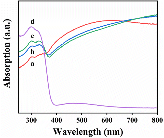 | ||
| Fig. 5 UV-vis diffuse reflectance spectrum of TiO2/Ti3C2 at different reaction stages: (a) 4 h, (b) 8 h, (c) 12 h, and (d) 16 h, respectively. | ||
3.2 Biosensing performances testing
Several PEC performances testing of Ti3C2, TiO2, and TiO2/Ti3C2 were recorded, including photocurrent responses and electrochemical impedance spectroscopy (EIS) (Fig. 6). EIS spectrum is made up of semicircle and linear component, which respectively represent the process of electron transfer and diffusion being restricted. The semicircle diameter in the high frequency region is related to the electron transfer impedance. In Fig. 6(A), the photocurrent of pure anatase TiO2 was about 6.16 μA. After Ti3C2 nanoflakes were loaded, the photocurrent of TiO2/Ti3C2 composite reached 20.21 μA, which was 3.28 times as large as that of bare TiO2 at the bias voltage of 0 V. When the light reached the TiO2 surface, the electrons could be diverted swiftly to Ti3C2, which effectively accelerated the charge transfer. Accordingly, the photoelectric response and its absorption performance were improved. The reason for this result was the introduction of Ti3C2 nanoparticles, which closely connected the separated TiO2. Thus, the electron transfer rate could be increased, and the recombination of electron–hole pairs could be effectively suppressed, as shown in Fig. 6(B). Another reason was that the accordion shape of Ti3C2 greatly increased the superficial area of TiO2, which provided more active sites for photoelectricity.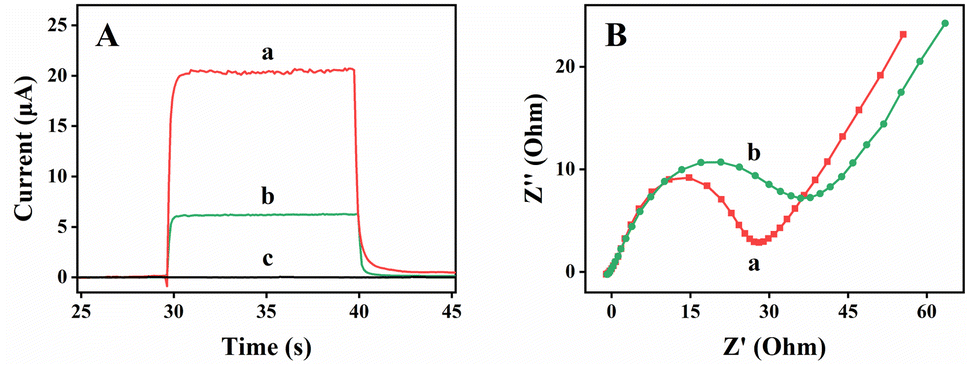 | ||
| Fig. 6 (A) Photocurrent responses and (B) EIS of (a) TiO2/Ti3C2 composite, (b) TiO2, and (c) Ti3C2. | ||
Hydrothermal time condition was optimized for effective application to target DNA detection. Fig. 7(A) shows the response of different hydrothermal time. A line diagram was made accordingly, as shows from Fig. 7(B), to display the respective response values more intuitively. The maximum value was reached at 12 h, which might be due to the increase in the amount of PEC active materials with the rise in the hydrothermal oxidation time of TiO2/Ti3C2, which caused an increment in photocurrent. However, the PEC response decreased with the further increase in hydrothermal oxidation time after 12 h. This finding might be due to that the diffusion to hinder electron movement increased. As shown in Fig. S2,† anatase TiO2 peak was not observed at about 25° for the heterojunction structure at 4 and 8 h. However, a small amount of TiO2 could be observed in Figs. S3(A) and (B).† This result might be due to too little TiO2. Thus, it could not be displayed on the XRD. As showed in Fig. S3,† the results showed that TiO2 gradually increased with time, and the accordion-like Ti3C2 could barely be observed. Therefore, we chose 12 h as the best hydrothermal reaction time.
 | ||
| Fig. 7 TiO2/Ti3C2 composite at different hydrothermal times of (A) photocurrent responses and (B) corresponding line diagram: (a) 4 h, (b) 8 h, (c) 12 h, and (d) 16 h, respectively. | ||
Different CdSe QD concentrations and hybridization times were tested, as showed in Fig. 8. The concentration of QDs also greatly influenced the detection process. As showed in Fig. 8(A), the response first increased with the rise in concentration, reached a peak, and started to descend. Thus, the concentration of 6 μM was the optimal value for this experiment. Fig. 8(B) shows that, with the increase in reaction time, the response of the photocurrent signal declined until it reached its lowest value within 50 min, which suggested that the target DNA had completely combined with probe DNA at this point. Consequently, 50 min was chosen as the perfect hybridization time.
 | ||
| Fig. 8 Influence of (A) CdSe QD concentration and (B) hybridization time with probe DNA on the PEC response. | ||
Photoelectrochemical testing on the signal response of the electrode in different modification steps were conducted, including photocurrent responses and EIS. First, the photocurrent responses were conducted. As observed in Fig. 9(A), the PEC response of FTO/TiO2/Ti3C2 electrode was about 20 μA (curve a). However, after AuNPs were deposited, the photocurrent went down slightly (curve b, I = 18 μA).46,47 This result was probably due to the existence of Schottky effect and surface plasmon resonance effect (SPR) in the full spectrum range, and the Schottky effect is dominant. The Fermi energy level of TiO2 was higher than that of AuNPs. Therefore, some photogenerated electrons would flow from TiO2 to AuNPs to balance this state. When probe DNA was smoothly loaded on the modified electrode, this situation changed and the response slightly increased (curve c, I = 19 μA).46 As mentioned earlier, probe DNA weakened the imbalance relationship between Fermi energy levels, which resulted in an improved photoelectric signal. With the modification of CdSe QDs on the surface of electrode, the PEC response increased rapidly and reached to 29 μA (curve d). It could be explained by that the sensitization of CdSe QDs accelerated the charge transfer and improved the response. When the modified electrode was incubated with the target DNA, the photocurrent signal response was reduced to 24 μA (curve e). The reason was that the probe DNA formed into a rigid DNA double strand after the target DNA was hybridized with the probe DNA. Meanwhile, CdSe QDs were far away from the surface of the electrode, and the electrons on CdSe QDs could not be transferred to TiO2, resulting in a decrease in photocurrent signals.
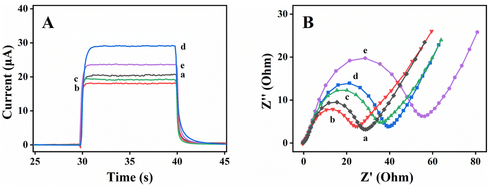 | ||
| Fig. 9 (A) Corresponding photocurrent responses and (B) EIS of every modification steps: (a) FTO/TiO2/Ti3C2, (b) FTO/TiO2/Ti3C2/AuNPs, (c) FTO/TiO2/Ti3C2/AuNPs/probe DNA, (d) FTO/TiO2/Ti3C2/AuNPs/probe DNA/CdSe QDs, and (e) FTO/TiO2/Ti3C2/AuNPs/probe DNA/CdSe QDs/target DNA. | ||
EIS was used for monitoring to further verify the rationality of sensor assembly. Fig. 9(B) shows the EIS spectra of the gradually modified electrode. The electrode of FTO/TiO2/Ti3C2 displayed a relatively petty charge transfer impedance (curve a). When AuNPs were loaded on the surface of the modified electrode, the electron transfer impedance was diminished significantly (curve b). This finding might be due to the excellent electronic conductivity of AuNPs. However, after the gradual incubation of probe DNA fixation (curve c), CdSe QDs (curve d), and MCH termination and DNA hybridization curve (e), the resistance of electron transfer had continued to increase. This result could be attributed to the low conductivity of probe DNA and static electricity exclusion negatively charged ions and Fe(CN)63−/4− in the solution, which weakened the charge transfer. After the target DNA was incubated, the resistance increased, which indicated that it had been successfully combined with probe DNA. The EIS test results were consistent with the PEC measurement results, which confirmed that the DNA sensor had been successfully prepared.
The PEC signal response was closely related to the concentration of DNA. PEC signal current at different DNA concentrations was recorded. The signal level of hybridization between probe DNA and target DNA loaded with diverse target DNA concentrations after modified electrode was observed in the Fig. 10(A). With the increase in DNA concentration from 10 nM to 10 fM, the corresponding photocurrent signal response increased. As showed in Fig. 10(B), each concentration was tested three times and averaged, and the standard deviation was calculated respectively to get the fitting curve with the error bar. The regression equation was I (μA) = 14.22 + 0.407![[thin space (1/6-em)]](https://www.rsc.org/images/entities/char_2009.gif) logCT-DNA/pM (S/N = 3) and the linear correlation coefficient was 0.996. The sensor of this preparation method was contrasted with other accepted sensors. The detection range of target DNA in this study was wider and the limit of detection was lower, as showed in Table S2.†
logCT-DNA/pM (S/N = 3) and the linear correlation coefficient was 0.996. The sensor of this preparation method was contrasted with other accepted sensors. The detection range of target DNA in this study was wider and the limit of detection was lower, as showed in Table S2.†
 | ||
| Fig. 10 (A) Biosensors response to PEC of different concentration targets, (B) calibration curve (C) stability of the PEC biosensor with 1 nM target DNA, and (D) selectivity and specificity of the constructed PEC DNA sensor for different targets, including (a) blank group, (b) one base mismatch, (c) completely mismatch, (d) a mixture (containing 1 nM of one base mismatch, completely mismatch, and 0.1 nM of target DNA), and (e) 0.1 nM of target DNA. | ||
Stability is a critical indicator to test the constructed method. To investigate the long-term stability of PEC biosensor, the modified electrode, which had been incubated with 1 nM target DNA, was examined by 9 intervals of photocurrent responses after being placed for 5 weeks. The test solution was 0.1 M PBS containing 0.1 M AA (pH = 7.4). As shown in Fig. 10(C), the PEC signal remained at about 93% after 5 weeks of storage at 4 °C in the refrigerator. It also showed a stable and repeatable photocurrent, which indicated that the PEC sensor based on TiO2/Ti3C2 heterostructure had good stability. The PEC sensor had unique selectivity for target DNA, as shown in Fig. 10(D). The selectivity of PEC platform was studied with 1 nM one base mismatch DNA, base completely mismatch, and a mixture with 1 nM of one base mismatch, base completely mismatch, and 0.1 nM of target as interfering agents. The figure shows that the target DNA response was far lower than the signal of other interferences, which implied that the constructed detection strategy was feasible and had good anti-interference ability.
3.3 Charge transfer mechanism
In order to determine the energy levels positions of TiO2, Ti3C2 and TiO2/Ti3C2, tests were carried out by Mott–Schottky plots. As shown in the Fig. 11 (A) to Fig. 11 (C), the intersection point of the three dotted lines and the abscissa was the flat-band potential of TiO2 at −0.88 V (relative to Ag/AgCl). Similarly, the Fermi energy level abscissa intercept of Ti3C2 was −1.39 V (relative to Ag/AgCl), and that of TiO2/Ti3C2 was −0.94 V (relative to Ag/AgCl). Therefore, the Fermi energy level of Ti3C2 was below that of TiO2. As shown in Scheme 1, when the target DNA was not present in the detection system, the electron transfer route of TiO2/Ti3C2 and CdSe QDs are shown in Fig. 11(D). The conduction band (CB) of CdSe QDs was higher than TiO2, so the photogenerated electrons would migrate from the CB of CdSe QDs to TiO2 and aggregate with the electrons generated by the TiO2 itself. In addition, when there was target DNA, the probe DNA formed a rigid double stranded DNA with the target DNA, forcing CdSe QDs to move away from the electrode surface, making it impossible for electrons on the CB of CdSe QDs transfer to TiO2. Meanwhile, the electrons in TiO2 jumped from its valence band (VB) to the CB and created holes in the VB under light irradiation. Electrons in the CB of TiO2 could move to Ti3C2, and the existence of Schottky interface further accelerated the carrier separation.48 As a result, the electrons could effectively transfer and separate with the help of TiO2/Ti3C2. | ||
| Fig. 11 Mott–Schottky curves of (A) TiO2, (B) Ti3C2, (C) TiO2/Ti3C2, and (D) Electron transfer mechanism over the TiO2/Ti3C2 and CdSe QDs PEC system. | ||
4 Conclusions
In conclusion, the TiO2/Ti3C2 heterojunction structure was prepared by hydrothermal oxidation method and successfully used as a PEC sensing substrate material for the detection of DNA. The composition and structure of the composite material were characterized by XRD, SEM, TEM, XPS, and UV-vis techniques. Owing to the sufficiently wide area range and plentiful active positions of TiO2/Ti3C2 composites, the re-integration of photogenerated electron–hole pairs was greatly restrained, and the charge transfer to the surface of composite was accelerated. The biosensor exhibited more excellent sensitivity and higher photoelectric response than pure TiO2 because of its large specific surface area. The photocurrent of TiO2/Ti3C2 composite was 3.28 times that of bare TiO2, and the light absorption range extended from UV epitaxy to visible light. The detection range was from 10 nM to 10 fM, with a lower limit of detection 6 fM. The prepared PEC DNA also possessed excellent selectivity, remarkable sensitivity, and high stability. It had positive clinical diagnostic latent capacity in the detection of target DNA.Author contributions
Caiyan Lai: conceptualization, data management, examination, methodology, writing – draft. Mingyu Wang, Heyu He and Jinchun Tu revised the manuscript. All authors had given approval to the final version of the manuscript.Conflicts of interest
There are no conflicts to declare.Acknowledgements
This research was financially supported by the Hainan Province Science and Technology Special Fund (No. ZDYF2021SHFZ068), the National Natural Science Foundation of China (No. 52262014), the Hainan Provincial Natural Science Foundation of China (No. 823CXTD376), CAMS Innovation Fund for Medical Sciences (No. 2019-I2M-5-023), Key Laboratory Open Project Fund of Emergency and Trauma of Ministry of Education (No. KLET-202008).Notes and references
- M. Luan, L. Yu, Y. Li, W. Pan, X. Gao, X. Wan, N. Li and B. Tang, Anal. Chem., 2017, 89, 10601–10607 CrossRef CAS PubMed.
- S. Zhai, C. Fang, J. Yan, Q. Zhao and Y. Tu, Anal. Chim. Acta, 2017, 982, 62–71 CrossRef CAS PubMed.
- M. N. Islam, V. Gopalan, M. H. Haque, M. K. Masud, M. S. A. Hossain, Y. Yamauchi, N.-T. Nguyen, A. K.-Y. Lam and M. J. A. Shiddiky, Biosens. Bioelectron., 2017, 98, 227–233 CrossRef CAS PubMed.
- G. Wen, X. Yang and Y. Wang, J. Mater. Chem. B, 2017, 5, 7775–7780 RSC.
- H. Wang, P. Liu, W. Jiang, X. Li, H. Yin and S. Ai, Sens. Actuators, B, 2017, 244, 458–465 CrossRef CAS.
- J. Huang, X.-Y. Li, Y.-C. Du, L.-N. Zhang, K.-K. Liu, L.-N. Zhu and D.-M. Kong, Biosens. Bioelectron., 2017, 91, 417–423 CrossRef CAS PubMed.
- X. Xu, A. Makaraviciute, S. Kumar, C. Wen, M. Sjödin, E. Abdurakhmanov, U. H. Danielson, L. Nyholm and Z. Zhang, Anal. Chem., 2019, 91, 14697–14704 CrossRef CAS PubMed.
- L. Zhao, R. Sun, P. He and X. Zhang, Anal. Chem., 2019, 91, 14773–14779 CrossRef CAS PubMed.
- J. Li, X. Weng, F. Mo, M. Han and H. Li, Anal. Chem., 2020, 92, 15145–15151 CrossRef CAS PubMed.
- X. Tang, D. Zhao, J. He, F. Li, J. Peng and M. Zhang, Anal. Chem., 2013, 85, 1711–1718 CrossRef CAS PubMed.
- S. J. Hurst, M. S. Han, A. K. R. Lytton-Jean and C. A. Mirkin, Anal. Chem., 2007, 79, 7201–7205 CrossRef CAS PubMed.
- H. Zhang, Y. Yang, H. Dong and C. Cai, Biosens. Bioelectron., 2016, 86, 927–932 CrossRef CAS PubMed.
- Z. Li, X. Ding, K. Yin, Z. Xu, K. Cooper and C. Liu, Biosens. Bioelectron., 2021, 192, 113498 CrossRef CAS PubMed.
- Y. Zhao, L. Tan and G. Jie, Sens. Actuators, B, 2021, 333, 129586 CrossRef CAS.
- L. Yang, X. Zhou, K. Zhang, J. Liu, L. Zhao, A. Cai, X. Zhao, L. Wu and Y. Qin, Sens. Actuators, B, 2023, 382, 133490 CrossRef CAS.
- J. Shu and D. Tang, Anal. Chem., 2020, 92, 363–377 CrossRef CAS PubMed.
- Z. Qiu, J. Shu and D. Tang, Anal. Chem., 2018, 90, 1021–1028 CrossRef CAS PubMed.
- B. Wang, Y.-X. Dong, Y.-L. Wang, J.-T. Cao, S.-H. Ma and Y.-M. Liu, Sens. Actuators, B, 2018, 254, 159–165 CrossRef CAS.
- Y. Wang, P. Wang, Y. Wu and J. Di, Sens. Actuators, B, 2018, 254, 910–915 CrossRef CAS.
- B. Zhang, Y. Lu, C. Yang, Q. Guo and G. Nie, Biosens. Bioelectron., 2019, 134, 42–48 CrossRef CAS PubMed.
- Y. Qu and X. Duan, Chem. Soc. Rev., 2013, 42, 2568–2580 RSC.
- W.-W. Zhao, J.-J. Xu and H.-Y. Chen, Chem. Soc. Rev., 2015, 44, 729–741 RSC.
- H. Li, M. Zhu, S. Wang, W. Chen, Q. Liu, J. Qian, N. Hao and K. Wang, J. Mater. Chem. B, 2017, 5, 8999–9005 Search PubMed.
- X. Yan, J. Li, R. Yang, Y. Li, X. Zhang and J. Chen, Sens. Actuators, B, 2018, 255, 2187–2193 CrossRef CAS.
- Y.-J. Li, M.-J. Ma and J.-J. Zhu, Anal. Chem., 2012, 84, 10492–10499 CrossRef CAS PubMed.
- A. Meng, L. Zhang, B. Cheng and J. Yu, Adv. Mater., 2019, 31, 1807660 CrossRef PubMed.
- X. Wang, P. Gao, T. Yan, R. Li, R. Xu, Y. Zhang, B. Du and Q. Wei, Sens. Actuators, B, 2018, 258, 1–9 CrossRef CAS.
- Z. Zeng, Y.-B. Li, S. Chen, P. Chen and F.-X. Xiao, J. Mater. Chem. A, 2018, 6, 11154–11162 RSC.
- Y. Pang, W. Zang, Z. Kou, L. Zhang, G. Xu, J. Lv, X. Gao, Z. Pan, J. Wang and Y. Wu, Nanoscale, 2020, 12, 4302–4308 RSC.
- H. Xu, A. Ren, J. Wu and Z. Wang, Adv. Funct. Mater., 2020, 30, 2000907 CrossRef CAS.
- W. Zhou, J. Zhu, F. Wang, M. Cao and T. Zhao, Mater. Lett., 2017, 206, 237–240 CrossRef CAS.
- M. Ghidiu, M. R. Lukatskaya, M. Q. Zhao, Y. Gogotsi and M. W. Barsoum, Nature, 2014, 516, 78–81 CrossRef CAS PubMed.
- I. Ihsanullah, J. Environ. Chem. Eng., 2022, 10, 107381 CrossRef CAS.
- Y. Wei, P. Zhang, R. A. Soomro, Q. Zhu and B. Xu, Adv. Mater., 2021, 33, 2103148 CrossRef CAS PubMed.
- Z. Li and Y. Wu, Small, 2019, 15, 1804736 CrossRef PubMed.
- C. Peng, X. Yang, Y. Li, H. Yu, H. Wang and F. Peng, ACS Appl. Mater. Interfaces, 2016, 8, 6051–6060 CrossRef CAS PubMed.
- C. Chen, X. Zhou, Z. Wang, J. Han and S. Chen, Anal. Chim. Acta, 2022, 1216, 339943 CrossRef CAS PubMed.
- V. Kamysbayev, A. S. Filatov, H. Hu, X. Rui, F. Lagunas, D. Wang, R. F. Klie and D. V. Talapin, Science, 2020, 369, 979–983 CrossRef CAS PubMed.
- N. Lu, X. Hu, J. Jiang, H. Guo, G. Z. Zuo, Z. Zhuo, X. Wu and X. C. Zeng, Nanoscale, 2023, 15, 4821–4829 Search PubMed.
- D. Su, S. Dou and G. Wang, Chem. Mater., 2015, 27, 6022–6029 CrossRef CAS.
- L. Li, G. Jiang, C. An, Z. Xie, Y. Wang, L. Jiao and H. Yuan, Nanoscale, 2020, 12, 10369–10379 RSC.
- Z. Huang, Q. Zeng, Y. Liu, Y. Xu, R. Li, H. Hong, L. Shen and H. Lin, J. Membr. Sci., 2021, 640, 119854 CrossRef CAS.
- S. Lu, S. Yang, X. Hu, Z. Liang, Y. Guo, Y. Xue, H. Cui and J. Tian, Int. J. Hydrogen Energy, 2019, 44, 24398–24406 CrossRef CAS.
- A. Saeed, W. Chen, A. H. Shah, Y. Zhang, I. Mehmood and Y. Liu, J. CO2 Util., 2021, 47, 101501 CrossRef CAS.
- H. Shi, J. Chen, G. Li, X. Nie, H. Zhao, P.-K. Wong and T. An, ACS Appl. Mater. Interfaces, 2013, 5, 6959–6967 CrossRef CAS PubMed.
- X. P. Liu, J. S. Chen, C. J. Mao, H. L. Niu, J. M. Song and B. K. Jin, Biosens. Bioelectron., 2018, 116, 23–29 CrossRef CAS PubMed.
- J. Prakash, S. Sun, H. C. Swart and R. K. Gupta, Appl. Mater. Today, 2018, 11, 82–135 CrossRef.
- Y. Liu, Y.-H. Li, X. Li, Q. Zhang, H. Yu, X. Peng and F. Peng, ACS Nano, 2020, 14, 14181–14189 CrossRef CAS PubMed.
Footnote |
| † Electronic supplementary information (ESI) available: Specific oligonucleotide sequences; comparison of different sensors for the detection of target DNA; TEM image and SEAD of CdSe QDs; XRD patterns of TiO2/Ti3C2 prepared for different reaction times; SEM images of TiO2/Ti3C2 prepared for different reaction times. See DOI: https://doi.org/10.1039/d3ra02100a |
| This journal is © The Royal Society of Chemistry 2023 |