
 Open Access Article
 This Open Access Article is licensed under a Creative Commons Attribution-Non Commercial 3.0 Unported Licence
Growth of nanostructured Cu3Al alloy films by magnetron sputtering for non-enzymatic glucose-sensing applications†
Yuqing Yina,
Ting Zhanga,
Lemeng Fengb,
Junhui Rana,
Chao Maa,
Yongwen Tan a,
Weitao Song*b and
Bin Yang*a
a,
Weitao Song*b and
Bin Yang*a
aCollege of Materials Science and Engineering, Hunan University, Changsha, 410082, China. E-mail: yangb1@hnu.edu.cn
bXiangya Hospital of Central South University, Changsha, 410008, China. E-mail: wtsong1980@csu.edu.cn
First published on 19th May 2023
Abstract
Enzymatic glucose sensors usually exhibit excellent sensitivity and selectivity but suffer from poor stability due to the negative influence of temperature and humidity on enzyme molecules. As compared to enzymatic glucose sensors, non-enzymatic counterparts are generally more stable but are facing challenges in concurrently improving both sensitivity and selectivity of a trace amount of glucose molecules in physiological samples such as saliva and sweat. Here, a novel non-enzymatic glucose sensor based on nanostructured Cu3Al alloy films has been fabricated by a facile magnetron-sputtering followed by controllable electrochemical etching approach. Since the metal Al is more reductive than Cu, by selectively etching aluminum in the Cu3Al alloys, nanostructured alloy films were obtained with increased surface contact area and electrocatalytic active sites which resulted in enhanced glucose-sensing performance. Thus, non-enzymatic glucose sensors based on nanostructured Cu3Al alloy films not only exhibited a high sensitivity of 1680 μA mM−1 cm−2 but also achieved a reliable selectivity to glucose without interference by other species in physiological samples. Consequently, this study sparked the potential for the development of non-enzymatic biosensors for the continuous monitoring of blood glucose levels with high sensitivity and impressive selectivity for glucose molecules.
1. Introduction
Diabetes, caused by defective insulin secretion or action, is one of the three major chronic diseases that can seriously affect human health, leading to numerous complications, such as hypertension, stroke, kidney failure, and heart disease.1,2 It is urgently demanded to develop an efficient, reliable, inexpensive and mild blood glucose testing technology for long-term health-management of both diabetic and non-diabetic individuals. Multiple strategies, including optical,3,4 calorimetric,5 mass spectrometry,6 and electrochemical,7,8 have been proposed to precisely monitor the variation of blood glucose level. Due to the advantages of high sensitivity and fast response, growing attention has been paid to electrochemical glucose sensors.9 Electrochemical glucose sensors are generally categorized into enzymatic-based and non-enzymatic groups. Enzymatic glucose sensors usually exhibit excellent selectivity, but their stability is often compromised by the negative effects of temperature and humidity on enzyme degradation.10 Non-enzymatic glucose sensors are primarily based on nanostructured electrodes, which can offer better environmental stability and enable continuous monitoring of blood glucose level due to the absence of unstable enzymes.11–13The key to the development of non-enzymatic glucose sensors is the development of nanostructured electrodes which can effectively facilitate the electro-chemical oxidation process on their surfaces without the use of electron-transfer mediators, such as Prussian blue, which are typically employed in their enzymatic counterparts. Typically, the nanostructured electrodes are made of conductive materials, including carbon graphite, precious metals (e.g. Au,14 Pt,15 Pd16), non-precious metals (e.g. Cu,17 Ni18), and metal alloys (e.g. Pt–Pb,19 Au–Ni,20 Pt–Au21). Among them, alloys have attracted more attentions due to the potential of achieving superior glucose-sensing performance by tuning their chemical composition and modulating film morphology to increase the binding energy of surface absorbed hydroxyl groups and enriched active sites for fast electro-oxidation kinetics of glucose on the alloy surface.22–26
As compared to costly precious metals such as Au, Pt, and Pd, the non-precious metal Cu has been extensively applied in electrochemical devices due to its low price, easy availability, non-toxicity, and excellent catalytic activity. However, the electrochemical performance of individual Cu metal is still limited so that doping previous metals (e.g. Pd) into Cu can improve the glucose sensing performance.27–29 Existing studies have shown that doping of metal atoms in matrix materials can significantly enhance the electrocatalysis or photocatalysis of the materials,30,31 which can be attributed to the fact that the doping of heteroatoms altered the grain size, electronic structure, band gap energy or active sites of the crystal.32–34 As a consequence, it is of great importance to find an inexpensive alternative to the previous metals to doping Cu to improve the electrochemical performance and reduce the fabrication cost of glucose sensors.
In this work, we first employed a novel Cu3Al alloy film electrode prepared by the combination of magnetron sputtering and electrochemical etching in the construction of non-enzymatic glucose sensors. The composition and surface morphology of the thin film electrode were regulated by changing the content of Al atoms doped into the Cu matrix, and the Cu3Al alloy thin film was prepared when the Al atoms were doped at 25%. Subsequently, the surface of the Cu3Al alloys was selectively etched to deliver a nanostructured electrode for fabricating high-performance non-enzymatic glucose sensor. Specifically, the Al component was selectively etched as it is relatively reactive to a sodium hydroxide (NaOH) solution. Therefore, the nanostructured Cu on the surface of the Cu3Al alloy can be utilized as a catalyst to promote electrochemical oxidation of glucose. The glucose sensing performance was optimized by changing the NaOH concentration and etching time, the resultant non-enzymatic glucose sensor exhibited a high sensitivity of 1680 μA mM−1 cm−2 with an ultra-low detection limit of 0.22 μM (S/N = 3) along with a linear range from 2 μM to 10 mM.
2. Experimental
2.1 Materials
D-(+)-glucose (≥99.5%), uric acid (UA), urea (UR), and L-ascorbic acid (AA) were purchased from Sigma Aldrich. NaOH particles (≥96%) were received from Xilong Scientific. Hyaluronic acid (HA) was ordered from Tokyo Chemical Industry, and lactic acid was purchased from Acros Organics. Silicon wafers were obtained from Shunsheng Electronics Co. All chemicals were used as received without any further purification. Ultrapure water was used in all experiments. Both Al (99.999%) and Cu (99.995%) targets were provided by ZhongNuo Advanced Material Technology Co.2.2 Fabrication of Cu–Al alloy films
The Cu–Al film alloy was deposited on a substrate of (100) silicon wafer with a magnetron-sputtering system (TRP450, Sky Technology Development Co.), where a Cu target was mounted onto a RF power supply and an Al target on a DC power supply. The alloy composition was tuned by changing both the sputtering power and the target-base distance for Cu and Al targets, respectively.35,36 Argon was used as the working gas under a working pressure of 0.3 Pa and a fixed flow rate of 40 sccm. The substrate was not heated, and it rotated at 5 rpm. The thickness of the alloy films was about 1.06 μm. Finally, the as-prepared Cu–Al alloy films were electrochemically etched in NaOH solution to remove Al component, leaving a porous nanostructure on their surface.2.3 Characterization of Cu–Al alloy films and sensors
Scanning electron microscopy (SEM, Helios NanoLab G3 UC) with energy-dispersive spectroscopy (EDS), atomic force microscopy (AFM, Bruker Dimension Icon) and high-resolution transmission electron microscopy (HRTEM, Themis Z) were employed to obtain morphological images and elemental distribution in the Cu–Al alloy films. X-ray diffraction (XRD, Mini flex 600) with Cu Kα irradiation (λ = 1.5406 Å) from 10° to 90° in steps of 0.02° and X-ray photoelectron spectroscopy (XPS, AXIS SUPRA+) were applied to analyze the chemical and elemental information of the Cu–Al films. The electrodes and their glucose-sensing performance were characterized by an electrochemical workstation (VERTEX. Ivium Technologies BV Co.) with a conventional three-electrode system where the Ag/AgCl electrode, the Pt foil and the Cu–Al film alloy were used as the reference, counter, and working electrodes, respectively. The reference Ag/AgCl electrode was used as received without any further calibration. The glucose sensing performance of prepared electrode was evaluated by cyclic voltammetry (CV) between −1.2 V and 1.2 V at a scan rate of 50 mV s−1 in a stationary solution, and chronoamperometry (CA) at 0.5 V in a magnetically stirred solution.3. Results and discussion
3.1 Magnetron-sputtering Cu–Al alloy films
The Cu–Al film alloys were co-deposited on silicon wafers by magnetron sputtering equipped with a Cu target and an Al target, the synthesis diagram was illustrated in Fig. 1. Both the alloy composition and surface appearance can be tuned by changing the sputtering parameters. | ||
| Fig. 1 Synthesis diagram of Cu–Al alloy film. | ||
Scanning electron microscopy was used to demonstrate the surface topography of the pure Cu, pure Al, and Cu–Al alloy films. As shown in Fig. 2a and b, the cubic nanoparticles with an average size of 30 nm were observed in the sputtered-Cu film, while the pure Al film was composed of larger irregular particles with an average size of 88 nm. As loading a small amount of Al into the Cu matrix (Fig. 2c), the average grain size increased significantly to 250 nm. The statistical distribution of particle size of these as-prepared films was shown in Fig. S1.† The EDS spectra were collected to examine the Cu and Al composition ratio of the alloy (Fig. S2†), revealing that the content of Al atoms in the prepared Cu–Al films in Fig. 2c–f was 8%, 13%, 25% and 40%, respectively. This result is consistent with the observation of color change from brown to gray with increasing Al ratio. More interestingly, by introducing more Al atoms into the Cu matrix (Fig. 2c–f), the Cu–Al alloys exhibited a distinct morphological change and an apparent decrease in grain sizes, suggesting a possible change in crystal orientation and/or formation of new phases.
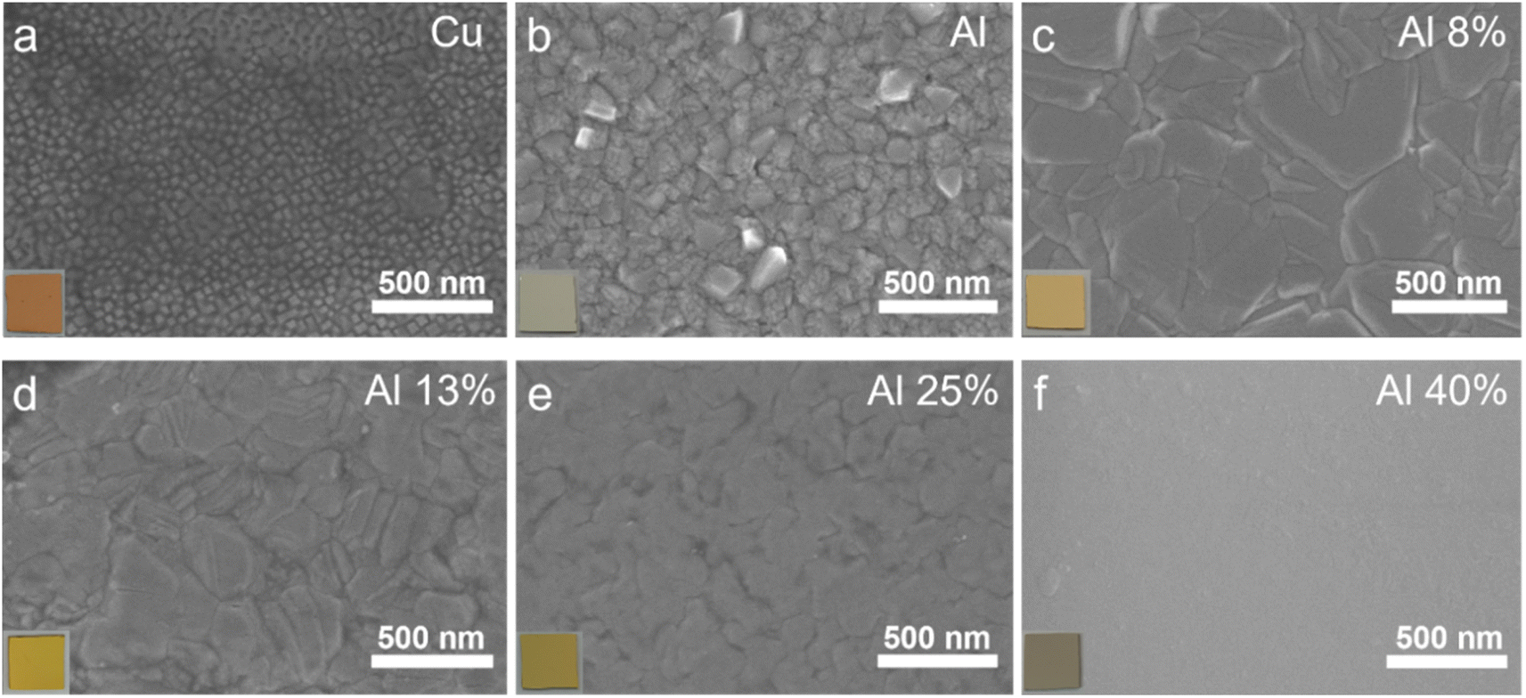 | ||
Fig. 2 Morphological variation as a function of Cu![[thin space (1/6-em)]](https://www.rsc.org/images/entities/char_2009.gif) :Al composition ratio revealed by SEM images: (a) Cu, (b) Al, (c) Al 8%, (d) Al 13%, (e) Al 25% and (f) Al 40%. The inset showing photographs of real film alloys (1 × 1 cm2). :Al composition ratio revealed by SEM images: (a) Cu, (b) Al, (c) Al 8%, (d) Al 13%, (e) Al 25% and (f) Al 40%. The inset showing photographs of real film alloys (1 × 1 cm2). | ||
In order to determine phase structure of the as-prepared Cu–Al alloys, their respective X-ray diffraction (XRD) patterns were collected as shown in Fig. 3a. For the pristine Cu film samples, three characteristic peaks were located at 43.3°, 50.5° and 74.3°, which were assigned to the (111), (200) and (220) crystal planes of cubic (FCC) Cu (JCPDS card no. 04-0836), respectively. Referring to the standard PDF card of cubic (FCC) Al (JCPDS card no. 04-0787), the diffraction peaks at 38.5°, 44.7° and 65.1° represented the (111), (200) and (220) planes of Al crystals, respectively. It can be seen that the XRD patterns of the films obtained by co-sputtering Cu and Al targets differ from those of pure Cu and Al metals. According to the equilibrium phase diagram of Cu–Al alloys,37 no alloy phase was generated when the Al atomic content was 8% and 13%, but the Cu and Al bimetallic composite films exhibited a preferred orientation along the (111) plane of Cu. With further increasing Al atomic content to 25%, a new alloy phase of Cu3Al was formed, as indicated by XRD measurements. The XRD peaks located at 40.0° and 42.7° were assigned to the (202) and  crystal planes of Cu3Al (JCPDS card no. 28-0005). It was accompanied by a number of other diffraction peaks from monometallic Cu and Al metals as a result of incomplete reaction of Cu and Al during the magnetron sputtering process. When the Al atomic content was further increased to 40%, the XRD peaks at 35.7°, 49.2° and 74.0° correspond to the (222), (332), (631) planes of Cu9Al4 (JCPDS card no. 24-0003), while the other peaks are attributed to Cu3Al2 (JCPDS card no. 26-0015). Moreover, high-resolution TEM revealed that the alloy film with Al 25% was composed of nanoparticles as shown in Fig. 3b. The lattice fringe in the Al 25% film was estimated to be 0.211 nm (Fig. 3c), which corresponds to the
  plane of Cu3Al. Additionally, as shown in Fig. 3d, two concentric rings in the selected area electron diffraction (SAED) image signifies the existence of the
  plane of Cu3Al and (200) plane of Cu. These observations are consistent with the XRD results, clearly indicating the successful formation of Cu3Al alloys.
 | ||
| Fig. 3 Structural and composition analysis: (a) XRD patterns of as-prepared Cu (orange), Al (dark) and different Al composition ratio in the Cu–Al films: 8% (green), 13% (pink), 25% (blue) and 40% (purple); (b and c) HRTEM images of Al 25% alloy sample with different magnifications; (d) SAED pattern of Al 25%; XPS spectra of (e) Cu 2p, (f) Al 2p. | ||
To further distinguish the valence states of both Cu and Al in the alloys, X-ray photoelectron spectroscopy (XPS) spectra were obtained from a representative sample of Al 25% (Cu3Al), and characteristic spectral peaks of Cu and Al elements were shown in Fig. S3.† Fig. 3e showed the Cu 2p spectrum, where the spectral peaks at 932.1 and 952.0 eV were assigned to Cu0 2p3/2 and Cu0 2p1/2, respectively.38 The other peaks at 934.6 and 954.4 eV indicated oxidization of Cu on the alloy surface.39 As shown in Fig. 3f, the XPS peak at 72.1 eV was assigned to metallic Al, and the strong peaks at 74.3 and 76.4 eV were attributed to AlOx and Al3+ (e.g. Al2O3 or Al(OH)3), respectively.40,41 In addition to forming of Cu–Al alloys, both Cu and Al on the alloy surface also oxidized when stored in the ambient environment.
3.2 Electro-chemical oxidation of glucose on Cu–Al alloys
The CV data were utilized to evaluate the electrocatalytic oxidation performance of the as-prepared Cu–Al alloys on the glucose molecules in the potential range from −1.2 to 1.2 V. CV measurements of the Al 25% (Cu3Al) alloy as the electrode were carried out in the 0.1 M NaOH solution without and with 5 mM glucose. As shown in Fig. 4a, according to the reported literature,42,43 the oxidation peak at −0.35 V appeared in the anodic scan direction, which was attributed to the oxidation of Cu0 to Cu+, and the peak at −0.13 V represented the transition from Cu0 and Cu+ to Cu2+. Cu3+ was formed at around 0.5 V, while the oxidation peak could not be clearly observed in our data, which is attributed to the fact that the formation of Cu3+ can only be recognized in concentrated NaOH.44 When the potential was greater than 0.6 V, the water electrolysis reaction started and a strong increase in the anode current can be observed. When glucose was loaded into the NaOH solution, a significant oxidation peak was observed between 0.5 and 0.8 V, indicating the excellent electrocatalytic capability of the Cu–Al alloy to oxidize glucose molecules. In the cathodic scanning direction, the small cathodic peak at 0.6 V is due to the reduction of Cu3+ to Cu2+, the Cu2+/Cu3+ redox couple was essential for the electrocatalytic oxidation process of glucose. Gluconolactone is very likely to experience desorption to ensure the redox cycle of the whole electrochemical system. The hydroxyl groups (–OH) absorbed on the Cu–Al alloy surface in the NaOH solution play a crucial role in promoting the oxidation of glucose according to the following process:44–46| Cu + 2OH− → CuO + H2O + 2e− | (1) |
| CuO + H2O → Cu(OH)2 | (2) |
| Cu(OH)2 + OH− → CuOOH + H2O + e− | (3) |
| CuOOH + glucose → CuO + glucolactone | (4) |
 | ||
| Fig. 4 Cyclic voltammetry (CV) characterizations of the as-prepared Cu–Al film alloys. (a) Comparison of CV acquired from Al 25% (Cu3Al) in 0.1 M NaOH solution in the absence and presence of 5 mM glucose; (b) Cu and Cu–Al alloy in the presence of 5 mM glucose; (c) Al 25% with different concentrations of glucose at a scan rate of 50 mV s−1; (d) linear relationship between the oxidation peak current density and the concentration of glucose in (c); (e) CV acquired at different scan rates from 20 to 100 mV s−1 with an interval of 20 mV s−1 for the Al 25% alloy; (f) linear relationship between the oxidation peak current density and the scan rate in (e). | ||
Furthermore, to understand the role of Al in promoting oxidation of glucose, the CV measurements were acquired from both pure Cu and a series of Cu–Al film samples with the addition of 5 mM glucose under the same measurement condition. As compared with pure Cu, the oxidation current of glucose on the alloy electrode was increased significantly, and the Cu3Al alloy showed the greatest electrocatalytic performance for glucose oxidation (Fig. 4b). Such improvement is attributable to either electronic interaction among Cu, Al, CuO, Al2O3, CuOOH and other substances,47 or stronger binding of the hydroxyl group on the alloy surface.24
As shown in Fig. 4c and d, as the glucose concentration increased from 2 mM to 10 mM, the oxidation peak current response of glucose increased linearly with a linearity (R2) of 0.998. Additionally, the influence of scan rate on the catalytic activity of the electrode was also investigated (Fig. 4e and f). The peak current of glucose oxidation progressively increased with increasing scan rate, and it was linearly related to the square root of the scan rate, indicating a favorable current response for the Al 25% alloy. The observation proved a typical diffusion-controlled electrochemical reaction in such glucose oxidation process.48
3.3 Selective-etching Cu3Al alloy films
The surface topography of Cu–Al alloy plays a critical role in obtaining excellent glucose sensing performance. For such consideration, a feasible approach was conducted to increase the surface contact area of the electrode by selectively etching Al in the Cu–Al alloy, as Al is more reactive than Cu in the NaOH solution. This is a typical approach in the dealloying technique, where one component was removed and left with bimetal alloy.47 The schematic diagram of the Cu3Al alloy etched in NaOH solution was shown in Fig. 5.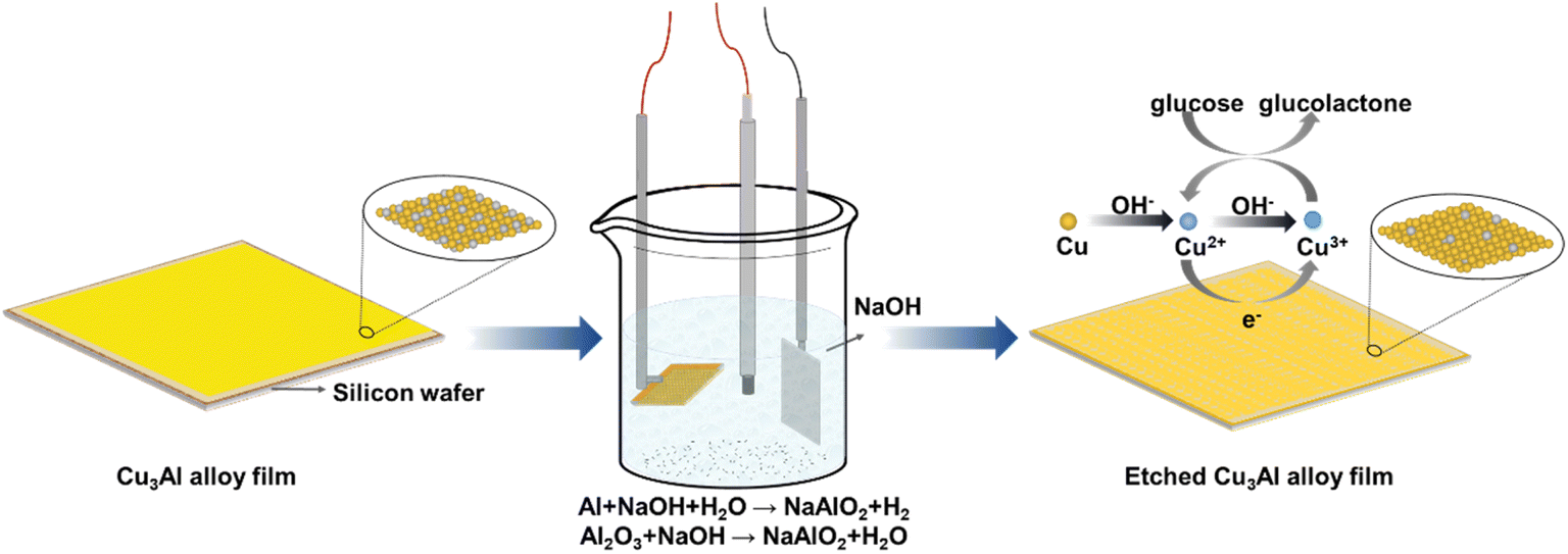 | ||
| Fig. 5 Schematic diagram of the Cu3Al alloy etched in NaOH solution. | ||
In order to enhance the electrochemical catalytic performance of the Cu3Al alloy for glucose, etching parameters were optimized by acquiring amperometric response of stepwise addition of 50 μM glucose in the NaOH solution with changing applied bias, etching time, and NaOH concentration. As shown in Fig. S4,† the current increased significantly with increasing the operating bias, then decreased when the bias was above 0.5 V. Therefore, the operating bias was set at 0.5 V to obtain an excellent current response. The performance as a function of the etching time of Cu3Al alloy in 0.1 M NaOH solution was investigated. Under an applied bias of 0.5 V, it was found that the etching time of 350 s for the electrode exhibited the highest current change in response to the addition of the same amount of glucose (50 μM). Using the optimal applied bias of 0.5 V and etching time of 350 s, we subsequently examined the influence of NaOH solution concentration on electrochemical performance. The alloy electrode showed the highest current response when the NaOH concentration was 0.1 M. By comparing the XRD patterns of the as-prepared and above-etched Cu3Al films (Fig. S5†), we found that the phase structure of the alloy was unchanged after etching. This observation suggests that although the Al atoms on the Cu3Al alloy surface were initially removed by etching with NaOH solution, the leftover Cu atoms were washed-off from the film. Consequently, no additional XRD peak was observed from the etched Cu3Al film.
In order to reveal the variation of surface topography of the Cu3Al alloy films under different etching time and NaOH concentration, six samples of Cu3Al films prepared from the same batch were randomly selected and etched in 0.1 M NaOH solution for 150 s, 350 s, 550 s, and at 0.05 M, 0.5 M, and 1 M NaOH for 350 s, respectively. SEM images were acquired from the as-etched Cu3Al films as shown in Fig. 6. The statistical distribution of particle size of alloy films after changing the etching time was shown in Fig S6.† Fig. 6a showed the original as-prepared electrode, after etching in 0.1 M NaOH solution to remove Al atoms, the alloy films showed a rough crumbling surface morphology with an average grain size of 30 nm when the etching time was 150 s (Fig. 6b). It was noted that the leaf-like morphology was most likely due to the special corrosion behavior of Al during the anodic reaction. With increasing the etching time to 350 s, the Cu3Al grain size of leaf-like structure become 22 nm. This observation agrees well with the XRD result that the leftover Cu atoms were washed-off from the film as discussed above (Fig. 6c). The small leaf-like Cu3Al grains were uniformly distributed on the surface of the alloy electrode, which was expected to increase the specific surface area of the electrode and provide more reactive sites to improve electrochemical performance. When the etching time was further increased to 550 s, the average grain size slightly reduced to 20 nm, but the number of grains on the surface decreased due to the fact that the Cu3Al grains on the electrode surface were further washed-off with over-extended etching time (Fig. 6d).
 | ||
| Fig. 6 SEM images of the Cu3Al alloy after different etching time of (a) 0 s, (b) 150 s, (c) 350 s, (d) 550 s for under the same NaOH concentration of 0.1 M, and different NaOH concentration of (e) 0.05 M, (f) 0.5 M, (g) 1 M under the same etching time of 350 s. | ||
Fig. 6a and e–g showed that the surface topography of Cu3Al alloy varied with different NaOH concentration. The average grain sizes on the electrode surface decreased when the electrolyte concentration increased from 0.05 M to 0.1 M, which was favorable for increasing the active sites of the electrode. When the NaOH concentration was further increased to 0.5 M and 1 M, much larger leaf-like grains were observed in the alloy, most likely due to atomic diffusion induced re-growth of Cu grains during the anodic reaction. Fig. S7† presents the elemental mappings and EDS spectra of Cu3Al alloy after etching, and it is seen that the content of Al atoms on the surface of the alloy was reduced from 25% to 2%, which confirmed the selective etching of Al atoms in the high concentration NaOH solution. By measuring surface roughness with AFM, we found the surface RMS roughness of the electrode was substantially increased from 0.388 nm to 4.63 nm after etching in 0.1 M NaOH solution for 350 s (Fig. S8†). The increase in the specific surface area of the electrode was beneficial in enhancing electrochemical catalytic performance by increasing the efficiency of electron transfer at the interfaces.
3.4 Glucose sensing performance based on Cu3Al alloy electrodes
The J–t curves were investigated to probe glucose oxidation on the surface of a Cu3Al alloy electrode. Fig. 7a showed the typical amperometric response of successive stepwise introduction of different concentrations of glucose in the NaOH solution. It was suggested that the Cu3Al electrode showed an apparent current response to the change in glucose concentration, and the current density displayed a significant linear correlation (R2 = 0.998) with glucose concentration in the range of 2 μM–10 mM as illustrated in Fig. 7b. Such linear response yielded a high sensitivity of 1680 μA mM−1 cm−2 with a low detection limit of 0.22 μM (S/N = 3), and a response time less than 2 s (Fig. 7c). As shown in Table 1, our alloy glucose sensors exhibit the highest sensitivity for the Cu-based materials as compared to those reported in the literature. | ||
| Fig. 7 Glucose sensing performance based on Cu3Al alloy electrodes measured at 0.5 V in 0.1 M NaOH by magnetic stirring: (a) current density–time curves in response to successive addition of glucose in 0.1 M NaOH, (b) linear correlation between the amperometric response and glucose concentration, (c) response time with adding glucose, (d) current response with adding glucose and other interferences with the same amount of 50 μM. | ||
| Modified electrode | Sensitivity (μA mM−1 cm−2) | Detection limit (μM) | Linear range (mM) | Ref. |
|---|---|---|---|---|
| a Abbreviations in this table. PGE: pencil graphite electrode; NPG: nanoporous gold; GP: graphene paper; MOF: metal–organic framework; GC: glassy carbon; NPs: nanoparticles; SPE: screen-printed electrode; ZIF: zeolitic imidazole frameworks; CC: carbon cloth; MWCNTs: multi-walled carbon nanotubes. | ||||
| Cu–Co/rGO/PGE | 240 | 0.15 | 0.001–4 | 49 |
| Nafion/CuO/Au | 1101 | 50 | 0.1–13.3 | 50 |
| PtCo/NPG/GP | 7.84 | 5 | 0.035–30 | 51 |
| Cu-MOF/GC | 89 | 0.0105 | 0.00006–5 | 52 |
| Cu–Ag2O nanowalls/GC | 298.2 | 10 | 0.2–3.2 | 53 |
| CuO/NiO/PANI | — | 2 | 0.02–2.5 | 54 |
| Cu NPs | 412 | 2.76 | 0–0.7 | 55 |
| Cu–Pd/GC | 298 | 0.32 | 0.01–9.6 | 56 |
| SPE/NiCo/C | 265.53 | 0.2 | 0.0005–4.38 | 57 |
| Cu–Ni | 240.1 | — | 0–10 | 58 |
| Cu/Co-ZIF/CC | 1030 | — | 0.05–6 | 59 |
| Co3O4/MWCNTs/Au | 1138.4 | 0.1 | 0.0002–1.1 | 60 |
| Cu/ZnO | 36.641 | 57 | 0.01–1; 1–7 | 61 |
| Cu–Al | 1680 | 0.22 | 0.002–10 | This work |
A reliable glucose biosensor should have the ability to distinguish interferences from the target molecule. In addition to this, it is also essential to assess its selectivity. Apart from glucose, other physiological species, such as hyaluronic acid (HA), urea (UR), lactic acid (LA), uric acid (UA), and L-ascorbic acid (AA), could also be oxidized on the electrode surface, thus interfering with glucose detection. As shown in Fig. 7d, 50 μM glucose, 20 μM HA, UA, AA, and 1 mM LA, UR were added successively into the 0.1 M NaOH solution. It was observed that the addition of glucose resulted in a significant current response (95 μA cm−2), while there was almost no current change when HA, UR and LA were injected and a much weaker response current of 5.9 and 4.1 μA cm−2 was observed due to the introduction of UA and AA, respectively. Although both UA and AA could be oxidized at 0.5 V,62 their weak current response is ascribed to the mutual repulsion between the negatively-charged electrode surface and the negatively-charged interferences (i.e. UA and AA).27 These observations suggest that our non-enzymatic glucose sensors based on Cu3Al alloy films have achieved an excellent selectivity at an applied bias of 0.5 V.
4. Conclusions
In summary, we have obtained nanostructured Cu3Al alloy films which were deposited by magnetron-sputtering as followed by selectively electrochemical etching. The phase structure and grain morphology of Cu–Al alloy films were tunable by changing Al ratio in the Cu matrix. By loading 25% Al into the Cu matrix during the magnetron sputtering process, plane oriented Cu3Al films were achieved. The nanostructure of Cu3Al alloy was further tailored by optimizing the operating bias, etching time and the concentration of NaOH solution in the following electrochemical etching process. The biosensors based on the optimal Cu3Al alloy electrode have exhibited superior glucose detection performance with a high sensitivity of 1680 μA mM−1 cm−2 along with a wide linear range of 2 μM–10 mM and excellent selectivity for sensing glucose. This work offers an economical-efficient magnetron sputtering and selective etching approach to construct nanostructured Cu3Al alloy films which are suitable alternatives to the dominant expensive noble metal films for non-enzymatic glucose-sensing applications.
Author contributions
Yuqing Yin: conceptualization, methodology, formal analysis, writing-original draft; Ting Zhang: conceptualization, methodology, formal analysis; Lemeng Feng: investigation, formal analysis, resources; Junhui Ran: formal analysis, writing-review and editing; Chao Ma: investigation, formal analysis, resources; Yongwen Tan: formal analysis, writing-review and editing; Weitao Song: conceptualization, validation, formal analysis, resources; Bin Yang: conceptualization, validation, formal analysis, resources, writing-review and editing.Conflicts of interest
The authors declare that they have no competing financial interests or personal relationships that could have influenced the work reported in this paper.Acknowledgements
B. Y. acknowledges Research Funds for Central Universities.References
- A. Amer Diabet, Diabetes Care, 2013, 36, S67–S74 CrossRef PubMed.
- X. L. Lin, Y. F. Xu, X. W. Pan, J. Y. Xu, Y. Ding, X. Sun, X. X. Song, Y. Z. Ren and P. F. Shan, Sci. Rep., 2020, 10, 11 CrossRef PubMed.
- M. Z. Yu, K. L. Zhao, X. H. Zhu, S. Y. Tang, Z. Nie, Y. Huang, P. Zhao and S. Z. Yao, Biosens. Bioelectron., 2017, 95, 41–47 CrossRef CAS PubMed.
- V. Zubkovs, N. Schuergers, B. Lambert, E. Ahunbay and A. A. Boghossian, Small, 2017, 13, 10 CrossRef PubMed.
- B. Davaji and C. H. Lee, Biosens. Bioelectron., 2014, 59, 120–126 CrossRef CAS PubMed.
- M. L. Di Gioia, A. Leggio, A. Le Pera, A. Liguori, A. Napoli, C. Siciliano and G. Sindona, J. Chromatogr. B: Anal. Technol. Biomed. Life Sci., 2004, 801, 355–358 CrossRef CAS PubMed.
- H. Lee, T. K. Choi, Y. B. Lee, H. R. Cho, R. Ghaffari, L. Wang, H. J. Choi, T. D. Chung, N. Lu, T. Hyeon, S. H. Choi and D. H. Kim, Nat. Nanotechnol., 2016, 11, 566–572 CrossRef CAS PubMed.
- T. Zhang, J. H. Ran, C. Ma and B. Yang, Adv. Mater. Interfaces, 2020, 7, 9 Search PubMed.
- L. Ding, J. Yan, Z. Zhao and D. Li, Sens. Actuators, B, 2019, 296, 126705 CrossRef CAS.
- S. B. Bankar, M. V. Bule, R. S. Singhal and L. Ananthanarayan, Biotechnol. Adv., 2009, 27, 489–501 CrossRef CAS PubMed.
- J. Zhu, S. B. Liu, Z. H. Hu, X. Z. Zhang, N. Yi, K. R. Tang, M. G. Dexheimer, X. J. Lian, Q. Wang, J. Yang, J. Gray and H. Y. Cheng, Biosens. Bioelectron., 2021, 193, 12 CrossRef PubMed.
- M. Li, L. Liu, Y. Xiong, X. Liu, A. Nsabimana, X. Bo and L. Guo, Sens. Actuators, B, 2015, 207, 614–622 CrossRef CAS.
- Y. Zhang, N. Li, Y. J. Xiang, D. B. Wang, P. Zhang, Y. Y. Wang, S. Lu, R. Q. Xu and J. Zhao, Carbon, 2020, 156, 506–513 CrossRef CAS.
- E. Sehit, J. Drzazgowska, D. Buchenau, C. Yesildag, M. Lensen and Z. Altintas, Biosens. Bioelectron., 2020, 165, 112432 CrossRef CAS PubMed.
- S. Lee, J. Lee, S. Park, H. Boo, H. C. Kim and T. D. Chung, Appl. Mater. Today, 2018, 10, 24–29 CrossRef.
- Q. Wang, Q. Y. Wang, K. Qi, T. Y. Xue, C. Liu, W. T. Zheng and X. Q. Cui, Anal. Methods, 2015, 7, 8605–8610 RSC.
- S. Ayaz, S. Karakaya, G. Emir, D. G. Dilgin and Y. Dilgin, Microchem. J., 2020, 154, 104586 CrossRef CAS.
- T. Choi, S. H. Kim, C. W. Lee, H. Kim, S. K. Choi, S. H. Kim, E. Kim, J. Park and H. Kim, Biosens. Bioelectron., 2015, 63, 325–330 CrossRef CAS PubMed.
- M. Q. Guo, R. Wang and X. H. Xu, Mater. Sci. Eng., C, 2011, 31, 1700–1705 CrossRef CAS.
- W. C. Lee, K. B. Kim, N. G. Gurudatt, K. K. Hussain, C. S. Choi, D. S. Park and Y. B. Shim, Biosens. Bioelectron., 2019, 130, 48–54 CrossRef CAS PubMed.
- F. Y. Lin, P. Y. Lee, T. F. Chu, C. I. Peng and G. J. Wang, Int. J. Nanomed., 2021, 16, 5551–5563 CrossRef PubMed.
- S. Yin, W. Cao, Q. Ji, Y. Cheng, L. Song, N. Li, C. L. Weindl, M. Schwartzkopf, S. V. Roth and P. Müller-Buschbaum, Adv. Mater. Interfaces, 2021, 8, 2170077 CrossRef.
- S. J. Percival, J. E. Dick and A. J. Bard, Anal. Chem., 2017, 89, 3087–3092 CrossRef CAS PubMed.
- Y. Yang, Y. Shu, Y. Wu and Q. Gao, Chem. Eng. J., 2021, 425, 131858 CrossRef CAS.
- S. Garcia, L. Zhang, G. W. Piburn, G. Henkelman and S. M. Humphrey, ACS Nano, 2014, 8, 11512–11521 CrossRef CAS PubMed.
- H. C. Gao, F. Xiao, C. B. Ching and H. W. Duan, ACS Appl. Mater. Interfaces, 2011, 3, 3049–3057 CrossRef CAS PubMed.
- H. Li, C. Y. Guo and C. L. Xu, Biosens. Bioelectron., 2015, 63, 339–346 CrossRef CAS PubMed.
- H.-B. Noh, K.-S. Lee, P. Chandra, M.-S. Won and Y.-B. Shim, Electrochim. Acta, 2012, 61, 36–43 CrossRef CAS.
- J. Deng, Y. Li, D. Deng, H. He, X. Yan, J. Zhao and L. Luo, ACS Appl. Nano Mater., 2021, 4, 14077–14085 CrossRef CAS.
- D. Chinnadurai, N. Manivelan and K. Prabakar, Chemelectrochem, 2022, 9, 12 CrossRef.
- S. Moeen, M. Ikram, A. Haider, J. Haider, A. Ul-Hamid, W. Nabgan, T. Shujah, M. Naz and I. Shahzadi, ACS Omega, 2022, 7, 46428–46439 CrossRef CAS PubMed.
- J. Hassan, S. Naz, A. Haider, A. Raza, A. Ul-Hamid, U. Qumar, J. Haider, S. Goumri-Said, M. B. Kanoun and M. Ikram, Mater. Sci. Eng., B, 2021, 272, 115365 CrossRef CAS.
- A. Shahzadi, S. Moeen, A. D. Khan, A. Haider, J. Haider, A. Ul-Hamid, W. Nabgan, I. Shahzadi, M. Ikram and A. Al-Shanini, ACS Omega, 2023, 8, 8605–8616 CrossRef CAS PubMed.
- X. Yang, Y. Liu, R. K. Guo and J. F. Xiao, Dalton Trans., 2022, 51, 11208–11225 RSC.
- Z. J. Chen, B. Y. Zhou, J. X. Li and C. L. Wen, Appl. Surf. Sci., 2016, 386, 389–392 CrossRef CAS.
- Y. Andolsi, F. Chaabouni and M. Abaab, J. Mater. Sci.: Mater. Electron., 2017, 28, 8347–8358 CrossRef CAS.
- P. Kah, C. Vimalraj, J. Martikainen and R. Suoranta, Int. J. Mech. Mater. Eng., 2015, 10, 10–22 CrossRef.
- L. Wu, Z. W. Lu and J. S. Ye, Biosens. Bioelectron., 2019, 135, 45–49 CrossRef CAS PubMed.
- S. P. Sun, N. F. Shi, X. M. Liao, B. Zhang, G. F. Yin, Z. B. Huang, X. C. Chen and X. M. Pu, Appl. Surf. Sci., 2020, 529, 8 CrossRef.
- I. Bouabibsa, S. Lamri and F. Sanchette, Coatings, 2018, 8, 370 CrossRef.
- Y. Xu, H. Yoshikawa, J. H. Jang, M. Demura, K. Kobayashi, S. Ueda, Y. Yamashita, D. M. Wee and T. Hirano, J. Phys. Chem. C, 2010, 114, 6047–6053 CrossRef CAS.
- J. Zhao, F. Wang, J. J. Yu and S. S. Hu, Talanta, 2006, 70, 449–454 CrossRef CAS PubMed.
- Q. Y. Gong, L. P. Sun, Z. L. Wu, L. H. Huo and H. Zhao, J. Mater. Sci., 2018, 53, 7305–7315 CrossRef CAS.
- M. M. Guo, P. S. Wang, C. H. Zhou, Y. Xia, W. Huang and Z. L. Li, Sens. Actuators, B, 2014, 203, 388–395 CrossRef CAS.
- A. Esmaeeli, A. Ghaffarinejad, A. Zahedi and O. Vahidi, Sens. Actuators, B, 2018, 266, 294–301 CrossRef CAS.
- X. Zhang, J. S. Luo, P. Y. Tang, J. R. Morante, J. Arbiol, C. L. Xu, Q. F. Li and J. Fransaer, Sens. Actuators, B, 2018, 254, 272–281 CrossRef CAS.
- S. Liu, B. Liu, C. Gong and Z. Li, Electrochim. Acta, 2019, 320, 134599 CrossRef CAS.
- E. Katz, R. Baron and I. Willner, J. Am. Chem. Soc., 2005, 127, 4060–4070 CrossRef CAS PubMed.
- K. J. Babu, S. Sheet, Y. S. Lee and G. G. Kumar, ACS Sustainable Chem. Eng., 2018, 6, 1909–1918 CrossRef.
- R. Ahmad, N. Tripathy, Y. B. Hahn, A. Umar, A. A. Ibrahim and S. H. Kim, Dalton Trans., 2015, 44, 12488–12492 RSC.
- A. Zhao, Z. Zhang, P. Zhang, S. Xiao, L. Wang, Y. Dong, H. Yuan, P. Li, Y. Sun, X. Jiang and F. Xiao, Anal. Chim. Acta, 2016, 938, 63–71 CrossRef CAS PubMed.
- Y. Sun, Y. Li, N. Wang, Q. Q. Xu, L. Xu and M. Lin, Electroanalysis, 2018, 30, 474–478 CrossRef CAS.
- B. Fang, A. Gu, G. Wang, W. Wang, Y. Feng, C. Zhang and X. Zhang, ACS Appl. Mater. Interfaces, 2009, 1, 2829–2834 CrossRef CAS PubMed.
- K. Ghanbari and Z. Babaei, Anal. Biochem., 2016, 498, 37–46 CrossRef CAS PubMed.
- L. Shi, X. Zhu, T. Liu, H. Zhao and M. Lan, Sens. Actuators, B, 2016, 227, 583–590 CrossRef CAS.
- Z.-H. Li, X.-L. Zhao, X.-C. Jiang, Y.-H. Wu, C. Chen, Z.-G. Zhu, J.-L. Marty and Q.-S. Chen, Electroanalysis, 2018, 30, 1811–1819 CrossRef.
- L. Wang, C. Hou, H. Yu, Q. Zhang, Y. Li and H. Wang, ChemElectroChem, 2020, 7, 4446–4452 CrossRef CAS.
- I. Pötzelberger, A. I. Mardare and A. W. Hassel, Appl. Surf. Sci., 2017, 417, 48–53 CrossRef.
- S. P. Sun, Q. Du, N. F. Shi, X. M. Liao and G. F. Yin, Nanotechnology, 2021, 32, 475508 CrossRef CAS PubMed.
- Z. Yang and J. You, Colloids Surf., A, 2021, 612, 126064 CrossRef CAS.
- A. El Golli, M. Echabaane and C. Dridi, Mater. Chem. Phys., 2022, 280, 125844 CrossRef CAS.
- B. Z. Zheng, G. Y. Liu, A. W. Yao, Y. L. Xiao, J. Du, Y. Guo, D. Xiao, Q. Hu and M. M. F. Choi, Sens. Actuators, B, 2014, 195, 431–438 CrossRef CAS.
Footnote |
| † Electronic supplementary information (ESI) available. See DOI: https://doi.org/10.1039/d3ra02076b |
| This journal is © The Royal Society of Chemistry 2023 |