
 Open Access Article
 This Open Access Article is licensed under a Creative Commons Attribution-Non Commercial 3.0 Unported Licence
Synaptic plasticity and learning behaviour in multilevel memristive devices†
M. Asifab,
Yogesh Singhab,
Atul Thakre c,
V. N. Singhab and
Ashok Kumar*ab
c,
V. N. Singhab and
Ashok Kumar*ab
aCSIR-National Physical Laboratory, Dr K. S. Krishnan Marg, New Delhi-110012, India. E-mail: ashok553@nplindia.org
bAcademy of Scientific and Innovative Research (AcSIR), Ghaziabad-201002, India
cCentre for Functional Materials, Vellore Institute of Technology, Vellore 632014, Tamilnadu, India
First published on 28th April 2023
Abstract
This research explores a novel two-terminal heterostructure of the Pt/Cu2Se/Sb2Se3/FTO memristor, which exhibited essential biological synaptic functions. These synaptic functions play a critical role in emulating biological neural systems and overcoming the limitations of traditional computing architectures. By repeating a fixed pulse train, in this study, we realized a few crucial neural functions toward weight modulation, such as nonlinear conductance changes and potentiation/depression characteristics, which aid the transition of short-term memory to long-term memory. However, we also employed multilevel switching, which provides easily accessible multilevel (4-states, 2-bit) states, for high-density data storage capability along with endurance (102 pulse cycles for each state) in our proposed device. In terms of synaptic plasticity, the device performed well by controlling the pulse voltage and pulse width during excitatory post-synaptic current (EPSC) measurements. The spike-time-dependent plasticity (STDP) highlights their outstanding functional properties, indicating that the device can be used in artificial biological synapse applications. The artificial neural network with Pt/Cu2Se/Sb2Se3/FTO achieved a significant accuracy of 73% in the simulated Modified National Institute of Standards and Technology database (MNIST) pattern. The conduction mechanism of resistive switching and the artificial synaptic phenomena could be attributed to the transfer of Se2− ions and selenium vacancies. The neuromorphic characteristics of the Pt/Cu2Se/Sb2Se3/FTO devices demonstrate their potential as futuristic synaptic devices.
1. Introduction
The human brain is smarter than the neuromorphic computers built thus far. The human brain is composed of a complex neural network that can work together to perform complicated processes, such as face recognition, speech recognition, visual system, pressure and light sense.1,2 The human biological system has enormous parallel neural connections and synapses to perform all these tasks. In order to replicate it, researchers are trying to develop the concept of neuromorphic computing. Many electronic devices using hardware and software have been built to realise artificial synapses for neuromorphic computing to emulate the human biological neural system. However, they have some limitations at high density and suffer issues in data processing.3 In the era of big data storage, high-speed and high-performance devices are required for neuromorphic computing systems to manage the volume of information processing and align with the Internet of Things. However, neuromorphic computing approaches that depend on nonlinear and parallel data processing have become topics of tremendous interest.4–6 Recently, complementary metal-oxide-semiconductor (CMOS)-based neural networks have been implemented through machine learning. However, they require expensive hardware and high computation power due to the less efficacy of the traditional von Neumann architecture.7 Therefore, conventional technology faces a number of hurdles in computing efficacy, which may cause slowing down the speed of data processing. The idea of neuromorphic computing systems has been researched to alleviate the bottlenecks in the von Neumann architecture and enhance the processing capability of the computer.8–10 CMOS technology-based neural networks are inefficient, consume huge amounts of energy, and require many transistors to implement the neuron and synapse functions.2,5,7,11 However, the human brain efficiently processes real-time unstructured signals such as self-learning, parallel connection, fast data processing, and power efficiency.Therefore, a new memristor system, i.e., resistive random-access memory (RRAM) has been developed in recent studies. It is closest to the human biological synapse due to its nonlinear transfer characteristics and can substitute the CMOS technology.12 It has two terminal sandwiched structures, which are deemed promising next-generation memory and logic system candidates.10,13,14 In such sophisticated bionic electronic systems, RRAM is still crucial to achieving low energy consumption, high computing power, and ultrahigh storage density.15,16 To date, various resistive switching-based synaptic devices built using different materials and bilayer structures have been studied.12 Typically, the memory strength (long-term and short-term memory) is decided according to the synaptic weight difference between the pre-and post-synaptic neurons after receiving an action potential.2,17 Resistive switching has been investigated in various chalcogenides materials, such as In2Se3,18 In2Te5,19 Sb2Se3 (ref. 20) and GeSe;21 however, in our proposed device, we achieved more characteristics of the human brain for a neuromorphic computing system.
In this study, we report the multilayer structure of Pt/Cu2Se/Sb2Se3/FTO for the first time. The selenium ions (Se2−) are relatively immobile in the Cu2Se thin film, while the copper ions (Cu2+) have strong mobility and superionic behaviour. However, Cu2+ follows an alternative approach to performing resistive switching than copper (Cu) deposited on the top electrode.22 Sb2Se3 also has decent carrier mobility,23 which is important for the resistive switching characteristics of the device. Cu2Se is a superionic p-type semiconductor material with an energy bandgap between 1.2–2.3 eV.24 To reach our goal, we selected Cu2Se and Sb2Se3 multilayers to form an artificial synapse that can perform excellent resistive switching with bio-inspired characteristics.
Additionally, we demonstrate the multilayer structure of Pt/Cu2Se/Sb2Se3/FTO as a biocompatible artificial synapse for the first time, to the best of our knowledge. Here, FTO stands for fluorine-doped tin oxide used as the substrate. Various synaptic functions have been investigated to mimic the human biological neural system. Furthermore, the device exhibited excellent analog resistive switching characteristics for the transition from short-term memory to long-term memory. We also demonstrate the various functions of the synaptic device toward weight modulation, including nonlinear changes in conductance, multilevel switching and potentiation/depression characteristics. With regard to synaptic plasticity, EPSC, STDP and MNIST patterns were well performed by the device. This work paves a way for memory transition from short-term to long-term memory and also synaptic plasticity, due to which it can be deemed the next-generation brain-inspired computing system.
2. Experimental details
The multilayer structure of Pt/Cu2Se/Sb2Se3/FTO was fabricated using the powders of Sb2Se3 and Cu2Se. Sb2Se3 was prepared by the solid-state reaction of high-purity Sb (Alfa Aesar) in the powder form and Se pellets. They were mixed in a stoichiometry ratio of 2![[thin space (1/6-em)]](https://www.rsc.org/images/entities/char_2009.gif) :3, and the powder was sealed in a quartz ampoule under 10−5 Torr pressure. A similar method was adopted for Cu2Se; high-purity Cu (Alfa Aesar) in the powder form and selenium (Se) pellets were used in the stoichiometry ratio of 2:1. Both the ampoules were placed in a furnace for three days at 800 °C. The FTO substrate was sequentially cleaned by ultra-sonication with acetone and then isopropanol for 30 min, and then, it was dried under N2 gas flow. The film was deposited using the thermal evaporation method. Pure Sb2Se3 powder prepared using Bridgman's melt growth technique25 was thermally evaporated under a vacuum pressure of 3 × 10⁻⁶ Torr. The growth temperature of the film was analyzed using thermogravimetry optimization.26 The evaporation boat was kept at a distance of 40 cm from the substrate for a laminar and homogeneous flux of vapor deposited over the surface. The same method of deposition was adopted for the Cu2Se film. The thickness of the thermally deposited thin films of both the powders (Cu2Se and Sb2Se3) was approximately 125 nm each. Later, Pt electrodes with a diameter of 200 μm were sputtered through a shadow mask by the DC sputtering technique. The electrical properties were measured by using a Keithley 2400 voltage/current source meter. All the synaptic properties were measured by applying electrical signals. The neural network simulation was carried out using fully connected layers of neurons (input-hidden-output layers), with 400 neurons in the input layer, 100 neurons in the hidden layer, and 10 neurons in the output layer. The 400 neurons of the input layer and 10 neurons of the output layer corresponded to the 20 × 20 MNIST image and 10 classes of digits, respectively. The MNIST dataset of handwritten digits consisted of 60000 training datasets and 10000 testing datasets of 20 × 20 pixels.
:3, and the powder was sealed in a quartz ampoule under 10−5 Torr pressure. A similar method was adopted for Cu2Se; high-purity Cu (Alfa Aesar) in the powder form and selenium (Se) pellets were used in the stoichiometry ratio of 2:1. Both the ampoules were placed in a furnace for three days at 800 °C. The FTO substrate was sequentially cleaned by ultra-sonication with acetone and then isopropanol for 30 min, and then, it was dried under N2 gas flow. The film was deposited using the thermal evaporation method. Pure Sb2Se3 powder prepared using Bridgman's melt growth technique25 was thermally evaporated under a vacuum pressure of 3 × 10⁻⁶ Torr. The growth temperature of the film was analyzed using thermogravimetry optimization.26 The evaporation boat was kept at a distance of 40 cm from the substrate for a laminar and homogeneous flux of vapor deposited over the surface. The same method of deposition was adopted for the Cu2Se film. The thickness of the thermally deposited thin films of both the powders (Cu2Se and Sb2Se3) was approximately 125 nm each. Later, Pt electrodes with a diameter of 200 μm were sputtered through a shadow mask by the DC sputtering technique. The electrical properties were measured by using a Keithley 2400 voltage/current source meter. All the synaptic properties were measured by applying electrical signals. The neural network simulation was carried out using fully connected layers of neurons (input-hidden-output layers), with 400 neurons in the input layer, 100 neurons in the hidden layer, and 10 neurons in the output layer. The 400 neurons of the input layer and 10 neurons of the output layer corresponded to the 20 × 20 MNIST image and 10 classes of digits, respectively. The MNIST dataset of handwritten digits consisted of 60000 training datasets and 10000 testing datasets of 20 × 20 pixels.
3. Results and discussion
Fig. 1(a) illustrates the human biological neural system, wherein the pre-synaptic neuron is connected with the post-synaptic neuron through the synaptic connection.27 The neurotransmitters are released from the pre-synaptic neuron when an electrical signal strikes the axon and is received by the neuroreceptors on the dendrites of the post-synaptic neuron, as shown in the magnified area of Fig. 1(a).28–30 The human biological synapse is the place where the concentration of neurotransmitters controls the synaptic weight, based on which the memory is stored.30,31 The human biological synapse can be emulated by the RRAM device, in which the active layers of Cu2Se and Sb2Se3 can control the conductance between the top and bottom electrodes. In our study, the Pt/Cu2Se/Sb2Se3/FTO-based electronic synapse was fabricated, as illustrated in Fig. 1(b).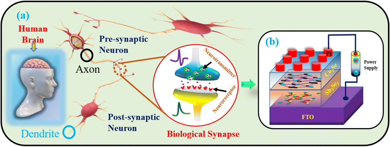 | ||
| Fig. 1 (a) The human biological neural system consists of pre-synaptic neurons and post-synaptic neurons interconnected through synapses, as clearly depicted in the magnified image. (b) The schematic of the electronic multilayer synapse structure (Pt/Cu2Se/Sb2Se3/FTO) that works like a human biological synapse. | ||
Fig. 2(a) presents the energy dispersive X-ray spectroscopy (EDS) data, which confirms the elemental composition of Cu, Sb and Se. Fig. 2(b) is the cross-sectional scanning electron microscopic (SEM) image, demonstrating the multilayer deposition of the Cu2Se and Sb2Se3 thin films on the FTO substrate. The distinct layers in the thin film device could be distinguished clearly, as shown in the inset of Fig. 2(b); however, the possible interdiffusion of layers across the interface cannot be ruled out. Fig. 2(c) shows the SEM images of the synthesised thin film, and the calculated average grain size of the deposited thin film was ∼250 nm (±20 nm). It was observed that the thin film was deposited uniformly and homogeneously on the FTO substrate, as shown in the inset of Fig. 2(c). The atomic force microscopy (AFM) analysis (Fig. 2(d)) confirmed that the calculated root means square surface roughness of the thermally deposited thin film structure was 8 nm.
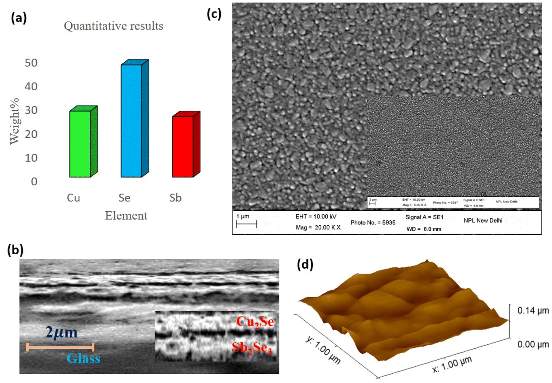 | ||
| Fig. 2 (a) The elemental composition of Cu2Se and Sb2Se3 by using EDS. (b) Cross-sectional SEM image of the multilayer structure of Cu2Se and Sb2Se3. In the inset, the magnified images of the Cu2Se and Sb2Se3 layers can be distinguished easily. (c) The top-view SEM image of the multilayer structure. The inset image shows that the film was deposited uniformly. (d) The AFM image used to calculate the surface roughness. | ||
To emulate the functionality of the biological synapse, low- and high-resistance states must be acquired. Therefore, the electrical measurement of the artificial synaptic device (Pt/Cu2Se/Sb2Se3/FTO) was carried out with a dual sweep of the DC voltage. We swept the voltage from −3.5 V to 0 V to 4.5 V; initially, the device remained in the low-resistance state (LRS), and the current was in the range of 10−2 A, as depicted in region (1) of Fig. 3(a). At low voltages, the resistance state of the device did not change, as depicted in region (2). When the DC voltage reached around 3 V, the current started to decrease gradually, and the corresponding voltage is referred to as the RESET voltage (VRESET), as depicted in region (3). Beyond 3 V, the resistance state completely transformed from the LRS to a high-resistance state (HRS) gradually. On the other hand, while decreasing voltage sweep, the cyclic current changed linearly in the I–V graph over a linear scale (not shown), which indicates ohmic behaviour between the device and contacts, as depicted in regions (2) and (4). Subsequently, the polarity of the applied voltage was changed and swept from 4.5 V to 0 V to −3.5 V; the HRS state did not change, as shown in regions 4 and 5, leading to memory formation in the form of resistance because it creates a memory window between the two states at the same voltage, as depicted in Fig. 3(a). Beyond −2 V, again the state of HRS gradually started to switch to the LRS corresponding to the SET voltage (VSET), which is the significance of analog bipolar resistive switching. It is evident that the device exhibits bipolar resistive switching behaviour. The reproducibility of the device during SET and RESET operations was also observed and showed utmost identical behaviour to other similar devices. The device VSET (HRS to LRS) exhibited good consistency for switching resistance; however, VRESET (LRS to HRS) spans a voltage window within acceptable limits, and it may be the result of improper formation of some conducting filaments during VSET, and they ruptured in the early stage of positive voltage sweep as shown in the ESI (S1†). We measured the bipolar resistive switching in various other devices that show the same utmost behaviour.
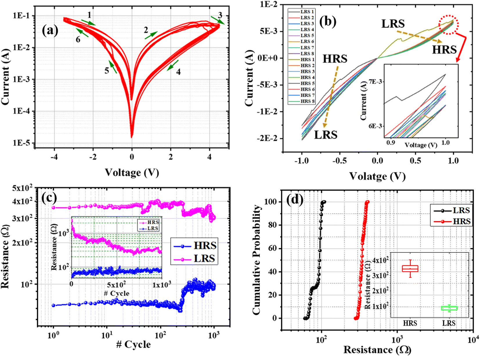 | ||
| Fig. 3 Electrical characteristics: (a) the I–V characteristics of the Pt/Cu2Se/Sb2Se3/FTO device, indicating analog behaviour during the continuous cycles of SET and RESET. (b) The gradual increase and decrease in conductance with the application of repeated fixed voltage sweeps to SET and RESET the device. In the inset, a magnified area under the red circle shows the change in conductance during RESET. (c) The endurance test of the Pt/Cu2Se/Sb2Se3/FTO device was conducted under DC conditions. The inset shows the initial 103 pulse cycle, indicating that the device reached stability after 600 cycle. The inset of figure (c) presents the stability of the HRS and LRS states of the device when the cycles were further extended by up to 103 cycle under the same conditions. (d) The probability distribution of HRS and LRS evidences that the LRS state is more stable after 600 cycle, but HRS fluctuates. In the inset, the error bar chart is used to check the dispersion of the LRS and HRS states. | ||
The conductance of the analog device increased (decreased) gradually whenever it switched from HRS to LRS and LRS to HRS under consecutive repeated voltage sweep cycles of 0 V to −1 V and 0 V to 1 V, as depicted in Fig. 3(b). These results influence the transition of short-term memory to long-term memory. The inset of Fig. 3(b) shows a magnified area covered under the red circle, which indicates that the conductance decreased gradually, approaching the long-term forgetting memory. However, to test for its analog resistive switching and possible application as a neural network, we checked the conductance of the devices at very low applied voltages far below the voltage of any type of sharp resistive switching. Gradually increased (decreased) of the conductance in the resistive switching device is analogous to the respective synaptic potentiation and depression behaviours.
To test the DC endurance of the Pt/Cu2Se/Sb2Se3/FTO device, we applied 103 write-and-read pulse cycles. The device was switched from HRS to LRS using a −3.5 V write pulse with a pulse width of 100 ms and from LRS to HRS using a 4.5 V write pulse with a pulse width of 100 ms. In both cases, a 0.2 V read pulse with a 100 ms pulse width was used to read the data. The HRS state showed degradation up to 600 cycles, as shown in the inset of Fig. 3(c). The instability at the starting phase of endurance measurements may have occurred due to the breakdown of some weakly formed conductive filament of selenium vacancies (VSe). To illustrate the stability concern in both the resistance states, we extended the cycles further by 103 pulse cycles, and both states (HRS and LRS) remained stable in comparison with the measured states of the preceding 103 pulse cycles, as illustrated in Fig. 3(c). In addition, it could be seen that the resistance OFF/ON ratio between HRS and LRS was ≈4. The obtained ratio is small, but the device is performing the switching process necessary for neuromorphic computing, which may help in the coming decades. For validation, we checked the endurance cycles in other devices and found similar behaviour, as shown in ESI (S2†). The graph in Fig. 3(d) was plotted to check the cumulative probability distribution of the LRS and HRS resistance values, of which HRS exhibited scattering to a certain extent, but the LRS state was comparatively less scattered; and this can be appropriate for memory applications if further research can be done. Hypothetically, we can say that this behaviour may be due to the improper formation of conducting filaments inside both of the multilayer cells. The statistics of the inset in Fig. 3(d) show less dispersive LRS values plotted in the error bar chart. A new device must initially undergo some stabilisation cycles before it can be used in new applications. Nevertheless, these results may be acceptable for valuable outcomes in future studies.
For high-density data storage, there is one possible way for the realization of multi-bit data storage in RRAM. It was carried out by controlling the intermediate resistance states by varying the SET and RESET voltages. Initially, the device under test (DUT) was brought to HRS with a high-amplitude positive voltage sweep. In fact, the multi-resistance state of the device was switched from HRS to LRS using a series of consecutive voltage sweep cycles, including 0 V to −2 V, −2.25 V, −2.5 V, −3 V, and −3.25 V, and the different current levels were observed. Similarly, to switch from LRS to HRS, we performed a series of consecutive voltage sweep cycles, including 0 V to 4 V, 5 V, 5.5 V, 5.75 V, 6.25 V and 6.5 V, and the varied current levels were obtained. The different current levels after every cycle in the negative and positive sweep cycles in Fig. 4(a) confirm multilevel switching in the same device.
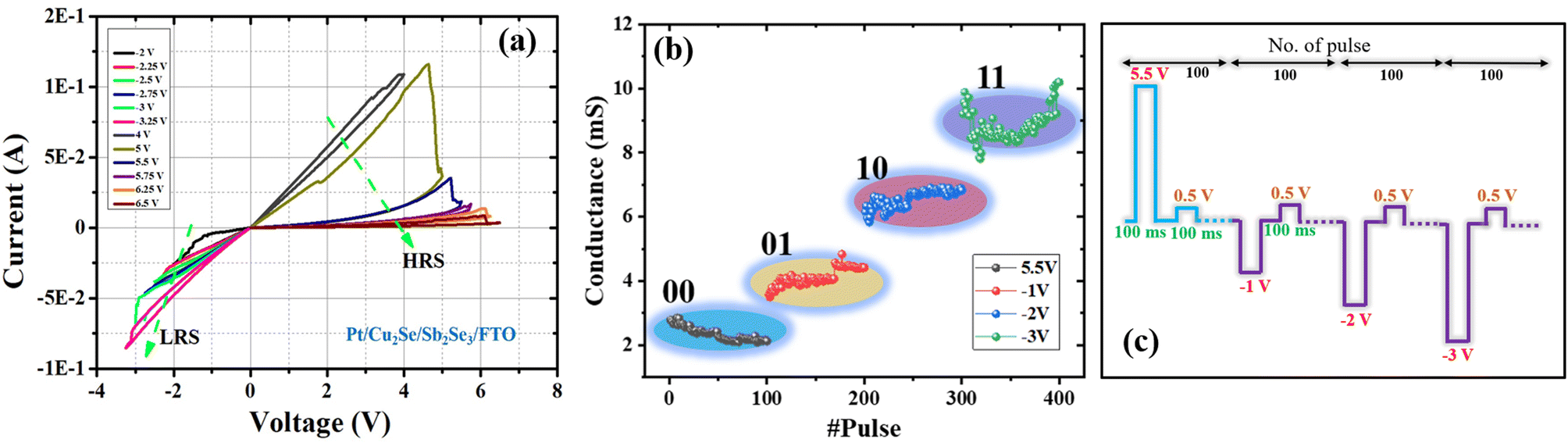 | ||
| Fig. 4 (a) The endurance of the multilevel switching characteristics of the Pt/Cu2Se/Sb2Se3/FTO device during SET operation. (b) The possible combinations of the multi-bit resistance states (00, 01, 10, and 11) and each resistance state measured for 100 pulse cycles. A total of 400 pulse cycle were run to achieve multiple states. (c) The applied pulse patterns to achieve multilevel switching of the device. | ||
The possible combinations of the multi-bit resistance states, which can be considered as 00, 01, 10, and 11 for data writing and erasing, were measured in the Pt/Cu2Se/Sb2Se3/FTO device. Fig. 4(b) clearly describes the multiple states that are reached during bipolar resistive switching. To achieve these multi-states of 00, 01, 10, and 11, we ran 400 exciton pulse cycles (100 pulse cycles for individual states). Initially, the device had to be RESET to the 00 state by applying 5.5 V and the 01, 10, and 11 states by applying −1 V, −2 V and −3 V, respectively. The data of these multi-states were read at 0.5 V after an interval time of 100 ms between the write and read pulses, as shown in the pulse pattern (Fig. 4(c)). For high-density memory storage, multi-states are essential aspects of synaptic devices. The conductance of the distinct resistive states could be achieved by controlling the stop voltage during the SET and RESET processes. These multi-resistance states occurred without any set compliance current. They could be modulated only by varying the pulse amplitude, suggesting that Pt/Cu2Se/Sb2Se3/FTO is a non-compliance-worthy artificial synaptic structure for neuromorphic computing applications. Therefore, this can be a potential multilevel storage memory device for next-generation neuromorphic computing systems.
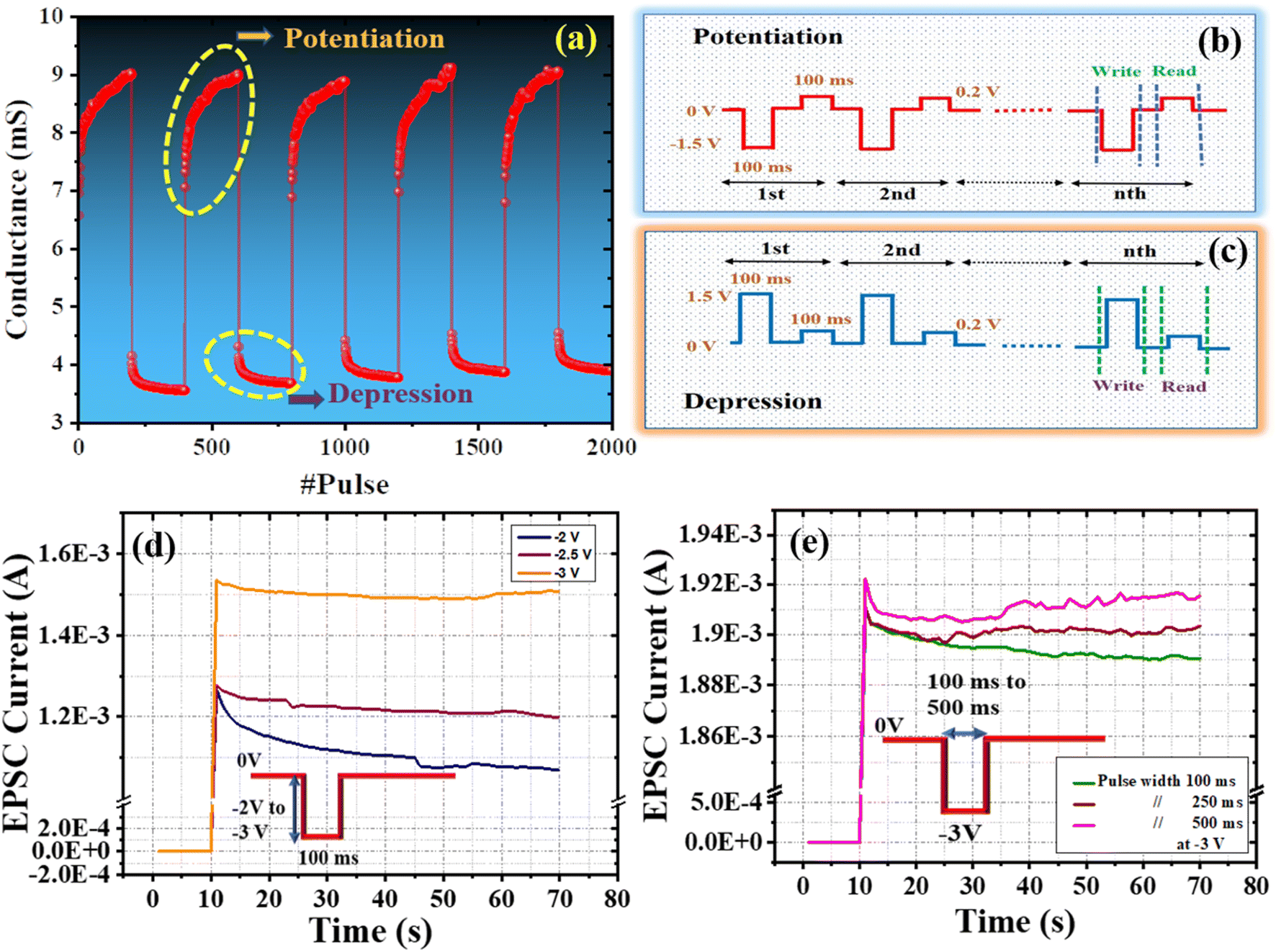
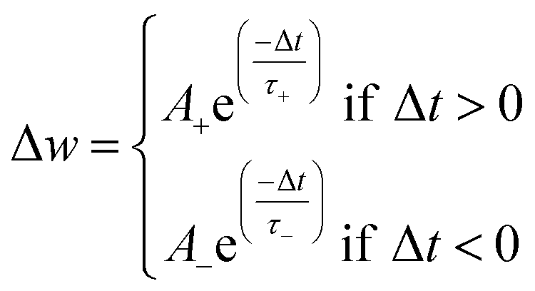
To mimic the complex biological neural function of the human brain, the device must emulate the variations in synaptic weight, which is the most important factor in a synaptic device.5 Besides the voltage sweep, we emulated the long-term potentiation (LTP) and long-term depression (LTD) characteristics of human biological synapses. Here, we investigated the neuromorphic characteristics of the Pt/Cu2Se/Sb2Se3/FTO artificial synaptic device in terms of LTP and LTD. Initially, the device was in the RESET state, but after applying the constant voltage write-pulse train of −1.5 V with a pulse width of 100 ms for potentiation and 1.5 V with a pulse width of 100 ms for depression, the conductance of the device changed gradually, as shown in Fig. 5(a). The conductance of the device was measured up to 200 cycles each for potentiation and depression. The conductance of the device was measured by applying a 0.2 V read pulse after every write pulse. The pulse delay between the write and read pulses was 100 ms. The applied pulse pattern, including the pulse amplitude and pulse width of the write and read pulses to get the potentiation and depression curve, is well illustrated in Fig. 5(b) and (c). The relationship of conductance versus the number of pulse cycles was consistent for 2000 pulse cycles. In response to the pulse train, the measured LTP and LTD were similar to the LTP and LTD of a human biological synapse. LTP and LTD usually occur after the rehearsal of short-term potentiation and short-term depression; this process is known as learning, which is fundamental for the adaptation of living beings.32 The term learning is related to the fact that if something is continuously learned over a long period, the probability of remembering would be higher, which clears the transition of short-term to long-term memory. Here, short-term stands for fast forgetting rates (fast decay of conductance) of the memory for the first few cycles, as we can see in the conductance curve. Besides, according to the Hebbian learning rule, synapses enhance post-neuron excitability, but excessive excitability is not required, meaning the synaptic weight of potentiation must be saturated.33 In the proposed device, the conductance approaches the saturation level after the rehearsal of some applied pulses. This excitation phenomenon is related to long learning memory.34 The gradual increase and decrease of LTP and LTD can be used for neuromorphic computing applications.35
 | ||
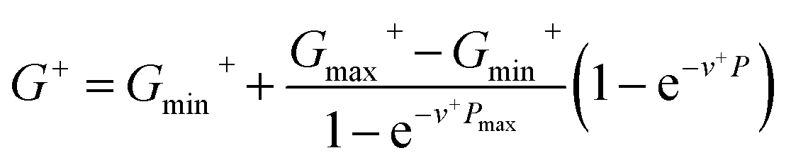
| Fig. 5 (a) The potentiation and depression characteristics of the Pt/Cu2Se/Sb2Se3/FTO device. (b) The applied 200 SET train pulses (−1.5 V, 100 ms) demonstrate potentiation. (c) The applied 200 RESET train pulses (1.5 V, 100 ms) demonstrate depression characteristics. A total of 2000 pulse cycles were applied to demonstrate the reproducibility of potentiation and depression. (d) EPSC decay after the application of a single short pulse with varying pulse amplitudes (−2 V, −2.5 V and −3 V) and a fixed 100 ms pulse width. Inset image: the pattern of pulses with different amplitudes and a fixed pulse width. (e) The EPSC decay rate after the application of variable pulse widths (100 ms, 250 ms and 500 ms) and a fixed −3 V pulse amplitude. Inset image: the pattern of pulses with different pulse widths and a fixed pulse amplitude. | ||
When an action potential strikes the axon, neurotransmitters are released from the pre-synaptic neuron to the post-synaptic neuron, due to which the signal is transmitted between two neurons via a synapse, as discussed in Fig. 1(a). In neuroscience terms, the generated action potential is transmitted from the pre- to post-synaptic neuron via a synapse, likely producing an excitatory post-synaptic current (EPSC) that likely triggers a post-synaptic neuron to generate an action current.36,37 Short-term plasticity, which is considered the physiological basis of the necessary computation, illustrates that the synaptic response rapidly degrades on a time scale of a few seconds, while long-term plasticity response, which imparts the capacity for learning and memory, often lasts for minutes to hours.38 In the proposed multilayer device, the top and bottom metal electrodes work like the pre-synaptic and post-synaptic neurons in the biological neural system.39 Fig. 5(d) illustrates the EPSC characteristics when a single short voltage pulse of different amplitudes was applied (−2 V, −2.5 V, and −3 V). Initially, a −2 V/100 ms write pulse was applied, as depicted in the inset of Fig. 5(d); the EPSC current increased sharply and then decayed gradually, showing an exponential trend over 60 seconds from its peak value, which is essentially the synaptic dynamic function. The EPSC current data were read continuously by applying a read pulse of 0.2 V with a 100 ms pulse width. These read pulses were applied after every 1 second. At −2.5 V and −3 V, the EPSC current amplitudes were higher than the previous ones, and the decay rate for a few seconds was low compared with the previous EPSC current level, leading to long-term plasticity. For memory consolidation, the transition of short-term plasticity to long-term plasticity could be realized by increasing the pulse amplitude, as depicted in Fig. 5(d), which shows higher amplitudes lead to stronger synaptic weight modulation. In induced EPSC, pulse sharpness from the pre-synaptic neuron also plays an essential role in transferring the electrical signal from the pre-synaptic neuron to the post-synaptic neuron. Furthermore, the amplitude of −3 V was fixed and varying pulse widths (100 ms, 250 ms, and 500 ms) were employed to study the effect on the current and decay rate of the synaptic device. Among these different applied pulses, the device behaved like a human brain in terms of the transition of short-term plasticity to long-term plasticity at the 100 ms pulse width. Whereas, at broader pulse signals, it did not show proper biological activities. The pattern of the applied pulse sharpness is shown in the inset of Fig. 5(e).
To train the neural network, the Hebbian learning rule (HLR) is fundamental and is very important to validate the execution of artificial synaptic devices. To implement the HLR, we must demonstrate STDP.2,40,41 STDP is the essential characteristic of synaptic plasticity and is associated with two different stimuli signals in the presence of time. On the other hand, the weight of an artificial synaptic device in STDP can be altered by pre-and post-synaptic stimulation.3
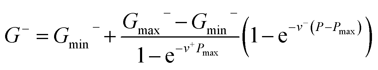
In order to emulate the STDP rule, a pulse pair signal with a pre-synaptic and post-synaptic spike amplitude of V−/V+ = −3 V/4 V was implemented to the top and bottom electrodes, respectively. The applied pre-and post-synaptic pulse designs are shown in (I) and (III) quadrants of Fig. 6. It can be seen that when the relative time difference decreased, more significant synaptic weight changes would occur in both cases (Δt > 0 and Δt < 0). Here, Δt (Δt = tpost-spike − tpre-spike) is the relative time difference, which defines the time interval between the end spike of a pre-synaptic neuron and the initial spike of the post-synaptic neuron, as illustrated in (I) and (III) quadrants of Fig. 6. Between the pre-and post-synaptic spike pairs, an interval of 5 seconds is long enough to ignore the effect of V− and V+ according to the decay time of EPSC.3,42 For STDP, the percentage synaptic weight change (Δw%) for Δt was calculated by using the equation Δw% = ((Gafter − Gbefore)/Gbefore) × 100, where Gafter and Gbefore are the conductance values after the current stimulation and previous stimulation, respectively. When the pre-synaptic spike pairs reach before the post-synaptic spike pairs, Δw enhanced with decreasing Δt. On the contrary, when the post-synaptic spike pairs reach before the pre-synaptic spike pairs, Δw decreased along with an increase in Δt. In the (II) quadrant, when Δt < 0, a positive synaptic weight change occurs, which indicates synaptic potentiation, and in the (IV) quadrant, when Δt > 0, a negative synaptic weight change occurs, which indicates device depression. The relationship between the relative change in synaptic weight and the spike time difference is consistent with the STDP biological synapse. For the STDP learning rule, Δw is established by defining the function of exponential fitting.43,44
 | (1) |
 | ||
| Fig. 6 In quadrants (II) and (IV), the synaptic weight change (Δw%) STDP is presented as a function of the relative time change (Δt) between the pre-and post-synaptic paired pulse propagation. In quadrants (I) and (III), schematic representations of the pre-synaptic and post-synaptic applied paired pulses are given. | ||
Additionally, the handwritten numerical digit pattern recognition accuracy of the device was tested using MNIST. The corresponding LTP/LTD data of the Pt/Cu2Se/Sb2Se3/FTO device were plotted as normalized conductance values, as shown in Fig. 7(a) and (b). The obtained normalized conductance dataset was fitted to the following equations.45
 | (2) |
 | (3) |
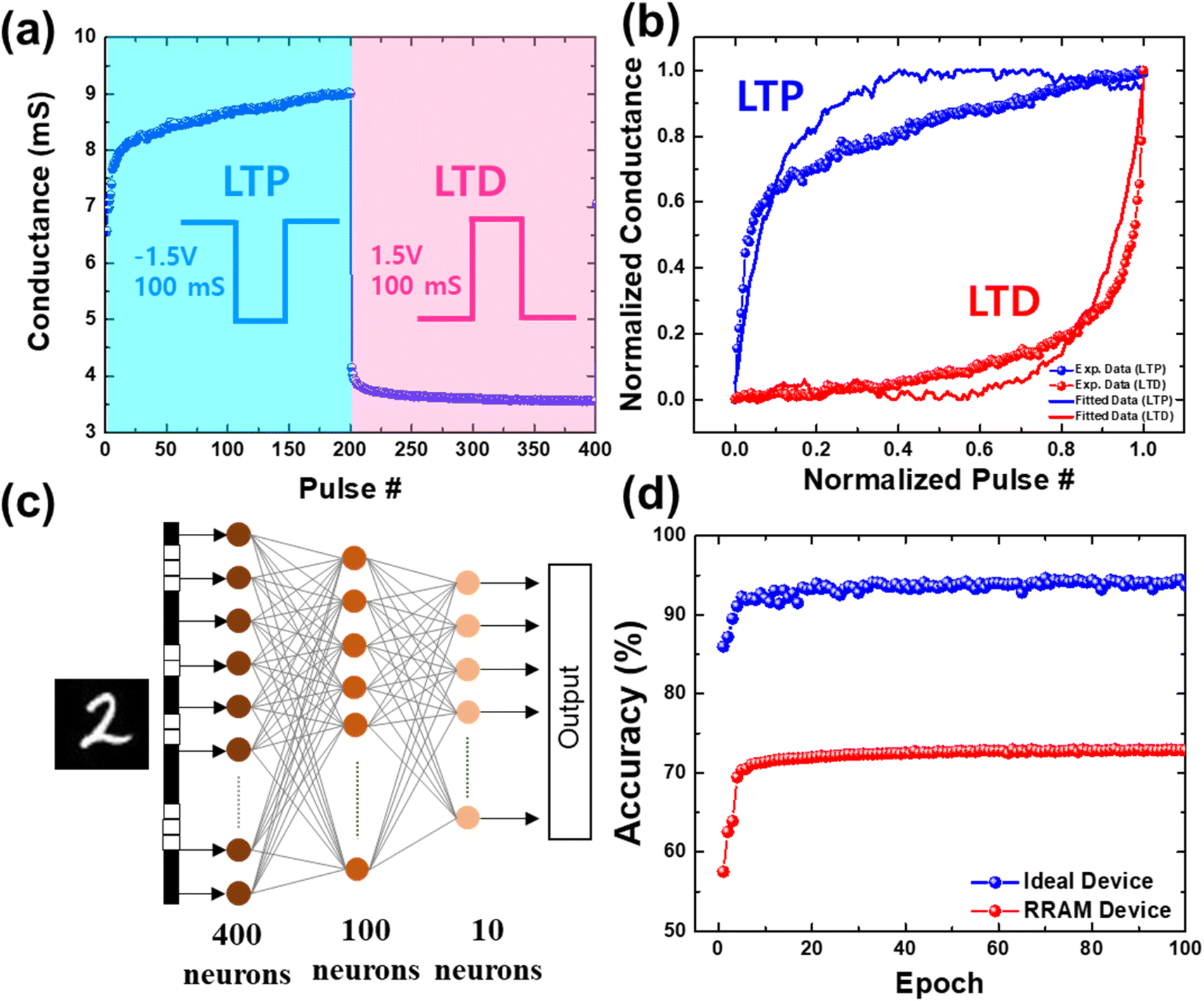 | ||
| Fig. 7 The MNIST pattern recognition simulation of the Pt/Cu2Se/Sb2Se3/FTO devices. (a) The conductance plot was obtained in the LTP and LTD operations. (b) The calculated normalized conductance of the devices with curve fitting. (c) The depiction of the employed synapse neural network comprising an input layer of 400 neurons, a hidden layer of 100 neurons and an output layer of 10 neurons for MNIST pattern recognition. (d) The simulated accuracy curves of the ideal and Pt/Cu2Se/Sb2Se3/FTO devices on the MNIST dataset. | ||
The synapse neural network architecture employed for the simulation has been depicted in Fig. 7(c). The simulation of image classification was performed using the MNIST dataset consisting of a database of handwritten digits with ten classes. The accuracy plots of the ideal device and the Pt/Cu2Se/Sb2Se3/FTO device were plotted for the comparison, as shown in Fig. 7(d). The calculated accuracy plot over 100 epochs indicated that the Pt/Cu2Se/Sb2Se3/FTO device exhibited a max accuracy of ∼73%, which is slightly lower than that of the ideal RRAM device (∼94.5%). Due to the increased nonlinearity (∼6.54), the accuracy of the Pt/Cu2Se/Sb2Se3/FTO devices appears significantly lower than that of the ideal device. However, the accuracy plot saturated nearly 15 epochs.
An extensive comparison of many chalcogenide materials is presented in Table 1. In order to assess the performance of the proposed RRAM device, the resistive switching phenomenon has been viewed in a variety of ways. However, each of the materials listed below has a distinct behaviour. In the Pt/Cu2Se/Sb2Se3/FTO device, VSET and VRESET are a little bit higher compared to other cited materials, but it shows interesting characteristics such as multilevel switching and high endurance. The calculated MNIST pattern shows slightly lower accuracy than Ag–Ge30Se70 and may increase upon exploring more possibilities through research. Sb2Se3 is sensitive to optical illumination, which is advantageous for the optical tunability aspect of synaptic plasticity. There has been a great deal of research into these materials. The accuracy can be enhanced if more research is done in the future.
| S. no | Materials | VSET (V) | VRESET (V) | Endurance cycles | Switching | Multilevel | MNIST pattern | Ref. |
|---|---|---|---|---|---|---|---|---|
| 1 | Ag/Sb2Se3/W | 5 | −5 | — | Analog | No | No | 46 |
| 2 | ReSe2/graphene | 3.5 | −4 | 250 | Digital | No | No | 47 |
| 3 | SnSe/SrTiO3 | 2.5 | −0.6 | — | Digital | Yes | No | 48 |
| 3 | Al/Cu2Se/Pt | 0.4 | −0.3 | — | Analog | No | No | 49 |
| 4 | Ag/Sb2Te3/Ag | −1 | 1 | 102 | Analog | Yes | No | 50 |
| 6 | Au/MoS2/Au | ≈2.9 | ≈−2 | — | Analog | Yes | No | 51 |
| 7 | TiN/GeSbTe/TiN | — | — | 70 | Analog | Yes | No | 52 |
| 8 | Ag–Ge30Se70 | ≈0.15 | ≈−0.1 | — | Analog | Yes | 79%, 87% | 53 |
| 9 | Pt/Cu2Se/Sb2Se3/FTO | −3.5 | 4.5 | 103 | Analog | Yes | 73% | This device |
The possible fundamental mechanism of resistive switching in the as-prepared device is proposed. It may involve the migration of ions and vacancies inside the Pt/Cu2Se/Sb2Se3/FTO thin film structure. In the absence of an external power supply, there is no movement of ions and vacancies, as shown in Fig. 8(a). When a negative voltage is applied to the top electrode (Pt) and a positive terminal is connected to the bottom electrode (FTO), VSe is formed54,55 and moves towards the top electrode, whereas Se2− starts moving towards the bottom electrode in both cells, as shown in Fig. 8(b). These VSe form thin conducting filaments through which floods of electrons move from Pt to the FTO electrode, causing the device to switch from the HRS state to the LRS state, as illustrated in Fig. 8(b). Conversely, when the polarity of the top and bottom electrodes is reversed, the conducting filaments are destroyed due to the recombination of VSe and Se2− ions in the upper and lower electrolyte cells, as demonstrated in Fig. 8(c). This causes the device to switch back from LRS to HRS. Therefore, the primary mechanisms behind the Pt/Cu2Se/Sb2Se3/FTO synaptic devices are based on Se2− ionic movement, VSe, filament formation and destruction.
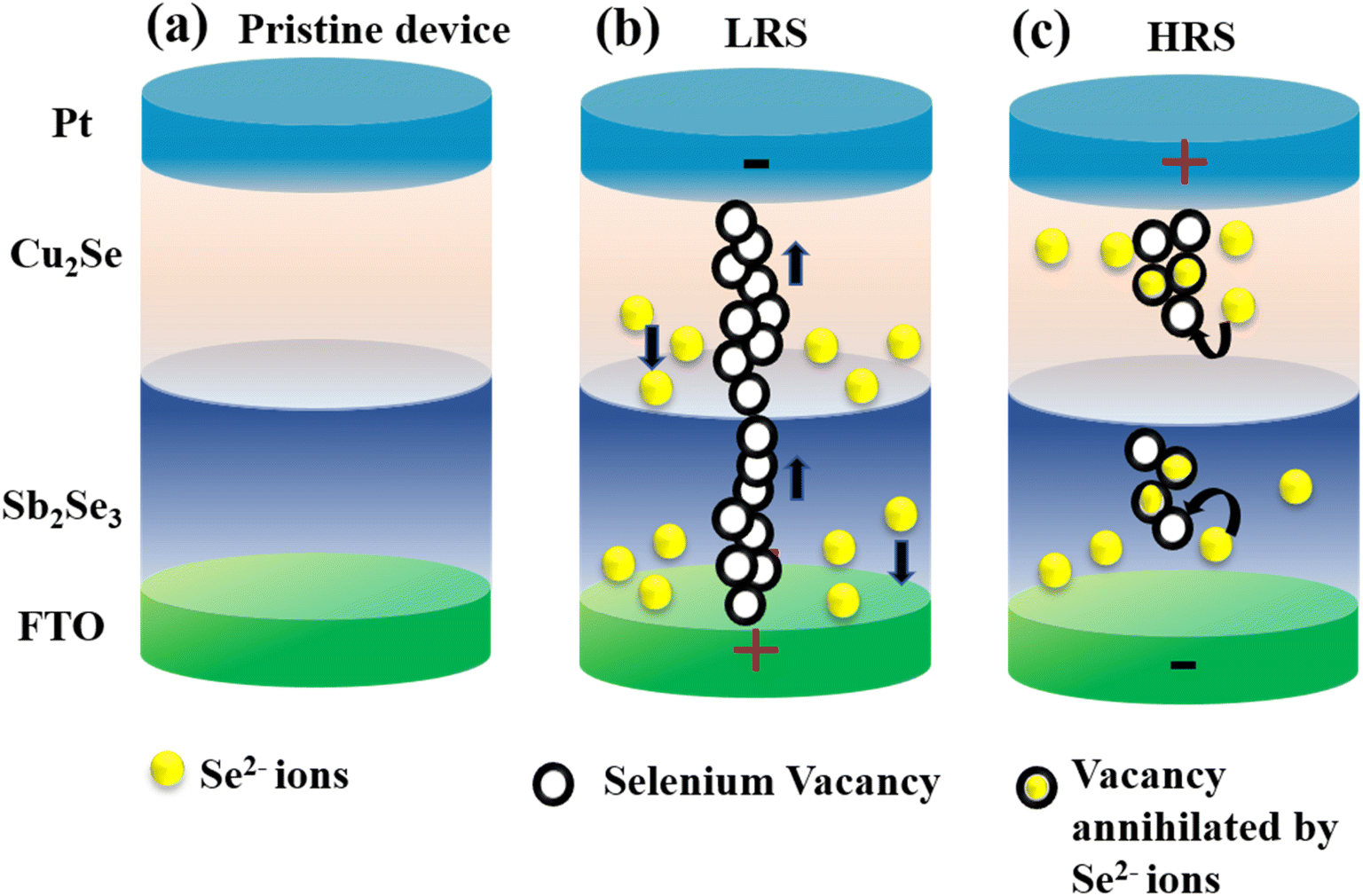 | ||
| Fig. 8 A schematic representation of the internal mechanism: (a) in the absence of an external power supply, no movement of ions and vacancies happens. (b) When the negative and positive terminals are connected respectively to the top and bottom electrodes, the migration of VSe and Se2− starts in the upper cell (Cu2Se) and lower cell (Sb2Se3). The migration of VSe forms the conducting filament during SET operation in both cells. (c) When the negative and positive terminals are connected respectively to the bottom and top electrodes, VSe recombines with Se2− ions in both cells during RESET operation. | ||
4. Conclusions
A memristive device with a multilayer Pt/Cu2Se/Sb2Se3/FTO structure was fabricated by thermal evaporation and the DC sputtering technique. This device illustrated that resistance modulation behaves like analog bipolar resistive switching. It exhibited various synaptic functions that emulate the human biological neural system. The device resistance switched from HRS to LRS and LRS to HRS over 103 repetitive pulse cycles during the endurance test. The device demonstrated stable endurance in the two resistance states with a resistance ratio of 4 after extending the first 103 pulse cycles. By using repetitive pulse cycles, it was successfully possible to produce the crucial functions of a synapse, which include a nonlinear change in conductance, multilevel switching, potentiation/depression, and the transition of short-term memory to long-term memory. EPSC and STDP have also been demonstrated in the device to implement HLR for futuristic neuromorphic computing applications. The proposed Pt/Cu2Se/Sb2Se3/FTO device showed a simulated MNIST pattern recognition accuracy of about 73%, indicating considerable potential in memristor-based neuromorphic systems. These findings might be useful for neuromorphic computing.Author contributions
M. Asif and Ashok Kumar conceived the problems and performed the experiment, wrote the manuscript and analysed the data. Atul Thakre supported the manuscript writing and analysed the data. Yogesh Singh and V. N. Singh fabricated the device and support the manuscript writing and analysed the data.Conflicts of interest
There are no conflicts to declare.Acknowledgements
The authors are grateful to the Director, CSIR-NPL, and the head of the Physico-Mechanical Metrology Division, for pro facilitating infrastructure and laboratory facilities, CSIR-NPL, India. The authors also want to thank Dr Ved Varun Agrawal and Dr J. S. Tawale for their experimental support. The author, Mr Mohd Asif, would also like to acknowledge AcSIR for allowing him to pursue PhD.References
- Q. Wan, M. T. Sharbati, J. R. Erickson, Y. Du and F. Xiong, Adv. Mater. Technol., 2019, 4, 1900037 CrossRef.
- S. Sagar, K. Udaya Mohanan, S. Cho, L. A. Majewski and B. C. Das, Sci. Rep., 2022, 12, 3808 CrossRef CAS PubMed.
- L. G. Wang, W. Zhang, Y. Chen, Y. Q. Cao, A. D. Li and D. Wu, Nanoscale Res. Lett., 2017, 12, 1–8 CrossRef PubMed.
- J. Park, H. Ryu and S. Kim, Sci. Rep., 2021, 11, 1–7 CrossRef PubMed.
- Y. Kim, C. H. Park, J. S. An, S. H. Choi and T. W. Kim, Sci. Rep., 2021, 11, 1–10 CrossRef PubMed.
- R. Khan, N. Ilyas, M. M. Zubair Shamim, M. Ilyas Khan, M. Sohail, N. Rahman, A. Ali Khan, S. Naz Khan and A. Khan gh, J. Mater. Chem. C, 2021, 9, 2012–2016 Search PubMed.
- P. S. Ioannou, E. Kyriakides, O. Schneegans and J. Giapintzakis, Sci. Rep., 2020, 10, 1–10 CrossRef PubMed.
- J. H. Ryu, C. Mahata and S. Kim, J. Alloys Compd., 2021, 850, 156675 CrossRef CAS.
- S. Hao, X. Ji, S. Zhong, K. Y. Pang, K. G. Lim, T. C. Chong and R. Zhao, Adv. Electron. Mater., 2020, 6, 1901335 CrossRef CAS.
- Y. Wang, Z. Lv, L. Zhou, X. Chen, J. Chen, Y. Zhou, V. A. L. Roy and S. T. Han, J. Mater. Chem. C, 2018, 6, 1600–1617 RSC.
- M. Asif and A. Kumar, J. Alloys Compd., 2021, 859, 158373 CrossRef CAS.
- J. Li, Q. Duan, T. Zhang, M. Yin, X. Sun, Y. Cai, L. Li, Y. Yang and R. Huang, RSC Adv., 2017, 7, 43132–43140 RSC.
- M. K. Hota, M. N. Hedhili, Q. Wang, V. A. Melnikov, O. F. Mohammed and H. N. Alshareef, Adv. Electron. Mater., 2015, 1, 1400035 CrossRef.
- N. Raeis-Hosseini, S. Chen, C. Papavassiliou and I. Valov, RSC Adv., 2022, 12, 14235–14245 RSC.
- T. Huang, R. Zhang, L. Zhang, P. Xu, Y. Shao, W. Yang, Z. Chen, X. Chen and N. Dai, RSC Adv., 2022, 12, 35579–35586 RSC.
- Y. Huang, J. Yu, Y. Kong and X. Wang, RSC Adv., 2022, 12, 33634–33640 RSC.
- M. Asif and A. Kumar, Materials Today Electronics, 2022, 1, 100004 CrossRef.
- Y. Yuan, X. Cao, Y. Sun, J. Su, C. Liu, L. Cheng, L. Yuan, H. Zhang and J. Li, RSC Adv., 2017, 7, 46431–46435 RSC.
- Y. Yuan and J. Li, Electron. Lett., 2018, 54, 169–171 CrossRef CAS.
- M. Malligavathy, R. T. Ananth Kumar, C. Das, S. Asokan and D. Pathinettam Padiyan, J. Non-Cryst. Solids, 2015, 429, 93–97 CrossRef CAS.
- W. Kim, C. Yoo, E. S. Park, M. Ha, J. W. Jeon, G. S. Kim, K. S. Woo, Y. K. Lee and C. S. Hwang, ACS Appl. Mater. Interfaces, 2019, 11, 38910–38920 CrossRef CAS PubMed.
- S. Rehman, K. Kim, J. H. Hur and D. K. Kim, J. Phys. D: Appl. Phys., 2017, 50, 135301 CrossRef.
- A. Basak and U. P. Singh, Sol. Energy Mater. Sol. Cells, 2021, 230, 111184 CrossRef CAS.
- J. Henry, T. Daniel, V. Balasubramanian, K. Mohanraj and G. Sivakumar, Inorg. Nano-Met. Chem., 2021, 51, 38–46 CrossRef CAS.
- F. M. Kiessling, P. Rudolph and F. M. Kiessling, Cryst. Res. Technol., 1988, 23, 1207–1224 CrossRef.
- Y. Singh, M. Kumar, R. Yadav, A. Kumar, S. Rani, Shashi, P. Singh, S. Husale and V. N. Singh, Sol. Energy Mater. Sol. Cells, 2022, 243, 111765 CrossRef CAS.
- X. Yan, Z. Zhou, B. Ding, J. Zhao and Y. Zhang, J. Mater. Chem. C, 2017, 5, 2259–2267 RSC.
- D. Kumar, S. Shrivastava, A. Saleem, A. Singh, H. Lee, Y.-H. Wang and T.-Y. Tseng, ACS Appl. Electron. Mater., 2022, 4, 2180–2190 CrossRef CAS.
- S. R. Zhang, L. Zhou, J. Y. Mao, Y. Ren, J. Q. Yang, G. H. Yang, X. Zhu, S. T. Han, V. A. L. Roy and Y. Zhou, Adv. Mater. Technol., 2019, 4, 1800342 CrossRef.
- W. Wang, G. Pedretti, V. Milo, R. Carboni, A. Calderoni, N. Ramaswamy, A. S. Spinelli and D. Ielmini, Sci. Adv., 2018, 4, 4752–4764 CrossRef PubMed.
- J. del Valle, J. G. Ramírez, M. J. Rozenberg and I. K. Schuller, J. Appl. Phys., 2018, 124, 211101 CrossRef.
- M. Pereira, J. Deuermeier, R. Nogueira, P. A. Carvalho, R. Martins, E. Fortunato and A. Kiazadeh, Adv. Electron. Mater., 2020, 6, 2000242 CrossRef CAS.
- X. Zhang, S. Liu, X. Zhao, F. Wu, Q. Wu, W. Wang, R. Cao, Y. Fang, H. Lv, S. Long, Q. Liu and M. Liu, IEEE Electron Device Lett., 2017, 38, 1208–1211 CAS.
- S. Deswal, A. Kumar and A. Kumar, AIP Adv., 2019, 9, 095022 CrossRef.
- E. Yoo, M. Lyu, J. H. Yun, C. Kang, Y. Choi and L. Wang, J. Mater. Chem. C, 2016, 4, 7824–7830 RSC.
- S. Wang, C. He, J. Tang, R. Yang, D. Shi and G. Zhang, Chin. Phys. B, 2019, 28, 017304 CrossRef CAS.
- X. Yan, Z. Zhou, B. Ding, J. Zhao and Y. Zhang, J. Mater. Chem. C, 2017, 5, 2259–2267 RSC.
- J. Gao, X. Lian, Z. Chen, S. Shi, E. Li, Y. Wang, T. Jin, H. Chen, L. Liu, J. Chen, Y. Zhu and W. Chen, Adv. Funct. Mater., 2022, 32, 2110415 CrossRef CAS.
- Z. Shen, C. Zhao, Y. Qi, W. Xu, Y. Liu, I. Mitrovic, L. Yang and C. Zhao, Nanomaterials, 2020, 10(8), 1437 CrossRef CAS PubMed.
- F. Zeng, S. Li, J. Yang, F. Pan and D. Guo, RSC Adv., 2014, 4, 14822–14828 RSC.
- X. Yang, C. Wang, J. Shang, C. Zhang, H. Tan, X. Yi, L. Pan, W. Zhang, F. Fan, Y. Liu, Y. Chen, G. Liu and R. W. Li, RSC Adv., 2016, 6, 25179–25184 RSC.
- Z. Q. Wang, H. Y. Xu, X. H. Li, H. Yu, Y. C. Liu and X. J. Zhu, Adv. Funct. Mater., 2012, 22, 2759–2765 CrossRef CAS.
- M. U. Khan, C. M. Furqan, J. Kim, S. A. Khan, Q. M. Saqib, M. Y. Chougale, R. A. Shaukat, M. H. Kang, N. P. Kobayashi, J. Bae and H. S. Kwok, ACS Appl. Electron. Mater., 2022, 4, 297–307 CrossRef CAS.
- C. Mahata, M. Kang and S. Kim, Nanomaterials, 2020, 10, 1–12 CrossRef PubMed.
- M. Kim, M. A. Rehman, D. Lee, Y. Wang, D. H. Lim, M. F. Khan, H. Choi, Q. Y. Shao, J. Suh, H. S. Lee and H. H. Park, ACS Appl. Mater. Interfaces, 2022, 14, 44561–44571 CrossRef CAS PubMed.
- C. Liu, Y. Yuan, L. Cheng, J. Su, X. Zhang, X. Li, H. Zhang, M. Xu and J. Li, Results Phys., 2019, 13, 102228 CrossRef.
- S. Rehman, H. Kim, M. F. Khan, J. H. Hur, J. Eom and D. kee Kim, J. Alloys Compd., 2021, 855, 157310 CrossRef CAS.
- T. L. Ho, K. Ding, N. Lyapunov, C. H. Suen, L. W. Wong, J. Zhao, M. Yang, X. Zhou and J. Y. Dai, Nanomaterials, 2022, 12, 2128 CrossRef CAS PubMed.
- S. Rehman, K. Kim, J. H. Hur and D. K. Kim, J. Phys. D: Appl. Phys., 2017, 50, 135301 CrossRef.
- X. Cao, C. Meng, J. Li, J. Wang, Y. Yuan, J. Su, C. Liu, X. Zhang, H. Zhang and J. Wang, Phys. Chem. Chem. Phys., 2018, 20, 18200–18206 RSC.
- S. Bhattacharjee, E. Caruso, N. McEvoy, C. Ó Coileáin, K. O'Neill, L. Ansari, G. S. Duesberg, R. Nagle, K. Cherkaoui, F. Gity and P. K. Hurley, ACS Appl. Mater. Interfaces, 2020, 12, 6022–6029 CrossRef CAS PubMed.
- A. H. Jaafar, L. Meng, Y. J. Noori, W. Zhang, Y. Han, R. Beanland, D. C. Smith, G. Reid, K. de Groot, R. Huang and P. N. Bartlett, J. Phys. Chem. C, 2021, 125, 26247–26255 CrossRef CAS.
- M. N. Kozicki, H. J. Barnaby, P. Apsangi, H. Barnaby, M. Kozicki, Y. Gonzalez-Velo and J. Taggart, Neuromorph. Comput. Eng., 2022, 2, 021002 CrossRef.
- M. A. Tumelero, R. Faccio and A. A. Pasa, J. Phys. Chem. C, 2016, 120, 1390–1399 CrossRef CAS.
- M. B. Costa, F. W. S. Lucas and L. H. Mascaro, ChemElectroChem, 2019, 6, 2937–2944 CrossRef CAS.
Footnote |
| † Electronic supplementary information (ESI) available. See DOI: https://doi.org/10.1039/d3ra02075d |
| This journal is © The Royal Society of Chemistry 2023 |