DOI:
10.1039/D3RA01492D
(Paper)
RSC Adv., 2023,
13, 14393-14411
Growth-control of hexagonal CdS-decorated ZnO nanorod arrays with low-temperature preheating treatment for improved properties and efficient photoelectrochemical applications
Received
6th March 2023
, Accepted 20th April 2023
First published on 11th May 2023
Abstract
The limitations of oxide semiconductor-based solar cells in achieving high energy conversion efficiencies have prompted incessant research efforts towards the creation of efficient heterostructures. Despite its toxicity, no other semiconducting material can fully replace CdS as a versatile visible light-absorbing sensitizer. Herein, we explore the aptness of preheating treatment in the successive ionic layer adsorption and reaction (SILAR) deposition technique and improve the understanding of the principle and the effects of a controlled growth environment on thus-formed CdS thin films. Single hexagonal phases of nanostructured cadmium sulfide (CdS)-sensitized zinc oxide nanorods arrays (ZnO NRs) have been developed without the support of any complexing agent. The influences of film thickness, cationic solution pH and post-thermal treatment temperature on the characteristics of binary photoelectrodes have been investigated experimentally. Interestingly, the preheating-assisted deposition of CdS, which is rarely applied for the SILAR technique, resulted in improved photoelectrochemical performance similar to the post-annealing effect. The X-ray diffraction pattern revealed that optimized ZnO/CdS thin films were polycrystalline with high crystallinity. Examination of the morphology of the fabricated films via field emission scanning electron microscopy showed that film thickness and medium pH altered the growth mechanism of nanoparticles, thereby changing their particle sizes, which had a significant influence on the film's optical behavior. The effectiveness of CdS as a photosensitizer and the band edge alignment for ZnO/CdS heterostructures were evaluated using ultra-violet visible spectroscopy. Facile electron transfer in the binary system as evidenced in electrochemical impedance spectroscopy Nyquist plots, therefore, promotes higher photoelectrochemical efficiencies from 0.40% to 4.30% under visible light illumination as compared with the pristine ZnO NRs photoanode.
1 Introduction
Photoelectrochemical (PEC), photocatalytic and photovoltaic technologies are known as the cleanest and most economical approaches to solar-driven renewable hydrogen production. Typically, the efficiency of photoinduced charge carrier separation can significantly alter the photocurrent conversion efficiency of participating semiconductor(s). For instance, fast electron–hole recombination rates in zinc oxide nanorod arrays (ZnO NRAs) limit the overall photoelectrochemical performance despite the one-dimensional nanostructured photoanode serving as an excellent electron transport pathway to improve electron collection for photocurrent generation.1 According to recently reported strategies, constructing a heterojunction is promising for maximizing the visible-light harvesting and subsequently, the electron–hole generation, separation and collection efficiency of a photoelectrode.2–4 In this context, different semiconductor band levels could result in type I (straddling gap), type II (staggered gap) or type III (broken gap) heterojunctions. In the type II heterojunction, electron–hole pairs can generally be separated more effectively than in type I and type III heterojunctions since the conduction and valence bands of two semiconductors are arranged step-wise so that the transfer of photogenerated electrons (between conduction bands of semiconductor A and B) and holes (between valence bands of semiconductor A and B) can simultaneously take place without accumulation on either semiconductor.4 Therefore, it suppresses electron–hole recombination and extends the charge carrier lifetime for preferred photo-response. Apart from that, the formation of a p–n heterojunction photoanode is also favourable for engineering the interface electronic properties and charge transfer mechanism. Liu and co-workers fabricated p-CuO/n-ZnO nanorod arrays that demonstrated 4-fold PEC enhancement contributed by broader visible-light absorption and better charge separation in the heterostructure.5 Sitara et al. coupled p-CoTe and n-MoS2 through sonochemical synthesis. The successful creation of the heterojunction was evidenced not only by a sharp decrement of the anodic onset potential but the effective interfacial interaction between each counterpart also reduced the charge transfer resistance.6
To fabricate a more functional ZnO-based nano-heterostructure, metal chalcogenides, especially CdX (where X = S, Se and Te), are dominant candidates due to their smaller bandgap energies, similar lattice with ZnO and suitable band alignment for the water splitting process. These features make it possible to harvest the full solar spectrum to achieve the desired solar-to-hydrogen (STH) conversion efficiency when coupled with wide bandgap semiconductors. The application of these visible II–VI semiconductors in quantum size facilitated the inter-band photo-injection of electrons from quantum dots (QDs) into the electron acceptor layer while the holes remained strongly confined in QDs, therefore significantly decreasing the surface traps and suppressing the exciton recombination.7 Synergistic effects of different Cd-based chalcogenides and ZnO nanostructures can be attained through surface sensitization or core–shell architecture. According to Mendhe and co-workers,8 a core–shell structure with a larger interface contact area is beneficial for the charge generation and tunnelling process. Besides this, the properties of the shell material can be tuned individually, for instance, by controlling the shell thickness, particle size and coverage, surface state passivation, etc., to boost the PEC performance. Due to an optical band gap of 1.45 eV and a light-harvesting capability of up to ∼860 nm, Consonni et al. fabricated ZnO/CdTe core–shell nanowire (NW) arrays in which the crystallinity was greatly improved with CdCl2 heat treatment and a short-circuit current density of 0.35 mA cm−2 was displayed.9 Before that, Yin et al.10 and Tak et al.11 developed CdSe and CdS-sensitized ZnO NWs, respectively. Different deposition conditions were manipulated until maximum photocurrent densities of 3.65 mA cm−2 and 3.32 mA cm−2 were observed, respectively. Fundamentally, CdS is considered to be more stable in polysulfide electrolyte and is less toxic if compared to CdSe and CdTe.12
As reported in most literature, the fabrication of the cascaded ZnO/CdS heterojunction is possible via the implementation of a simple successive ionic layer absorption and reaction (SILAR) method.7,8,11 Other than the advantageous charge transfer ability discussed above, the type-II heterostructure of ZnO/CdS is significant for inhibiting the photo-corrosion of CdS under light illumination, which is induced by the accumulation and oxidization of photogenerated holes.2 In this case, the crystal structure of heterojunction materials is an important consideration to avoid any lattice strain and especially to ensure the uniform distribution of the shell component.13 To the best of our knowledge, low-temperature chemical routes including the conventional SILAR process always produced cubic CdS or mixed phases of cubic and hexagonal CdS.14–16 Despite similar atom arrangements being found in both the cubic and hexagonal structures,17 different lattice constants could reveal different levels of lattice mismatch, which may lead to interfacial carrier recombination that causes optical loss and decays the PEC activity.18 The relatively thermodynamically stable hexagonal phase of CdS is, therefore, preferable for solar cell application.15,19
Herein, we have applied a two-step preheating treatment during the SILAR deposition process as one of the strategies to promote hexagonal CdS crystal formation and strengthen the heterojunction interface contact to enhance the PEC behaviour. Such low-temperature soft-bake treatment is common in the spin coating technique but it is rarely reported for the SILAR approach. However, it has been proved that a suitable two-step annealing treatment at low temperatures is significant for avoiding CdS film pinholes and excess element diffusion between heterojunction components that might be induced by direct high-temperature treatment; it also decreases the interfacial defect densities and crossover phenomenon within the kesterite-based solar cells.20,21 From the preliminary study, the ZnO/CdS heterojunction with two-step low-temperature preheating treatment showed an expected photocurrent density enhancement as compared to that of one-step or without any thermal treatment. Although there is a wealth of studies reported on the preparation of single or multi-component CdS nanostructures through the SILAR approach, a well-established discussion connected to the reaction mechanism change in different bath environments was seldom found. Since the control of the experimental conditions is highly responsible for the desired thin film formation, the impact of thickness, the pH of the cationic solution and post-annealing temperature optimization in terms of optical, structural, morphological and PEC properties of ZnO NRs/CdS photoelectrode elucidated in this work can provide helpful guidance for beginner researchers to design any semiconducting composite for solar driven applications.
2 Materials and methods
2.1 Synthesis of the binary nanostructured ZnO/CdS photoanode
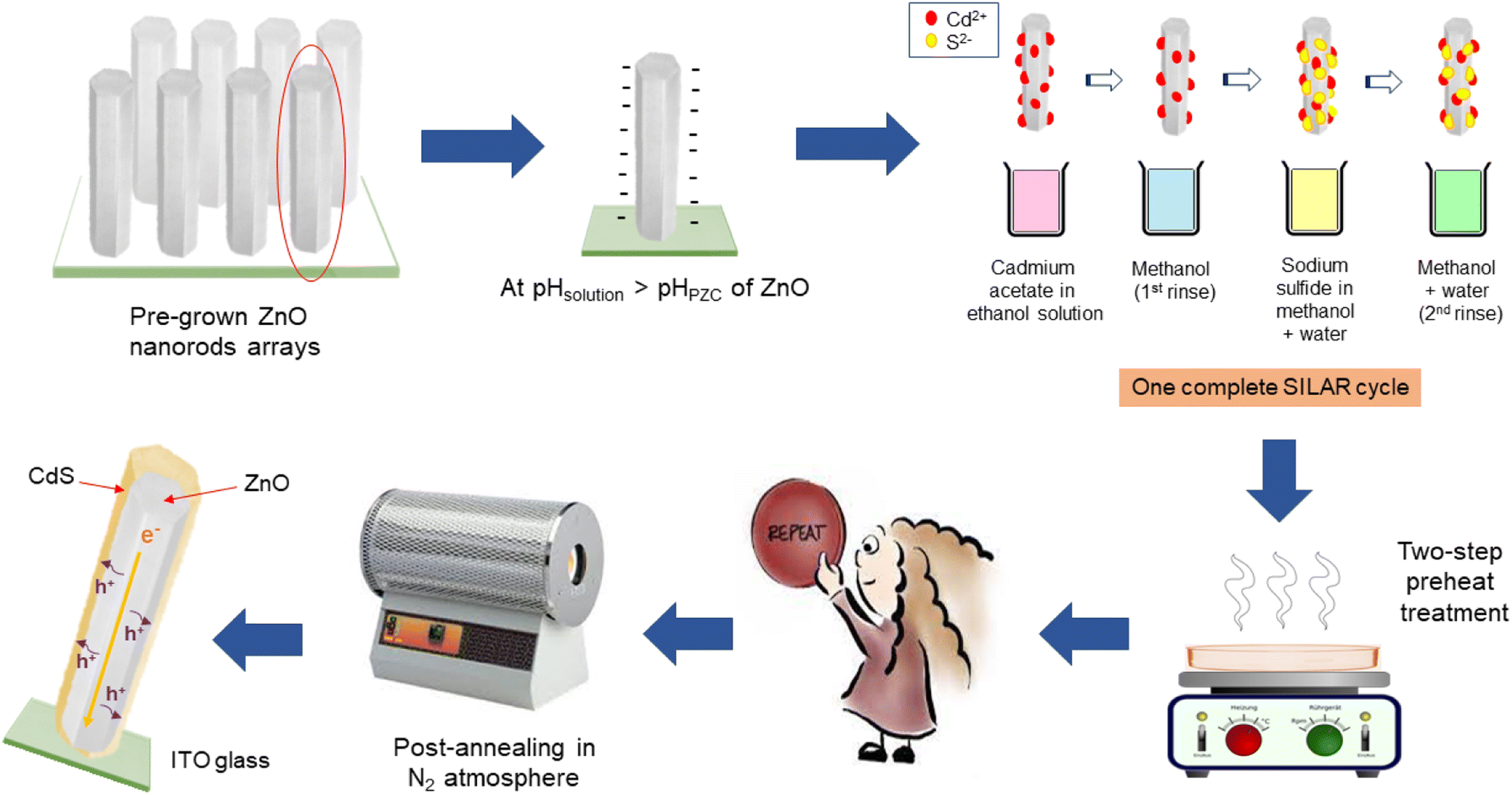
Details of high-quality vertically aligned ZnO NRs arrays formation on seeded indium tin oxide (ITO, 20 ohm/sq) glass have been reported in previous work.22 To develop a ZnO NRs/CdS heterostructure, the ITO/ZnO NR photoanode was first dipped in 0.16 M cadmium acetate dihydrate (Cd(CH3COO)2·2H2O, purity 98%, Merck, CAS no. 5743-04-4) ethanolic solution for 30 s to allow the adsorption of Cd2+ ions, followed by rinsing for 30 s using methanol (CH3OH, AR grade, Chemiz, CAS no. 67-56-1). The reaction was continued with the subsequent immersion in anionic precursor in which equimolar sodium sulfide was dissolved in a 1![[thin space (1/6-em)]](https://www.rsc.org/images/entities/char_2009.gif) :1 volume ratio of deionized water and methanol. Again, the substrate was rinsed to remove excessive or unreacted S2− ions using a mixture of deionized water and methanol (also a 1:1 volume ratio). The mixture solvent was selected here instead of using plain deionized water due to the lower dielectric constant but higher wettability of ethanol (C2H5OH, EMSURE®ACS, ISO, Reag. Ph Eur grade, Merck, CAS no. 64-17-5), and better Na2S solubility in the mixture23 could promote ion adsorption, reaction and distribution on the core semiconductor. The prepared samples were then subjected to a 10 minute drying process at 150 °C, followed by another 10 minutes of preheating treatment at 250 °C using a hotplate. The reaction-dipping steps were repeated 5, 7, 10, 13 and 15 times to achieve different CdS thicknesses. Later, the pH of the cationic solution was varied from ∼4.7 to ∼8.7 to determine a suitable environment for CdS nanocrystal growth while maintaining the stability of ZnO NRs arrays. Lastly, the effects of different post-annealing temperatures were studied in the range from 300 °C to 600 °C where a complete transformation from the cubic to the hexagonal phase of CdS could occur.24 A nitrogen atmosphere was required for the annealing process in the furnace due to the easy oxidation of CdS.25 The schematic diagram for CdS deposition is displayed in Fig. 1.
:1 volume ratio of deionized water and methanol. Again, the substrate was rinsed to remove excessive or unreacted S2− ions using a mixture of deionized water and methanol (also a 1:1 volume ratio). The mixture solvent was selected here instead of using plain deionized water due to the lower dielectric constant but higher wettability of ethanol (C2H5OH, EMSURE®ACS, ISO, Reag. Ph Eur grade, Merck, CAS no. 64-17-5), and better Na2S solubility in the mixture23 could promote ion adsorption, reaction and distribution on the core semiconductor. The prepared samples were then subjected to a 10 minute drying process at 150 °C, followed by another 10 minutes of preheating treatment at 250 °C using a hotplate. The reaction-dipping steps were repeated 5, 7, 10, 13 and 15 times to achieve different CdS thicknesses. Later, the pH of the cationic solution was varied from ∼4.7 to ∼8.7 to determine a suitable environment for CdS nanocrystal growth while maintaining the stability of ZnO NRs arrays. Lastly, the effects of different post-annealing temperatures were studied in the range from 300 °C to 600 °C where a complete transformation from the cubic to the hexagonal phase of CdS could occur.24 A nitrogen atmosphere was required for the annealing process in the furnace due to the easy oxidation of CdS.25 The schematic diagram for CdS deposition is displayed in Fig. 1.
 |
| | Fig. 1 Preparation of the ZnO NRs/CdS photoanode. | |
2.2 Characterization and measurement
The structural, morphological, optical and photoelectrochemical properties of prepared ZnO/CdS nanostructures were investigated through in-depth characterizations. X-ray diffraction (XRD) was performed using a Panalytical X'Pert Pro with Cu Kα radiation (λ = 1.54 Å) in the 2θ range of 20°–60° and at a grazing angle of 0.5° to analyze the crystalline structure of materials. The crystal phase of CdS was further confirmed using a Witec Alpha 300R Plus Confocal Raman Microscope with a 488 nm laser. A field emission scanning electron microscope (FESEM, JEOL JSM-7600F) with Energy Dispersive X-ray Spectroscopy (EDX) was used to identify the surface morphology and elemental composition of the fabricated thin films. X-ray photoelectron spectroscopy (XPS) studies were done on a Scanning X-ray Microprobe Phi Quantera II/Ulvac-Phi XPS model using an Al target as the X-ray source while high-resolution transmission electron microscopy (HRTEM) with selected-area electron diffraction (SAED) was performed using a Tecnai F20 microscope to further confirm the crystalline characteristics and lattice fringes of the deposited thin films. The absorbance of each photoelectrode was characterized using a Shimadzu UV-2600 ultraviolet-visible (UV-Vis) spectrophotometer within the range of 200–800 nm. Linear sweep voltammetry (LSV) and electrochemical impedance spectroscopy (EIS) were performed at room temperature with the ZnO/CdS heterostructure, Ag/AgCl and Pt wire acting as the working electrode, reference electrode and counter electrode, respectively. The photocurrent dependence on the voltage (I–V) was measured in an aqueous solution of 0.10 M sodium sulfide (Na2S·xH2O) and 0.10 M sodium sulfite (Na2SO3) under intermittent halogen lamp irradiation (100 mW cm−2). Herein, S2− and SO32− ions are indispensable as hole scavengers to prevent self-oxidation of the CdS layer.
3 Result and discussion
3.1 The growth mechanism and preliminary investigation of the preheating treatment effect
It has been widely reported that the formation of chalcogenide thin films can take place through an ion-by-ion, hydroxide aggregation or cluster-by-cluster mechanism. The ion-by-ion mechanism (heterogeneous reaction) generally leads to uniform, crystalline and compact CdS films with hexagonal or mixed (hexagonal and cubic) phases, while the cluster-by-cluster mechanism (homogeneous reaction), which allows colloidal particle precipitation prior to deposition, usually results in porous, non-uniform and poorly adherent CdS films.26,27 Typically, the SILAR process favours the nucleation and growth of CdS films by adopting the ion-by-ion mechanism in which every step was introduced by Pathan and Lokhande in 2004.28 When the developed ZnO NRs were immersed in a cationic ethanolic solution, a high concentration of positively charged cadmium ions were attached to ZnO NRs via van der Waals and electrostatic forces, thus resulting in a positive (inner) Helmholtz double layer while the negatively charged counterions (acetate) formed the outer Helmholtz layer. The acetate ions played the role of a weak base and induced a pH of ∼6.1 (dependent on concentration) in Cd(acetate)2-dissolved solution to assist CdS adsorption and reaction.29 The first rinse in the ion-exchanged solution (ethanol) removed loosely bound or excess adsorbed Cd2+ from the diffusion layer to allow a saturated electrical double-layer formation. As an alternative to the aqueous medium, alcohol can stabilize the ionic solutions and restrict cadmium hydroxide formation.30 Furthermore, the anti-solvent effect generated by the insoluble nature of Cd acetate in ethanol solvent additionally propelled the Cd2+ ions towards the substrate for contact, therefore, increasing the ion adsorption.29 In the third step, the immersion in the anionic precursor (Na2S solution), HS−, S2−, OH− and Na+ ions diffused from the solution bath in the diffusion layer towards the solid solution interface until equilibrium was established. The HS− and S2− entered the outer Helmholtz layer and reacted with pre-adsorbed Cd2+ to form the CdS nanoparticles monolayer. Lastly, the second rinse removed any unreacted species and unwanted by-products from the diffusion layer. By repeating such deposition cycles under controlled parameters, the heterogeneous nucleation grew into a continuous CdS film with appropriate thickness and morphology. The interaction scheme in the formation of CdS particles is summarised in (eqn (1)–(4)).| | |
Cd(CH3COO)2 → Cd2+ + 2CH3COO−
| (1) |
| | |
Na2S + H2O → 2Na+ + SH− + OH−
| (2) |
| | |
SH− + OH− → S2− + H2O
| (3) |
Directly varying the pH of the precursor solution could also affect the interaction and growth behaviour among reacting particles and, therefore, their adsorption degree onto the adsorbent surface as schemed in Fig. 2.
 |
| | Fig. 2 A quick view of the effect of pH on nanoparticle agglomeration behaviour. | |
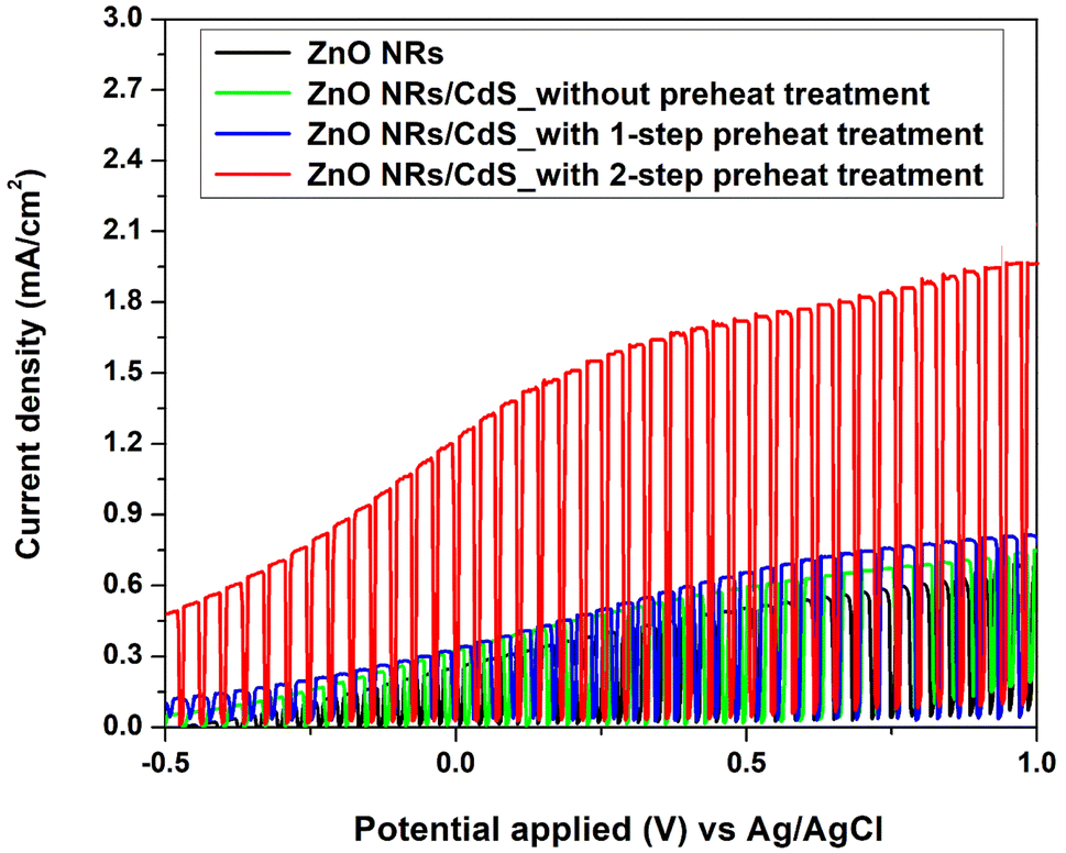
Generally, a low-temperature pre-treatment applied during the thin film deposition process is crucial for evaporating the organic solvent and leaving only the desired particles on the substrate surface. The effective removal of solvent and impurities enables uniform nuclei distribution and faster grain formation to promote the hexagonal phase crystal arrangement in the preferred orientation. This facilitates crystallization in subsequent post-heat annealing (at a higher temperature) and the reduction of grain boundaries to extensively increase the nanofilm quality and charge carrier mobility. To confirm the hypothesis, different preheating conditions were compared using linear sweep voltammetry (Fig. 3) and finally, a two-step preheating treatment at 150 °C and 250 °C was chosen to fabricate all binary photoanodes due to the promising photocurrent enhancement. More in-depth study is ongoing to provide a clearer picture of the preheating-assisted SILAR technique and examine the possibility of surface oxidation or secondary material formation under this proposed preheating process to avoid the localization of the oxygen state at the ZnO/CdS interface, which might affect the PEC cell efficiency.
 |
| | Fig. 3 The effect of the preheating treatment on photocurrent generation. | |
3.2 Morphology and compositional analysis
The SILAR-coated ZnO/CdS photoelectrodes with increasing layer numbers displayed a tendency to change into a deeper yellow colour, which indicated that more CdS was successfully deposited onto ZnO NRs and increased the film thickness. Fig. 4 shows the typical surface FESEM images of bare ZnO NRs and CdS-sensitized ZnO NRs for comparison. Hydrothermally grown ZnO NRs arrays were vertically aligned on a seeded substrate with a smooth surface and reported a diameter of about 69 nm. Microscopically, the deposition of CdS NPs retained the ZnO morphology without affecting the rod diameter much. However, the surface roughness increased after CdS sensitization as one-dimensional ZnO NRs provided sufficient anchoring sites. Spherical CdS nanoparticles were homogeneously distributed on the hexagonal ZnO surface with the average particle size increasing from 10.8 nm to 22.1 nm along with the increasing SILAR cycle number. At the early stage of nucleation, small-sized CdS particles were mainly observed. On increasing the thickness up to 10 SILAR cycles, CdS NPs tended to agglomerate into larger grains and slowly block beneath the NRs surface, especially on reaching 15 deposition layers. According to the cross-sectional images (Fig. 4a and e inset), CdS NPs were closely embedded and formed a rough shell over the surface of the nanorods. Nevertheless, pristine ZnO NRs arrays and the heterostructure decorated with 13 layers of CdS depicted the film thickness of 1.79 μm and 1.83 μm, respectively.
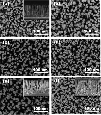 |
| | Fig. 4 Plane view FESEM images of bare ZnO nanorods (a), and ZnO NRs/CdS deposited on ITO substrates after different numbers of SILAR cycles: 5 (b), 7 (c), 10 (d), 13 (e) and 15 (f). The insets are the corresponding cross-section images. | |
The effect of modifying the pH of the cationic solution from 4.7 to 8.7 on the morphology of the CdS layer is displayed in Fig. 5. The micrographs show that pH significantly affected the size and distribution of grown nanoparticles. Although most of the particles tend to agglomerate in nature, large aggregates on the ZnO nanorod surface were only observed for the films deposited at lower and higher pH values. Theoretically, the relationship between the nanoparticle agglomeration behavior and solution pH can be discussed based on the changes in ionic strength and potential barrier (electrostatic repulsive forces). Nanoparticle collision in colloidal suspensions may lead to agglomeration and aggregation where the occurrence rate can be decreased through the electrostatic stabilization method by creating surface charge around the suspended particles.31 According to Saxena and co-workers, CdS NPs are highly stable above pH 6.12.32 Faster agglomeration was therefore observed at lower pH due to the unstable dispersion and coalescence of primary particles into flower-like clusters. In addition, protons (H+ ions) from HCl caused ZnO dissolution and competed with Cd2+ in occupying the adsorption sites on the ZnO surface, which resulted in low CdS deposition in acidic solution due to electrostatic repulsion. By increasing the pH value of the cationic precursor to 5.7, the suspension stability was improved, and the agglomeration rate was significantly reduced with the apparent particle size decreasing from 28.2 nm to 22.4 nm as approximated using the Image J software. The effect of pH on CdS NPs deposition was further investigated by changing the initial pH of the cadmium acetate ethanolic solution to pH 7.7 and pH 8.7. In this section, the adsorption capability is modulated by the chemical reaction between the surface of ZnO NRs and the surrounding precursor medium. The point of zero charge (PZC) of ZnO NRs is ∼pH 6.5.33 This means that when the pH of the cadmium cation (Cd2+) solution is above pH 6.5, the surface of ZnO will bear a negative charge, which is feasible for positively-charged Cd ion adsorption.29 All ZnO/CdS thin films prepared at conditions above the pHPZC of ZnO NRs illustrated a more regular grain size despite aggregates still being observed when the pH was further increased. Faster secondary particle growth over the pre-grown CdS particles, which act as secondary nucleation sites, caused isolated CdS particle formation instead of ZnO NRs/CdS core–shell structures. Therefore, the initial pH of 6.7 of the cadmium acetate precursor remained for subsequent studies to prevent any possible etching of ZnO NRs when the nanorod arrays were in contact with a highly basic aqueous solution.34
 |
| | Fig. 5 The morphologies of ZnO NRs/CdS samples synthesized in the cationic solution at pH 4.7 (a), pH 5.7 (b), pH 6.7 (c – original pH value), pH 7.7 (d) and pH 8.7 (e). Planar and cross-section images of ZnO NRs/CdS annealed at 500 °C (f). | |
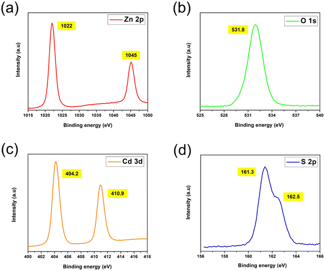
In the post-annealing process, the mobility of the atoms within the crystal allowed them to move into more stable positions with minimum internal energy;35 for instance, a stacked arrangement as seen in the FESEM image of the sample annealed at 500 °C (Fig. 5f). In this case, the CdS nanoparticles adopted sharper edges and grew into larger spherical clusters, which in turn caused strain relaxation.15 It is worth noting that the yellow colour of the CdS layer faded after being annealed at 600 °C. EDX analysis was thus performed to compare the components of binary photoelectrodes that underwent post-heating treatments at 300 °C, 500 °C and 600 °C, respectively. As depicted in Fig. 6a–c, there was no major stoichiometric variation across the surface of deposited films when the annealing temperature increased from 300 °C to 500 °C, but a reduction of the Cd:S weight percentage ratio was observed at 600 °C, suggesting the initiation of the material loss of Cd or S elements, which was disclosed by Colorado and co-workers36 with CdS nanoparticle degradation in an argon atmosphere at 600 °C using TGA and XRD experiments. An annealing atmosphere of 600 °C may have been extreme for CdS-sensitized ZnO heterostructures in this study when considering the evaporation temperature of Cd (500 °C) and S (600 °C) elements.37,38 Fig. 6d and e shows the transmission electron microscope (TEM) and high-resolution TEM (HRTEM) images of ZnO/CdS annealed at 500 °C. Consistent with earlier discussions, the homogeneous coating of the CdS layer on ZnO nanorods with an even thickness of ca. 10 nm again confirmed the core–shell nanostructure formation. The well-resolved two-dimensional lattice fringes with spacings of 0.27 nm, 0.2 nm and 0.21 nm correspond to the (002) plane of ZnO, and the (103) and (110) planes of CdS. Meanwhile, the obtained SAED pattern (Fig. 6f) with regular concentric rings in different radii revealed the polycrystalline nature of the prepared thin film sample, which agrees with the XRD results. The CdS crystal size distribution plot is presented in Fig. 6g, and their average size estimated from the TEM micrograph was found to be 5.71 nm. Fig. 7a–d demonstrates the high-resolution core spectra of Zn 2p, O 1s, Cd 3d and S 2p analysed using X-ray photoelectron spectroscopy (XPS). The strong peaks located at 1022 eV and 1045 eV were attributed to Zn 2p3/2 and Zn 2p1/2,5 while those observed at 404.2 and 410.9 eV perfectly fit the Cd 3d doublets (Cd 3d5/2 and Cd 3d3/2).2 Concerning the XPS spectra of O 1s, the peak observed at 531.8 eV was consistent with the oxygen-deficient surface of ZnO NRs that were covered by the CdS layer.25 The peak positions of S 2p states were found at 161.3 eV and 162.5 eV, similar to the findings reported by Velanganni et al.7 and Mendhe et al.8 These results confirmed the chemical states of Zn2+, O2−, Cd2+ and S2−.
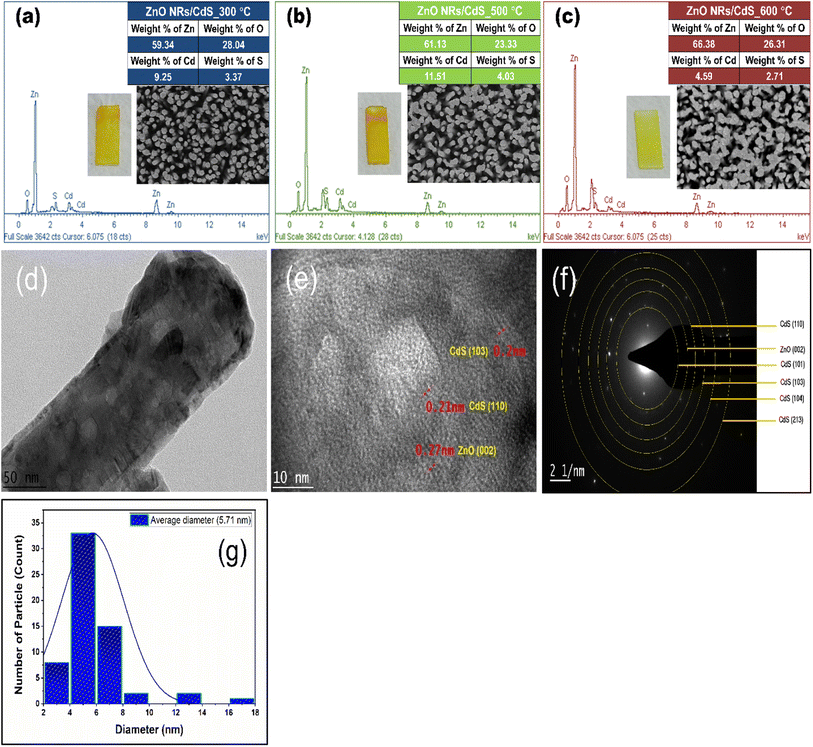 |
| | Fig. 6 Elemental composition analysis (with FESEM images and sample photographs) of ZnO NRs/CdS samples annealed at 300 °C (a), 500 °C (b) and 600 °C (c), respectively. Plane view TEM micrograph (d), HRTEM image (e), SAED pattern (f), and histogram of crystal size distribution (g) of the optimal ZnO NRs/CdS core–shell heterostructure annealed at 500 °C. | |
 |
| | Fig. 7 XPS spectra corresponding to Zn-2p (a), O-1s (b), Cd-3d (c), and S-2p (d). | |
3.3 XRD and Raman structures
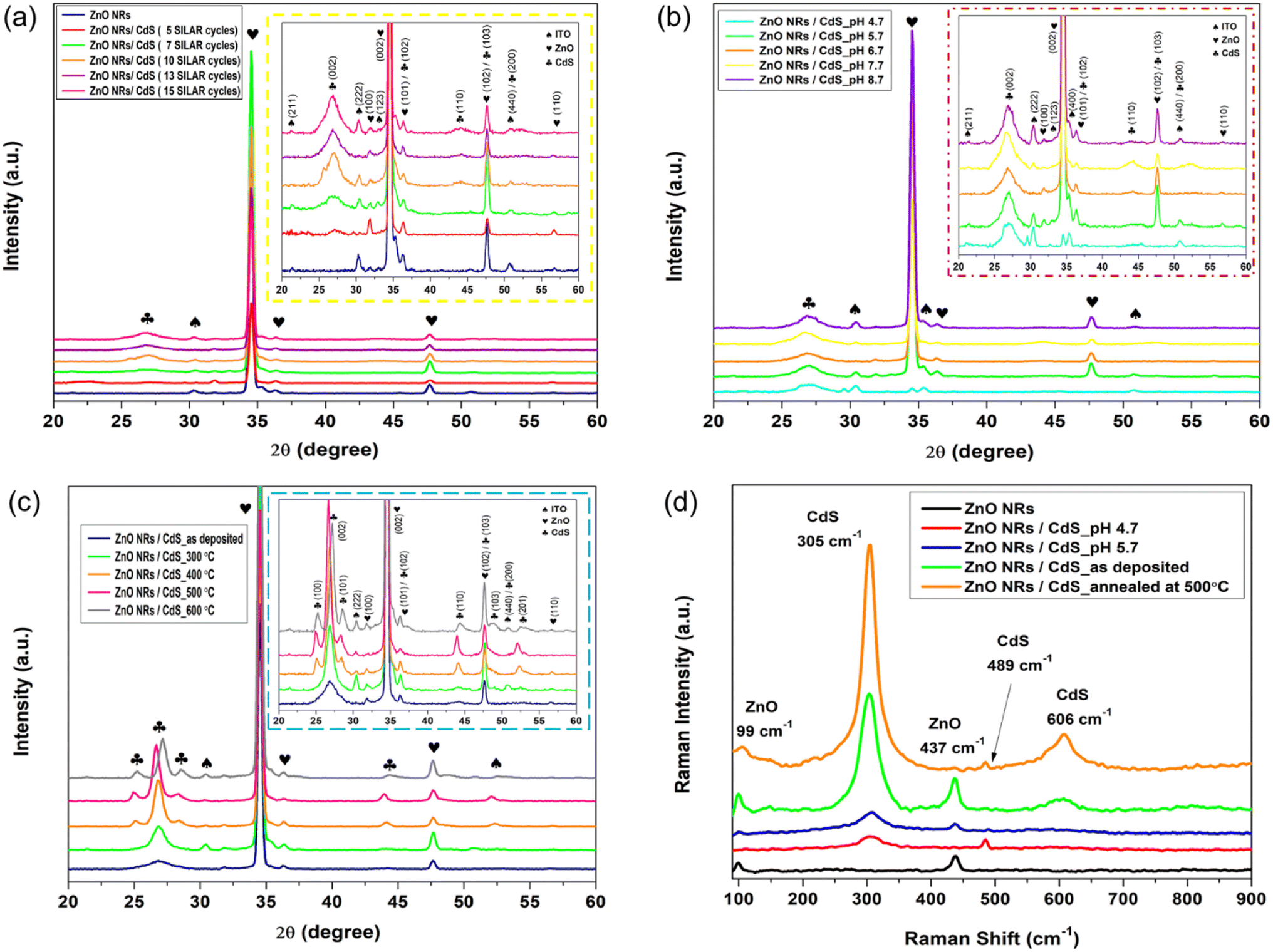
Fig. 8a shows the XRD patterns of prepared heterojunction thin films of different CdS thicknesses with the inclusion of ITO as a reference (JCPDS 01-089-4598). The scanning step resolution was fixed at 0.08°. The diffraction pattern revealed the polycrystalline nature of all prepared samples in which the dominant peaks found at 2θ = 31.9°, 34.5°, 36.3° and 47.6° originated from the standard wurtzite ZnO phase (JCPDS 00-065-3411). The preferred orientation observed in the (002) direction is due to the minimum surface free energy that promotes the nucleation process. From the inset, the reflections observed at 26.7° and 43.7° corresponding to (002) and (110) planes confirmed the formation of hexagonal CdS NPs (JCPDS 01-077-2306). Similar findings have been reported in the literature.39,40 Interestingly, the sharp (002) peak of ZnO gradually reduced in intensity with the enhancement of the CdS peak as the SILAR deposition increased from 5 to 15 cycles. A higher SILAR cycle number typically increases the deposition and growth rates of CdS NPs followed by a higher chance for the atoms to be arranged into greater crystalline order.41 Therefore, it is understood that the film crystallinity was increased along with grain size for thicker CdS layer formation. In this context, a more intense (002) peak positioned at 2θ = 26.7° was selected to estimate the crystallite size (D) of CdS by employing the well-known Scherrer formula: D = 0.9λ/βcos(θ), where λ is the wavelength of X-ray radiation, β is the full width at half maximum and θ is the diffraction angle. The calculated D values were 5.54 nm, 5.60 nm, 5.91 nm, 6.26 nm and 6.88 nm for 5, 7, 10, 13 and 15 SILAR cycles. Considering the different surface mobilities of the adsorbed species and growth kinetics, the pH of the aqueous medium plays a vital role in affecting the crystalline quality of the deposited CdS thin films. In Fig. 8b, the peak associated with the (002) plane at 2θ = 26.7° did not vary much in intensity but two characteristics peaks of ZnO located at 34.5° and 47.6° decreased with increasing pH, indicating a negative effect on corresponding crystal structures. At pH 4.7, in particular, both fingerprints were relatively weak or undetectable. Few noticeable ITO substrate peaks showed inhomogeneous particle distribution and less compact film formation at pH 4.7, 5.7 and 8.7. Interestingly, a new diffraction peak at 2θ = 52.2° was found in the film prepared at pH 7.7. Together with the diffraction peaks observed at 2θ = 26.7° and 43.9°, it was assumed that the cubic CdS phase was formed15 at pH 7.7. Representative XRD diffraction patterns of CdS-decorated ZnO NRs, both as-deposited and annealed with nitrogen gas flow at different temperatures, are shown in Fig. 8c. Upon annealing, the sharpness of the (002), (110) and (103) peaks were significantly increased due to the enhanced crystallinity of CdS nanostructures with the retained wurtzite crystal structure of ZnO NRs. The appearance of shoulder-like peaks at 24.8° and 28.2° belonging to the (100) and (101) reflection planes again confirmed the presence of hexagonal CdS. This result is well in agreement with previous reports as a thermodynamically more stable hexagonal phase is invariably formed when heated above 300 °C.15 Along with the changes in annealing temperature, few additional small peaks are sometimes observed at 2θ = 48.7°, 50.8° and 52.8° probably due to recrystallization and phase transformation occurring in the growing film.42 All CdS diffraction peaks, especially the (002) plane, shifted to a higher angle when the annealing temperature reached 600 °C, accounting for the compressive or tensile strains and the presence of defects in the developed film as reported in ref 43. The structural strain and dislocation density as a function of different annealing temperatures were determined using the following eqn (5) and (6):| |
 | (5) |
| |
 | (6) |
 |
| | Fig. 8 XRD patterns (a–c) and room-temperature Raman scattering spectra (d) of pristine ZnO NRs and ZnO NRs/CdS nanostructures prepared at different SILAR parameters. The insets show the enlarged evolution for better XRD diffraction peak observation. | |
Referring to Table 1, a decline in strain value and dislocation density implies a reduction in lattice imperfections (structural defects) and consequently, larger crystallite size and higher crystallinity levels for the crystal geometry would be obtained after appropriate post-heat treatment.44
Table 1 Parameters obtained from XRD analysis of the as-deposited and annealed ZnO NRs/CdS photoanodes
| Annealing temperature |
Crystallite size (nm) |
(002) peak angle |
FWHM |
Strain (×10−3) |
Dislocation density (×10−2) |
| As-deposited |
6.26 |
26.7 |
1.3046 |
5.53 |
2.55 |
| 300 °C |
9.43 |
26.8 |
0.8659 |
3.67 |
1.12 |
| 400 °C |
12.97 |
26.8 |
0.6298 |
2.67 |
0.59 |
| 500 °C |
14.80 |
26.8 |
0.5510 |
2.34 |
0.46 |
| 600 °C |
11.50 |
27.1 |
0.7085 |
3.01 |
0.76 |
As documented in the literature, the argument on the purity and composition of fabricated CdS thin film could always arise due to the similar diffraction among cubic CdS, hexagonal CdS, ZnO and the FTO substrate.25,45 To provide a better explanation and clear evidence for the crystal structure of the formed CdS, Raman spectroscopy was also applied in this work and selected spectra are illustrated in Fig. 8d. For the bare ZnO NR photoanode, a weak peak at 99 cm−1 and a prominent peak at 437 cm−1 were observed and assigned to nonpolar E2 (low) and E2 (high) phonon modes. The peak at 437 cm−1 is associated with the strong wurtzite crystal orientation and good alignment of ZnO NRs perpendicular to the substrate.46 Meanwhile, a strong peak at 305 cm−1 and a weaker peak at 606 cm−1 represent the first-order longitudinal-optical (1LO) phonons and second-order longitudinal-optical (2LO) phonons of hexagonal CdS. The coexistence of these two characteristic peaks indicates the high crystallinity of the as-deposited CdS NPs. No peak belonging to cubic CdS was observed at 243 cm−1, therefore confirming that the prepared CdS layers were in a stable hexagonal phase.25 However, the ZnO/CdS photoelectrodes fabricated at pH < 6.7 presented lower Raman peak intensity at 305, 437 and 606 cm−1, which could be a result of severe nanocrystallite degradation in acidic media. The increment of both 1LO and 2LO band intensities after the annealing step was rationalized by the transition from non-resonant to resonant Raman scattering.47 A smaller FWHM or narrowing of the 1LO peak implies larger crystallite size and increasing crystallinity when post-heat treatment at 500 °C is sufficient to remove the cubic phase of CdS, as supported by XRD and FESEM analysis. The Raman observations of Rokade et al.48 and Jiang et al.49 regarding the structural analysis agree well with the presented results.
3.4 Optical absorbance spectra and bandgap determination
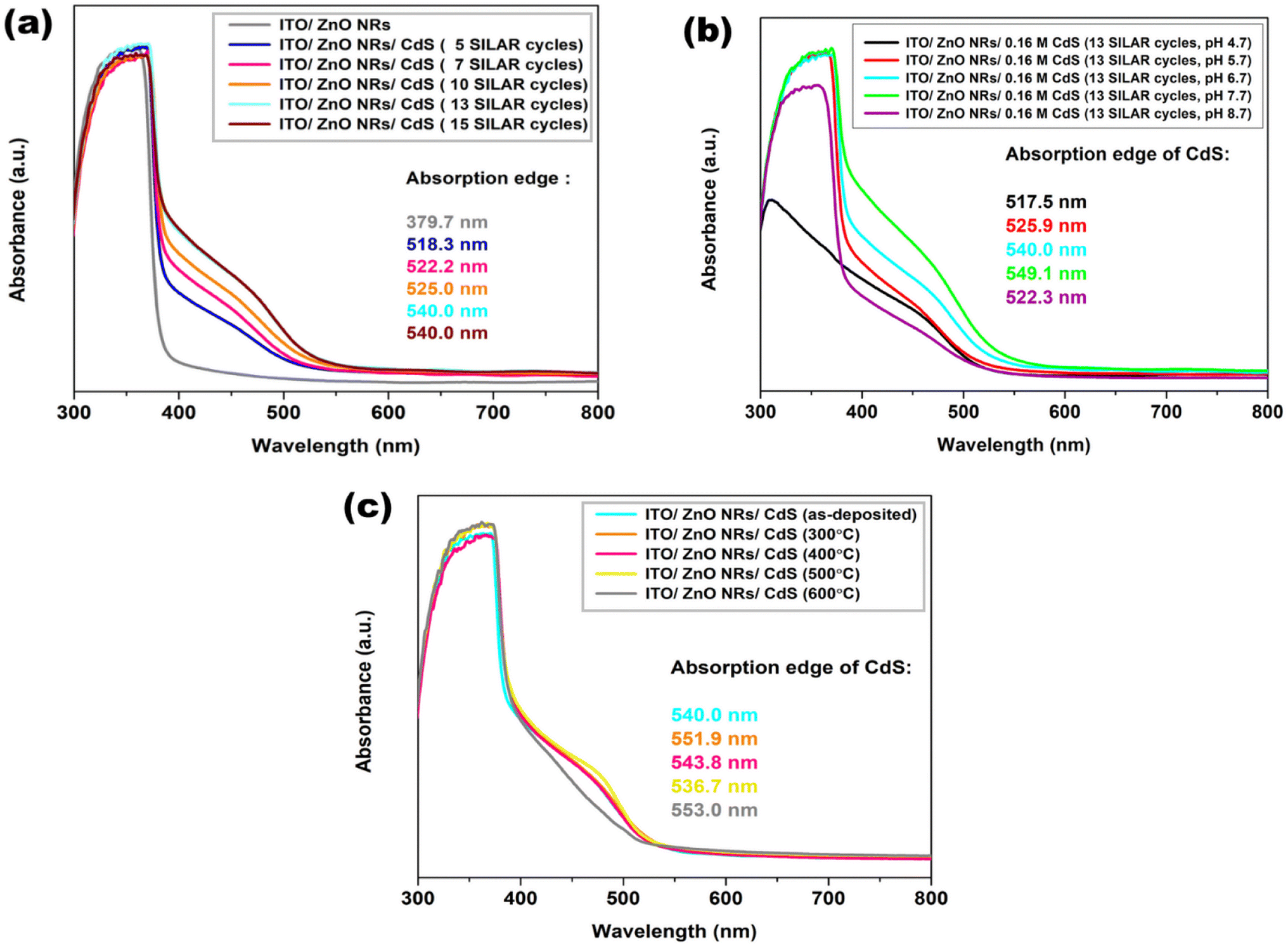
Light absorption capability is highly dependent on the thickness of the semiconductor with the consideration that the deposited layer should invariably be thicker than the incident light penetration depth.50 A thicker film could certainly absorb more incident light for exciton generation but in some cases, it increases the series resistance and reduces the photocurrent. In contrast, a severe optical loss could take place in an ultrathin film layer due to strong light transmission but poor light absorption, trapping and collection.51 In addition, pinholes and current leakage can occur in thin-layered photoelectrodes due to the non-uniformity of the surface coverage.52 Therefore, an optimum thickness is highly required to construct a high-quality photoanode. The absorption behaviour of ZnO/CdS samples with different immersion numbers was recorded as a function of wavelength (Fig. 9a). Bare ZnO NRs mainly exhibited a band-edge exciton at 380 nm, while for CdS coated ZnO NRs (13 cycles), the optical absorbance was enhanced and the absorption edge was significantly red-shifted to 540 nm. The observed threshold is in good agreement with the narrower bandgap of CdS that can expand excitonic absorption to the visible region as compared to that of ZnO NRs arrays. Broadening of the absorption peak also confirmed the presence of CdS sensitizers and the delocalization of electrons across the core/shell interface.53 By noting the absorption maxima, the CdS crystallite size can also be determined using the empirical fitting function in eqn (7):30,54| | |
DCdS = (−6.6521 × 10⁻⁸)λ3 + (1.9557 × 10⁻⁴)λ2 − (9.2352 × 10⁻²)λ + (13.29)
| (7) |
 |
| | Fig. 9 UV-Vis absorption spectra of ZnO NRs/CdS nanostructures as a function of SILAR cycle (a), pH (b) and annealing temperature (c). | |
D represents the crystallite size (nm) and λ represents the wavelength (nm) where the excitonic absorption of CdS nanocrystals reached an extreme point. Herein, the calculated CdS crystallite sizes closely resemble the values determined from the Scherrer formula in the range of 4.83–6.19 nm. Apart from film thickness, the surface roughness, nanoarchitecture and particle distribution are also important factors that could change the light scattering, absorption, and trapping ability. Fig. 9b demonstrates the absorption spectra of ZnO NRs/CdS photoelectrodes deposited at pH values of 4.7, 5.7, 6.7, 7.7 and 8.7. From observation, the absorbance value increased with increasing pH values since the adequate CdS loading on the more negatively-charged ZnO NRs surface and higher film roughness enabled greater light scattering.26 Visible-light absorption was less effective at pH 5.7 due to the smaller active area of the granule-like CdS morphology but the excessive agglomerates observed at pH 4.7 and pH 8.7 blocked the surface of the ZnO NRs arrays and existing pores of the film layer, creating a barrier to light irradiation and electrolyte infiltration and thus, hampered the optical properties of the binary photoanode. The post-annealing process is effective at optimizing the optical behaviour of the heterostructured photoanode by improving the crystal properties without affecting their surface morphology much. From the absorption spectra presented in Fig. 9c, it can be inferred that identical absorbance was detected for annealing temperatures of 300–500 °C. At 600 °C, the decrement of visible light absorption was probably because of sulfur deficiency defects as a result of the evaporation of S from the CdS layer. Overall, the absorbance edge, with regard to the threshold of charge transition between the highest nearly filled band and the lowest nearly empty band,55 was blue-shifted toward a lower wavelength. This is similar to the studies by Mohammed et al.56 and Bashar et al.57 on the effects of increasing the annealing temperature, and this observation can be explained by the increasing amount of cadmium and sulfur since annealing triggered film densification and great improvement in the crystallinity.
Based on the absorption spectra, the effective band gaps of ZnO NRs and ZnO NRs/CdS core–shell thin films can be derived through Tauc plot using eqn (8) and extrapolating the linear portion of the curves of (αhν)2 versus (hν).
| |
 | (8) |
Fig. 10 presents the direct allowed transition (where n = 1/2) of all ZnO/CdS thin films. In Fig. 10a, a lower band gap (Eg) was observed for higher CdS deposition cycles, attributed to the increased particle size as supported by FESEM images. The estimated optical band gap value was 2.42 eV for the as-deposited sample and reached 2.45 eV for films annealed at 500 °C (Fig. 10b). After annealing at 600 °C, the obtained energy bandgap was found to deviate more from that of bulk CdS and approached a higher value of 2.50 eV. This could be due to material loss as the evaporation of surface CdS diminished their sensitization effect. In this context, the optical bandgap of the annealed binary photoanode tends to gradually switch to the pristine ZnO NRs, agreeing with the weakening of visible light absorption.
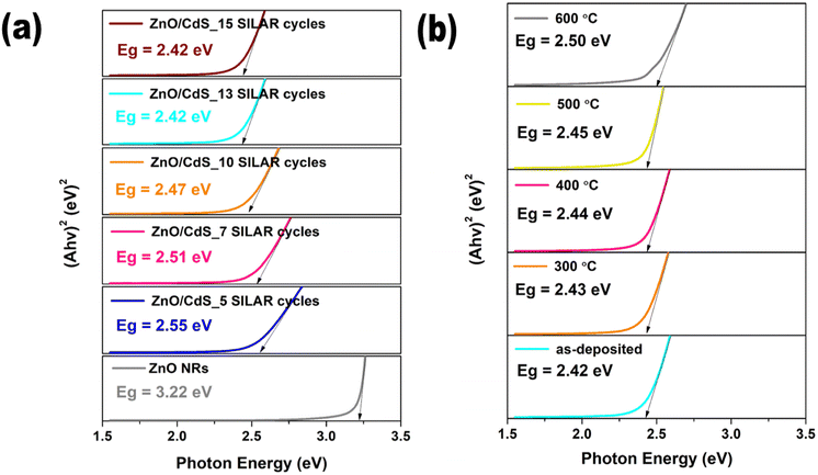 |
| | Fig. 10 Bandgap energy curves of ZnO NRs/CdS heterostructures prepared at different dipping cycles (a) and annealing temperature (b). | |
3.5 Photoelectrochemical properties
Since all nanostructured ZnO/CdS photoanodes displayed enhanced optical behaviour and crystallinity as compared with ZnO NRs, it is believed that the fabricated nano-heterojunction can contribute to high photoelectrochemical performance under solar-simulated light. Using bare ZnO NRs and CdS-sensitized ZnO NRs as the working electrodes, the effectiveness of CdS NPs as photosensitizer was studied through current density–voltage (J–V) plots presented in Fig. 11. The photocurrents increased with increasing applied anodic potential, representing typical n-type semiconductor behavior because both ZnO and CdS are n-type semiconductors. As an overall observation, increasing the SILAR cycle number, pH and annealing temperature resulted in the steady growth of the photocurrent density (Jph) in the ZnO/CdS core–shell structure. For low immersion cycles (5 cycles and 7 cycles) where a small amount of CdS NPs just started to be adsorbed onto the ZnO NRs arrays by van der Waals and electrostatic forces,30 the improved photo-response was mainly due to the extended optical absorption range and higher electron–hole pair generation. Likewise, the continual growth of the photocurrent density from 2.638 to 3.917 mA cm−2 was observed with further augmentation of the layer thickness for up to 13 cycles. This phenomenon is highly attributed to the improved film crystallinity with suitable shell thickness that matches the minority carrier diffusion length to inhibit the recombination of photo-generated electrons under light illumination,58 which effectively enhanced the PEC performance. However, Jph deteriorated with 15 SILAR cycled nanoparticles as their agglomeration on the surface of the nanorods blocked the active sites and empty spaces between neighbouring nanorods, preventing suitable light and electrolyte penetration from reaching the core ZnO NRs arrays.54,59,60
 |
| | Fig. 11 Linear sweep voltammograms obtained at the scan rate of 20 mV s−1 at applied potentials from −0.5 V to +1.0 V (vs. Ag/AgCl) under illumination intensity of 100 mW cm−2 for different thicknesses (a), pH (b) and annealing temperatures (c) of CdS-sensitized ZnO NRs. | |
A similar issue was also detected when the applied pH of the cationic precursor was less appropriate for homogeneous CdS deposition. As expected, a higher loading amount of CdS NPs generated a higher photocurrent density. However, the high density of surface aggregates at pH 4.7 and pH 8.7 led to a strong deviation of photocurrent. The existence of grain boundaries prevented efficient charge transport45 since higher potential barriers at boundaries triggered light absorption at higher energies. The widening of the band gap, therefore, hardened the electronic transition between the conduction and valence bands of cadmium sulfide. Besides that, the degradation of the ZnO NRs structure when in contact with highly acidic and alkaline media might limit the light scattering effect and shorten the optical path length. This in turn interferes with the directional electron transport in 1D ZnO NRs and charge collection at the ZnO/CdS interface. Better electronic performance of ZnO/CdS nanostructures was observed only at pH 6.7 and pH 7.7. A slightly lower photoelectrochemical performance for thin film synthesized at pH 7.7 was ascribed to lower crystallinity. In addition, the transparent cationic precursor slowly turned milky with the addition of 0.1 M sodium hydroxide (NaOH) to increase its alkalinity. The formation of any hydroxides or complexes with the cadmium ions was, therefore, possible, which could compete with the CdS NPs adsorption.
Pristine ZnO NRs and as-deposited ZnO NRs/CdS demonstrated photocurrent densities of only 0.483 mA cm−2 and 3.917 mA cm−2, respectively, at the applied potential of 0.5 V versus Ag/AgCl. With post-heat treatment at increasing temperatures up to 500 °C, the photocurrents were further boosted from 4.082 mA cm−2 to 5.441 mA cm−2 as seen in Fig. 11c, suggesting the higher photosensitivity of the CdS shell and efficient charge separation in the heterostructure. Generally, a polycrystalline film is highly disordered with a large number of grain boundaries. In this case, the electronic transport mechanism is dominated by the random hopping steps of electrons along the grain boundary or by diffusion through extended states. The trapping centers that exist at grain boundaries can capture free carriers and therefore strongly affect the carrier transport properties.35,44 Better crystallinity in the annealed films and an increment in the crystallite size improve the conductivity and optical reflectance44 and decrease film resistivity, and also accelerate the charge collection in the whole system and minimize the recombination losses between ZnO NRs and the electrolyte61 so that electrons can successfully reach the counter electrode for further reaction. A huge difference between the measured dark and saturated photo currents supports the efficient charge separation, transportation and collection accessed by good-quality thermal annealing. A slight decline in photocurrent density was observed as the annealing temperature increased beyond 500 °C and was attributed to a decrease in the Cd/S ratio (cadmium and/or sulfur evaporation) and carrier concentration.
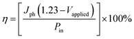
The photoconversion efficiencies (η) of ZnO NRs/CdS annealed at 500 °C and pristine ZnO NR photoanodes were calculated using eqn (9):40
| |
 | (9) |
where
Jph is the photocurrent density in (mA cm
−2),
Vapp (V) is the applied external potential and
Pin (mW cm
−2) is the power of the incident light. Here, 1.23 V is the standard reversible redox potential of water electrolysis [
vs. the normal hydrogen electrode (NHE)]. Pristine ZnO NRs arrays reached their maximum efficiency of 0.40% at 0.24 V (
vs. Ag/AgCl), while the efficiency of the annealed ZnO NRs/CdS was 4.30% at 0.28 V (
vs. Ag/AgCl), which is about 11 times higher than that of the bare ZnO NRs, indicating a stunning enhancement in the PEC performance of the ZnO NRs/CdS core–shell photoanode as depicted in
Fig. 12a.
Table 2 summarizes and compares the PEC performances of a few reported photoanodes that are similar to the present work.
 |
| | Fig. 12 Photoconversion efficiency (a) and Nyquist plots of impedance spectra (b) comparing the electrochemical properties of optimum ZnO NRs and ZnO NRs/CdS photoanodes. Schematic band energy diagram of the ZnO/CdS binary nanostructure (c) and the redox reaction occurring with the ZnO/CdS photoanode upon illumination (d). LSV polarization curve in 1 M KOH (e). | |
Table 2 A comparative study of the photoelectrochemical performance of the synthesized ZnO NRs/CdS heterostructures
| Sample |
Photoconversion efficiency |
Photocurrent density |
Ref. |
| ITO/ZnO NRs/CdS in a mixture of 0.1 M Na2S and 0.1 M Na2SO3 electrolyte |
4.39% at 0.28 V |
5.44 mA cm−2 at 0.5 V |
Current study |
| FTO/ZnO/CdS in 1 M Na2S electrolyte |
— |
5.1 mA cm−2 at 0.2 V |
18 |
| ZnO NRs/CdS in 0.5 M Na2SO4 electrolyte |
2.36% at 0.31 V |
1.75 mA cm−2 at 0 V |
34 |
| ZnO NRs/CdS in a mixture of 0.1 M Na2S and 0.1 M Na2SO3 electrolyte |
3.43% at 0 V |
2.77 mA cm−2 at 1.0 V |
40 |
| FTO/ZnO nanosheets/CdS in 0.5 M Na2SO4 electrolyte |
0.754% at 0.04 V |
2.31 mA cm−2 at 0 V |
62 |
| ITO/ZnO NRs/CdS NPs in 0.5 M Na2S electrolyte |
1.5% at −0.68 V |
4.33 mA cm−2 at 0 V |
63 |
The positive effect of thin film annealing was further investigated by electrochemical impedance measurements. An EIS spectrum provides information about electron diffusion in the mesoporous film, charge transfer resistance at the counter electrode (RPt), recombination resistance at the working electrode's interface (Rct), and electrolyte redox species diffusion, from the high to low-frequency region, successively.64 According to the EIS Nyquist plots obtained in the frequency region of 0.1–1 MHz (Fig. 12b), the charge separation efficiency and interfacial electron transfer for annealed ZnO/CdS were remarkably increased as inferred from the smaller diameter of the corresponding semicircle as compared to that of ZnO NRs. With great crystallinity, photogenerated electrons and holes can move efficiently from the photoelectrode to the electrolyte and the counter electrode, therefore, minimising the charge transfer resistance. A small number of grain boundaries also decreased the possibility of trapping site and scattering centre formation causing carrier recombination and deteriorated device performance. In this study, the charge transfer resistance and RPt for ZnO NRs were found to be 10277.9 Ω and 730.1 Ω, while for annealed CdS-sensitized ZnO NRs, the measured values were 704.3 Ω and 188.6 Ω. According to Rokade and co-workers, the smaller arc diameter of the ZnO/CdS core–shell photoanode is also proportional to a likely prolonged lifetime of photo-generated carriers, which is favourable for photovoltaic and photoelectrochemical activities. In short, increasing the annealing temperature improved the crystallinity and stability of annealed CdS thin layers (serious current leakage was inhibited), thereby leading to a reduction in electron–hole recombination in the binary photoanode. This observation is consistent with the previously reported results.30,48,65
By employing the band gap energies, the positions of the valence band (V.B.) and conduction band (C.B.) of ZnO and CdS can be estimated based on the following empirical formulas:40
| | |
EC.B. = X − 0.5Eg + E0
| (10) |
where
EC.B. and
EV.B. are conduction band and valence band potentials,
X is the electronegativity of the semiconductor with values equal to 5.79 eV and 5.18 eV for ZnO and CdS,
40 respectively,
Eg represents the bandgap energy of the semiconductor, while
E0 refers to the scaling factor describing the redox level of the reference electrode to the vacuum (
E0 = −4.5 eV for NHE). The values of
EC.B. and
EV.B. (
vs. NHE) for ZnO NRs were calculated to be −0.32 eV and 2.90 eV, while those for ZnO NRs/CdS were −0.54 eV and 1.91 eV. The schematic diagram of band gap alignment of the binary nanostructured ZnO NRs/CdS (
Fig. 12c) shows a combination of metal oxide and narrow bandgap chalcogenide sensitizer that can lead to the type-II electronic band offset with good interface quality, which in turn, guarantees a lower recombination rate in a binary semiconductor.
All the above characterization results suggest that the addition and optimization of CdS photosensitizer onto ZnO NRs arrays is beneficial for increasing the photon absorption ability and thus, the incident light-to-current conversion efficiency. A mechanism for the heterojunction formation is discussed below and the reaction at the ZnO/CdS interface is described in detail, aided by Fig. 12d. Under light irradiation with photon energy higher or equal to the bandgaps of ZnO and CdS, the electron is excited from the lower ground level (valence band, VB) to the higher level (conduction band, CB) with the simultaneous generation of the same amount of holes in the VB, leading to a large number of electron–hole pairs being present in the CdS NPs film. These photogenerated carriers could induce directional migration due to the formation of an inner electric field upon heterostructure construction. Since CdS has a higher CB potential (−0.54 V vs. NHE) than that of ZnO (−0.32 V vs. NHE), the photogenerated electrons are thermodynamically transferred from the CB of CdS to the CB of ZnO and subsequently shuttled to the ITO substrate and the Pt counter electrode through the external circuit; conversely, the photogenerated holes are transferred from the VB of ZnO to the VB of CdS. Along with this mechanism, the type-II localized charge carriers are efficiently separated in a way that the photogenerated holes localized in the valence band of CdS reach the electrode/electrolyte interface to oxidize the sacrificial species in the electrolyte while the reduction of protons on the Pt electrode produces H2. As a result, charge recombination within CdS and ZnO is diminished, followed by an enhancement in the interfacial charge transport facilitated by the dense nanorod structure together with the high electron mobility characteristic of ZnO.34,66,67 The strong hole-scavenging ability of S2− ions with the addition of SO32− ions is significant in suppressing the formation of undesirable disulfide (S22−) ions, and is thus advantageous in stabilizing CdS from photocorrosion.68
The oxidation reactions that occurred at the photoanode are as follows:68,69
| 2S2− + 2hVB+ → S22− (hole scavenging) |
| S22− + SO32− → S2O32− + S2− (suppression of disulfide formation) |
| SO32− + S2− + 2hVB+ → S2O32− |
The reduction reaction that occurred at the counter electrode is as follows:
An additional photoelectrochemical study was conducted using a typical three-electrode system in 1 M KOH (pH 14) aqueous electrolyte to investigate the electrocatalytic performance of ZnO NRs and CdS-sensitized ZnO NR photoanodes. The conversion of the recorded potential was done according to a previous report.70 In Fig. 12e, the LSV polarization curves of both pristine ZnO and ZnO/CdS samples under illumination are depicted for the oxygen evolution reaction (OER) reaction, which mainly occurs at the solid/liquid interface. Both photoanodes exhibited an anodic photocurrent that overall increased with the increasing electrode potential, similar to the PEC response observed in the Na2S/Na2SO3 medium. ZnO NRs/CdS was more active than pristine ZnO NRs as evidenced by its higher OER catalytic activity at 1.23 V (vs. RHE) in accordance with the lower overpotentials of 171 mV and 800 mV at J = 1 mA cm−2 and 10 mA cm−2, respectively. As compared to plain ZnO NRs, a smaller applied potential is required to initiate the anodic oxidative process in the ZnO/CdS photoanode under light irradiation. The better PEC–water oxidation efficiency is attributed to their lower onset potential and faster reaction kinetics,71 which can be correlated with the smaller charge transfer resistance depicted in the impedance spectra. The findings are comparable to the works of Balu et al.72
4 Conclusion
The fabrication of ZnO NRs/CdS heterostructures on ITO substrates has been demonstrated by cost-effective hydrothermal and SILAR techniques. The ZnO nanostructure sensitized with a finely dispersed thin layer of CdS nanoparticles not only allows good direct charge transport, but a larger ZnO/CdS interfacial area contributes to extensive visible-light harvesting. A PEC enhancement encouraged by a two-step preheating treatment played a significant role in interface engineering by accelerating the charge carrier transfer kinetics in solar devices. After post-annealing in a nitrogen atmosphere, the photocurrent density and photoconversion efficiency of the optimized ZnO NRs/CdS reached 5.44 mA cm−2 and 4.30%, respectively, which is 11 times higher than the bare ZnO NRs. The thickness, morphology, and crystallinity control of the CdS layer were also effective in modifying the bandwidth from 3.22 eV to 2.45 eV. These results confirmed CdS-decorated ZnO NRs as one of the promising efficient photoanodes for PEC water splitting. Future studies are required to improve the CdS film stoichiometry by varying the anionic solution concentration to subdue the issue of sulfur deficiency that might appear during the synthesis and annealing steps. It is also recommended that the effect of different applied temperatures in ZnO/CdS interface pre-treatment be investigated to obtain a more stable photoanode with higher photoconversion efficiency.
Author contributions
Conceptualization, H. J., Z. Z.; funding acquisition, Z. Z.; experiment design, H. J.; investigation, H. J. and S. T.; data analysis, H. J.; writing-original draft, H. J.; writing-review and editing, Z. Z., H. N. and N. N.; supervision, Z. Z., Z. A. and S. S. All authors have read and agreed to the published version of the manuscript.
Conflicts of interest
The authors declare no conflict of interest.
Acknowledgements
Financial support of this work via Putra grant (GP-GPB/2021/9707600) is gratefully acknowledged. Authors thank the MIMOS Berhad, Institute of Bioscience UPM, Department of Physics (Faculty of Science UPM) and Centre for Research and Instrumentation Management (CRIM), UKM for HRTEM FESEM, XRD and Raman data collection. Special thanks are extended to Yayasan Sultan Iskandar Johor on their financial support for Tan Huey Jing's PhD study.
References
- M. Mehrabian, E. N. Afshar and E. Mirzapoor, 45% efficiency enhancement of ZnO nanorod bulk-heterojunction solar cells by PbS QDs, Mater. Res. Express, 2020, 7, 5–10, DOI:10.1088/2053-1591/ab688a.
- Y. Fu, F. Cao, F. Wu, Z. Diao, J. Chen, S. Shen and L. Li, Phase-Modulated Band Alignment in CdS Nanorod/SnSx Nanosheet Hierarchical Heterojunctions toward Efficient Water Splitting, Adv. Funct. Mater., 2018, 28, 1–9, DOI:10.1002/adfm.201706785.
- C. Yang, Y. Lv, H. Zhang and X. Zhou, Double-shelled ZnO/TiO2/CdS nanorod arrays for enhanced photoelectrocatalytic performance, J. Porous Mater., 2019, 26, 903–912, DOI:10.1007/s10934-018-0686-0.
- J. Lin, Y. Liu, Y. Liu, C. Huang, W. Liu, X. Mi, D. Fan, F. Fan, H. Lu and X. Chen, SnS2 Nanosheets/H-TiO2 Nanotube Arrays as a Type II Heterojunctioned Photoanode for Photoelectrochemical Water Splitting, ChemSusChem, 2019, 12, 961–967, DOI:10.1002/cssc.201802691.
- C. Liu, F. Meng, L. Zhang, D. Zhang, S. Wei, K. Qi, J. Fan, H. Zhang and X. Cui, CuO/ZnO heterojunction nanoarrays for enhanced photoelectrochemical water oxidation, Appl. Surf. Sci., 2019, 469, 276–282, DOI:10.1016/j.apsusc.2018.11.054.
- E. Sitara, H. Nasir, A. Mumtaz, M. F. Ehsan, M. Sohail, S. Iram and S. A. B. Bukhari, Efficient photoelectrochemical water splitting by tailoring mos2/cote heterojunction in a photoelectrochemical cell, Nanomaterials, 2020, 10, 1–14, DOI:10.3390/nano10122341.
- S. Velanganni, S. Pravinraj, P. Immanuel and R. Thiruneelakandan, Nanostructure CdS/ZnO heterojunction configuration for photocatalytic degradation of Methylene blue, Phys. Rev. B: Condens. Matter Mater. Phys., 2018, 534, 56–62, DOI:10.1016/j.physb.2018.01.027.
- A. C. Mendhe, S. Majumder, S. M. Pawar and B. R. Sankapal, Facile Bi2S3 nanoparticles on CdS nanowires surface: core-shell nanostructured design towards solar cell application, Surf. Interfaces, 2021, 27, 101457, DOI:10.1016/j.surfin.2021.101457.
- V. Consonni, S. Renet, J. Garnier, P. Gergaud, L. Artús, J. Michallon, L. Rapenne, E. Appert and A. Kaminski-Cachopo, Improvement of the physical properties of ZnO/CdTe core-shell nanowire arrays by CdCl2 heat treatment for solar cells, Nanoscale Res. Lett., 2014, 9, 1–13, DOI:10.1186/1556-276X-9-222.
- X. Yin, W. Que, D. Fei, H. Xie, Z. He and G. Wang, Strategies to prepare an efficient photoanode for ZnO nanowires-based CdS-CdSe co-sensitized solar cells, Electrochim. Acta, 2013, 89, 561–570, DOI:10.1016/j.electacta.2012.11.016.
- Y. Tak, S. J. Hong, J. S. Lee and K. Yong, Solution-based synthesis of a cds nanoparticle/zno nanowire heterostructure array, Cryst. Growth Des., 2009, 9, 2627–2632, DOI:10.1021/cg801076b.
- A. Pareek and P. H. Borse, Hurdles and recent developments for CdS and chalcogenide-based electrode in “Solar electro catalytic” hydrogen generation: a review, Electrochem. Sci. Adv., 2021, 1–25, DOI:10.1002/elsa.202100114.
- X. Bai, F. Purcell-Milton and Y. K. Gun’ko, Optical properties, synthesis, and potential applications of cu-based ternary or quaternary anisotropic quantum dots, polytypic nanocrystals, and core/shell heterostructures, Nanomaterials, 2019, 9(1), 85, DOI:10.3390/nano9010085.
- S. Horoz, Synthesis of W(3%)-doped CdS thin film by SILAR and its characterization, J. Mater. Sci.: Mater. Electron., 2018, 29, 7519–7525, DOI:10.1007/s10854-018-8743-7.
- R. K. Choubey, D. Desai, S. N. Kale and S. Kumar, Effect of annealing treatment and deposition temperature on CdS thin films for CIGS solar cells applications, J. Mater. Sci.: Mater. Electron., 2016, 27, 7890–7898, DOI:10.1007/s10854-016-4780-2.
- Z. Bai and Y. Zhang, A Cu2O/Cu2S-ZnO/CdS tandem photoelectrochemical cell for self-driven solar water splitting, J. Alloys Compd., 2017, 698, 133–140, DOI:10.1016/j.jallcom.2016.12.261.
- Z. K. Heiba, M. B. Mohamed and N. G. Imam, Biphasic quantum dots of cubic and hexagonal Mn doped CdS: necessity of rietveld analysis, J. Alloys Compd., 2015, 618, 280–286, DOI:10.1016/j.jallcom.2014.08.106.
- H. Nan, W. Wu, K. Feng, B. Shan, Y. Qiu and Y. Zhang, Improved photocatalytic efficiency and stability of CdS/ZnO shell/core nanoarrays with high coverage and enhanced interface combination, Int. J. Hydrogen Energy, 2017, 42, 848–857, DOI:10.1016/j.ijhydene.2016.10.135.
- X. Ning and G. Lu, Photocorrosion inhibition of CdS-based catalysts for photocatalytic overall water splitting, Nanoscale, 2020, 12, 1213–1223, 10.1039/c9nr09183a.
- B. Duan, L. Lou, F. Meng, J. Zhou, J. Wang, J. Shi, H. Wu, Y. Luo, D. Li and Q. Meng, Two-Step Annealing CZTSSe/CdS Heterojunction to Improve Interface Properties of Kesterite Solar Cells, ACS Appl. Mater. Interfaces, 2021, 13, 55243–55253, DOI:10.1021/acsami.1c18152.
- W. C. Chen, C. H. C. Y. Chen, Y. R. Lin, J. K. Chang, C. H. C. Y. Chen, Y. P. Chiu, C. I. Wu, K. H. Chen and L. C. Chen, Interface engineering of CdS/CZTSSe heterojunctions for enhancing the Cu2ZnSn(S,Se)4 solar cell efficiency, Mater. Today Energy, 2019, 13, 256–266, DOI:10.1016/j.mtener.2019.05.015.
- H. J. Tan, Z. Zainal, Z. A. Talib, H. N. Lim, S. Shafie, S. T. Tan, K. B. Tan and N. N. Bahrudin, Synthesis of high quality hydrothermally grown ZnO nanorods for photoelectrochemical cell electrode, Ceram. Int., 2021, 47, 14194–14207, DOI:10.1016/j.ceramint.2021.02.005.
- C. Rosiles-perez, A. Cerdán-Pasarán, S. Sidhik, D. Esparza, T. López-Luke, E. de la Rosa, E. De Rosa, E. de la Rosa and E. De Rosa, Improved performance of CdS quantum dot sensitized solar cell by solvent modi fi ed SILAR approach, Sol. Energy, 2018, 174, 240–247, DOI:10.1016/j.solener.2018.08.081.
- L. Arunraja, P. Thirumoorthy, A. Karthik, R. Subramanian and V. Rajendran, Investigation and characterization of ZnO/CdS nanocomposites using chemical precipitation method for gas sensing applications, J. Mater. Sci.: Mater. Electron., 2017, 28, 18113–18120, DOI:10.1007/s10854-017-7756-y.
- Q. Nie, L. Yang, C. Cao, Y. Zeng, G. Wang, C. Wang and S. Lin, Interface optimization of ZnO nanorod/CdS quantum dots heterostructure by a facile two-step low-temperature thermal treatment for improved photoelectrochemical water splitting, Chem. Eng. J., 2017, 325, 151–159, DOI:10.1016/j.cej.2017.05.021.
- V. D. Moreno-Regino, F. M. Castañeda-de-la-Hoya, C. G. Torres-Castanedo, J. Márquez-Marín, R. Castanedo-Pérez, G. Torres-Delgado and O. Zelaya-Ángel, Structural, optical, electrical and morphological properties of CdS films deposited by CBD varying the complexing agent concentration, Results Phys., 2019, 13, 102238, DOI:10.1016/j.rinp.2019.102238.
- K. Ravichandran, N. Nisha Banu, V. Senthamil Selvi, B. Muralidharan and T. Arun, Rectification of sulphur deficiency defect in CdS based films by introducing a novel modification in the SILAR cyclic process, J. Alloys Compd., 2016, 687, 402–412, DOI:10.1016/j.jallcom.2016.06.164.
- H. M. Pathan and C. D. Lokhande, Deposition of metal chalcogenide thin films by successive ionic layer adsorption and reaction (SILAR) method, Bull. Mater. Sci., 2004, 27, 85–111, DOI:10.1007/BF02708491.
- S. Y. Lee, J. Y. Oh, R. P. Patil, M. Kim, J. S. Jang, H. Jin, S. Kim and H. J. Lee, A general guide for adsorption of cadmium sulfide (CdS) quantum dots by successive ionic layer adsorption and reaction (SILAR) for efficient CdS-sensitized photoelectrochemical cells, Appl. Surf. Sci., 2022, 589, 152898, DOI:10.1016/j.apsusc.2022.152898.
- B. R. Sankapal, D. B. Salunkhe, S. Majumder and D. P. Dubal, Solution-processed CdS quantum dots on TiO2: light-induced electrochemical properties, RSC Adv., 2016, 6, 83175–83184, 10.1039/c6ra14275c.
- L. Al-Gebory and M. P. Mengüç, The effect of pH on particle agglomeration and optical properties of nanoparticle suspensions, J. Quant. Spectrosc. Radiat. Transfer, 2018, 219, 46–60, DOI:10.1016/j.jqsrt.2018.07.020.
- M. Saxena, T. Patel, V. Sharma and G. S. Okram, Synthesis and dispersion medium-dependent stability of cadmium sulfide nanoparticles, AIP Conf. Proc., 2019, 2162, 1–5, DOI:10.1063/1.5130300.
- G. Yuvaraja, C. Prasad, Y. Vijaya and M. V. Subbaiah, Application of ZnO nanorods as an adsorbent material for the removal of As(III) from aqueous solution: kinetics, isotherms and thermodynamic studies, Int. J. Ind. Chem., 2018, 9, 17–25, DOI:10.1007/s40090-018-0136-5.
- I. Biswas, P. Roy, P. K. Sinha, M. Kanu and A. K. Chakraborty, Activating ZnO nanorods photoanodes in visible light by CdS surface sensitiser, Micro Nano Lett., 2019, 14, 941–946, DOI:10.1049/mnl.2018.5700.
- S. U. Shaikh, D. J. Desale, F. Y. Siddiqui, A. Ghosh, R. B. Birajadar, A. V. Ghule and R. Sharma, Effects of air annealing on CdS quantum dots thin film grown at room temperature by CBD technique intended for photosensor applications, Mater. Res. Bull., 2012, 47, 3440–3444, DOI:10.1016/j.materresbull.2012.07.009.
- H. A. Colorado, S. R. Dhage and H. T. Hahn, Thermo chemical stability of cadmium sulfide nanoparticles under intense pulsed light irradiation and high temperatures, Mater. Sci. Eng., B, 2011, 176, 1161–1168, DOI:10.1016/j.mseb.2011.06.003.
- V. N. Volodin, Y. Z. Tuleushev, B. K. Kenzhaliyev and S. A. Trebukhov, Thermal degradation of hard alloys of the niobiumcadmium system at low pressure, Kompleksnoe Ispolʹzovanie Mineralʹnogo syrʹâ, 2020, 312, 41–47, DOI:10.31643/2020/6445.05.
- S. S. Hegde, P. Murahari, B. J. Fernandes, R. Venkatesh and K. Ramesh, Synthesis, thermal stability and structural transition of cubic SnS nanoparticles, J. Alloys Compd., 2020, 820, 153116, DOI:10.1016/j.jallcom.2019.153116.
- W. Yang, W. Wu, W. Chen, J. Zhao and X. Hu, Structural modulation of CdS/ZnO nanoheterojunction arrays for full solar water splitting and their related degradation mechanisms, Catal. Sci. Technol., 2018, 8, 5280–5287, 10.1039/c8cy01549j.
- A. M. Holi, Z. Zainal, Z. A. Talib, H. N. Lim, C. C. Yap, S. K. Chang and A. K. Ayal, Enhanced photoelectrochemical performance of ZnO nanorod arrays decorated with CdS shell and Ag2S quantum dots, Superlattices Microstruct., 2017, 103, 295–303, DOI:10.1016/j.spmi.2017.01.035.
- M. A. Zubair, M. T. Chowdhury, M. S. Bashar, M. A. Sami and M. F. Islam, Thickness dependent correlation between structural and optical properties of textured CdSe thin film, AIP Adv., 2019, 9(4), 45123, DOI:10.1063/1.5096594.
- J. P. Enríquez, Effect of annealing time and temperature on structural, optical and electrical properties of cds films deposited by cbd, Chalcogenide Lett., 2013, 10, 45–53 Search PubMed.
- O. K. Echendu, F. B. Dejene, I. M. Dharmadasa and F. C. Eze, Characteristics of Nanocrystallite-CdS Produced by Low-Cost Electrochemical Technique for Thin Film Photovoltaic Application: The Influence of Deposition Voltage, Int. J. Photoenergy, 2017, 2017, 3989432, DOI:10.1155/2017/3989432.
- R. Keshav, A. Rao and M. G. Mahesha, Raman spectroscopy and low temperature electrical conductivity study of thermally evaporated CdS thin films, Opt. Quantum Electron., 2018, 50, 1–14, DOI:10.1007/s11082-018-1451-y.
- A. Kamble, B. Sinha, G. Agawane, S. Vanalakar, I. Y. Kim, J. Y. Kim, S. S. Kale, P. Patil and J. H. Kim, Sulfur ion concentration dependent morphological evolution of CdS thin films and its subsequent effect on photo-electrochemical performance, Phys. Chem. Chem. Phys., 2016, 18, 28024–28032, 10.1039/c6cp00903d.
- A. Hassanpour, N. Bogdan, J. A. Capobianco and P. Bianucci, Hydrothermal selective growth of low aspect ratio isolated ZnO nanorods, Mater. Des., 2017, 119, 464–469, DOI:10.1016/j.matdes.2017.01.089.
- A. V. Kozytskiy, O. L. Stroyuk, S. Y. Kuchmiy, A. V. Mazanik, S. K. Poznyak, E. A. Streltsov, A. I. Kulak, O. V. Korolik and V. M. Dzhagan, Photoelectrochemical and Raman characterization of nanocrystalline CdS grown on ZnO by successive ionic layer adsorption and reaction method, Thin Solid Films, 2014, 562, 56–62, DOI:10.1016/j.tsf.2014.03.070.
- A. Rokade, S. Rondiya, A. Date, V. Sharma, M. Prasad, H. Pathan and S. Jadkar, Electrochemical Synthesis of Core-shell ZnO/CdS Nanostructure for Photocatalytic Water Splitting Application, Energy Procedia, 2017, 110, 121–127, DOI:10.1016/j.egypro.2017.03.116.
- J. Jiang, M. Wang, L. Ma, Q. Chen and L. Guo, Synthesis of uniform ZnO/ZnS/CdS nanorod films with ion-exchange approach and photoelectrochemical performances, Int. J. Hydrogen Energy, 2013, 38, 13077–13083, DOI:10.1016/j.ijhydene.2013.03.056.
- W. Yang, R. R. Prabhakar, J. Tan, S. D. Tilley and J. Moon, Strategies for enhancing the photocurrent, photovoltage, and stability of photoelectrodes for photoelectrochemical water splitting, Chem. Soc. Rev., 2019, 48, 4979–5015, 10.1039/c8cs00997j.
- M. F. Mohamad Noh, M. F. Soh, M. A. Riza, J. Safaei, S. N. F. Mohd Nasir, N. W. Mohamad Sapian, C. H. Teh, M. A. Ibrahim, N. Ahmad Ludin and M. A. Mat Teridi, Effect of Film Thickness on Photoelectrochemical Performance of SnO2 Prepared via AACVD, Phys. Status Solidi B, 2018, 255(6), 1700570, DOI:10.1002/pssb.201700570.
- J. Y. Cho, S. Sinha, M. G. Gang and J. Heo, Controlled thickness of a chemical-bath-deposited CdS buffer layer for a SnS thin film solar cell with more than 3% efficiency, J. Alloys Compd., 2019, 796, 160–166, DOI:10.1016/j.jallcom.2019.05.035.
- S. Verma and H. N. Ghosh, Carrier relaxation dynamics in type-II ZnO/CdSe quantum dot heterostructures, Phys. Chem. Chem. Phys., 2017, 19, 24896–24902, 10.1039/c7cp04069e.
- S. K. Kokate, A. T. Supekar, P. K. Baviskar, B. M. Palve, S. R. Jadkar, K. C. Mohite and H. M. Pathan, CdS sensitized pristine and Cd doped ZnO solar cells: effect of SILAR cycles on optical properties and efficiency, Mater. Sci. Semicond. Process., 2018, 80, 179–183, DOI:10.1016/j.mssp.2018.02.033.
- M. Dongol, A. El-Denglawey, M. S. Abd El Sadek and I. S. Yahia, Thermal annealing effect on the structural and the optical properties of Nano CdTe films, Optik, 2015, 126, 1352–1357, DOI:10.1016/j.ijleo.2015.04.048.
- I. M. S. Mohammed, G. M. M. Gubari, N. P. Huse, A. S. Dive, S. H. Han and R. Sharma, Effect of Cd/S ratio on growth and physical properties of CdS thin films for photosensor application, J. Mater. Sci.: Mater. Electron., 2020, 31, 9989–9996, DOI:10.1007/s10854-020-03543-z.
- M. S. Bashar, R. Matin, M. Sultana, A. Siddika, M. Rahaman, M. A. Gafur and F. Ahmed, Effect of rapid thermal annealing on structural and optical properties of ZnS thin films fabricated by RF magnetron sputtering technique, J. Theor. Appl. Phys., 2020, 14, 53–63, DOI:10.1007/s40094-019-00361-5.
- J. Xiao, L. Peng, L. Gao, J. Zhong, Z. Huang, E. Yuan, V. Srinivasapriyan, S. F. Zhou and G. Zhan, Improving light absorption and photoelectrochemical performance of thin-film photoelectrode with a reflective substrate, RSC Adv., 2021, 11, 16600–16607, 10.1039/d1ra02826j.
- E. E. El-Katori, M. A. Ahmed, A. A. El-Bindary and A. M. Oraby, Impact of CdS/SnO2 heterostructured nanoparticle as visible light active photocatalyst for the removal methylene blue dye, J. Photochem. Photobiol., A, 2020, 392, 112403, DOI:10.1016/j.jphotochem.2020.112403.
- P. R. Nikam, P. K. Baviskar, S. Majumder, J. V. Sali and B. R. Sankapal, SILAR controlled CdSe nanoparticles sensitized ZnO nanorods photoanode for solar cell application: electrolyte effect, J. Colloid Interface Sci., 2018, 524, 148–155, DOI:10.1016/j.jcis.2018.03.111.
- L. Yang, Z. Zhang, J. Yang, Y. Yan, Y. Sun, G. Che, Z. Wang and S. Zhang, Enhancement mechanism of photovoltaic performance for ZnO/CdS heterostructure photoelectrodes via post-annealing treatment, Superlattices Microstruct., 2013, 60, 426–436, DOI:10.1016/j.spmi.2013.05.025.
- C. Mahala, M. D. Sharma and M. Basu, ZnO@CdS heterostructures: an efficient photoanode for photoelectrochemical water splitting, New J. Chem., 2019, 43, 7001–7010, 10.1039/c9nj01373c.
- N. M. Vuong, T. T. Hien, N. D. Quang, N. D. Chinh, D. S. Lee, D. Kim and D. Kim, H2- and NH3-treated ZnO nanorods sensitized with CdS for photoanode enhanced in photoelectrochemical performance, J. Power Sources, 2016, 317, 169–176, DOI:10.1016/j.jpowsour.2016.03.106.
- X. Qiu, L. Chen, H. Gong, M. Zhu, J. Han, M. Zi, X. Yang, C. Ji and B. Cao, The influence of annealing temperature on the interface and photovoltaic properties of CdS/CdSe quantum dots sensitized ZnO nanorods solar cells, J. Colloid Interface Sci., 2014, 430, 200–206, DOI:10.1016/j.jcis.2014.05.057.
- S. Cao, X. Yan, Z. Kang, Q. Liang, X. Liao and Y. Zhang, Band alignment engineering for improved performance and stability of ZnFe2O4modified CdS/ZnO nanostructured photoanode for PEC water splitting, Nano Energy, 2016, 24, 25–31, DOI:10.1016/j.nanoen.2016.04.001.
- X. An and Y. Zhang, Fabrication of NiO quantum dot-modified ZnO nanorod arrays for efficient photoelectrochemical water splitting, Appl. Phys. A: Mater. Sci. Process., 2017, 123, 1–6, DOI:10.1007/s00339-017-1237-2.
- Y. Tang, P. Traveerungroj, H. L. Tan, P. Wang, R. Amal and Y. H. Ng, Scaffolding an ultrathin CdS layer on a ZnO nanorod array using pulsed electrodeposition for improved photocharge transport under visible light illumination, J. Mater. Chem. A, 2015, 3, 19582–19587, 10.1039/c5ta05195a.
- C. Ng, J. H. Yun, H. L. Tan, H. Wu, R. Amal and Y. H. Ng, A dual-electrolyte system for photoelectrochemical hydrogen generation using CuInS2-In2O3-TiO2 nanotube array thin film, Sci. China Mater., 2018, 61, 895–904, DOI:10.1007/s40843-017-9237-2.
- A. M. Huerta-Flores, L. M. Torres-Martínez, E. Moctezuma, A. P. Singh and B. Wickman, Green synthesis of earth-abundant metal sulfides (FeS2, CuS, and NiS2) and their use as visible-light active photocatalysts for H2 generation and dye removal, J. Mater. Sci.: Mater. Electron., 2018, 29, 11613–11626, DOI:10.1007/s10854-018-9259-x.
- C. Sathiskumar, S. Ramakrishnan, M. Vinothkannan, A. R. Kim, S. Karthikeyan and D. J. Yoo, Nitrogen-doped porous carbon derived from biomass used as trifunctional electrocatalyst toward oxygen reduction, oxygen evolution and hydrogen evolution reactions, Nanomaterials, 2020, 10, 1–17, DOI:10.3390/nano10010076.
- T. Higashi, H. Nishiyama, V. Nandal, Y. Pihosh, Y. Kawase, R. Shoji, M. Nakabayashi, Y. Sasaki, N. Shibata, H. Matsuzaki, K. Seki, K. Takanabe and K. Domen, Design of semitransparent tantalum nitride photoanode for efficient and durable
solar water splitting, Energy Environ. Sci., 2022, 15, 4761–4775, 10.1039/d2ee02090d.
- S. Balu, H. Venkatesvaran and K. Lan, Synthesis of Highly Efficient (0D/1D) Z-Scheme CdS-NPs@ZnO-NRs Visible-Light-Driven Photo(electro)catalyst for PEC Oxygen Evolution Reaction and Removal of Tetracycline, Catalyst, 2022, 12, 1–19 Search PubMed.
|
| This journal is © The Royal Society of Chemistry 2023 |
Click here to see how this site uses Cookies. View our privacy policy here. 
 Open Access Article
 This Open Access Article is licensed under a Creative Commons Attribution-Non Commercial 3.0 Unported Licence
 a,
Zulkarnain Zainal*ac,
Zainal Abidin Talibb,
Hong Ngee Lim
a,
Zulkarnain Zainal*ac,
Zainal Abidin Talibb,
Hong Ngee Lim