
 Open Access Article
 This Open Access Article is licensed under a Creative Commons Attribution-Non Commercial 3.0 Unported Licence
Photocatalysis screening for group III–V vdW heterostructures constructed by MX (M = Ga, In and X = P, As) monolayers†
Yingjie Chena,
Baonan Jia *ab,
Guoying Qina,
Huiyan Zhaoa,
Lihong Hana and
Pengfei Lu*ac
*ab,
Guoying Qina,
Huiyan Zhaoa,
Lihong Hana and
Pengfei Lu*ac
aState Key Laboratory of Information Photonics and Optical Communications, Beijing University of Posts and Telecommunications, Beijing 100876, China. E-mail: jiabaonan@163.com; photon.bupt@gmail.com
bSchool of Electronic Engineering, Beijing University of Posts and Telecommunications, Beijing 100876, China
cSchool of Integrated Circuits, Beijing University of Posts and Telecommunications, Beijing 100876, China
First published on 16th May 2023
Abstract
To harvest solar energy for water splitting and produce pollution-free hydrogen and oxygen, high-performance photocatalysts are essential. Here, by combining different two-dimensional (2D) group III–V MX (M = Ga, In and X = P, As) monolayers, we designed 144 van der Waals (vdW) heterostructures to identify efficient photoelectrochemical materials. Using first-principles calculations, we investigated the stabilities, electronic properties, and optical properties of these heterostructures. After a careful screening process, we elected GaP/InP in a BB-II stacking configuration as the most promising candidate. This specific GaP/InP configuration has a type-II band alignment with a gap value of 1.83 eV. The conduction band minimum (CBM) is located at −4.276 eV, and the valence band maximum (VBM) is located at −6.217 eV, fully satisfying the requirements of the catalytic reaction under pH = 0. Additionally, light absorption has been improved through the construction of the vdW heterostructure. These results could help in understanding the properties of the III–V heterostructures and guide the experimental synthesis of these materials for photocatalysis applications.
I. Introduction
The ability to produce pollution-free energy has made high-efficiency photocatalysts for solar water splitting an area of great interest over the past few decades.1–3 Among all the materials systems considered for photocatalysis applications, group III–V semiconductors with outstanding electronic and optical properties are particularly promising for solar-driven photoelectrochemical water-splitting, such as GaN, GaAs, and GaInP.4–7 To proceed with a catalytic reaction, the valence band maximum (VBM) of the photocatalysts must be lower than the water oxidation (H2O/O2) potential, while the conduction band minimum (CBM) should be higher than the hydrogen reduction (H+/H2) potential.8 However, the practical utilization of these III–V materials has been limited due to their large band gap, which may significantly lower the efficiency of the water-splitting process.9,10 In such cases, it is urgent to develop and optimize new prospective semiconductor photocatalysts.The discovery of the van der Waals (vdW) heterostructure has shed some light on the design of efficient photocatalysts.11 These heterostructures are formed by combining two different monolayers via van der Waals interactions vertically.12 Particularly, they can have a type-II band alignment with the conduction band minimum (CBM) and valence band maximum (VBM) located in different layers. This is beneficial for solar energy-related areas, as it allows for the separation of the photogenerated holes and electrons, which can extend the lifetime of these carriers.13,14 Additionally, constructing vdW heterostructures can adjust the band gap to a proper value, promoting photo energy harvesting.15
In this study, we designed a series of 2D group III–V van der Waals (vdW) heterostructures from MX (M = Ga, In, and X = P, As) monolayers. For each of these heterostructures, we considered multiple configurations. To identify potential candidates for water-splitting photocatalysts, we conducted a systematic screening process. First, we confirmed the stability of these configurations. Second, we analyzed the electronic properties of the different configurations. Finally, we calculated the detailed optical properties of the most promising candidates. This research not only enhances our understanding of the properties and applications of group III–V heterostructures but also provides insight into exploring new and efficient materials for photocatalytic water-splitting.
II. Computational details
The structural, electronic, and optical properties were investigated using first-principles calculations based on density functional theory (DFT) methods, as implemented in the Vienna Ab initio Simulation Package (VASP).16–18 The core–electron interaction was generated using the projector augmented-wave (PAW) method.19 The exchange–correlation interactions were described by the generalized gradient approximation (GGA) parametrized by the Perdew, Burke, and Ernzerhof (PBE).20 For the band structure calculation, the hybrid functional of Heyd, Scuseria, and Ernzerhof (HSE06) was added.20,21 An out-of-plain lattice parameter of 20 Å was set for all the 2D structures. After careful iteration testing, 1 × 10⁻⁵ eV for energies and 0.05 eV Å−1 for the forces were proved to be converged. A cutoff energy of 450 eV was set and a Γ-centered grid of 8 × 8 × 1 was used for the Brillouin zone.22 Since the influence of the vdW interaction is strong on these vdW heterostructures, the DFT-D3 method with Becke–Johnson damping was taken for the systems.23 For the accurate HSE06 method, a fraction of 0.3 for the exact exchange and a screening parameter of 0.2 Å−1 were employed.24 Since the d electrons of gallium and indium elements had little influence on the properties investigated, they were considered as core states.For the screening of photocatalysts, a total of 144 structures were constructed by combining the four 2D materials and changing the relative positions of the interfaces. We started by investigating their energetic stabilization using the formation energy and interface binding energy as the first descriptors. We found that 130 structures had negative formation energies and were energetically favorable. Since the bandgap of the photocatalyst must be greater than 1.23 eV for the water-splitting process,8 we used electronic properties as the second descriptor. Based on the band structures of the 130 candidates, we identified 36 configurations that were promising for photocatalytic applications. For the hydrogen evolution and oxygen evolution reactions to take place under pH = 0 conditions, we applied the third descriptor, which required the conduction band minimum (CBM) to be greater than −4.44 eV and the valence band maximum (VBM) to be lower than −5.67 eV. We aligned the band levels of the 36 configurations according to the vacuum level, and found that 11 configurations satisfied this requirement. Finally, we investigated the light absorption properties of the 5 type-II heterostructures that showed promising photocatalytic properties. The overall screening process is illustrated in Fig. 1.
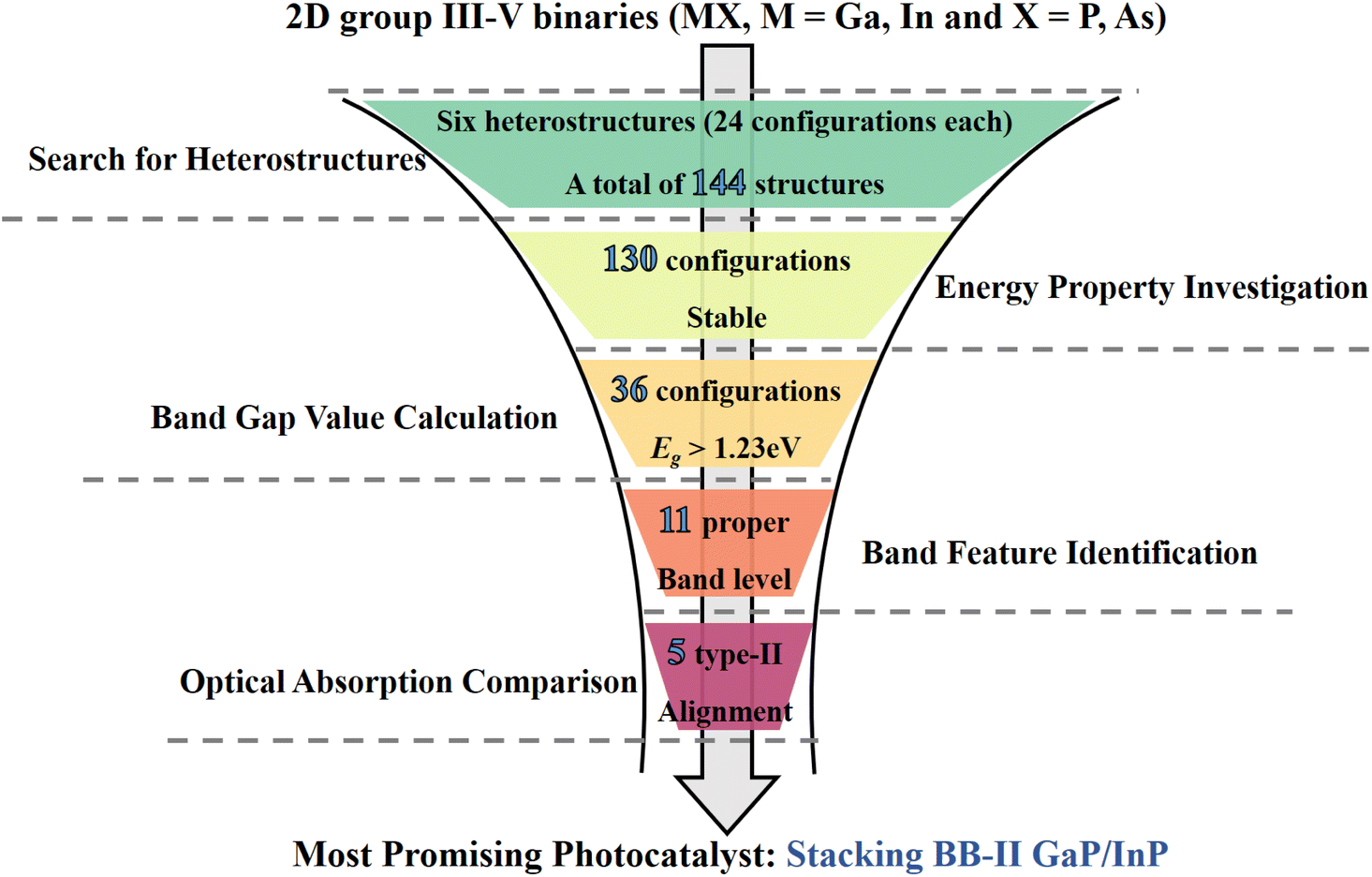 | ||
| Fig. 1 Schematic for the down-selection of potential van der Waals heterostructure photocatalysts using first-principles calculations. | ||
III. Results and discussion
The 2D group III–V (MX, M = Ga, In and X = P, As) monolayers all have bulk hexagonal structures, and the optimized lattice parameters for GaP, GaAs, InP, and InAs are 3.92, 4.06, 4.25, and 4.38 Å, respectively, which agree well with previous studies.25–27 Fig. S1† illustrates the band structures of these monolayers, with bandgap values of 2.95 eV, 1.84 eV, 1.99 eV, and 1.43 eV for GaP, GaAs, InP, and InAs, respectively. Since these values exceed 1.23 eV, these monolayers are found unsuitable for water-splitting reactions. However, Fig. S2† shows that these group III–V monolayers are highly effective in absorbing solar energy. By forming heterostructures, the band properties of these materials can be modified to create suitable photocatalysts. With lattice mismatches within an acceptable range and similar geometric properties, the construction of vertical vdW heterostructures should be stable. There are six different combinations with these 4 monolayers (GaP/GaAs, GaP/InP, GaP/InAs, GaAs/InP, GaAs/InAs, and InP/InAs). The constant difference between the constructed heterostructures and the monolayers is shown in Table S1.† For each combination of the M1X1/M2X2 heterostructures (with M1X1 as the top layer and M2X2 as the bottom layer), 24 possible stacking configurations can be achieved by changing the relative position and symmetrically flipping the two monolayers, as shown in Fig. 2. Fig. 2(a)–(d) present the side views of four different stacking models which are labeled as stacking-AA, stacking-AB, stacking-BA, and stacking-BB. The main differences are the atoms at the interface. In the stacking-AA structure, the top layer M1X1 is stacked on the bottom layer M2X2 with the same orientation, leaving the interface atoms consisting of M1 atoms and X2 atoms. The stacking-AB, stacking-BA, and stacking-BB can be obtained by a 180° vertically mirror flipping of the M2X2 layer, M1X1 layer, and both the two layers, of the stacking-AA configuration, respectively. The interface atoms will change accordingly, being consisted of M1 atoms/M2 atoms, X1 atoms/X2 atoms, and X1 atoms/M2 atoms for stacking-AB, stacking-BA and stacking-BB, respectively. Different compositions of the contact interface should lead to unique properties. For each of these four stacking models, six different configurations that can be constructed, as shown in Fig. 2(e)–(j). From the top and side views, it can be seen that in structure-I the M1 and X1 atoms are directly above M2 and X2 atoms, respectively. Structure-II and -III can be obtained by moving the top layer M1X1 of structure-I along the [110] direction with 1/3 and 2/3 a, respectively. The transition from structure-I to structure-IV is the rotation of the M1X1 along the z-axis with an angle of 180°. Moreover, structures-V and -VI can be obtained in the same way as structures-II and -III, by shifting the M1X1 layer of structure-IV along the [110] direction with 1/3 and 2/3 a, respectively. Thus, 24 different configurations can be obtained for each heterostructure, and since there are six heterostructures, a total of 144 structures were constructed.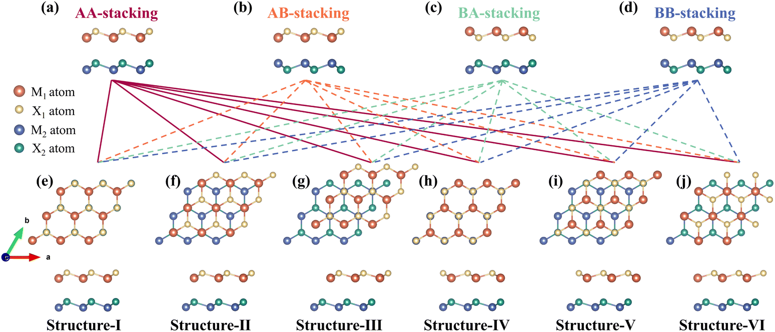 | ||
| Fig. 2 (a)–(d) The side views of 4 different stacking models for the M1X1/M2X2 heterostructure. (e)–(j) The top and side views of the 6 possible structures of each stacking model with AA-stacking as an example. A total of 144 different configurations are achieved (with 24 configurations for each M1X1/M2X2 heterostructure). | ||
The formation energy Ef is an important parameter to characterize the stability of the heterostructure, which could be calculated by the following equation:
| Ef = Etot(M1X1/M2X2) − Etot(M1X1) − Etot(M2X2) | (1) |
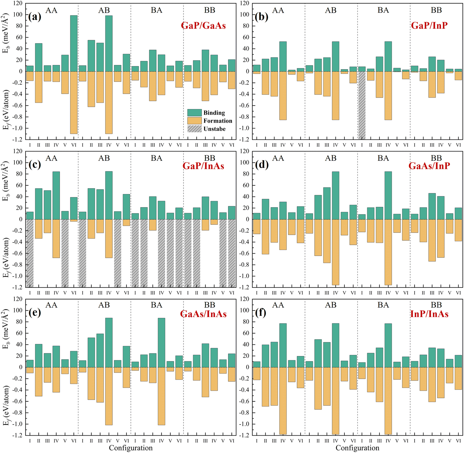 | ||
| Fig. 3 The formation energies Ef (eV per atom) (yellow bars) and the binding energies Eb (meV Å−2) (green bars) for the configurations of (a) GaP/GaAs, (b) GaP/InP, (c) GaP/InAs, (d) GaAs/InP, (e) GaAs/InAs, and (f) InP/InAs heterostructures. The structures with positive formation energies are considered unstable and marked with grey bars. | ||
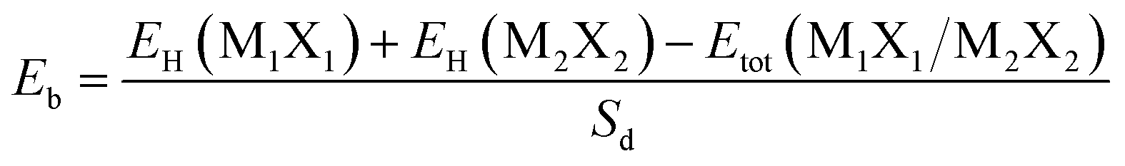
To further assess the vdW interaction force between the M1X1 and M2X2 layers, we calculated the interfacial binding energy Eb of these configurations, which could be defined by:
 | (2) |
The electronic structures are the key parameters to predict the performance of the photocatalysts. To further screen these configurations, we calculated the band structure properties of these heterostructures. The calculated results are shown in Table 1. As is known, the bandgaps for a photocatalyst must be larger than 1.23 eV. Therefore, we used the PBE method to calculate the bandgaps as a preliminary screening to eliminate those configurations with too small bandgaps. We found that most of the heterostructures are semiconductors or semi-metals with bandgaps distributed in the range of 0–1.5 eV for GaP/GaAs, GaP/InP, GaAs/InP, and InP/InAs. For GaP/InAs and GaAs/InAs, excluding the unstable configurations, most of the remaining ones are metals. Comparing different stacking models, stacking-BB holds the largest bandgaps on average for all six groups of heterostructures. However, the PBE method is known to underestimate the bandgaps for semiconductors,30 so configurations with PBE bandgaps greater than 0.6 eV were further investigated using the HSE06 method. The calculated results are shown in Table 1. Eliminated configurations are marked with a short dash. It was found that 34 configurations met the requirement of 1.23 eV. Most configurations of GaP/GaAs can meet this requirement, as well as several GaP/InP and GaAs/InP configurations. However, only a few GaP/InAs, GaAs/InAs, and InP/InAs configurations were found to be acceptable, which indicates that InAs may not be suitable for constructing photocatalysts with other group III–V materials. Especially, most qualified configurations were in stacking-BB, indicating that stacking-BB is a more promising construction of structure for photocatalysis than the other three stacking models.
| Gap (eV) | GaP/GaAs | GaP/InP | GaP/InAs | GaAs/InP | GaAs/InAs | InP/InAs | ||||||
|---|---|---|---|---|---|---|---|---|---|---|---|---|
| Eg PBE | Eg HSE | Eg PBE | Eg HSE | Eg PBE | Eg HSE | Eg PBE | Eg HSE | Eg PBE | Eg HSE | Eg PBE | Eg HSE | |
| AA-I | 0.35 | — | Metal | — | Unstable | 0.00 | — | Metal | — | 0.00 | — | |
| AA-II | 0.92 | 1.63 | Metal | — | Metal | — | Metal | — | Metal | — | Metal | — |
| AA-III | 1.02 | 1.74 | 0.99 | 1.69 | 0.33 | — | 0.21 | — | Metal | — | 0.83 | 1.49 |
| AA-IV | 0.98 | 1.98 | Metal | — | Metal | — | Metal | — | Metal | — | 0.00 | — |
| AA-V | 0.57 | — | Metal | — | Unstable | 0.05 | — | Metal | — | 0.01 | — | |
| AA-VI | 0.02 | — | 0.02 | — | Metal | — | 0.15 | — | 0.01 | — | 0.15 | — |
| AB-I | 1.02 | 1.75 | 0.00 | — | Unstable | 0.29 | — | Metal | — | 0.56 | — | |
| AB-II | 0.02 | — | Metal | — | Metal | — | Metal | — | Metal | — | Metal | — |
| AB-III | 0.89 | 1.52 | 1.00 | 1.71 | 0.35 | — | 0.80 | 1.42 | 0.61 | 1.22 | 0.85 | 1.50 |
| AB-IV | Metal | — | 0.00 | — | Metal | — | 0.00 | — | Metal | — | 0.00 | — |
| AB-V | 1.01 | 1.98 | 0.00 | — | Unstable | 0.38 | — | Metal | — | 0.56 | — | |
| AB-VI | 0.31 | — | 0.08 | — | Metal | — | 0.31 | — | Metal | — | 0.44 | — |
| BA-I | 0.98 | 1.83 | Unstable | Unstable | 0.73 | 1.20 | 0.00 | — | 0.40 | — | ||
| BA-II | 0.98 | 2.04 | 0.35 | — | Unstable | 0.59 | — | 0.00 | — | Metal | — | |
| BA-III | 1.16 | 1.23 | 0.91 | 1.25 | 0.67 | 1.26 | 0.34 | — | Metal | — | 0.70 | 1.07 |
| BA-IV | 0.65 | 1.12 | 0.00 | — | Unstable | 0.00 | — | Metal | — | 0.01 | — | |
| BA-V | 0.95 | 1.80 | 0.38 | — | Unstable | 0.74 | 1.20 | 0.00 | — | 0.41 | — | |
| BA-VI | 0.86 | 1.84 | 0.37 | — | Unstable | 0.59 | — | 0.06 | — | 0.23 | — | |
| BB-I | 1.51 | 2.15 | 0.96 | 1.70 | Unstable | 0.98 | 1.48 | 0.45 | — | 0.89 | 1.23 | |
| BB-II | 1.12 | 1.25 | 0.89 | 1.83 | Unstable | 0.97 | 1.64 | 0.47 | — | 0.85 | 1.32 | |
| BB-III | 1.14 | 1.22 | 0.91 | 1.23 | 0.67 | 1.25 | 0.74 | 1.06 | 0.64 | 1.12 | 0.70 | 1.06 |
| BB-IV | 0.66 | 1.15 | 0.68 | 1.14 | 0.55 | — | 0.22 | — | 0.53 | — | 0.29 | — |
| BB-V | 1.51 | 2.21 | 0.91 | 1.71 | Unstable | 0.98 | 1.48 | 0.26 | — | 0.99 | 1.14 | |
| BB-VI | 1.37 | 1.44 | 0.84 | 1.43 | Unstable | 0.90 | 1.24 | 0.40 | 1.09 | 0.85 | 1.20 | |
To better understand the potential of a photocatalyst, it is essential to consider its band edge character. Fig. 4(a) illustrates two typical band edge alignments of vdW heterostructure semiconductors. In the type-I straddling band edge alignment, the CBM and VBM of the M1X1/M2X2 lie in the same monolayer, leading to recombination of electrons and holes and reduced photocatalysis efficiency. In the type-II staggered band edge alignment, the CBM and VBM of the heterostructure lie in different layers, promoting the separation of the photogenerated carriers and thus enhancing the photocatalysis performance. The energy levels of these heterostructures are aligned with respect to the vacuum level, and configurations that meet the requirements for the water-splitting are shown in Fig. 4(b)–(d). The CBMs of these configurations need to be higher than −4.44 eV, and VBMs should be lower than −5.67 eV to ensure their ability to split the water into hydrogen and oxygen under pH = 0 condition. No available configurations are found for GaP/InAs, GaAs/InAs, and InP/InAs. However, there are 6 potential configurations for GaP/GaAs, 3 configurations for GaP/InP, and 2 configurations for GaAs/InP. Moreover, stacking-AA-IV, stacking-BB-I, and stacking-BB-V for GaP/GaAs, and stacking-BB-II and stacking-BB-V for GaP/InP, were found to have type-II band alignment. Consequently, these 5 heterostructures are regarded as the most promising materials for photocatalysts. The atomic structures of these 5 configurations are shown in Fig. S3.†
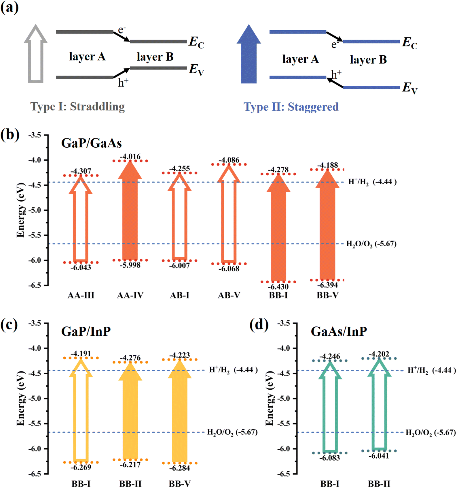 | ||
| Fig. 4 (a) The schematic illustration of vdW heterostructure with type-I and type-II band alignment. (b)–(d) The band edge alignments of vdW heterostructures with the possibility of photocatalysis. The hollow bars and filled bars represent type-I and type-II band alignment types, respectively. | ||
For a photocatalysis process, the absorption of the visible light is also important. After screening based on band parameters, we calculated the light absorption properties of the 5 selected configurations. As shown in Fig. 5, all of these heterostructures exhibit good light absorption in the ultraviolet and visible-light regions. For GaP/GaAs stacking-BB-V and GaP/InP stacking-BB-V, there is also absorption in the infrared region, suggesting that these special configurations could help extend the wavelength range of light absorption. Notably, the absorption coefficients of the heterostructures are greater than those of their individual monolayers, indicating that the formation of the heterostructure is beneficial for light absorption. Among all these 5 configurations, stacking BB-II GaP/InP has the largest light absorption, suggesting that it is the most promising material for use in photocatalysis applications.
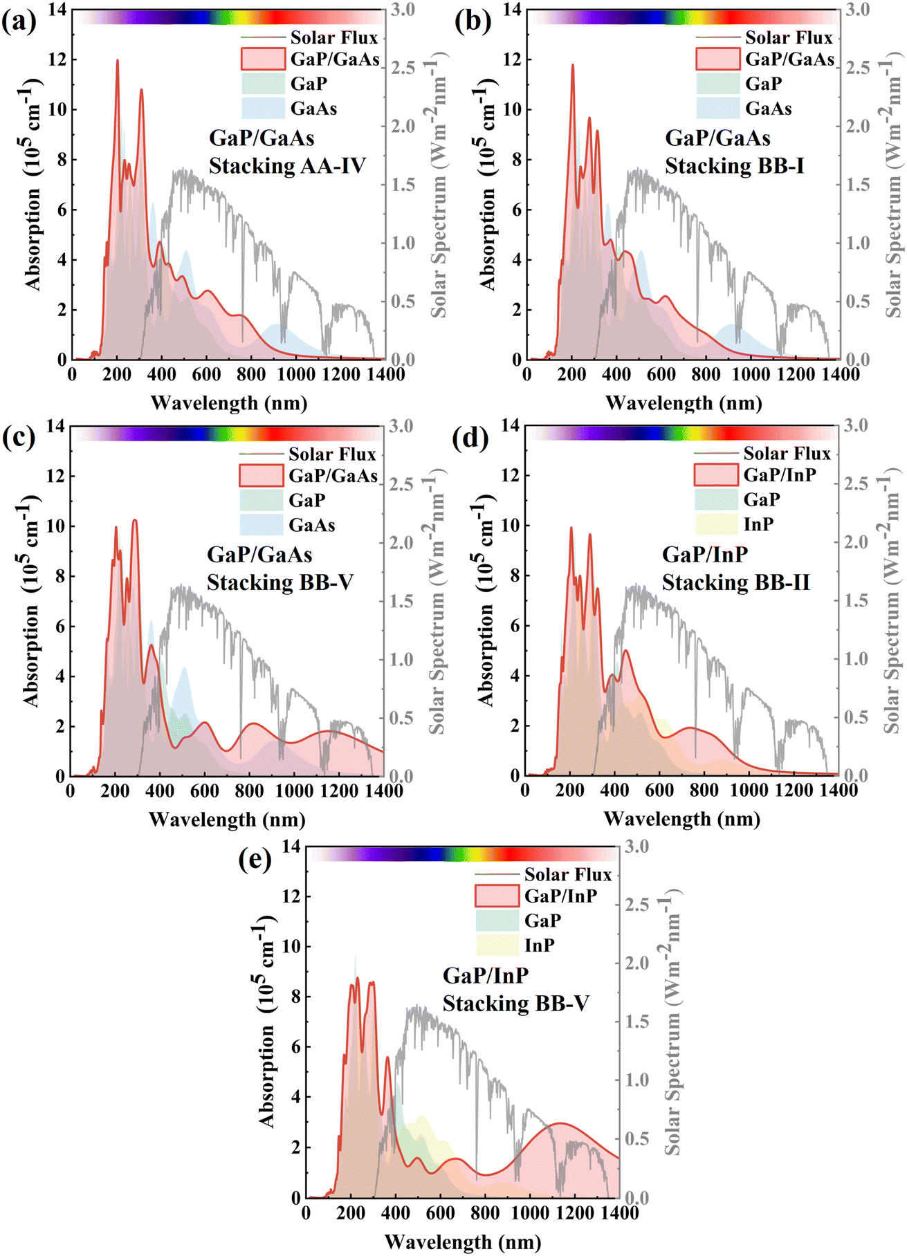 | ||
| Fig. 5 The absorption coefficients of (a) GaP/GaAs (stacking AA-IV), (b) GaP/GaAs (stacking BB-I), (c) GaP/GaAs (stacking BB-V), (d) GaP/InP (stacking BB-II), and (e) GaP/InP (stacking BB-V) heterostructures, respectively. The absorption of the corresponding pristine monolayers and the solar radiation spectrum are shown for reference. | ||
IV. Conclusion
In summary, we investigated the structural, electronic, and optical properties of the vdW heterostructures constructed by the 2D MX (M = Ga, In and X = P, As) monolayers using first-principles calculations to search for potential photocatalysts. There are six different combinations of heterostructure with 24 different configurations each. Out of 144 possible configurations, 130 are found to be energetically stable. Through electronic structure calculations, 34 configurations with bandgaps over 1.23 eV are selected. To successfully split the water into hydrogen and oxygen, 11 configurations could fulfill the requirements of the band edge alignment. Furthermore, there are 5 configurations with type-II band alignment and this is more beneficial for the photocatalysis application. Moreover, these 5 configurations are all found to have good light absorption, which ensures their potential for photocatalysis. Among them, stacking BB-II GaP/InP could be the most promising one, with its CBM being located at −4.276 eV and VBM being located at −6.217 eV. Overall, this research will provide insights into the discovery of new efficient photocatalysts and the application of the group III–V materials.Author contributions
Yingjie Chen: conceptualization, writing – original draft, writing – review & editing. Baonan Jia: visualization, conceptualization, writing – review & editing. Guoying Qin: investigation. Huiyan Zhao: formal analysis, software. Lihong Han: writing – review & editing. Pengfei Lu: writing – review & editing, supervision.Conflicts of interest
The authors declare that they have no known competing financial interests or personal relationships that could have appeared to influence the work reported in this paper.Acknowledgements
This work is supported by the National Key Research and Development Program of China (No. 2021YFA0718801), Foundation of Laboratory of Computational Physics (No. 6142A05QN22017), Project funded by China Postdoctoral Science Foundation (No. 2022M720516), and BUPT Excellent Ph.D. Students Foundation (No. CX2022309). We thank for the helpful discussion with Prof. Pengfei Guan and the computational support from the Beijing Computational Science Research Center (CSRC).References
- Y. Yang, J. Gu, J. L. Young, E. M. Miller, J. A. Turner, N. R. Neale and M. C. Beard, Science, 2015, 350, 1061–1065 CrossRef CAS PubMed.
- J. L. Young, M. A. Steiner, H. Doescher, R. M. France, J. A. Turner and T. G. Deutsch, Nat. Energy, 2017, 2, 17028 CrossRef CAS.
- L. A. King, T. R. Hellstern, J. Park, R. Sinclair and T. F. Jaramillo, ACS Appl. Mater. Interfaces, 2017, 9, 36792–36798 CrossRef CAS PubMed.
- D. Kang, J. L. Young, H. Lim, W. E. Klein, H. Chen, Y. Xi, B. Gai, T. G. Deutsch and J. Yoon, Nat. Energy, 2017, 2, 17043 CrossRef CAS.
- J. Gu, Y. Yan, J. L. Young, K. X. Steirer, N. R. Neale and J. A. Turner, Nat. Mater., 2016, 15, 456–460 CrossRef CAS PubMed.
- H. Lim, J. L. Young, J. F. Geisz, D. J. Friedman, T. G. Deutsch and J. Yoon, Nat. Commun., 2019, 10, 3388 CrossRef PubMed.
- S. Vanka, E. Arca, S. Cheng, K. Sun, G. A. Botton, G. Teeter and Z. Mi, Nano Lett., 2018, 18, 6530–6537 CrossRef CAS PubMed.
- J. Schneider, M. Matsuoka, M. Takeuchi, J. Zhang, Y. Horiuchi, M. Anpo and D. W. Bahnemann, Chem. Rev., 2014, 114, 9919–9986 CrossRef CAS PubMed.
- R. J. Britto, J. D. Benck, J. L. Young, C. Hahn, T. G. Deutsch and T. F. Jaramillo, J. Phys. Chem. Lett., 2016, 7, 2044–2049 CrossRef CAS PubMed.
- K. Sivula and R. van de Krol, Nat. Rev. Mater., 2016, 1, 15010 CrossRef CAS.
- A. K. Geim and I. V. Grigorieva, Nature, 2013, 499, 419–425 CrossRef CAS PubMed.
- Y. Liu, N. O. Weiss, X. Duan, H.-C. Cheng, Y. Huang and X. Duan, Nat. Rev. Mater., 2016, 1, 16042 CrossRef CAS.
- Z. Guo, N. Miao, J. Zhou, B. Sa and Z. Sun, J. Mater. Chem. C, 2017, 5, 978–984 RSC.
- G. Rehman, S. A. Khan, B. Amin, I. Ahmad, L.-Y. Gan and M. Maqbool, J. Mater. Chem. C, 2018, 6, 2830–2839 RSC.
- Q. Yang, S. Zhang, C. Tan, H. Ye, X. Ming, S. Ingebrandt and X. Chen, J. Mater. Chem. C, 2017, 5, 9412–9420 RSC.
- P. Hohenberg and W. Kohn, Phys. Rev., 1964, 136, B864–B871 CrossRef.
- J. P. Perdew, K. Burke and M. Ernzerhof, Phys. Rev. Lett., 1997, 78, 1396 CrossRef CAS.
- W. Kohn and L. J. Sham, Phys. Rev., 1965, 140, A1133–A1138 CrossRef.
- P. E. Blöchl, Phys. Rev. B: Condens. Matter Mater. Phys., 1994, 50, 17953 CrossRef PubMed.
- G. Kresse and J. Furthmüller, Phys. Rev. B: Condens. Matter Mater. Phys., 1996, 54, 11169–11186 CrossRef CAS PubMed.
- J. Heyd, G. E. Scuseria and M. Ernzerhof, J. Chem. Phys., 2003, 118, 8207–8215 CrossRef CAS.
- H. J. Monkhorst and J. D. Pack, Phys. Rev. B: Solid State, 1976, 13, 5188 CrossRef.
- S. Grimme, S. Ehrlich and L. Goerigk, J. Comput. Chem., 2011, 32, 1456–1465 CrossRef CAS PubMed.
- Y. Gao, D. Sun, X. Jiang and J. Zhao, J. Appl. Phys., 2019, 125, 215705 CrossRef.
- H. L. Zhuang, A. K. Singh and R. G. Hennig, Phys. Rev. B: Condens. Matter Mater. Phys., 2013, 87, 165415 CrossRef.
- H. Sahin, S. Cahangirov, M. Topsakal, E. Bekaroglu, E. Akturk, R. T. Senger and S. Ciraci, Phys. Rev. B: Condens. Matter Mater. Phys., 2009, 80, 155453 CrossRef.
- Y. Chen, B. Jia, X. Guan, L. Han, L. Wu, P. Guan and P. Lu, Appl. Surf. Sci., 2022, 586, 152799 CrossRef CAS.
- T. Bjorkman, A. Gulans, A. V. Krasheninnikov and R. M. Nieminen, Phys. Rev. Lett., 2012, 108, 235502 CrossRef CAS PubMed.
- K. Ren, Y. Liu, J. Yu and W. Tang, Chem. Phys., 2020, 528, 110539 CrossRef CAS.
- J. Heyd, J. E. Peralta, G. E. Scuseria and R. L. Martin, J. Chem. Phys., 2005, 123, 174101 CrossRef PubMed.
Footnote |
| † Electronic supplementary information (ESI) available. See DOI: https://doi.org/10.1039/d3ra01429k |
| This journal is © The Royal Society of Chemistry 2023 |